US5905407A - High efficiency power amplifier using combined linear and switching techniques with novel feedback system - Google Patents
High efficiency power amplifier using combined linear and switching techniques with novel feedback systemDownload PDFInfo
- Publication number
- US5905407A US5905407AUS08/902,802US90280297AUS5905407AUS 5905407 AUS5905407 AUS 5905407AUS 90280297 AUS90280297 AUS 90280297AUS 5905407 AUS5905407 AUS 5905407A
- Authority
- US
- United States
- Prior art keywords
- coupled
- amplifier
- signal
- output
- reference signal
- Prior art date
- Legal status (The legal status is an assumption and is not a legal conclusion. Google has not performed a legal analysis and makes no representation as to the accuracy of the status listed.)
- Expired - Lifetime
Links
- 238000000034methodMethods0.000titledescription6
- 238000012986modificationMethods0.000claimsdescription5
- 230000004048modificationEffects0.000claimsdescription5
- 238000010586diagramMethods0.000description20
- 239000003990capacitorSubstances0.000description17
- 230000001419dependent effectEffects0.000description6
- 230000000694effectsEffects0.000description2
- 238000001914filtrationMethods0.000description2
- 230000006872improvementEffects0.000description2
- 230000008569processEffects0.000description2
- 238000012546transferMethods0.000description2
- 230000003044adaptive effectEffects0.000description1
- 230000002411adverseEffects0.000description1
- 230000002238attenuated effectEffects0.000description1
- 230000008901benefitEffects0.000description1
- 230000008859changeEffects0.000description1
- 238000006243chemical reactionMethods0.000description1
- 230000000295complement effectEffects0.000description1
- 230000001143conditioned effectEffects0.000description1
- 230000014509gene expressionEffects0.000description1
- 238000012544monitoring processMethods0.000description1
- 230000004044responseEffects0.000description1
- 238000004088simulationMethods0.000description1
- 230000001360synchronised effectEffects0.000description1
- 238000012360testing methodMethods0.000description1
- 230000001052transient effectEffects0.000description1
- 230000007704transitionEffects0.000description1
Images


Classifications
- H—ELECTRICITY
- H03—ELECTRONIC CIRCUITRY
- H03F—AMPLIFIERS
- H03F1/00—Details of amplifiers with only discharge tubes, only semiconductor devices or only unspecified devices as amplifying elements
- H03F1/02—Modifications of amplifiers to raise the efficiency, e.g. gliding Class A stages, use of an auxiliary oscillation
- H03F1/0205—Modifications of amplifiers to raise the efficiency, e.g. gliding Class A stages, use of an auxiliary oscillation in transistor amplifiers
- H03F1/0211—Modifications of amplifiers to raise the efficiency, e.g. gliding Class A stages, use of an auxiliary oscillation in transistor amplifiers with control of the supply voltage or current
- H03F1/0216—Continuous control
- H03F1/0222—Continuous control by using a signal derived from the input signal
- H03F1/0227—Continuous control by using a signal derived from the input signal using supply converters
- H—ELECTRICITY
- H03—ELECTRONIC CIRCUITRY
- H03F—AMPLIFIERS
- H03F1/00—Details of amplifiers with only discharge tubes, only semiconductor devices or only unspecified devices as amplifying elements
- H03F1/02—Modifications of amplifiers to raise the efficiency, e.g. gliding Class A stages, use of an auxiliary oscillation
- H03F1/0205—Modifications of amplifiers to raise the efficiency, e.g. gliding Class A stages, use of an auxiliary oscillation in transistor amplifiers
- H03F1/0277—Selecting one or more amplifiers from a plurality of amplifiers
- H—ELECTRICITY
- H03—ELECTRONIC CIRCUITRY
- H03F—AMPLIFIERS
- H03F2200/00—Indexing scheme relating to amplifiers
- H03F2200/432—Two or more amplifiers of different type are coupled in parallel at the input or output, e.g. a class D and a linear amplifier, a class B and a class A amplifier
Definitions
- This inventionrelates in general to amplifiers, and more specifically to high efficiency power amplifiers as applied to radio frequency transmitters.
- a switching amplifieris known to produce switching noise.
- Prior art switching amplifiershave used passive filtering to reduce the switching noise. Such filtering limits the bandwidth of the amplifier, adversely affecting the slew rate and transient response time of the amplifier.
- An aspect of the present inventionis an amplifier apparatus.
- the amplifier apparatuscomprises an output node having an output voltage, and a switching amplifier having a first output coupled to the output node for delivering a switching amplifier output current to the output node.
- the amplifier apparatusfurther comprises a modulator coupled to the switching amplifier for controlling the switching amplifier, and a linear amplifier producing a linear amplifier output current through a second output coupled to the output node.
- the amplifier apparatusalso includes a feedback network coupled to the modulator for controlling the modulator, the feedback network also coupled to a reference signal which the amplifier apparatus tracks, the feedback network further coupled to a current sense signal proportional to the linear amplifier output current, and coupled to a switching amplifier signal internal to the switching amplifier, the switching amplifier signal not derived from the output voltage and not generated by sensing the switching amplifier output current.
- the radio transmittercomprises a power supply reference generator for generating a reference signal, and an amplifier apparatus coupled to the power supply reference generator for generating an output signal that tracks the reference signal.
- the radio transmitterfurther comprises a radio frequency (RF) power amplifier coupled to the amplifier apparatus for amplifying an RF signal, the RF power amplifier powered by the output signal of the amplifier apparatus and producing an amplified RF signal; and an RF source for generating the RF signal.
- the amplifier apparatuscomprises an output node having an output voltage, and a switching amplifier having a first output coupled to the output node for delivering a switching amplifier output current to the output node.
- the amplifier apparatusfurther comprises a modulator coupled to the switching amplifier for controlling the switching amplifier, and a linear amplifier producing a linear amplifier output current through a second output coupled to the output node.
- the amplifier apparatusalso includes a feedback network coupled to the modulator for controlling the modulator, the feedback network also coupled to the reference signal, which the amplifier apparatus tracks, the feedback network further coupled to a current sense signal proportional to the linear amplifier output current, and coupled to a switching amplifier signal internal to the switching amplifier, the switching amplifier signal not derived from the output voltage and not generated by sensing the switching amplifier output current.
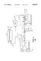
- FIG. 1is a generic electrical block diagram of a power amplifier in accordance with the present invention.
- FIG. 2is an electrical block diagram detailing a feedback network, a modulator, and a switching amplifier of a first embodiment of the power amplifier in accordance with the present invention.
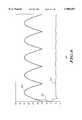
- FIG. 3is a performance diagram of the first embodiment in accordance with the present invention.
- FIG. 4is an electrical block diagram of a second embodiment of the power amplifier in accordance with the present invention.
- FIG. 5is an electrical block diagram detailing a feedback network and a switching amplifier of the second embodiment of the power amplifier in is accordance with the present invention.
- FIG. 6is a performance diagram of the second embodiment in accordance with the present invention.
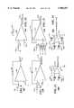
- FIG. 7is an electrical block diagram of an auto tuning circuit in accordance with the present invention.
- FIG. 8is an electrical block diagram of a radio transmitter in accordance with the present invention.
- FIGS. 9-14are exemplary electrical block diagrams detailing portions of the feedback network in accordance with the present invention.
- FIG. 15is a performance diagram of the first embodiment when tuned with the auto tuning circuit of FIG. 7 in accordance with the present invention.
- FIG. 1is a generic electrical block diagram of a power amplifier 100 in accordance with the present invention.
- the amplifier 100includes a linear amplifier 102 comprising a conventional power operational amplifier 116 coupled to a reference signal V ref at a positive input 122.
- the power operational amplifier 116is the PA04A amplifier manufactured by Apex-Microtech of Arlington, Ariz. It will be appreciated that other similar amplifiers can be used as well for the amplifier 116.
- the output 118 of the operational amplifier 116is coupled to the negative input 120, such that the voltage at the output 118 of the operational amplifier 116 tracks the reference signal V ref .
- the reference signal V refis the desired output voltage of the amplifier 100.
- the output 118is coupled through a resistor 108 to an output node 114.
- the resistance of the resistor 108is preferably small, relative to the impedance of a load 111 coupled between the output node 114 and a common node 113, e.g., 1 percent of the load impedance.
- Inputs of a conventional differential amplifier 110are coupled across the resistor 108 for generating a current sense voltage I sen proportional to the output current I lin of the linear amplifier 102 at a current sense output 112.
- the output 132 of a conventional switching amplifier 104is coupled in parallel with the linear amplifier 102 at the output node 114.
- the switching amplifier 104comprises at least one switch 126 for switching an input voltage V in across at least one filter comprising an inductor 124 and a capacitor 128.
- the duty cycle of the switch(es) 126is controlled by a signal from a modulator 136 having a modulator output 134 and coupled to a feedback network 106 for receiving a control signal therefrom.
- the switch modulationpreferably is pulse width modulation (PWM). This has the advantage of having a fixed frequency of operation and of being synchronized externally.
- the sensing of the output current I SW of the switching amplifier 104preferably is avoided due to noise and signal to noise ratio (SNR) considerations.
- SNRsignal to noise ratio
- the linear amplifier 102is connected to the load 111 directly (except for the small resistor 108), the linear amplifier 102 substantially determines the output voltage V out at the output node 114. This greatly reduces the switching ripple present in the output, thereby advantageously allowing a more efficient, lower switching frequency to be utilized for the switching amplifier 104.
- the output voltage V outis, however, not suitable for control of the switching amplifier 104. It is therefore preferable to construct a feedback scheme which does not require output feedback.
- Inputs to the feedback network 106include the reference signal V ref , the current sense voltage I sen , and at least one signal V int internal to the switching amplifier 104, the at least one signal V int not derived from the output voltage across the load 111 and not generated by sensing the output current of the switching amplifier 104.
- the feedback network 106, the modulator 136 and the switching amplifier 104cooperate to regulate the output current I SW of the switching amplifier such that the average value of the output current I lin of the linear amplifier 102 is driven to zero, thereby maximizing the efficiency of the amplifier 100.
- FIG. 2is an electrical block diagram detailing the feedback network 106 and the modulator 136, along with a conventional switching amplifier 202 of a first embodiment 200 of the power amplifier 100 in accordance with the present invention.
- the first embodiment 200includes a switching amplifier 202 for efficiently delivering a switching amplifier output current I SW to the output node 114.
- the switching amplifier 202preferably comprises two switches 252, which operate in a complementary fashion, one switch 252 being closed, while the other switch 252 is open, and vice versa, with a duty cycle controlled by the modulator 136, which preferably is a conventional pulse width modulator (PWM) circuit.
- PWMpulse width modulator
- the switches 252are constructed from conventional switching transistors.
- the switching amplifier 202includes a single-stage filter comprising an inductor 254 coupled between a switching node 204 (which serves as the input node of the single-stage filter) and the output node 114.
- the filterfurther comprises a capacitor 256 coupled between the output node 114 and a common node 113.
- the switching amplifieris coupled to the output 224 of the modulator 136.
- the modulator 136preferably comprises a conventional comparator 218 coupled to a conventional latch 220.
- One input 222 of the comparator 218is coupled to a ramp signal generated by a conventional ramp generator (not shown).
- the other input of the comparator 218is coupled to the output 214 of a subtraction integrator 208 of the feedback network 106.
- the feedback network 106is preferably coupled to the switching node 204 of the switching amplifier for monitoring the voltage V SW present on the switching node 204.
- the voltage V SWpreferably is coupled to the negative input 210 of the subtraction integrator 208 whose output is the output signal Sig of the feedback network 106.
- the positive input 212 of the subtraction integrator 208is coupled to the output of a first summer 232.
- a first input of the first summer 232is coupled to an intermediate signal V ref' to generated from the reference signal V ref and time derivatives of V ref in a manner that will be described below.
- a second input of the first summer 232preferably is coupled to the output 230 of a proportional plus integral (P.I.) circuit 228. The input of the P.I.
- the P.I. circuit 228is coupled to the current sense output 112 of the differential amplifier 110.
- the P.I. circuit 228generates a signal (aI sen +b ⁇ I sen ) that is proportional to both I sen and the integral of I sen .
- the P.I. circuitcan be omitted and the second input of the summer 232 can be connected directly to the current sense output 112.
- the intermediate signal V ref'is generated at the output 234 of a second summer 236.
- the inputs of the second summer 236are coupled to the reference signal V ref and to first and second outputs 240, 238 of first and second differentiators 242 and 250, respectively.
- the input 244 of the first differentiator 242is coupled to the reference signal V ref .
- the gain of the first differentiator 242is such that it generates an output signal equal to K 0 ⁇ dV ref /dt.
- the input 248 of the second differentiator 250is coupled to the output 240 of the first differentiator 242.
- the gain of the second differentiator 250is such that it generates an output signal equal to K 1 ⁇ d 2 V ref /dt 2 .
- K 0 and K 1are defined below.
- Detailed examples of circuits for realizing the building blocks, e.g., the differentiators 242, 250 and the summers 232, 236, of this and other embodiments of the feedback network 106are disclosed
- the PWM circuitis a sampled data system with variable delay between 0 and Ts, the period of the ramp signal at the input 222, depending upon the duty ratio required.
- the average delayis Ts/2. This delay is small compared to the delay in the output filter of the switching amplifier 202. This delay can also be compensated using the time derivatives of the reference signal Vref.
- the expressions for the coefficients K 0 and K 1can be computed a priori when the nominal value of the load impedance is known (R). Alternatively, the coefficients K 0 and K 1 can be computed by a tuning technique.
- the nominal values of K 0 and K 1are as follows. ##EQU2##
- the feedback signal Sigis generated in terms of the modified reference signal V ref' , the switch voltage V SW , and the current sense voltage I sen .
- the linear amplifier currentpreferably is conditioned with a P.I. block. ##EQU3##
- the PI blockcan be omitted.
- the gain of the feedback signal Sigpreferably is determined by the well known "equal slope criterion", which is optimal for PWM conversion.
- the average value of the linear amplifier currentbecomes equal to the resistive voltage drop in the inductor (L).
- the two-pole switching amplifier systemwas simulated, built and tested. The results are depicted in FIG. 3, a performance diagram 300 of the first embodiment in accordance with the present invention.
- the graph 302depicts the reference signal V ref , which is the desired output voltage.
- the graph 304is the output voltage V out . Note that the output voltage V out tracks the reference signal V ref very closely except for a brief instant at start-up.
- the graph 306depicts the output current I lin of the linear amplifier 102. Note that the average value of I lin advantageously is driven near zero.
- a limitation encountered with the first embodiment of the power amplifier 100was that the switching noise was not attenuated as much as desired.
- the ability of the linear amplifier 102 to suppress noiseis reduced at higher frequencies, while the switching noise can be reduced for a given switching amplifier only by going to a higher frequency.
- the solutionis to use a higher order filter, as disclosed herein below for the second embodiment 400 of the power amplifier 100 in accordance with the present invention.
- FIG. 4is an electrical block diagram of the second embodiment 400.
- the second embodiment 400is similar to the first embodiment 200, the essential differences being a switching amplifier 402 having a two-stage filter, and a minor change in the feedback network 106, which will be described further below.
- the switching amplifier 402comprises a first filter stage L1, C1 and a second filter stage L2, C2.
- the first inductor L1is coupled between the switching node 204 (which serves as the first-stage input node) and an intermediate node 406 (which serves as the second-stage input node) having a voltage V C1 .
- the first capacitor C1is coupled between the intermediate node 406 and the common node 113.
- the second inductor L2is coupled between the intermediate node 406 and the output node 114.
- the second capacitor C2is coupled between the output node 114 and the common node 113.
- FIG. 5is an electrical block diagram 500 detailing the feedback network 106 and the switching amplifier 402 of the second embodiment of the power amplifier 100 in accordance with the present invention.
- the feedback network 106 of FIG. 5is similar to the feedback network 106 depicted in FIG. 2, the essential difference being the addition of a summer 510 and a subtraction P.I. circuit 506.
- the output 512 of the summer 510carries the output signal Sig of the feedback network 106 and is coupled to the PWM circuit for controlling the PWM duty cycle.
- One input of the summer 510is coupled to the output 214 of the subtraction integrator 208.
- Another input of the summer 510is coupled to the output 508 of the subtraction P.I. circuit 506.
- circuit 506is coupled to the output 234 of the summer 236 for receiving the intermediate signal V ref' .
- the negative input of the subtraction P.I. circuit 506is coupled to the intermediate node 406 of the switching amplifier 402 for receiving the voltage V C1 from the switching amplifier 402.
- FIG. 6is a performance diagram 600 of the second embodiment in accordance with the present invention.
- the graphs 602, 604, and 606depict the reference signal V ref , the output voltage V out , and the linear amplifier current I lin , respectively.
- the switching noisehas been reduced due to the fourth order filter.
- the filterhas high rejection of the switching noise while allowing relatively high frequencies to pass through.
- the linear amplifier 102is active only at times when the reference signal V ref has a sharp transition. This is in contrast to the two pole filter, where the linear amplifier 102 has to cancel a significant current ripple as shown in FIG. 3.
- FIG. 7is an electrical block diagram of an auto tuning circuit 700 in accordance with the present invention.
- the auto tuning circuit 700replaces the first and second differentiators 242, 250 with two differentiators 738, 740, four multipliers 704, 716, 722, 732, and two integrators 710, 728.
- the multipliers 704, 716, 722, 732are similar to the AD633 multiplier manufactured by Analog Devices, Inc. of Norwood, Mass. It will be appreciated that other similar multipliers can be used as well for the multipliers 704, 716, 722, 732.
- the inputs 702, 706 of the first multiplier 704are coupled, respectively, to the current sense output 112 for receiving the current sense voltage I sen , and to the output 744 of a first differentiator 738 having an input coupled to the reference signal V ref .
- the first differentiator 738generates a signal representing the derivative of the reference signal dV ref /dt.
- the output 708 of the first multiplier 704is coupled to the first integrator 710, whose output is coupled to a first input 712 of the second multiplier 716.
- the first integrator 710generates a value representing the coefficient K 1 .
- a second input 714 of the second multiplier 716is coupled to the output 746 of the second differentiator 740.
- the input of the second differentiatoris coupled to the output 744 of the first differentiator 738.
- the output of the second differentiator 740represents the second derivative of the reference signal d 2 V ref /dt 2 .
- the output of the second multiplier 716thus represents the signal K 1 ⁇ d 2 V ref /dt 2 ⁇ , which is coupled to a first input 718 of the second summer 236 for generating V ref' at the output 234.
- Inputs 720, 724 of the third multiplier 722are coupled, respectively, to I sen and V ref .
- the output 726 of the third multiplier 722is coupled to the input of the second integrator 728.
- the second integrator 728generates a signal representing the coefficient K 0 .
- This signalis coupled to a first input 730 of the fourth multiplier 732.
- a second input 734 of the fourth multiplier 732is coupled to the output 744 of the first differentiator 738, representing the derivative of the reference signal dV ref /dt.
- the output of the fourth multiplier 732thus represents the signal K 0 ⁇ dV ref /dt ⁇ , which is coupled to a second input 736 of the second summer 236.
- a third input 246 of the second summeris coupled to the reference signal V ref .
- the auto tuning circuit 700operates to tune the values of the coefficients K 0 and K 1 .
- the linear amplifier current I lin(represented by the sense voltage I sen ) is effectively the error in the current output of the switching amplifier. Thus it can be used as an error signal for tuning the coefficients K 0 and K 1 .
- An error in K 0results in an error of K 0 ⁇ V ref in the switching amplifier current.
- an error in K 1results in an error of K 1 ⁇ (dVref/dt).
- the values for K 0 and K 1are constant. This implies that the integrand has no dc value.
- the integrand in this caseis V ref ⁇ I sen and (dV ref /dt) ⁇ I sen for K 0 and K 1 , respectively. This condition is satisfied when I sen is mathematically uncorrelated to V ref and its time derivative.
- the feedback to the switching amplifier 104is optimized. Performance of the auto tuning circuit 700 is described further below.
- FIG. 8is an electrical block diagram of a radio transmitter 800 in accordance with the present invention.
- the radio transmitter 800comprises the power amplifier 100 as disclosed herein above, and a power supply reference generator 802 coupled to the linear amplifier 102 and coupled to the feedback network 106 for providing the reference signal V ref thereto.
- the radio transmitter 800further comprises a radio frequency (RF) power amplifier 806 coupled to the output node 114 for receiving the output voltage V out as a supply voltage for the RF power amplifier 806.
- the radio transmitter 800comprises an RF source 804 coupled to the RF power amplifier 806 for generating an RF signal which is amplified by the RF power amplifier 806, and an RF load, such as an antenna, coupled to the RF power amplifier 806.
- RFradio frequency
- the power supply reference generator 802is also coupled to the RF source for synchronizing the power supply reference generator 802 with an amplitude modulation of the RF source.
- the power amplifier 100can supply the RF power amplifier 806 with just enough supply voltage to meet the needs of the RF power amplifier 806 at each instant, thereby greatly improving the efficiency of the RF power amplifier 806.
- FIGS. 9-14are exemplary electrical block diagrams detailing portions of the feedback network 106 in accordance with the present invention.
- FIG. 9is a differentiator 900.
- the differentiator 900comprises a capacitor 902 coupled to the negative input 908 of a conventional operational amplifier, such as the MC34074A operational amplifier manufactured by Motorola, Inc. of Schaumburg, Ill.
- a resistor 906is coupled from the output 912 to the negative input 908.
- the positive input 910is coupled to a common node, such as circuit ground.
- the output 912produces a voltage of -kdV/dt, the value of k dependent upon the relative values of the resistor 906 and the capacitor 902.
- the differentiator 900is an exemplary circuit for the differentiators 242, 250, 738, 740. It will be appreciated that, alternatively, other similar circuits for differentiators can be used as well for the differentiators 242, 250, 738, 740.
- FIG. 10is a P.I. circuit 1000.
- the P.I. circuit 1000comprises a first resistor 1002 coupled between a common node and the negative input 1004 of a conventional operational amplifier 1008.
- a capacitor 1010 and a second resistor 1014are series coupled between the negative input 1004 and the output 1012 of the amplifier 1008.
- VWhen a voltage V is applied to the positive input 1006, the output produces a voltage of aV+b ⁇ Integral(V) ⁇ , the values of the constants a and b dependent upon the relative values of the resistor 1002 and the capacitor 1010.
- the P.I. circuit 1000is an exemplary circuit for the P.I. circuits 228, 506. It will be appreciated that, alternatively, other similar P.I. circuits can be used as well for the P.I. circuits 228, 506.
- FIG. 11is an integrator 1100.
- the integrator 1100comprises a resistor 1102 coupled to the negative input 1104 of a conventional operational amplifier 1108.
- a capacitor 1110is coupled between the negative input 1104 and the output 1112.
- the positive input 1106is coupled to a common node.
- VWhen a voltage V is applied to the uncoupled end of the resistor 1102, the output produces a voltage equal to -k ⁇ Integral(V) ⁇ , the value of k dependent upon the relative values of the capacitor 1110 and the resistor 1102.
- the integrator 1100is an exemplary circuit for the integrators 710, 728. It will be appreciated that, alternatively, other similar integrator circuits can be used as well for the integrators 710, 728.
- FIG. 12is a summer 1200.
- the summer 1200comprises a first resistor 1202 coupled between a common node and the negative input 1210 of a conventional operational amplifier 1214.
- a second resistor 1218is coupled between the output 1216 and the negative input 1210.
- Third, fourth, and fifth resistors 1204, 1206, and 1208are coupled to the positive input of the amplifier 1214.
- the output 1216produces a voltage equal to k(V1+V2+V3), k dependent upon the relative values of the resistors 1202-1208 and 1218.
- the summer 1200is an exemplary circuit for the summers 232, 236, 510. It will be appreciated that, alternatively, other similar summers can be used as well for the summers 232, 236, 510.
- FIG. 13is a subtraction integrator 1300.
- the subtraction integrator 1300comprises a first resistor 1302 coupled to the negative input 1304 of a conventional operational amplifier 1310.
- a first capacitor 1312is coupled between the output 1316 and the negative input 1304.
- a second resistor 1306is coupled to the positive input 1308.
- a second capacitor 1314is coupled between the positive input 1308 and a common node.
- FIG. 14is a subtraction P.I. circuit 1400.
- the subtraction P.I. circuit 1400comprises a first resistor 1402 coupled to the negative input 1404 of a conventional operational amplifier 1420.
- a first capacitor 1410 and a second resistor 1412are series coupled between the output 1418 and the negative input 1404.
- the subtraction P.I. circuit 1400further comprises a third resistor 1406 coupled to the positive input 1408.
- a second capacitor 1414 and a fourth resistor 1416are series coupled between the positive input 1408 and a common node.
- the subtraction P.I. circuit 1400is an exemplary circuit for the subtraction PI. circuit 506. It will be appreciated that, alternatively, other similar subtraction P.I. circuits can be used as well for the subtraction P.I. circuit 506.
- FIG. 15is a performance diagram of the first embodiment when tuned with the auto tuning circuit of FIG. 7 in accordance with the present invention.
- the graph 1502depicts both the reference signal V ref and the output voltage V out .
- the graph 1504represents the linear amplifier current I lin . Note that the linear amplifier current I lin has been minimized and is equal to the ripple current only. The tuning process can be made faster or slower depending on the amount of noise in the linear amplifier current. The simultaneous tuning of the terms proportional to the reference signal V ref and its derivative is possible since the two terms are orthogonal in longer time frames. In the simulation depicted, the initial values were chosen to be zero. Testing was also done with various initial values and the results are independent of the initial conditions.
Landscapes
- Engineering & Computer Science (AREA)
- Power Engineering (AREA)
- Amplifiers (AREA)
Abstract
Description
This invention relates in general to amplifiers, and more specifically to high efficiency power amplifiers as applied to radio frequency transmitters.
To obtain high efficiency in a baseband power amplifier it is necessary to use switching techniques. A switching amplifier is known to produce switching noise. Prior art switching amplifiers have used passive filtering to reduce the switching noise. Such filtering limits the bandwidth of the amplifier, adversely affecting the slew rate and transient response time of the amplifier.
One method of reducing the switching noise without limiting the bandwidth more than an acceptable amount has been to increase the switching frequency. An undesirable side effect of increased switching frequency, however, is increased power consumption.
Thus, what is needed is an apparatus for providing a high bandwidth, low noise baseband amplifier which operates at a lower switching frequency than possible in prior art switching amplifiers.
An aspect of the present invention is an amplifier apparatus. The amplifier apparatus comprises an output node having an output voltage, and a switching amplifier having a first output coupled to the output node for delivering a switching amplifier output current to the output node. The amplifier apparatus further comprises a modulator coupled to the switching amplifier for controlling the switching amplifier, and a linear amplifier producing a linear amplifier output current through a second output coupled to the output node. The amplifier apparatus also includes a feedback network coupled to the modulator for controlling the modulator, the feedback network also coupled to a reference signal which the amplifier apparatus tracks, the feedback network further coupled to a current sense signal proportional to the linear amplifier output current, and coupled to a switching amplifier signal internal to the switching amplifier, the switching amplifier signal not derived from the output voltage and not generated by sensing the switching amplifier output current.
Another aspect of the present invention is a radio transmitter. The radio transmitter comprises a power supply reference generator for generating a reference signal, and an amplifier apparatus coupled to the power supply reference generator for generating an output signal that tracks the reference signal. The radio transmitter further comprises a radio frequency (RF) power amplifier coupled to the amplifier apparatus for amplifying an RF signal, the RF power amplifier powered by the output signal of the amplifier apparatus and producing an amplified RF signal; and an RF source for generating the RF signal. The amplifier apparatus comprises an output node having an output voltage, and a switching amplifier having a first output coupled to the output node for delivering a switching amplifier output current to the output node. The amplifier apparatus further comprises a modulator coupled to the switching amplifier for controlling the switching amplifier, and a linear amplifier producing a linear amplifier output current through a second output coupled to the output node. The amplifier apparatus also includes a feedback network coupled to the modulator for controlling the modulator, the feedback network also coupled to the reference signal, which the amplifier apparatus tracks, the feedback network further coupled to a current sense signal proportional to the linear amplifier output current, and coupled to a switching amplifier signal internal to the switching amplifier, the switching amplifier signal not derived from the output voltage and not generated by sensing the switching amplifier output current.
FIG. 1 is a generic electrical block diagram of a power amplifier in accordance with the present invention.
FIG. 2 is an electrical block diagram detailing a feedback network, a modulator, and a switching amplifier of a first embodiment of the power amplifier in accordance with the present invention.
FIG. 3 is a performance diagram of the first embodiment in accordance with the present invention.
FIG. 4 is an electrical block diagram of a second embodiment of the power amplifier in accordance with the present invention.
FIG. 5 is an electrical block diagram detailing a feedback network and a switching amplifier of the second embodiment of the power amplifier in is accordance with the present invention.
FIG. 6 is a performance diagram of the second embodiment in accordance with the present invention.
FIG. 7 is an electrical block diagram of an auto tuning circuit in accordance with the present invention. FIG. 8 is an electrical block diagram of a radio transmitter in accordance with the present invention.
FIGS. 9-14 are exemplary electrical block diagrams detailing portions of the feedback network in accordance with the present invention.
FIG. 15 is a performance diagram of the first embodiment when tuned with the auto tuning circuit of FIG. 7 in accordance with the present invention.
FIG. 1 is a generic electrical block diagram of apower amplifier 100 in accordance with the present invention. Theamplifier 100 includes alinear amplifier 102 comprising a conventional poweroperational amplifier 116 coupled to a reference signal Vref at apositive input 122. Preferably, the poweroperational amplifier 116 is the PA04A amplifier manufactured by Apex-Microtech of Tucson, Ariz. It will be appreciated that other similar amplifiers can be used as well for theamplifier 116. Theoutput 118 of theoperational amplifier 116 is coupled to thenegative input 120, such that the voltage at theoutput 118 of theoperational amplifier 116 tracks the reference signal Vref. The reference signal Vref is the desired output voltage of theamplifier 100. Theoutput 118 is coupled through aresistor 108 to anoutput node 114. The resistance of theresistor 108 is preferably small, relative to the impedance of aload 111 coupled between theoutput node 114 and acommon node 113, e.g., 1 percent of the load impedance. Inputs of a conventionaldifferential amplifier 110 are coupled across theresistor 108 for generating a current sense voltage Isen proportional to the output current Ilin of thelinear amplifier 102 at acurrent sense output 112.
Theoutput 132 of aconventional switching amplifier 104 is coupled in parallel with thelinear amplifier 102 at theoutput node 114. Theswitching amplifier 104 comprises at least oneswitch 126 for switching an input voltage Vin across at least one filter comprising aninductor 124 and acapacitor 128. The duty cycle of the switch(es) 126 is controlled by a signal from amodulator 136 having amodulator output 134 and coupled to afeedback network 106 for receiving a control signal therefrom. The switch modulation preferably is pulse width modulation (PWM). This has the advantage of having a fixed frequency of operation and of being synchronized externally. The sensing of the output current ISW of theswitching amplifier 104 preferably is avoided due to noise and signal to noise ratio (SNR) considerations. Because thelinear amplifier 102 is connected to theload 111 directly (except for the small resistor 108), thelinear amplifier 102 substantially determines the output voltage Vout at theoutput node 114. This greatly reduces the switching ripple present in the output, thereby advantageously allowing a more efficient, lower switching frequency to be utilized for theswitching amplifier 104. The output voltage Vout is, however, not suitable for control of theswitching amplifier 104. It is therefore preferable to construct a feedback scheme which does not require output feedback.
Inputs to thefeedback network 106 include the reference signal Vref, the current sense voltage Isen, and at least one signal Vint internal to theswitching amplifier 104, the at least one signal Vint not derived from the output voltage across theload 111 and not generated by sensing the output current of theswitching amplifier 104. Thefeedback network 106, themodulator 136 and theswitching amplifier 104 cooperate to regulate the output current ISW of the switching amplifier such that the average value of the output current Ilin of thelinear amplifier 102 is driven to zero, thereby maximizing the efficiency of theamplifier 100.
FIG. 2 is an electrical block diagram detailing thefeedback network 106 and themodulator 136, along with aconventional switching amplifier 202 of a first embodiment 200 of thepower amplifier 100 in accordance with the present invention. The first embodiment 200 includes aswitching amplifier 202 for efficiently delivering a switching amplifier output current ISW to theoutput node 114. Theswitching amplifier 202 preferably comprises twoswitches 252, which operate in a complementary fashion, oneswitch 252 being closed, while theother switch 252 is open, and vice versa, with a duty cycle controlled by themodulator 136, which preferably is a conventional pulse width modulator (PWM) circuit. Preferably, theswitches 252 are constructed from conventional switching transistors. Theswitching amplifier 202 includes a single-stage filter comprising aninductor 254 coupled between a switching node 204 (which serves as the input node of the single-stage filter) and theoutput node 114. The filter further comprises acapacitor 256 coupled between theoutput node 114 and acommon node 113.
The switching amplifier is coupled to theoutput 224 of themodulator 136. Themodulator 136 preferably comprises aconventional comparator 218 coupled to aconventional latch 220. Oneinput 222 of thecomparator 218 is coupled to a ramp signal generated by a conventional ramp generator (not shown). The other input of thecomparator 218 is coupled to theoutput 214 of asubtraction integrator 208 of thefeedback network 106.
Thefeedback network 106 is preferably coupled to theswitching node 204 of the switching amplifier for monitoring the voltage VSW present on theswitching node 204. The voltage VSW preferably is coupled to thenegative input 210 of thesubtraction integrator 208 whose output is the output signal Sig of thefeedback network 106. Thepositive input 212 of thesubtraction integrator 208 is coupled to the output of afirst summer 232. A first input of thefirst summer 232 is coupled to an intermediate signal Vref' to generated from the reference signal Vref and time derivatives of Vref in a manner that will be described below. A second input of thefirst summer 232 preferably is coupled to theoutput 230 of a proportional plus integral (P.I.)circuit 228. The input of the P.I. circuit is coupled to thecurrent sense output 112 of thedifferential amplifier 110. The P.I.circuit 228 generates a signal (aIsen +b∫ Isen) that is proportional to both Isen and the integral of Isen. Alternatively, the P.I. circuit can be omitted and the second input of thesummer 232 can be connected directly to thecurrent sense output 112.
The intermediate signal Vref' is generated at theoutput 234 of asecond summer 236. The inputs of thesecond summer 236 are coupled to the reference signal Vref and to first andsecond outputs second differentiators input 244 of thefirst differentiator 242 is coupled to the reference signal Vref. The gain of thefirst differentiator 242 is such that it generates an output signal equal to K0 ×dVref /dt. Theinput 248 of thesecond differentiator 250 is coupled to theoutput 240 of thefirst differentiator 242. The gain of thesecond differentiator 250 is such that it generates an output signal equal to K1 ×d2 Vref /dt2. K0 and K1 are defined below. Detailed examples of circuits for realizing the building blocks, e.g., thedifferentiators summers feedback network 106 are disclosed further below.
The use of the time derivatives of the reference signal Vref is a departure from the prior art, and a considerable improvement is obtained. When the load impedance (R) is approximately known, the transfer function of the passive L-C-R filter is known. In effect, the inverse of this transfer function is constructed using the derivatives of the reference signal Vref. ##EQU1##
The PWM circuit is a sampled data system with variable delay between 0 and Ts, the period of the ramp signal at theinput 222, depending upon the duty ratio required. The average delay is Ts/2. This delay is small compared to the delay in the output filter of the switchingamplifier 202. This delay can also be compensated using the time derivatives of the reference signal Vref. The expressions for the coefficients K0 and K1 can be computed a priori when the nominal value of the load impedance is known (R). Alternatively, the coefficients K0 and K1 can be computed by a tuning technique. The nominal values of K0 and K1 are as follows. ##EQU2##
Note that the terms with Ts compensate for the delay of the PWM circuit, while the other terms compensate for the delay of the R-L-C filter. The feedback signal Sig is generated in terms of the modified reference signal Vref', the switch voltage VSW, and the current sense voltage Isen. The linear amplifier current preferably is conditioned with a P.I. block. ##EQU3##
Alternatively, the PI block can be omitted.
The gain of the feedback signal Sig preferably is determined by the well known "equal slope criterion", which is optimal for PWM conversion. When the P.I. block is omitted, the average value of the linear amplifier current becomes equal to the resistive voltage drop in the inductor (L).
The two-pole switching amplifier system was simulated, built and tested. The results are depicted in FIG. 3, a performance diagram 300 of the first embodiment in accordance with the present invention. Thegraph 302 depicts the reference signal Vref, which is the desired output voltage. Thegraph 304 is the output voltage Vout. Note that the output voltage Vout tracks the reference signal Vref very closely except for a brief instant at start-up.
Thegraph 306 depicts the output current Ilin of thelinear amplifier 102. Note that the average value of Ilin advantageously is driven near zero. A limitation encountered with the first embodiment of thepower amplifier 100 was that the switching noise was not attenuated as much as desired. The ability of thelinear amplifier 102 to suppress noise is reduced at higher frequencies, while the switching noise can be reduced for a given switching amplifier only by going to a higher frequency. The solution is to use a higher order filter, as disclosed herein below for thesecond embodiment 400 of thepower amplifier 100 in accordance with the present invention.
FIG. 4 is an electrical block diagram of thesecond embodiment 400. Thesecond embodiment 400 is similar to the first embodiment 200, the essential differences being a switchingamplifier 402 having a two-stage filter, and a minor change in thefeedback network 106, which will be described further below. The switchingamplifier 402 comprises a first filter stage L1, C1 and a second filter stage L2, C2. The first inductor L1 is coupled between the switching node 204 (which serves as the first-stage input node) and an intermediate node 406 (which serves as the second-stage input node) having a voltage VC1. The first capacitor C1 is coupled between theintermediate node 406 and thecommon node 113. The second inductor L2 is coupled between theintermediate node 406 and theoutput node 114. The second capacitor C2 is coupled between theoutput node 114 and thecommon node 113.
FIG. 5 is an electrical block diagram 500 detailing thefeedback network 106 and the switchingamplifier 402 of the second embodiment of thepower amplifier 100 in accordance with the present invention. Thefeedback network 106 of FIG. 5 is similar to thefeedback network 106 depicted in FIG. 2, the essential difference being the addition of asummer 510 and a subtraction P.I.circuit 506. Theoutput 512 of thesummer 510 carries the output signal Sig of thefeedback network 106 and is coupled to the PWM circuit for controlling the PWM duty cycle. One input of thesummer 510 is coupled to theoutput 214 of thesubtraction integrator 208. Another input of thesummer 510 is coupled to theoutput 508 of the subtraction P.I.circuit 506. The positive input of the subtraction P.I.circuit 506 is coupled to theoutput 234 of thesummer 236 for receiving the intermediate signal Vref'. The negative input of the subtraction P.I.circuit 506 is coupled to theintermediate node 406 of the switchingamplifier 402 for receiving the voltage VC1 from the switchingamplifier 402.
FIG. 6 is a performance diagram 600 of the second embodiment in accordance with the present invention. Thegraphs linear amplifier 102 is active only at times when the reference signal Vref has a sharp transition. This is in contrast to the two pole filter, where thelinear amplifier 102 has to cancel a significant current ripple as shown in FIG. 3.
FIG. 7 is an electrical block diagram of an auto tuning circuit 700 in accordance with the present invention. The auto tuning circuit 700 replaces the first andsecond differentiators differentiators multipliers integrators multipliers multipliers inputs first multiplier 704 are coupled, respectively, to thecurrent sense output 112 for receiving the current sense voltage Isen, and to theoutput 744 of afirst differentiator 738 having an input coupled to the reference signal Vref. Thefirst differentiator 738 generates a signal representing the derivative of the reference signal dVref /dt. Theoutput 708 of thefirst multiplier 704 is coupled to thefirst integrator 710, whose output is coupled to afirst input 712 of thesecond multiplier 716. Thefirst integrator 710 generates a value representing the coefficient K1. Asecond input 714 of thesecond multiplier 716 is coupled to theoutput 746 of thesecond differentiator 740. The input of the second differentiator is coupled to theoutput 744 of thefirst differentiator 738. The output of thesecond differentiator 740 represents the second derivative of the reference signal d2 Vref /dt2. The output of thesecond multiplier 716 thus represents the signal K1 {d2 Vref /dt2 }, which is coupled to afirst input 718 of thesecond summer 236 for generating Vref' at theoutput 234.
The auto tuning circuit 700 operates to tune the values of the coefficients K0 and K1. The linear amplifier current Ilin (represented by the sense voltage Isen) is effectively the error in the current output of the switching amplifier. Thus it can be used as an error signal for tuning the coefficients K0 and K1. An error in K0 results in an error of K0 ×Vref in the switching amplifier current. Similarly, an error in K1 results in an error of K1 ×(dVref/dt). These can be tuned using an adaptive tuning algorithm similar to that described in "Feed-forward active filter for output ripple cancellation", by Pallab Midya and Philip T. Krein, pp. 1-14, International Journal of Electronics, 1994, USA.
When the tuning algorithm has converged, the values for K0 and K1 are constant. This implies that the integrand has no dc value. The integrand in this case is Vref ×Isen and (dVref /dt)×Isen for K0 and K1, respectively. This condition is satisfied when Isen is mathematically uncorrelated to Vref and its time derivative. Thus, to the first and second order, the feedback to the switchingamplifier 104 is optimized. Performance of the auto tuning circuit 700 is described further below.
FIG. 8 is an electrical block diagram of aradio transmitter 800 in accordance with the present invention. Theradio transmitter 800 comprises thepower amplifier 100 as disclosed herein above, and a powersupply reference generator 802 coupled to thelinear amplifier 102 and coupled to thefeedback network 106 for providing the reference signal Vref thereto. Theradio transmitter 800 further comprises a radio frequency (RF)power amplifier 806 coupled to theoutput node 114 for receiving the output voltage Vout as a supply voltage for theRF power amplifier 806. In addition, theradio transmitter 800 comprises anRF source 804 coupled to theRF power amplifier 806 for generating an RF signal which is amplified by theRF power amplifier 806, and an RF load, such as an antenna, coupled to theRF power amplifier 806. Preferably, the powersupply reference generator 802 is also coupled to the RF source for synchronizing the powersupply reference generator 802 with an amplitude modulation of the RF source. In this way so thepower amplifier 100 can supply theRF power amplifier 806 with just enough supply voltage to meet the needs of theRF power amplifier 806 at each instant, thereby greatly improving the efficiency of theRF power amplifier 806.
FIGS. 9-14 are exemplary electrical block diagrams detailing portions of thefeedback network 106 in accordance with the present invention. FIG. 9 is adifferentiator 900. Thedifferentiator 900 comprises acapacitor 902 coupled to thenegative input 908 of a conventional operational amplifier, such as the MC34074A operational amplifier manufactured by Motorola, Inc. of Schaumburg, Ill. Aresistor 906 is coupled from theoutput 912 to thenegative input 908. Thepositive input 910 is coupled to a common node, such as circuit ground. When a voltage V is applied to the uncoupled side of thecapacitor 902, theoutput 912 produces a voltage of -kdV/dt, the value of k dependent upon the relative values of theresistor 906 and thecapacitor 902. Thedifferentiator 900 is an exemplary circuit for thedifferentiators differentiators
FIG. 10 is a P.I. circuit 1000. The P.I. circuit 1000 comprises afirst resistor 1002 coupled between a common node and thenegative input 1004 of a conventionaloperational amplifier 1008. Acapacitor 1010 and asecond resistor 1014 are series coupled between thenegative input 1004 and theoutput 1012 of theamplifier 1008. When a voltage V is applied to thepositive input 1006, the output produces a voltage of aV+b{Integral(V)}, the values of the constants a and b dependent upon the relative values of theresistor 1002 and thecapacitor 1010. The P.I. circuit 1000 is an exemplary circuit for the P.I.circuits circuits
FIG. 11 is anintegrator 1100. Theintegrator 1100 comprises aresistor 1102 coupled to thenegative input 1104 of a conventionaloperational amplifier 1108. Acapacitor 1110 is coupled between thenegative input 1104 and theoutput 1112. Thepositive input 1106 is coupled to a common node. When a voltage V is applied to the uncoupled end of theresistor 1102, the output produces a voltage equal to -k{Integral(V)}, the value of k dependent upon the relative values of thecapacitor 1110 and theresistor 1102. Theintegrator 1100 is an exemplary circuit for theintegrators integrators
FIG. 12 is asummer 1200. Thesummer 1200 comprises afirst resistor 1202 coupled between a common node and thenegative input 1210 of a conventionaloperational amplifier 1214. Asecond resistor 1218 is coupled between theoutput 1216 and thenegative input 1210. Third, fourth, andfifth resistors amplifier 1214. When three voltages V1, V2, V3 are applied to the uncoupled ends of theresistors output 1216 produces a voltage equal to k(V1+V2+V3), k dependent upon the relative values of the resistors 1202-1208 and 1218. Thesummer 1200 is an exemplary circuit for thesummers summers
FIG. 13 is asubtraction integrator 1300. Thesubtraction integrator 1300 comprises afirst resistor 1302 coupled to thenegative input 1304 of a conventionaloperational amplifier 1310. Afirst capacitor 1312 is coupled between theoutput 1316 and thenegative input 1304. Asecond resistor 1306 is coupled to thepositive input 1308. Asecond capacitor 1314 is coupled between thepositive input 1308 and a common node. When a voltage V2 is applied to the uncoupled end of thefirst resistor 1302, and a voltage V1 is applied to the uncoupled end of thesecond resistor 1306, theoutput 1316 produces a voltage equal to k{Integral(V1-V2)}, k dependent upon the relative values of theresistors capacitors subtraction integrator 1300 is an exemplary circuit for thesubtraction integrator 208. It will be appreciated that, alternatively, other similar subtraction integrator circuits can be used as well for thesubtraction integrator 208.
FIG. 14 is a subtraction P.I.circuit 1400. The subtraction P.I.circuit 1400 comprises afirst resistor 1402 coupled to thenegative input 1404 of a conventionaloperational amplifier 1420. Afirst capacitor 1410 and asecond resistor 1412 are series coupled between theoutput 1418 and thenegative input 1404. The subtraction P.I.circuit 1400 further comprises athird resistor 1406 coupled to thepositive input 1408. Asecond capacitor 1414 and afourth resistor 1416 are series coupled between thepositive input 1408 and a common node. When a voltage V2 is applied to the uncoupled end of thefirst resistor 1402, and a voltage V1 is applied to the uncoupled end of thethird resistor 1406, theoutput 1418 produces a voltage equal to a(V1-V2)+b{Integral(V1-V2)}, the constants a and b being dependent upon the relative values of theresistors capacitors circuit 1400 is an exemplary circuit for thesubtraction PI. circuit 506. It will be appreciated that, alternatively, other similar subtraction P.I. circuits can be used as well for the subtraction P.I.circuit 506.
FIG. 15 is a performance diagram of the first embodiment when tuned with the auto tuning circuit of FIG. 7 in accordance with the present invention. Thegraph 1502 depicts both the reference signal Vref and the output voltage Vout. Thegraph 1504 represents the linear amplifier current Ilin. Note that the linear amplifier current Ilin has been minimized and is equal to the ripple current only. The tuning process can be made faster or slower depending on the amount of noise in the linear amplifier current. The simultaneous tuning of the terms proportional to the reference signal Vref and its derivative is possible since the two terms are orthogonal in longer time frames. In the simulation depicted, the initial values were chosen to be zero. Testing was also done with various initial values and the results are independent of the initial conditions.
When converged the auto tuning process makes the linear amplifier current Ilin uncorrelated to the reference signal Vref and its derivative. The plot of the linear amplifier current indicates that is indeed the case. After convergence the linear amplifier current is minimized and there is improvement over the performance without auto tuning.
Thus, it should be clear from the preceding disclosure that the present invention provides a high bandwidth, low noise baseband amplifier which operates at a lower switching frequency than possible in prior art switching amplifiers. Many modifications and variations of the present invention are possible in light of the above teachings. Thus, it is to be understood that, within the scope of the appended claims, the invention may be practiced other than as described herein above.
Claims (20)
1. An amplifier apparatus, comprising:
an output node having an output voltage;
a switching amplifier having a first output coupled to the output node for delivering a switching amplifier output current to the output node;
a modulator coupled to the switching amplifier for controlling the switching amplifier;
a linear amplifier producing a linear amplifier output current through a second output coupled to the output node; and
a feedback network coupled to the modulator for controlling the modulator, the feedback network also coupled to a reference signal which the amplifier apparatus tracks, the feedback network further coupled to a current sense signal proportional to the linear amplifier output current, and coupled to a switching amplifier signal internal to the switching amplifier, the switching amplifier signal not derived from the output voltage and not generated by sensing the switching amplifier output current.
2. The amplifier apparatus of claim 1, wherein the modulator comprises a pulse width modulator.
3. The amplifier apparatus of claim 1,
wherein the switching amplifier comprises a single-stage filter having an input node, and
wherein the feedback network is coupled to the switching amplifier signal at the input node of the filter.
4. The amplifier apparatus of claim 1,
wherein the switching amplifier comprises a two-stage filter having a first-stage input node and a second-stage input node, and
wherein the feedback network is coupled to the switching amplifier signal at the first-stage input node and at the second-stage input node.
5. The amplifier apparatus of claim 1, wherein the feedback network comprises an integrator coupled to the switching amplifier signal and coupled to the reference signal modified by a time derivative of the reference signal.
6. The amplifier apparatus of claim 1, wherein the feedback network comprises an integrator coupled to the switching amplifier signal and coupled to the reference signal modified by a time derivative of the reference signal, and further coupled to the current sense signal.
7. The amplifier apparatus of claim 1, wherein the feedback network comprises a summer for modifying the reference signal by a time derivative of the reference signal.
8. The amplifier apparatus of claim 7, wherein the summer is coupled to signals representing first and second time derivatives of the reference signal for modifying the reference signal by the first and second time derivatives of the reference signal.
9. The amplifier apparatus of claim 1, wherein the feedback network comprises an auto tuning circuit coupled to the current sense signal and coupled to the reference signal for adaptively controlling a modification of the reference signal by a time derivative of the reference signal to optimize the feedback network.
10. The amplifier apparatus of claim 9, wherein the auto tuning circuit comprises a multiplier and an integrator coupled to the multiplier for determining a coefficient that controls the modification of the reference signal.
11. A radio transmitter, comprising:
a power supply reference generator for generating a reference signal;
an amplifier apparatus coupled to the power supply reference generator for generating an output signal that tracks the reference signal;
a radio frequency (RF) power amplifier coupled to the amplifier apparatus for amplifying an RF signal, the RF power amplifier powered by the output signal of the amplifier apparatus and producing an amplified RF signal; and
an RF source for generating the RF signal,
wherein the amplifier apparatus comprises:
an output node having an output voltage;
a switching amplifier having a first output coupled to the output node for delivering a switching amplifier output current to the output node;
a modulator coupled to the switching amplifier for controlling the switching amplifier;
a linear amplifier producing a linear amplifier output current through a second output coupled to the output node; and
a feedback network coupled to the modulator for controlling the modulator, the feedback network also coupled to the reference signal, which the amplifier apparatus tracks, the feedback network further coupled to a current sense signal proportional to the linear amplifier output current, and coupled to a switching amplifier signal internal to the switching amplifier, the switching amplifier signal not derived from the output voltage and not generated by sensing the switching amplifier output current.
12. The radio transmitter of claim 11, wherein the modulator comprises a pulse width modulator.
13. The radio transmitter of claim 11,
wherein the switching amplifier comprises a single-stage filter having an input node, and
wherein the feedback network is coupled to the switching amplifier signal at the input node of the filter.
14. The radio transmitter of claim 11,
wherein the switching amplifier comprises a two-stage filter having a first-stage input node and a second-stage input node, and
wherein the feedback network is coupled to the switching amplifier signal at the first-stage input node and at the second-stage input node.
15. The radio transmitter of claim 11, wherein the feedback network comprises an integrator coupled to the switching amplifier signal and coupled to the reference signal modified by a time derivative of the reference signal.
16. The radio transmitter of claim 11, wherein the feedback network comprises an integrator coupled to the switching amplifier signal and coupled to the reference signal modified by a time derivative of the reference signal, and further coupled to the current sense signal.
17. The radio transmitter of claim 11, wherein the feedback network comprises a summer for modifying the reference signal by a time derivative of the reference signal.
18. The radio transmitter of claim 17, wherein the summer is coupled to signals representing first and second time derivatives of the reference signal for modifying the reference signal by the first and second time derivatives of the reference signal.
19. The radio transmitter of claim 11, wherein the feedback network comprises an auto tuning circuit coupled to the current sense signal and coupled to the reference signal for adaptively controlling a modification of the reference signal by a time derivative of the reference signal to optimize the feedback network.
20. The radio transmitter of claim 19, wherein the auto tuning circuit comprises a multiplier and an integrator coupled to the multiplier for determining a coefficient that controls the modification of the reference signal.
Priority Applications (1)
| Application Number | Priority Date | Filing Date | Title |
|---|---|---|---|
| US08/902,802US5905407A (en) | 1997-07-30 | 1997-07-30 | High efficiency power amplifier using combined linear and switching techniques with novel feedback system |
Applications Claiming Priority (1)
| Application Number | Priority Date | Filing Date | Title |
|---|---|---|---|
| US08/902,802US5905407A (en) | 1997-07-30 | 1997-07-30 | High efficiency power amplifier using combined linear and switching techniques with novel feedback system |
Publications (1)
| Publication Number | Publication Date |
|---|---|
| US5905407Atrue US5905407A (en) | 1999-05-18 |
Family
ID=25416417
Family Applications (1)
| Application Number | Title | Priority Date | Filing Date |
|---|---|---|---|
| US08/902,802Expired - LifetimeUS5905407A (en) | 1997-07-30 | 1997-07-30 | High efficiency power amplifier using combined linear and switching techniques with novel feedback system |
Country Status (1)
| Country | Link |
|---|---|
| US (1) | US5905407A (en) |
Cited By (126)
| Publication number | Priority date | Publication date | Assignee | Title |
|---|---|---|---|---|
| US6141541A (en)* | 1997-12-31 | 2000-10-31 | Motorola, Inc. | Method, device, phone and base station for providing envelope-following for variable envelope radio frequency signals |
| US6289205B1 (en)* | 1997-01-03 | 2001-09-11 | Nokia Mobile Phones Limited | Transmitter for communication devices |
| US6349216B1 (en)* | 1999-07-22 | 2002-02-19 | Motorola, Inc. | Load envelope following amplifier system |
| WO2001086806A3 (en)* | 2000-05-05 | 2002-09-26 | Ericsson Telefon Ab L M | Apparatus and method for efficiently amplifying wideband envelope signals |
| US6476674B2 (en) | 2001-01-24 | 2002-11-05 | Momentum Data Systems | Method and apparatus for error correction of amplifier |
| US6486643B2 (en) | 2000-11-30 | 2002-11-26 | Analog Technologies, Inc. | High-efficiency H-bridge circuit using switched and linear stages |
| US20030222713A1 (en)* | 2002-05-29 | 2003-12-04 | Skinner David L | Modulation scheme for switching amplifiers to reduce filtering requirements and crossover distortion |
| US6710646B1 (en) | 2000-05-05 | 2004-03-23 | Telefonaktiebolaget Lm Ericsson | Cuk style inverter with hysteretic control |
| EP1432120A1 (en)* | 2002-12-17 | 2004-06-23 | Ask Industries S.p.A. | Audio power amplifier |
| US20040124913A1 (en)* | 2002-12-31 | 2004-07-01 | Pallab Midya | Power amplifier circuit and method using bandlimited signal component estimates |
| US20050122163A1 (en)* | 2003-12-08 | 2005-06-09 | Northrop Grumman Corporation | EER modulator with power amplifier having feedback loop providing soft output impedance |
| US20050218964A1 (en)* | 2004-03-31 | 2005-10-06 | Matsushita Electric Industrial Co., Ltd. | Active diode |
| US20050218877A1 (en)* | 2004-03-31 | 2005-10-06 | Matsushita Electric Industrial Co., Ltd. | Current mode switching regulator with predetermined on time |
| US6970503B1 (en)* | 2000-04-21 | 2005-11-29 | National Semiconductor Corporation | Apparatus and method for converting analog signal to pulse-width-modulated signal |
| US20060044843A1 (en)* | 2004-08-25 | 2006-03-02 | Matsushita Electric Industrial Co., Ltd. | Method and apparatus for performing lossless sensing of positive and negative peak inductor currents in a high side switch |
| US20060044853A1 (en)* | 2004-08-25 | 2006-03-02 | Matsushita Electric Industrial Co., Ltd. | Performance controller for a step down current mode switching regulator |
| JP2006158193A (en)* | 2004-11-18 | 2006-06-15 | Matsushita Electric Ind Co Ltd | High efficiency and high slew rate switching regulator / amplifier |
| EP1680863A1 (en)* | 2003-10-24 | 2006-07-19 | Nera ASA | Efficient power supply for rapidily changing power requirements |
| WO2006111891A1 (en)* | 2005-04-20 | 2006-10-26 | Nxp B.V. | A power supply system. |
| US20070024360A1 (en)* | 2005-07-27 | 2007-02-01 | Artesyn Technologies, Inc. | Power supply providing ultrafast modulation of output voltage |
| US20070078568A1 (en)* | 2005-09-30 | 2007-04-05 | Hitachi Global Technologies Netherlands, B.V. | Voltage regulating systems responsive to feed-forward information from deterministic loads |
| US20070145965A1 (en)* | 2005-12-05 | 2007-06-28 | Richard Oswald | Hysteretic switching regulator |
| JP2007215158A (en)* | 2006-01-10 | 2007-08-23 | Nec Corp | Amplifying device |
| US20080003950A1 (en)* | 2006-06-30 | 2008-01-03 | Nokia Corporation | Controlling switching mode power supply of power amplifier |
| GB2440772A (en)* | 2006-08-08 | 2008-02-13 | Asahi Chemical Micro Syst | A power supply modulator for an RF amplifier |
| US20080084239A1 (en)* | 2006-09-08 | 2008-04-10 | Matsushita Electric Industrial Co., Ltd. | Regulated charge pump circuit |
| US20080224769A1 (en)* | 2007-03-13 | 2008-09-18 | Piotr Markowski | Power supply providing ultrafast modulation of output voltage |
| US20080272750A1 (en)* | 2007-05-04 | 2008-11-06 | Nokia Corporation | Device |
| US20090066421A1 (en)* | 2007-09-07 | 2009-03-12 | Matsushita Electric Industrial Co., Ltd. | Internal frequency compensation circuit for integrated circuit controllers |
| US20090066301A1 (en)* | 2007-09-07 | 2009-03-12 | Matsushita Electric Industrial Co., Ltd. | Buck-boost switching regulator |
| US20090160555A1 (en)* | 2007-12-24 | 2009-06-25 | Samsung Electronics Co. Ltd. | Apparatus for power amplification based on envelope elimination and restoration (eer) and push-pull switching |
| WO2009135941A1 (en)* | 2008-05-09 | 2009-11-12 | Nujira Limited | Modulated supply stage with feedback to switched supply |
| US20100045247A1 (en)* | 2005-04-20 | 2010-02-25 | Nxp B.V. | Parallel arranged linear amplifier and dc-dc converter |
| WO2010052247A1 (en)* | 2008-11-04 | 2010-05-14 | Nujira Limited | Improved power supply stage |
| WO2010073942A1 (en) | 2008-12-25 | 2010-07-01 | 日本電気株式会社 | Power amplification device |
| WO2010089971A1 (en)* | 2009-02-05 | 2010-08-12 | 日本電気株式会社 | Power amplifier and power amplification method |
| US20100250993A1 (en)* | 2009-03-31 | 2010-09-30 | Quantance, Inc. | High speed power supply system |
| CN101939900A (en)* | 2008-02-08 | 2011-01-05 | 住友电气工业株式会社 | Envelope tracking power supply circuit and high frequency amplifier including the circuit |
| WO2011013420A1 (en)* | 2009-07-31 | 2011-02-03 | 日本電気株式会社 | Power amplifying device, power amplifying method and storage medium |
| WO2011040507A1 (en)* | 2009-09-30 | 2011-04-07 | 日本電気株式会社 | Power amplifier, wireless communicator and power amplification method |
| US20110090008A1 (en)* | 2008-06-30 | 2011-04-21 | Kazuaki Kunihiro | Power amplification apparatus and power amplification method |
| WO2011062039A1 (en)* | 2009-11-17 | 2011-05-26 | 日本電気株式会社 | Amplification device |
| US7994761B2 (en) | 2007-10-08 | 2011-08-09 | Astec International Limited | Linear regulator with RF transistors and a bias adjustment circuit |
| US20110234187A1 (en)* | 2010-03-24 | 2011-09-29 | R2 Semiconductor, Inc. | Voltage Regulator Bypass Resistance Control |
| WO2011145710A1 (en)* | 2010-05-18 | 2011-11-24 | 日本電気株式会社 | Power-supply device and power-amplification device using same |
| EP2395656A1 (en)* | 2010-06-14 | 2011-12-14 | Harman International Industries, Incorporated | High efficiency audio amplifier system |
| GB2481755A (en)* | 2006-08-08 | 2012-01-04 | Asahi Kasei Emd Corp | A combined linear and switching amplifier for an envelope supply modulator |
| WO2012074133A1 (en)* | 2010-12-02 | 2012-06-07 | 日本電気株式会社 | Power supply circuit and power supply control method |
| WO2012079031A1 (en)* | 2010-12-09 | 2012-06-14 | Rf Micro Devices, Inc. | Pseudo-envelope follower power management system with high frequency ripple current compensation |
| US20130078939A1 (en)* | 2010-05-31 | 2013-03-28 | Huawei Technologies Co., Ltd. | Method for controlling fast tracking power supply, fast tracking power supply, and system |
| US8482346B2 (en) | 2010-06-14 | 2013-07-09 | Harman International Industries, Incorporated | High efficiency balanced output amplifier system |
| US8493141B2 (en) | 2010-04-19 | 2013-07-23 | Rf Micro Devices, Inc. | Pseudo-envelope following power management system |
| US8519788B2 (en) | 2010-04-19 | 2013-08-27 | Rf Micro Devices, Inc. | Boost charge-pump with fractional ratio and offset loop for supply modulation |
| US8571498B2 (en) | 2010-08-25 | 2013-10-29 | Rf Micro Devices, Inc. | Multi-mode/multi-band power management system |
| US8588713B2 (en) | 2011-01-10 | 2013-11-19 | Rf Micro Devices, Inc. | Power management system for multi-carriers transmitter |
| US8611402B2 (en) | 2011-02-02 | 2013-12-17 | Rf Micro Devices, Inc. | Fast envelope system calibration |
| US8618868B2 (en) | 2011-08-17 | 2013-12-31 | Rf Micro Devices, Inc. | Single charge-pump buck-boost for providing independent voltages |
| US8626091B2 (en) | 2011-07-15 | 2014-01-07 | Rf Micro Devices, Inc. | Envelope tracking with variable compression |
| US8624760B2 (en) | 2011-02-07 | 2014-01-07 | Rf Micro Devices, Inc. | Apparatuses and methods for rate conversion and fractional delay calculation using a coefficient look up table |
| US8633766B2 (en) | 2010-04-19 | 2014-01-21 | Rf Micro Devices, Inc. | Pseudo-envelope follower power management system with high frequency ripple current compensation |
| JPWO2012046668A1 (en)* | 2010-10-05 | 2014-02-24 | 日本電気株式会社 | Power amplifier, high frequency power amplifier, and amplification control method |
| US8680916B2 (en) | 2004-08-25 | 2014-03-25 | Nujira Limited | High efficiency variable voltage supply |
| US8698558B2 (en)* | 2011-06-23 | 2014-04-15 | Qualcomm Incorporated | Low-voltage power-efficient envelope tracker |
| US8749308B2 (en) | 2003-02-19 | 2014-06-10 | Nujira Limited | High efficiency amplification |
| US8760228B2 (en) | 2011-06-24 | 2014-06-24 | Rf Micro Devices, Inc. | Differential power management and power amplifier architecture |
| US8782107B2 (en) | 2010-11-16 | 2014-07-15 | Rf Micro Devices, Inc. | Digital fast CORDIC for envelope tracking generation |
| US8792840B2 (en) | 2011-07-15 | 2014-07-29 | Rf Micro Devices, Inc. | Modified switching ripple for envelope tracking system |
| CN104065267A (en)* | 2013-03-22 | 2014-09-24 | 富士通株式会社 | Power supply device and semiconductor integrated circuit device |
| US8866549B2 (en) | 2010-06-01 | 2014-10-21 | Rf Micro Devices, Inc. | Method of power amplifier calibration |
| US8878606B2 (en) | 2011-10-26 | 2014-11-04 | Rf Micro Devices, Inc. | Inductance based parallel amplifier phase compensation |
| US8890502B2 (en) | 2012-02-17 | 2014-11-18 | Quantance, Inc. | Low-noise, high bandwidth quasi-resonant mode switching power supply |
| US8917067B2 (en) | 2010-03-24 | 2014-12-23 | R2 Semiconductor, Inc. | Assisting an output current of a voltage converter |
| US8942313B2 (en) | 2011-02-07 | 2015-01-27 | Rf Micro Devices, Inc. | Group delay calibration method for power amplifier envelope tracking |
| US8942652B2 (en) | 2011-09-02 | 2015-01-27 | Rf Micro Devices, Inc. | Split VCC and common VCC power management architecture for envelope tracking |
| US8947161B2 (en) | 2011-12-01 | 2015-02-03 | Rf Micro Devices, Inc. | Linear amplifier power supply modulation for envelope tracking |
| US8952710B2 (en) | 2011-07-15 | 2015-02-10 | Rf Micro Devices, Inc. | Pulsed behavior modeling with steady state average conditions |
| US8952753B2 (en) | 2012-02-17 | 2015-02-10 | Quantance, Inc. | Dynamic power supply employing a linear driver and a switching regulator |
| US8957728B2 (en) | 2011-10-06 | 2015-02-17 | Rf Micro Devices, Inc. | Combined filter and transconductance amplifier |
| US8975959B2 (en) | 2011-11-30 | 2015-03-10 | Rf Micro Devices, Inc. | Monotonic conversion of RF power amplifier calibration data |
| US8981839B2 (en) | 2012-06-11 | 2015-03-17 | Rf Micro Devices, Inc. | Power source multiplexer |
| US8981848B2 (en) | 2010-04-19 | 2015-03-17 | Rf Micro Devices, Inc. | Programmable delay circuitry |
| US8994347B2 (en) | 2012-06-04 | 2015-03-31 | R2 Semiconductor, Inc. | Assisting a load current of a switching voltage regulator |
| US9020451B2 (en) | 2012-07-26 | 2015-04-28 | Rf Micro Devices, Inc. | Programmable RF notch filter for envelope tracking |
| US9019011B2 (en) | 2011-06-01 | 2015-04-28 | Rf Micro Devices, Inc. | Method of power amplifier calibration for an envelope tracking system |
| US9024688B2 (en) | 2011-10-26 | 2015-05-05 | Rf Micro Devices, Inc. | Dual parallel amplifier based DC-DC converter |
| US9041365B2 (en) | 2011-12-01 | 2015-05-26 | Rf Micro Devices, Inc. | Multiple mode RF power converter |
| US9041364B2 (en) | 2011-12-01 | 2015-05-26 | Rf Micro Devices, Inc. | RF power converter |
| US9099961B2 (en) | 2010-04-19 | 2015-08-04 | Rf Micro Devices, Inc. | Output impedance compensation of a pseudo-envelope follower power management system |
| US9112452B1 (en) | 2009-07-14 | 2015-08-18 | Rf Micro Devices, Inc. | High-efficiency power supply for a modulated load |
| KR20150114201A (en)* | 2014-04-01 | 2015-10-12 | 삼성전기주식회사 | Power amplifying apparatus |
| US9178472B2 (en) | 2013-02-08 | 2015-11-03 | Rf Micro Devices, Inc. | Bi-directional power supply signal based linear amplifier |
| US9178627B2 (en) | 2011-05-31 | 2015-11-03 | Rf Micro Devices, Inc. | Rugged IQ receiver based RF gain measurements |
| US9197256B2 (en) | 2012-10-08 | 2015-11-24 | Rf Micro Devices, Inc. | Reducing effects of RF mixer-based artifact using pre-distortion of an envelope power supply signal |
| US9197162B2 (en) | 2013-03-14 | 2015-11-24 | Rf Micro Devices, Inc. | Envelope tracking power supply voltage dynamic range reduction |
| US9203353B2 (en) | 2013-03-14 | 2015-12-01 | Rf Micro Devices, Inc. | Noise conversion gain limited RF power amplifier |
| US9207692B2 (en) | 2012-10-18 | 2015-12-08 | Rf Micro Devices, Inc. | Transitioning from envelope tracking to average power tracking |
| US9225231B2 (en) | 2012-09-14 | 2015-12-29 | Rf Micro Devices, Inc. | Open loop ripple cancellation circuit in a DC-DC converter |
| US9246460B2 (en) | 2011-05-05 | 2016-01-26 | Rf Micro Devices, Inc. | Power management architecture for modulated and constant supply operation |
| US9247496B2 (en) | 2011-05-05 | 2016-01-26 | Rf Micro Devices, Inc. | Power loop control based envelope tracking |
| US9250643B2 (en) | 2011-11-30 | 2016-02-02 | Rf Micro Devices, Inc. | Using a switching signal delay to reduce noise from a switching power supply |
| US9256234B2 (en) | 2011-12-01 | 2016-02-09 | Rf Micro Devices, Inc. | Voltage offset loop for a switching controller |
| US9263996B2 (en) | 2011-07-20 | 2016-02-16 | Rf Micro Devices, Inc. | Quasi iso-gain supply voltage function for envelope tracking systems |
| US9280163B2 (en) | 2011-12-01 | 2016-03-08 | Rf Micro Devices, Inc. | Average power tracking controller |
| US9294041B2 (en) | 2011-10-26 | 2016-03-22 | Rf Micro Devices, Inc. | Average frequency control of switcher for envelope tracking |
| US9298198B2 (en) | 2011-12-28 | 2016-03-29 | Rf Micro Devices, Inc. | Noise reduction for envelope tracking |
| US9300252B2 (en) | 2013-01-24 | 2016-03-29 | Rf Micro Devices, Inc. | Communications based adjustments of a parallel amplifier power supply |
| US9374005B2 (en) | 2013-08-13 | 2016-06-21 | Rf Micro Devices, Inc. | Expanded range DC-DC converter |
| US9379667B2 (en) | 2011-05-05 | 2016-06-28 | Rf Micro Devices, Inc. | Multiple power supply input parallel amplifier based envelope tracking |
| US9431974B2 (en) | 2010-04-19 | 2016-08-30 | Qorvo Us, Inc. | Pseudo-envelope following feedback delay compensation |
| US9479118B2 (en) | 2013-04-16 | 2016-10-25 | Rf Micro Devices, Inc. | Dual instantaneous envelope tracking |
| US9484797B2 (en) | 2011-10-26 | 2016-11-01 | Qorvo Us, Inc. | RF switching converter with ripple correction |
| US9494962B2 (en) | 2011-12-02 | 2016-11-15 | Rf Micro Devices, Inc. | Phase reconfigurable switching power supply |
| US9515621B2 (en) | 2011-11-30 | 2016-12-06 | Qorvo Us, Inc. | Multimode RF amplifier system |
| US9614476B2 (en) | 2014-07-01 | 2017-04-04 | Qorvo Us, Inc. | Group delay calibration of RF envelope tracking |
| US9627975B2 (en) | 2012-11-16 | 2017-04-18 | Qorvo Us, Inc. | Modulated power supply system and method with automatic transition between buck and boost modes |
| JP2017525264A (en)* | 2014-06-25 | 2017-08-31 | デヴィアレ | Audio amplifier |
| US9813036B2 (en) | 2011-12-16 | 2017-11-07 | Qorvo Us, Inc. | Dynamic loadline power amplifier with baseband linearization |
| US9843294B2 (en) | 2015-07-01 | 2017-12-12 | Qorvo Us, Inc. | Dual-mode envelope tracking power converter circuitry |
| US9912297B2 (en) | 2015-07-01 | 2018-03-06 | Qorvo Us, Inc. | Envelope tracking power converter circuitry |
| US9954436B2 (en) | 2010-09-29 | 2018-04-24 | Qorvo Us, Inc. | Single μC-buckboost converter with multiple regulated supply outputs |
| US9973147B2 (en) | 2016-05-10 | 2018-05-15 | Qorvo Us, Inc. | Envelope tracking power management circuit |
| EP1476941B1 (en)* | 2002-02-21 | 2019-06-19 | Ericsson Inc. | Current modulator with dynamic amplifier impedance compensation |
| US10476437B2 (en) | 2018-03-15 | 2019-11-12 | Qorvo Us, Inc. | Multimode voltage tracker circuit |
| US11194356B2 (en)* | 2019-06-28 | 2021-12-07 | Analog Devices International Unlimited Company | Linear stage efficiency techniques for H-bridge systems |
| US20220416652A1 (en)* | 2021-06-28 | 2022-12-29 | Richtek Technology Corporation | Switching power converter and active emi filter circuit thereof |
| EP4224708A1 (en)* | 2022-02-04 | 2023-08-09 | Devialet | Audio amplifier |
Citations (7)
| Publication number | Priority date | Publication date | Assignee | Title |
|---|---|---|---|---|
| US4152670A (en)* | 1977-02-14 | 1979-05-01 | Societa Italiana Telecomunicazioni Siemens S.P.A. | Signal generator, especially for ringing current in telecommunication system |
| US4446440A (en)* | 1982-01-26 | 1984-05-01 | Hewlett-Packard Company | Dual mode amplifier |
| US4523152A (en)* | 1982-04-01 | 1985-06-11 | Unisearch Limited | High-efficiency feedforward-error-correction amplifier |
| US4600891A (en)* | 1984-08-21 | 1986-07-15 | Peavey Electronics Corporation | Digital audio amplifier having a high power output level and low distortion |
| US5329245A (en)* | 1993-06-28 | 1994-07-12 | The United States Of America As Represented By The Secretary Of The Navy | Hybrid high power amplifier |
| US5352986A (en)* | 1993-01-22 | 1994-10-04 | Digital Fidelity, Inc. | Closed loop power controller |
| US5543753A (en)* | 1994-06-22 | 1996-08-06 | Carver Corporation | Audio frequency power amplifiers with actively damped filter |
- 1997
- 1997-07-30USUS08/902,802patent/US5905407A/ennot_activeExpired - Lifetime
Patent Citations (7)
| Publication number | Priority date | Publication date | Assignee | Title |
|---|---|---|---|---|
| US4152670A (en)* | 1977-02-14 | 1979-05-01 | Societa Italiana Telecomunicazioni Siemens S.P.A. | Signal generator, especially for ringing current in telecommunication system |
| US4446440A (en)* | 1982-01-26 | 1984-05-01 | Hewlett-Packard Company | Dual mode amplifier |
| US4523152A (en)* | 1982-04-01 | 1985-06-11 | Unisearch Limited | High-efficiency feedforward-error-correction amplifier |
| US4600891A (en)* | 1984-08-21 | 1986-07-15 | Peavey Electronics Corporation | Digital audio amplifier having a high power output level and low distortion |
| US5352986A (en)* | 1993-01-22 | 1994-10-04 | Digital Fidelity, Inc. | Closed loop power controller |
| US5329245A (en)* | 1993-06-28 | 1994-07-12 | The United States Of America As Represented By The Secretary Of The Navy | Hybrid high power amplifier |
| US5543753A (en)* | 1994-06-22 | 1996-08-06 | Carver Corporation | Audio frequency power amplifiers with actively damped filter |
Non-Patent Citations (4)
| Title |
|---|
| Pallab Midya and Philip T. Krein, "Feed-forward active filter for output ripple cancellation", pp. 1-14, 1994, USA. |
| Pallab Midya and Philip T. Krein, Feed forward active filter for output ripple cancellation , pp. 1 14, 1994, USA.* |
| Pallab Midya, Matthew Greuel, and Philip T. Krein, "Sensorless Current Mode Control-An Observer-Based Technique for Dc-Dc Converters", IEEE Power Electronics Specialists Conference Record, pp. 197-202, Jun. 22, 1997, USA. |
| Pallab Midya, Matthew Greuel, and Philip T. Krein, Sensorless Current Mode Control An Observer Based Technique for Dc Dc Converters , IEEE Power Electronics Specialists Conference Record, pp. 197 202, Jun. 22, 1997, USA.* |
Cited By (218)
| Publication number | Priority date | Publication date | Assignee | Title |
|---|---|---|---|---|
| US6289205B1 (en)* | 1997-01-03 | 2001-09-11 | Nokia Mobile Phones Limited | Transmitter for communication devices |
| US6141541A (en)* | 1997-12-31 | 2000-10-31 | Motorola, Inc. | Method, device, phone and base station for providing envelope-following for variable envelope radio frequency signals |
| US6349216B1 (en)* | 1999-07-22 | 2002-02-19 | Motorola, Inc. | Load envelope following amplifier system |
| US6970503B1 (en)* | 2000-04-21 | 2005-11-29 | National Semiconductor Corporation | Apparatus and method for converting analog signal to pulse-width-modulated signal |
| WO2001086806A3 (en)* | 2000-05-05 | 2002-09-26 | Ericsson Telefon Ab L M | Apparatus and method for efficiently amplifying wideband envelope signals |
| US6583664B2 (en) | 2000-05-05 | 2003-06-24 | Telefonaktiebolaget Lm Ericsson (Publ) | Apparatus and method for efficiently amplifying wideband envelope signals |
| JP2003533116A (en)* | 2000-05-05 | 2003-11-05 | テレフオンアクチーボラゲツト エル エム エリクソン(パブル) | Apparatus and method for efficiently amplifying a broadband envelope signal |
| JP2011061844A (en)* | 2000-05-05 | 2011-03-24 | Telefon Ab L M Ericsson | Device and method for efficiently amplifying wide bandwidth envelope signal |
| US6710646B1 (en) | 2000-05-05 | 2004-03-23 | Telefonaktiebolaget Lm Ericsson | Cuk style inverter with hysteretic control |
| US6486643B2 (en) | 2000-11-30 | 2002-11-26 | Analog Technologies, Inc. | High-efficiency H-bridge circuit using switched and linear stages |
| US6476674B2 (en) | 2001-01-24 | 2002-11-05 | Momentum Data Systems | Method and apparatus for error correction of amplifier |
| EP1476941B1 (en)* | 2002-02-21 | 2019-06-19 | Ericsson Inc. | Current modulator with dynamic amplifier impedance compensation |
| US6727752B2 (en) | 2002-05-29 | 2004-04-27 | Texas Instruments Incorporated | Modulation scheme for switching amplifiers to reduce filtering requirements and crossover distortion |
| US20030222713A1 (en)* | 2002-05-29 | 2003-12-04 | Skinner David L | Modulation scheme for switching amplifiers to reduce filtering requirements and crossover distortion |
| EP2180594A1 (en)* | 2002-12-17 | 2010-04-28 | ASK Industries S.p.A. | Audio power amplifier |
| CN1516336B (en)* | 2002-12-17 | 2010-05-26 | Ask工业S.P.A. | Audio power amplifier |
| EP1432120A1 (en)* | 2002-12-17 | 2004-06-23 | Ask Industries S.p.A. | Audio power amplifier |
| US6801082B2 (en) | 2002-12-31 | 2004-10-05 | Motorola, Inc. | Power amplifier circuit and method using bandlimited signal component estimates |
| US20040124913A1 (en)* | 2002-12-31 | 2004-07-01 | Pallab Midya | Power amplifier circuit and method using bandlimited signal component estimates |
| US9190958B2 (en) | 2003-02-19 | 2015-11-17 | Snaptrack, Inc. | High efficiency amplification |
| US9641132B2 (en) | 2003-02-19 | 2017-05-02 | Snaptrack, Inc. | High efficiency amplification |
| US9118278B2 (en) | 2003-02-19 | 2015-08-25 | Snaptrack, Inc. | High efficiency amplification |
| US8749308B2 (en) | 2003-02-19 | 2014-06-10 | Nujira Limited | High efficiency amplification |
| EP1680863A1 (en)* | 2003-10-24 | 2006-07-19 | Nera ASA | Efficient power supply for rapidily changing power requirements |
| US7739522B2 (en) | 2003-10-24 | 2010-06-15 | Nera Asa | Efficient power supply for rapidly changing power requirements |
| US20070052477A1 (en)* | 2003-10-24 | 2007-03-08 | Festoe Asle | Efficient power supply for rapidily changing power requirements |
| US7068096B2 (en) | 2003-12-08 | 2006-06-27 | Northrop Grumman Corporation | EER modulator with power amplifier having feedback loop providing soft output impedance |
| WO2005057779A1 (en)* | 2003-12-08 | 2005-06-23 | Northrop Grumman Corporation | Eer modulator with power amplifier having feedback loop providing soft output impedance |
| US20050122163A1 (en)* | 2003-12-08 | 2005-06-09 | Northrop Grumman Corporation | EER modulator with power amplifier having feedback loop providing soft output impedance |
| US20050218877A1 (en)* | 2004-03-31 | 2005-10-06 | Matsushita Electric Industrial Co., Ltd. | Current mode switching regulator with predetermined on time |
| US7199636B2 (en) | 2004-03-31 | 2007-04-03 | Matsushita Electric Industrial Co., Ltd. | Active diode |
| US20050218964A1 (en)* | 2004-03-31 | 2005-10-06 | Matsushita Electric Industrial Co., Ltd. | Active diode |
| US7250746B2 (en) | 2004-03-31 | 2007-07-31 | Matsushita Electric Industrial Co., Ltd. | Current mode switching regulator with predetermined on time |
| US9608571B2 (en) | 2004-08-25 | 2017-03-28 | Snaptrack, Inc. | High efficiency variable voltage supply |
| US20060044843A1 (en)* | 2004-08-25 | 2006-03-02 | Matsushita Electric Industrial Co., Ltd. | Method and apparatus for performing lossless sensing of positive and negative peak inductor currents in a high side switch |
| US20060044853A1 (en)* | 2004-08-25 | 2006-03-02 | Matsushita Electric Industrial Co., Ltd. | Performance controller for a step down current mode switching regulator |
| US7282900B2 (en) | 2004-08-25 | 2007-10-16 | Matsushita Electric Industrial Co., Ltd. | Performance controller for a step down current mode switching regulator |
| US8680916B2 (en) | 2004-08-25 | 2014-03-25 | Nujira Limited | High efficiency variable voltage supply |
| US9979353B2 (en) | 2004-08-25 | 2018-05-22 | Snaptrack, Inc. | High efficiency variable voltage supply |
| US9379631B2 (en) | 2004-08-25 | 2016-06-28 | Snaptrack, Inc. | High efficiency variable voltage supply |
| US7282894B2 (en) | 2004-08-25 | 2007-10-16 | Matsushita Electric Industrial Co., Ltd. | Method and apparatus for performing lossless sensing and negative inductor currents in a high side switch |
| US20060132112A1 (en)* | 2004-11-18 | 2006-06-22 | Richard Oswald | High efficiency, high slew rate switching regulator/amplifier |
| JP2006158193A (en)* | 2004-11-18 | 2006-06-15 | Matsushita Electric Ind Co Ltd | High efficiency and high slew rate switching regulator / amplifier |
| US7292015B2 (en)* | 2004-11-18 | 2007-11-06 | Matsushita Electric Industrial Co., Ltd. | High efficiency, high slew rate switching regulator/amplifier |
| US20080252380A1 (en)* | 2005-04-20 | 2008-10-16 | Nxp B.V. | Power Supply System |
| WO2006111891A1 (en)* | 2005-04-20 | 2006-10-26 | Nxp B.V. | A power supply system. |
| US8035362B2 (en) | 2005-04-20 | 2011-10-11 | Nxp B.V. | Amplifier system with DC-component control |
| US20100045247A1 (en)* | 2005-04-20 | 2010-02-25 | Nxp B.V. | Parallel arranged linear amplifier and dc-dc converter |
| US7990214B2 (en) | 2005-07-27 | 2011-08-02 | Artesyn Technologies, Inc. | Power supply providing ultrafast modulation of output voltage |
| US20090261908A1 (en)* | 2005-07-27 | 2009-10-22 | Artesyn Technologies, Inc. | Power supply providing ultrafast modulation of output voltage |
| US7602155B2 (en) | 2005-07-27 | 2009-10-13 | Artesyn Technologies, Inc. | Power supply providing ultrafast modulation of output voltage |
| US20070024360A1 (en)* | 2005-07-27 | 2007-02-01 | Artesyn Technologies, Inc. | Power supply providing ultrafast modulation of output voltage |
| US20070078568A1 (en)* | 2005-09-30 | 2007-04-05 | Hitachi Global Technologies Netherlands, B.V. | Voltage regulating systems responsive to feed-forward information from deterministic loads |
| US7957847B2 (en)* | 2005-09-30 | 2011-06-07 | Hitachi Global Storage Technologies Netherlands, B.V. | Voltage regulating systems responsive to feed-forward information from deterministic loads |
| US7714562B2 (en) | 2005-12-05 | 2010-05-11 | Panasonic Corporation | Hysteretic switching regulator |
| US20070145965A1 (en)* | 2005-12-05 | 2007-06-28 | Richard Oswald | Hysteretic switching regulator |
| JP2007215158A (en)* | 2006-01-10 | 2007-08-23 | Nec Corp | Amplifying device |
| US20080003950A1 (en)* | 2006-06-30 | 2008-01-03 | Nokia Corporation | Controlling switching mode power supply of power amplifier |
| WO2008000916A1 (en)* | 2006-06-30 | 2008-01-03 | Nokia Corporation | Controlling switching mode power supply of power amplifier |
| GB2440772B (en)* | 2006-08-08 | 2011-11-30 | Asahi Chemical Micro Syst | Envelope modulator |
| GB2481755B (en)* | 2006-08-08 | 2012-02-29 | Asahi Kasei Emd Corp | Envelope modulator |
| GB2440772A (en)* | 2006-08-08 | 2008-02-13 | Asahi Chemical Micro Syst | A power supply modulator for an RF amplifier |
| GB2481755A (en)* | 2006-08-08 | 2012-01-04 | Asahi Kasei Emd Corp | A combined linear and switching amplifier for an envelope supply modulator |
| US20080084239A1 (en)* | 2006-09-08 | 2008-04-10 | Matsushita Electric Industrial Co., Ltd. | Regulated charge pump circuit |
| US7808313B2 (en) | 2007-03-13 | 2010-10-05 | Astec International Limited | Power supply providing ultrafast modulation of output voltage |
| US7859336B2 (en) | 2007-03-13 | 2010-12-28 | Astec International Limited | Power supply providing ultrafast modulation of output voltage |
| US20080224769A1 (en)* | 2007-03-13 | 2008-09-18 | Piotr Markowski | Power supply providing ultrafast modulation of output voltage |
| US20090184764A1 (en)* | 2007-03-13 | 2009-07-23 | Piotr Markowski | Power supply providing ultrafast modulation of output voltage |
| WO2008135519A1 (en)* | 2007-05-04 | 2008-11-13 | Nokia Corporation | A device |
| US20080272750A1 (en)* | 2007-05-04 | 2008-11-06 | Nokia Corporation | Device |
| US20090066301A1 (en)* | 2007-09-07 | 2009-03-12 | Matsushita Electric Industrial Co., Ltd. | Buck-boost switching regulator |
| US7737668B2 (en) | 2007-09-07 | 2010-06-15 | Panasonic Corporation | Buck-boost switching regulator |
| US7683719B2 (en) | 2007-09-07 | 2010-03-23 | Panasonic Corporation | Internal frequency compensation circuit for integrated circuit controllers |
| US20090066421A1 (en)* | 2007-09-07 | 2009-03-12 | Matsushita Electric Industrial Co., Ltd. | Internal frequency compensation circuit for integrated circuit controllers |
| US7994761B2 (en) | 2007-10-08 | 2011-08-09 | Astec International Limited | Linear regulator with RF transistors and a bias adjustment circuit |
| US7755431B2 (en)* | 2007-12-24 | 2010-07-13 | Samsung Electronics Co., Ltd. | Apparatus for power amplification based on envelope elimination and restoration (EER) and push-pull switching |
| US20090160555A1 (en)* | 2007-12-24 | 2009-06-25 | Samsung Electronics Co. Ltd. | Apparatus for power amplification based on envelope elimination and restoration (eer) and push-pull switching |
| US20110031953A1 (en)* | 2008-02-08 | 2011-02-10 | Akihiro Kanbe | Envelope tracking power supply circuit and high-frequency amplifier including envelope tracking power supply circuit |
| CN101939900A (en)* | 2008-02-08 | 2011-01-05 | 住友电气工业株式会社 | Envelope tracking power supply circuit and high frequency amplifier including the circuit |
| US8587271B2 (en) | 2008-02-08 | 2013-11-19 | Sumitomo Electric Industries, Ltd. | Envelope tracking power supply circuit and high-frequency amplifier including envelope tracking power supply circuit |
| CN102089967A (en)* | 2008-05-09 | 2011-06-08 | 努吉拉有限公司 | Modulated supply stage with feedback to switched supply |
| US8680833B2 (en) | 2008-05-09 | 2014-03-25 | Nujira Limited | Modulated supply stage with feedback to switched supply |
| US20110234182A1 (en)* | 2008-05-09 | 2011-09-29 | Nujira Limited | Modulated supply stage with feedback to switched supply |
| CN102089967B (en)* | 2008-05-09 | 2016-07-06 | 努吉拉有限公司 | Modulation power source level with the feedback to Switching Power Supply |
| WO2009135941A1 (en)* | 2008-05-09 | 2009-11-12 | Nujira Limited | Modulated supply stage with feedback to switched supply |
| US20140203653A1 (en)* | 2008-05-09 | 2014-07-24 | Nujira Limited | Modulated supply stage with feedback to switched supply |
| JP2011520416A (en)* | 2008-05-09 | 2011-07-14 | ヌジラ リミテッド | Modulated power stage with feedback to switch power |
| EP2289166A1 (en) | 2008-05-09 | 2011-03-02 | Nujira Limited | Modulated supply stage with feedback to switched supply |
| JP5516400B2 (en)* | 2008-06-30 | 2014-06-11 | 日本電気株式会社 | Power amplification device and power amplification method |
| US8670731B2 (en) | 2008-06-30 | 2014-03-11 | Nec Corporation | Power amplification apparatus and power amplification method |
| US20110090008A1 (en)* | 2008-06-30 | 2011-04-21 | Kazuaki Kunihiro | Power amplification apparatus and power amplification method |
| GB2465146B (en)* | 2008-11-04 | 2014-05-28 | Nujira Ltd | Improved power supply stage |
| US9722543B2 (en) | 2008-11-04 | 2017-08-01 | Snaptrack, Inc. | Power supply stage |
| US9106182B2 (en) | 2008-11-04 | 2015-08-11 | Nujira Limited | Power supply stage |
| CN102273069B (en)* | 2008-11-04 | 2016-10-05 | 努吉拉有限公司 | The power stage improved |
| WO2010052247A1 (en)* | 2008-11-04 | 2010-05-14 | Nujira Limited | Improved power supply stage |
| CN102273069A (en)* | 2008-11-04 | 2011-12-07 | 努吉拉有限公司 | Improved power supply stage |
| WO2010073942A1 (en) | 2008-12-25 | 2010-07-01 | 日本電気株式会社 | Power amplification device |
| US8620240B2 (en) | 2009-02-05 | 2013-12-31 | Nec Corporation | Power amplifier and power amplifying method |
| JP5516423B2 (en)* | 2009-02-05 | 2014-06-11 | 日本電気株式会社 | Power amplifier and power amplification method |
| WO2010089971A1 (en)* | 2009-02-05 | 2010-08-12 | 日本電気株式会社 | Power amplifier and power amplification method |
| CN102308474B (en)* | 2009-02-05 | 2015-08-26 | 日本电气株式会社 | Power amplifier and power-magnifying method |
| US20100250993A1 (en)* | 2009-03-31 | 2010-09-30 | Quantance, Inc. | High speed power supply system |
| US9281783B2 (en) | 2009-03-31 | 2016-03-08 | Quantance, Inc. | High speed power supply system |
| US8604875B2 (en) | 2009-03-31 | 2013-12-10 | Quantance, Inc. | High speed power supply system |
| US8866548B2 (en) | 2009-03-31 | 2014-10-21 | Quantance, Inc. | High speed power supply system |
| US8405456B2 (en) | 2009-03-31 | 2013-03-26 | Quantance, Inc. | High speed power supply system |
| US9112452B1 (en) | 2009-07-14 | 2015-08-18 | Rf Micro Devices, Inc. | High-efficiency power supply for a modulated load |
| US8594589B2 (en) | 2009-07-31 | 2013-11-26 | Nec Corporation | Power amplifier, power amplification method, and storage medium |
| WO2011013420A1 (en)* | 2009-07-31 | 2011-02-03 | 日本電気株式会社 | Power amplifying device, power amplifying method and storage medium |
| US8797113B2 (en) | 2009-09-30 | 2014-08-05 | Nec Corporation | Power amplifier, wireless communication device, and power amplification method |
| WO2011040507A1 (en)* | 2009-09-30 | 2011-04-07 | 日本電気株式会社 | Power amplifier, wireless communicator and power amplification method |
| JP5621780B2 (en)* | 2009-09-30 | 2014-11-12 | 日本電気株式会社 | Power amplifier, wireless communication device, and power amplification method |
| US8633768B2 (en) | 2009-11-17 | 2014-01-21 | Nec Corporation | Amplifying device |
| WO2011062039A1 (en)* | 2009-11-17 | 2011-05-26 | 日本電気株式会社 | Amplification device |
| JP5287999B2 (en)* | 2009-11-17 | 2013-09-11 | 日本電気株式会社 | Amplification equipment |
| US20110234187A1 (en)* | 2010-03-24 | 2011-09-29 | R2 Semiconductor, Inc. | Voltage Regulator Bypass Resistance Control |
| US8917067B2 (en) | 2010-03-24 | 2014-12-23 | R2 Semiconductor, Inc. | Assisting an output current of a voltage converter |
| US8339115B2 (en) | 2010-03-24 | 2012-12-25 | R2 Semiconductor, Inc. | Voltage regulator bypass resistance control |
| US8248044B2 (en) | 2010-03-24 | 2012-08-21 | R2 Semiconductor, Inc. | Voltage regulator bypass resistance control |
| US8519788B2 (en) | 2010-04-19 | 2013-08-27 | Rf Micro Devices, Inc. | Boost charge-pump with fractional ratio and offset loop for supply modulation |
| US9431974B2 (en) | 2010-04-19 | 2016-08-30 | Qorvo Us, Inc. | Pseudo-envelope following feedback delay compensation |
| US8493141B2 (en) | 2010-04-19 | 2013-07-23 | Rf Micro Devices, Inc. | Pseudo-envelope following power management system |
| US9401678B2 (en) | 2010-04-19 | 2016-07-26 | Rf Micro Devices, Inc. | Output impedance compensation of a pseudo-envelope follower power management system |
| US8633766B2 (en) | 2010-04-19 | 2014-01-21 | Rf Micro Devices, Inc. | Pseudo-envelope follower power management system with high frequency ripple current compensation |
| US9621113B2 (en) | 2010-04-19 | 2017-04-11 | Qorvo Us, Inc. | Pseudo-envelope following power management system |
| US9099961B2 (en) | 2010-04-19 | 2015-08-04 | Rf Micro Devices, Inc. | Output impedance compensation of a pseudo-envelope follower power management system |
| US8981848B2 (en) | 2010-04-19 | 2015-03-17 | Rf Micro Devices, Inc. | Programmable delay circuitry |
| US9197165B2 (en) | 2010-04-19 | 2015-11-24 | Rf Micro Devices, Inc. | Pseudo-envelope following power management system |
| US8902001B2 (en) | 2010-05-18 | 2014-12-02 | Nec Corporation | Power supply device and power amplification apparatus using same |
| WO2011145710A1 (en)* | 2010-05-18 | 2011-11-24 | 日本電気株式会社 | Power-supply device and power-amplification device using same |
| JP5991199B2 (en)* | 2010-05-18 | 2016-09-14 | 日本電気株式会社 | Power supply device and power amplification device using the same |
| US8897724B2 (en)* | 2010-05-31 | 2014-11-25 | Huawei Technologies Co., Ltd. | Method for controlling fast tracking power supply, fast tracking power supply, and system |
| US20130078939A1 (en)* | 2010-05-31 | 2013-03-28 | Huawei Technologies Co., Ltd. | Method for controlling fast tracking power supply, fast tracking power supply, and system |
| US9698730B2 (en) | 2010-06-01 | 2017-07-04 | Qorvo Us, Inc. | Method of power amplifier calibration |
| US8866549B2 (en) | 2010-06-01 | 2014-10-21 | Rf Micro Devices, Inc. | Method of power amplifier calibration |
| EP2395656A1 (en)* | 2010-06-14 | 2011-12-14 | Harman International Industries, Incorporated | High efficiency audio amplifier system |
| US8482346B2 (en) | 2010-06-14 | 2013-07-09 | Harman International Industries, Incorporated | High efficiency balanced output amplifier system |
| US8497734B2 (en) | 2010-06-14 | 2013-07-30 | Harman International Industries, Incorporated | High efficiency audio amplifier system |
| US8571498B2 (en) | 2010-08-25 | 2013-10-29 | Rf Micro Devices, Inc. | Multi-mode/multi-band power management system |
| US9954436B2 (en) | 2010-09-29 | 2018-04-24 | Qorvo Us, Inc. | Single μC-buckboost converter with multiple regulated supply outputs |
| JPWO2012046668A1 (en)* | 2010-10-05 | 2014-02-24 | 日本電気株式会社 | Power amplifier, high frequency power amplifier, and amplification control method |
| US9075673B2 (en) | 2010-11-16 | 2015-07-07 | Rf Micro Devices, Inc. | Digital fast dB to gain multiplier for envelope tracking systems |
| US8782107B2 (en) | 2010-11-16 | 2014-07-15 | Rf Micro Devices, Inc. | Digital fast CORDIC for envelope tracking generation |
| US8975958B2 (en) | 2010-12-02 | 2015-03-10 | Nec Corporation | Power supply circuit and power supply control method |
| WO2012074133A1 (en)* | 2010-12-02 | 2012-06-07 | 日本電気株式会社 | Power supply circuit and power supply control method |
| EP2858238A1 (en)* | 2010-12-09 | 2015-04-08 | RF Micro Devices, Inc. | Pseudo-envelope follower power management system with high frequency ripple current compensation |
| WO2012079031A1 (en)* | 2010-12-09 | 2012-06-14 | Rf Micro Devices, Inc. | Pseudo-envelope follower power management system with high frequency ripple current compensation |
| US8588713B2 (en) | 2011-01-10 | 2013-11-19 | Rf Micro Devices, Inc. | Power management system for multi-carriers transmitter |
| US8611402B2 (en) | 2011-02-02 | 2013-12-17 | Rf Micro Devices, Inc. | Fast envelope system calibration |
| US8624760B2 (en) | 2011-02-07 | 2014-01-07 | Rf Micro Devices, Inc. | Apparatuses and methods for rate conversion and fractional delay calculation using a coefficient look up table |
| US8942313B2 (en) | 2011-02-07 | 2015-01-27 | Rf Micro Devices, Inc. | Group delay calibration method for power amplifier envelope tracking |
| US9246460B2 (en) | 2011-05-05 | 2016-01-26 | Rf Micro Devices, Inc. | Power management architecture for modulated and constant supply operation |
| US9247496B2 (en) | 2011-05-05 | 2016-01-26 | Rf Micro Devices, Inc. | Power loop control based envelope tracking |
| US9379667B2 (en) | 2011-05-05 | 2016-06-28 | Rf Micro Devices, Inc. | Multiple power supply input parallel amplifier based envelope tracking |
| US9178627B2 (en) | 2011-05-31 | 2015-11-03 | Rf Micro Devices, Inc. | Rugged IQ receiver based RF gain measurements |
| US9019011B2 (en) | 2011-06-01 | 2015-04-28 | Rf Micro Devices, Inc. | Method of power amplifier calibration for an envelope tracking system |
| US8698558B2 (en)* | 2011-06-23 | 2014-04-15 | Qualcomm Incorporated | Low-voltage power-efficient envelope tracker |
| EP2724461B1 (en) | 2011-06-23 | 2017-08-09 | Qualcomm Incorporated | Low-voltage power-efficient envelope tracker |
| US8760228B2 (en) | 2011-06-24 | 2014-06-24 | Rf Micro Devices, Inc. | Differential power management and power amplifier architecture |
| US8792840B2 (en) | 2011-07-15 | 2014-07-29 | Rf Micro Devices, Inc. | Modified switching ripple for envelope tracking system |
| US8952710B2 (en) | 2011-07-15 | 2015-02-10 | Rf Micro Devices, Inc. | Pulsed behavior modeling with steady state average conditions |
| US8626091B2 (en) | 2011-07-15 | 2014-01-07 | Rf Micro Devices, Inc. | Envelope tracking with variable compression |
| US9263996B2 (en) | 2011-07-20 | 2016-02-16 | Rf Micro Devices, Inc. | Quasi iso-gain supply voltage function for envelope tracking systems |
| US8624576B2 (en) | 2011-08-17 | 2014-01-07 | Rf Micro Devices, Inc. | Charge-pump system for providing independent voltages |
| US8618868B2 (en) | 2011-08-17 | 2013-12-31 | Rf Micro Devices, Inc. | Single charge-pump buck-boost for providing independent voltages |
| US8942652B2 (en) | 2011-09-02 | 2015-01-27 | Rf Micro Devices, Inc. | Split VCC and common VCC power management architecture for envelope tracking |
| US8957728B2 (en) | 2011-10-06 | 2015-02-17 | Rf Micro Devices, Inc. | Combined filter and transconductance amplifier |
| US9024688B2 (en) | 2011-10-26 | 2015-05-05 | Rf Micro Devices, Inc. | Dual parallel amplifier based DC-DC converter |
| US8878606B2 (en) | 2011-10-26 | 2014-11-04 | Rf Micro Devices, Inc. | Inductance based parallel amplifier phase compensation |
| US9294041B2 (en) | 2011-10-26 | 2016-03-22 | Rf Micro Devices, Inc. | Average frequency control of switcher for envelope tracking |
| US9484797B2 (en) | 2011-10-26 | 2016-11-01 | Qorvo Us, Inc. | RF switching converter with ripple correction |
| US9250643B2 (en) | 2011-11-30 | 2016-02-02 | Rf Micro Devices, Inc. | Using a switching signal delay to reduce noise from a switching power supply |
| US9515621B2 (en) | 2011-11-30 | 2016-12-06 | Qorvo Us, Inc. | Multimode RF amplifier system |
| US8975959B2 (en) | 2011-11-30 | 2015-03-10 | Rf Micro Devices, Inc. | Monotonic conversion of RF power amplifier calibration data |
| US9256234B2 (en) | 2011-12-01 | 2016-02-09 | Rf Micro Devices, Inc. | Voltage offset loop for a switching controller |
| US9280163B2 (en) | 2011-12-01 | 2016-03-08 | Rf Micro Devices, Inc. | Average power tracking controller |
| US8947161B2 (en) | 2011-12-01 | 2015-02-03 | Rf Micro Devices, Inc. | Linear amplifier power supply modulation for envelope tracking |
| US9041365B2 (en) | 2011-12-01 | 2015-05-26 | Rf Micro Devices, Inc. | Multiple mode RF power converter |
| US9041364B2 (en) | 2011-12-01 | 2015-05-26 | Rf Micro Devices, Inc. | RF power converter |
| US9377797B2 (en) | 2011-12-01 | 2016-06-28 | Rf Micro Devices, Inc. | Multiple mode RF power converter |
| US9494962B2 (en) | 2011-12-02 | 2016-11-15 | Rf Micro Devices, Inc. | Phase reconfigurable switching power supply |
| US9813036B2 (en) | 2011-12-16 | 2017-11-07 | Qorvo Us, Inc. | Dynamic loadline power amplifier with baseband linearization |
| US9298198B2 (en) | 2011-12-28 | 2016-03-29 | Rf Micro Devices, Inc. | Noise reduction for envelope tracking |
| US8952753B2 (en) | 2012-02-17 | 2015-02-10 | Quantance, Inc. | Dynamic power supply employing a linear driver and a switching regulator |
| US8890502B2 (en) | 2012-02-17 | 2014-11-18 | Quantance, Inc. | Low-noise, high bandwidth quasi-resonant mode switching power supply |
| US8994347B2 (en) | 2012-06-04 | 2015-03-31 | R2 Semiconductor, Inc. | Assisting a load current of a switching voltage regulator |
| US8981839B2 (en) | 2012-06-11 | 2015-03-17 | Rf Micro Devices, Inc. | Power source multiplexer |
| US9020451B2 (en) | 2012-07-26 | 2015-04-28 | Rf Micro Devices, Inc. | Programmable RF notch filter for envelope tracking |
| US9225231B2 (en) | 2012-09-14 | 2015-12-29 | Rf Micro Devices, Inc. | Open loop ripple cancellation circuit in a DC-DC converter |
| US9197256B2 (en) | 2012-10-08 | 2015-11-24 | Rf Micro Devices, Inc. | Reducing effects of RF mixer-based artifact using pre-distortion of an envelope power supply signal |
| US9207692B2 (en) | 2012-10-18 | 2015-12-08 | Rf Micro Devices, Inc. | Transitioning from envelope tracking to average power tracking |
| US9627975B2 (en) | 2012-11-16 | 2017-04-18 | Qorvo Us, Inc. | Modulated power supply system and method with automatic transition between buck and boost modes |
| US9929696B2 (en) | 2013-01-24 | 2018-03-27 | Qorvo Us, Inc. | Communications based adjustments of an offset capacitive voltage |
| US9300252B2 (en) | 2013-01-24 | 2016-03-29 | Rf Micro Devices, Inc. | Communications based adjustments of a parallel amplifier power supply |
| US9178472B2 (en) | 2013-02-08 | 2015-11-03 | Rf Micro Devices, Inc. | Bi-directional power supply signal based linear amplifier |
| US9203353B2 (en) | 2013-03-14 | 2015-12-01 | Rf Micro Devices, Inc. | Noise conversion gain limited RF power amplifier |
| US9197162B2 (en) | 2013-03-14 | 2015-11-24 | Rf Micro Devices, Inc. | Envelope tracking power supply voltage dynamic range reduction |
| US9614440B2 (en) | 2013-03-22 | 2017-04-04 | Fujitsu Limited | Power supply device and semiconductor integrated circuit device |
| CN104065267B (en)* | 2013-03-22 | 2017-08-29 | 富士通株式会社 | Supply unit and conductor integrated circuit device |
| CN104065267A (en)* | 2013-03-22 | 2014-09-24 | 富士通株式会社 | Power supply device and semiconductor integrated circuit device |
| US9479118B2 (en) | 2013-04-16 | 2016-10-25 | Rf Micro Devices, Inc. | Dual instantaneous envelope tracking |
| US9374005B2 (en) | 2013-08-13 | 2016-06-21 | Rf Micro Devices, Inc. | Expanded range DC-DC converter |
| KR20150114201A (en)* | 2014-04-01 | 2015-10-12 | 삼성전기주식회사 | Power amplifying apparatus |
| JP2017525264A (en)* | 2014-06-25 | 2017-08-31 | デヴィアレ | Audio amplifier |
| US9614476B2 (en) | 2014-07-01 | 2017-04-04 | Qorvo Us, Inc. | Group delay calibration of RF envelope tracking |
| US9912297B2 (en) | 2015-07-01 | 2018-03-06 | Qorvo Us, Inc. | Envelope tracking power converter circuitry |
| US9948240B2 (en) | 2015-07-01 | 2018-04-17 | Qorvo Us, Inc. | Dual-output asynchronous power converter circuitry |
| US9941844B2 (en) | 2015-07-01 | 2018-04-10 | Qorvo Us, Inc. | Dual-mode envelope tracking power converter circuitry |
| US9843294B2 (en) | 2015-07-01 | 2017-12-12 | Qorvo Us, Inc. | Dual-mode envelope tracking power converter circuitry |
| US9973147B2 (en) | 2016-05-10 | 2018-05-15 | Qorvo Us, Inc. | Envelope tracking power management circuit |
| US10476437B2 (en) | 2018-03-15 | 2019-11-12 | Qorvo Us, Inc. | Multimode voltage tracker circuit |
| US11194356B2 (en)* | 2019-06-28 | 2021-12-07 | Analog Devices International Unlimited Company | Linear stage efficiency techniques for H-bridge systems |
| US20220416652A1 (en)* | 2021-06-28 | 2022-12-29 | Richtek Technology Corporation | Switching power converter and active emi filter circuit thereof |
| US12034367B2 (en)* | 2021-06-28 | 2024-07-09 | Richtek Technology Corporation | Switching power converter and active EMI filter circuit thereof |
| US12249910B1 (en)* | 2021-06-28 | 2025-03-11 | Richtek Technology Corporation | Switching power converter and active EMI filter circuit thereof |
| EP4224708A1 (en)* | 2022-02-04 | 2023-08-09 | Devialet | Audio amplifier |
| FR3132605A1 (en)* | 2022-02-04 | 2023-08-11 | Devialet | audio amplifier |
Similar Documents
| Publication | Publication Date | Title |
|---|---|---|
| US5905407A (en) | High efficiency power amplifier using combined linear and switching techniques with novel feedback system | |
| JP6392786B2 (en) | Improved resonance suppression for envelope tracking modulators | |
| US7250816B2 (en) | Method and apparatus for combining multiple signals for high efficiency applications | |
| EP0500694B1 (en) | Fully differential cmos power amplifier | |
| US6707337B2 (en) | Self-operating PWM amplifier | |
| KR100822360B1 (en) | Method of operation of a radio frequency transmitter with a hybrid switched mode / linear power amplifier power supply used in a polar transmitter | |
| US7750731B2 (en) | PWM loop filter with minimum aliasing error | |
| US4559503A (en) | Amplifier for correcting group time delay of electrical signals and an intermediate frequency amplifier stage for radio equipment comprising an amplifier of this kind | |
| KR20080003902A (en) | Power supply system and device including the same | |
| US6861896B2 (en) | Circuits with dynamic biasing | |
| KR20150118171A (en) | Improved voltage boost for et modulator | |
| JPH10224159A (en) | Time delay compensation broad-band class s modulator and method thereof | |
| US5940441A (en) | Integrated adaptive cable equalizer using a continuous-time filter | |
| JP2010514323A (en) | Error correction system for class D power stage | |
| JP2002539659A (en) | Power efficient line driver | |
| Midya et al. | Tracking power converter for supply modulation of RF power amplifiers | |
| US20080180294A1 (en) | Variable passive components with high resolution value selection and control | |
| US6150875A (en) | Apparatus and method for equalizing received network signals using a transconductance controlled single zero single pole filter | |
| US7443325B2 (en) | Sigma-delta modulator | |
| US4802236A (en) | Instantaneous deviation limiter with pre-emphasis and zero average value | |
| KR100802832B1 (en) | WMC filter and method of suppressing unnecessary signals introduced by the same | |
| Midya | Linear switcher combination with novel feedback | |
| Tang et al. | A 56-Gb/s PAM4 continuous-time linear equalizer with fixed peaking frequency in 40-nm CMOS | |
| CN115699569A (en) | Class D amplifier with nested feedback loop | |
| JPH07283662A (en) | Power amplifier circuit |
Legal Events
| Date | Code | Title | Description |
|---|---|---|---|
| AS | Assignment | Owner name:MOTOROLA, INC., ILLINOIS Free format text:ASSIGNMENT OF ASSIGNORS INTEREST;ASSIGNOR:MIDYA, PALIAB;REEL/FRAME:008734/0445 Effective date:19970729 | |
| STCF | Information on status: patent grant | Free format text:PATENTED CASE | |
| FPAY | Fee payment | Year of fee payment:4 | |
| FPAY | Fee payment | Year of fee payment:8 | |
| FPAY | Fee payment | Year of fee payment:12 | |
| AS | Assignment | Owner name:MOTOROLA MOBILITY, INC, ILLINOIS Free format text:ASSIGNMENT OF ASSIGNORS INTEREST;ASSIGNOR:MOTOROLA, INC;REEL/FRAME:025673/0558 Effective date:20100731 | |
| AS | Assignment | Owner name:MOTOROLA MOBILITY LLC, ILLINOIS Free format text:CHANGE OF NAME;ASSIGNOR:MOTOROLA MOBILITY, INC.;REEL/FRAME:029216/0282 Effective date:20120622 | |
| AS | Assignment | Owner name:GOOGLE TECHNOLOGY HOLDINGS LLC, CALIFORNIA Free format text:ASSIGNMENT OF ASSIGNORS INTEREST;ASSIGNOR:MOTOROLA MOBILITY LLC;REEL/FRAME:035354/0420 Effective date:20141028 |