US5904564A - Method for fabricating MOSFET having cobalt silicide film - Google Patents
Method for fabricating MOSFET having cobalt silicide filmDownload PDFInfo
- Publication number
- US5904564A US5904564AUS08/991,668US99166897AUS5904564AUS 5904564 AUS5904564 AUS 5904564AUS 99166897 AUS99166897 AUS 99166897AUS 5904564 AUS5904564 AUS 5904564A
- Authority
- US
- United States
- Prior art keywords
- cobalt
- gate
- substrate
- deposited
- niobium
- Prior art date
- Legal status (The legal status is an assumption and is not a legal conclusion. Google has not performed a legal analysis and makes no representation as to the accuracy of the status listed.)
- Expired - Fee Related
Links
Images

Classifications
- H—ELECTRICITY
- H01—ELECTRIC ELEMENTS
- H01L—SEMICONDUCTOR DEVICES NOT COVERED BY CLASS H10
- H01L21/00—Processes or apparatus adapted for the manufacture or treatment of semiconductor or solid state devices or of parts thereof
- H01L21/02—Manufacture or treatment of semiconductor devices or of parts thereof
- H01L21/04—Manufacture or treatment of semiconductor devices or of parts thereof the devices having potential barriers, e.g. a PN junction, depletion layer or carrier concentration layer
- H01L21/18—Manufacture or treatment of semiconductor devices or of parts thereof the devices having potential barriers, e.g. a PN junction, depletion layer or carrier concentration layer the devices having semiconductor bodies comprising elements of Group IV of the Periodic Table or AIIIBV compounds with or without impurities, e.g. doping materials
- H—ELECTRICITY
- H10—SEMICONDUCTOR DEVICES; ELECTRIC SOLID-STATE DEVICES NOT OTHERWISE PROVIDED FOR
- H10D—INORGANIC ELECTRIC SEMICONDUCTOR DEVICES
- H10D30/00—Field-effect transistors [FET]
- H10D30/01—Manufacture or treatment
- H10D30/021—Manufacture or treatment of FETs having insulated gates [IGFET]
- H10D30/0212—Manufacture or treatment of FETs having insulated gates [IGFET] using self-aligned silicidation
- H—ELECTRICITY
- H01—ELECTRIC ELEMENTS
- H01L—SEMICONDUCTOR DEVICES NOT COVERED BY CLASS H10
- H01L21/00—Processes or apparatus adapted for the manufacture or treatment of semiconductor or solid state devices or of parts thereof
- H01L21/02—Manufacture or treatment of semiconductor devices or of parts thereof
- H01L21/04—Manufacture or treatment of semiconductor devices or of parts thereof the devices having potential barriers, e.g. a PN junction, depletion layer or carrier concentration layer
- H01L21/18—Manufacture or treatment of semiconductor devices or of parts thereof the devices having potential barriers, e.g. a PN junction, depletion layer or carrier concentration layer the devices having semiconductor bodies comprising elements of Group IV of the Periodic Table or AIIIBV compounds with or without impurities, e.g. doping materials
- H01L21/28—Manufacture of electrodes on semiconductor bodies using processes or apparatus not provided for in groups H01L21/20 - H01L21/268
- H01L21/28008—Making conductor-insulator-semiconductor electrodes
- H01L21/28017—Making conductor-insulator-semiconductor electrodes the insulator being formed after the semiconductor body, the semiconductor being silicon
- H01L21/28026—Making conductor-insulator-semiconductor electrodes the insulator being formed after the semiconductor body, the semiconductor being silicon characterised by the conductor
- H01L21/28035—Making conductor-insulator-semiconductor electrodes the insulator being formed after the semiconductor body, the semiconductor being silicon characterised by the conductor the final conductor layer next to the insulator being silicon, e.g. polysilicon, with or without impurities
- H01L21/28044—Making conductor-insulator-semiconductor electrodes the insulator being formed after the semiconductor body, the semiconductor being silicon characterised by the conductor the final conductor layer next to the insulator being silicon, e.g. polysilicon, with or without impurities the conductor comprising at least another non-silicon conductive layer
- H01L21/28052—Making conductor-insulator-semiconductor electrodes the insulator being formed after the semiconductor body, the semiconductor being silicon characterised by the conductor the final conductor layer next to the insulator being silicon, e.g. polysilicon, with or without impurities the conductor comprising at least another non-silicon conductive layer the conductor comprising a silicide layer formed by the silicidation reaction of silicon with a metal layer
- H—ELECTRICITY
- H01—ELECTRIC ELEMENTS
- H01L—SEMICONDUCTOR DEVICES NOT COVERED BY CLASS H10
- H01L21/00—Processes or apparatus adapted for the manufacture or treatment of semiconductor or solid state devices or of parts thereof
- H01L21/02—Manufacture or treatment of semiconductor devices or of parts thereof
- H01L21/04—Manufacture or treatment of semiconductor devices or of parts thereof the devices having potential barriers, e.g. a PN junction, depletion layer or carrier concentration layer
- H01L21/18—Manufacture or treatment of semiconductor devices or of parts thereof the devices having potential barriers, e.g. a PN junction, depletion layer or carrier concentration layer the devices having semiconductor bodies comprising elements of Group IV of the Periodic Table or AIIIBV compounds with or without impurities, e.g. doping materials
- H01L21/28—Manufacture of electrodes on semiconductor bodies using processes or apparatus not provided for in groups H01L21/20 - H01L21/268
- H01L21/283—Deposition of conductive or insulating materials for electrodes conducting electric current
- H01L21/285—Deposition of conductive or insulating materials for electrodes conducting electric current from a gas or vapour, e.g. condensation
- H01L21/28506—Deposition of conductive or insulating materials for electrodes conducting electric current from a gas or vapour, e.g. condensation of conductive layers
- H01L21/28512—Deposition of conductive or insulating materials for electrodes conducting electric current from a gas or vapour, e.g. condensation of conductive layers on semiconductor bodies comprising elements of Group IV of the Periodic Table
- H01L21/28518—Deposition of conductive or insulating materials for electrodes conducting electric current from a gas or vapour, e.g. condensation of conductive layers on semiconductor bodies comprising elements of Group IV of the Periodic Table the conductive layers comprising silicides
- H—ELECTRICITY
- H10—SEMICONDUCTOR DEVICES; ELECTRIC SOLID-STATE DEVICES NOT OTHERWISE PROVIDED FOR
- H10D—INORGANIC ELECTRIC SEMICONDUCTOR DEVICES
- H10D30/00—Field-effect transistors [FET]
- H10D30/01—Manufacture or treatment
- H10D30/021—Manufacture or treatment of FETs having insulated gates [IGFET]
- H10D30/0223—Manufacture or treatment of FETs having insulated gates [IGFET] having source and drain regions or source and drain extensions self-aligned to sides of the gate
- H10D30/0227—Manufacture or treatment of FETs having insulated gates [IGFET] having source and drain regions or source and drain extensions self-aligned to sides of the gate having both lightly-doped source and drain extensions and source and drain regions self-aligned to the sides of the gate, e.g. lightly-doped drain [LDD] MOSFET or double-diffused drain [DDD] MOSFET
Definitions
- the present inventiongenerally relates to a semiconductor device having metal oxide semiconductor field effect transistor(MOSFET) structure, and more particularly to a method for fabricating a MOSFET having cobalt silicide metalization contact to the underlying silicon.
- MOSFETmetal oxide semiconductor field effect transistor
- MOSFETsare highly integrated in a semiconductor substrate. They have been essentially used as one of important elements in most digital signal processing apparatus.
- a MOSFETincludes three terminals of source, drain and gate, and there is also provided a channel between electrically separated source and drain for transfer of carriers from source to drain, and vise versa.
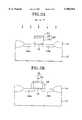
- FIG. 1shows a conventional MOSFET structure in accordance with the self-aligned silicide formation method.
- an active regionis defined by two device isolation oxides.
- Gate 4 of polycrystalline silicon(hereinafeter referred to as "polysilicon") overlying gate oxide 3is formed on a selected portion of the active region of the substrate 1.
- Lightly doped impurity regions 5are selectively formed in the substrate 1 at both sides of the gate 4 by ion implantation.
- Spacers 6 of silicon dioxide(SiO 2 )are formed on side walls of the gate 4 by a known method.
- heavily doped impurity regions of source 7a and drain 7bare formed by ion implantation of high concentration and subsequent annealing.
- metal filmis deposited at a selected thickness on the whole surface of the substrate 1. Thereafter, the substrate 1 is then annealed at a selected temperature, so as to react the deposited metal film with the underlying silicon, whereby metal silicide film 8 is formed. Thereafter, metal or metal compound which does not react with the underlying silicon are removed by selective etch.
- the above-described self-aligned silicide formation methodare useful in deep sub-micron MOSFETs.
- Titanium disilicide(TiSi 2 )has been widely used in such MOSFET structure because of its low resistivity.
- titanium used for the formation of the titanium disilicidehas high reactivity with silicon dioxide (SiO 2 ), it comes to be frequently reacted with the silicon dioxide, thereby forming a titanium silicide film on the device isolation oxide where titanium silicide need not be formed.
- the unnecessary titanium silicide film formed on the spacers or the device isolation oxideelectrically connects the source, drain, and gate with each other, so that the MOSFET does not serve as switching element.
- high stress by titanium silicide filmcauses defects to be generated in the source, drain and gate, electrical characteristic and reliability of the MOSFET are deteriorated.
- cobalt silicidefor titanium silicide.
- the cobalt silicidehowever needs a large amount of silicon for the formation thereof to a desired thickness, so that it is difficult to form stable and shallow junction of source and drain.
- the heating of the cobalt silicide to a temperature above about 1,000° C.increases surface energy of the cobalt silicide grains.
- the high surface energyleads to an agglomeration of large silicide grains during the annealing process.
- the cobalt silicide film formed in accordance with the conventional methodhas a low flatness, so that its contact resistance with the underlying silicon increases.
- a semiconductor substratehaving exposed silicon portions on the surface thereof.
- the exposed siliconis either single crystalline silicon or polycrystalline silicon, and may include junction regions in which N type or P type impurity such as arsenic, phosphorous, or boron is formed.
- Niobium and cobaltare sequentially deposited on the exposed silicon portions by electron-beam evaporation technique. Afterwards, annealing step is performed to form a cobalt silicide film on the exposed silicon portions.
- a method for fabricating a MOSFETcomprises the steps of: providing a semiconductor substrate in which device isolation oxides are formed; forming a gate including a gate insulator interposed between the gate and the substrate; forming source and drain regions in the substrate at both sides of the gate; forming spacers of insulator on both side walls of the gate; sequentially depositing niobium and cobalt on the entire surface of the resultant substrate; annealing the resultant substrate at a selected temperature, to form a cobalt silicide film on the source, drain, and gate; and removing residuals except the cobalt silicide.
- a method for fabricating a MOSFETcomprising the steps of: providing a semiconductor substrate in which device isolation oxides are formed; sequentially depositing silicon oxide layer, polysilicon layer, amorphous silicon layer, and anti-reflective layer on the semiconductor substrate, and patterning the deposited four layers, to form a gate and a gate insulator interposed between the gate and the substrate; implanting an N-type impurity at a low concentration into the substrate including the gate, to form lightly doped regions in the substrate at both sides of the gate; forming spacers of insulator on both side walls of the gate; removing the anti-reflectivelayer; implanting the N-type impurity into the substrate, at a concentration higher than that of the lightly doped regions to form source and drain regions; sequentially depositing niobium and cobalt on the resultant substrate to form source and drain regions; annealing the resultant substrate at a selected temperature, to form a cobalt silicide film on
- FIG. 1shows a conventional MOSFET structure in accordance with the self-aligned silicide formation method
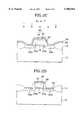
- FIGS. 2A-2Dare cross-sectional views for explaining the fabricating method of an MOSFET in accordance with a specific embodiment of the present invention.
- FIGS. 2A-2Dare cross-sectional views for explaining the fabricating method of an MOSFET in accordance with a specific embodiment of the present invention.
- a semiconductor substrate 12which can be composed of a bulk type silicon substrate or a silicon on insulator(SOI) substrate comprising a handling wafer, a buried insulating layer formed on the handling wafer and a silicon layer formed on the buried insulating layer.
- the SOI substrateis prepared by either bonding technique or separation by implanted oxygen(SIMOX) technique.
- SIMOXimplanted oxygen
- a first silicon wafer having an insulating layer formed thereon and a handling waferare prepared.
- the first silicon waferis attached to the handling wafer such that the insulating layer of the first silicon wafer faces the surface of the handling wafer.
- the silicon layer of the first silicon waferis polished to a selected thickness, resulting in a layer for the formation of devices.
- oxygen ions for the formation of the buried insulating layerare deeply implanted into a silicon wafer to form a buried insulating layer.
- a device isolation oxide 14, normally made of SiO 2is formed at selected portions of the substrate 12 by a well-known local oxidation of silicon(LOCOS) method, to define active regions where semiconductor devices are formed.
- LOCSlocal oxidation of silicon
- gate oxide 16 and gate 40silicon oxide, polysilicon, amorphous silicon, and anti-reflectivelayers are sequentially deposited in the order named on the substrate 12 at respective selected thickness and are patterned.
- the gate 40consists of a polysilicon pattern 18 and a amorphous pattern 20, but the amorphous pattern 20 may be omitted.
- the patterned anti-reflectivelayer 22is to prevent deterioration of photoresist mask due to the reflection of incident light for the patterning of photoresist film as coated on the above-mentioned four layers, but may be omitted.
- the patterned polysilicon18
- N-impurity or P-impurity doped polysiliconcan be used.
- the patterned amorphous silicon 20is preferably formed at a thickness of about 100 to 500 ⁇ .
- lightly doped impurity regionsmay be provided in the substrate 12 at both sides of the gate 40.
- N-impuritysuch as arsenic or phosphorous is implanted at a selected impurity concentration into the entire surface of the substrate 12 including the gate 40, thereby forming N - impurity doped regions 24a, 24b of low concentration.
- spacers 28made of silicon dioxide.
- the spacers 28are formed by depositing silicon dioxde at a thickness of 2000-3000 ⁇ by a chemical vapor deposition on the entire surface of the substrate 12 including the gate 40 and afterwards performing blanket etch until the silicon dioxide on the source 24a and drain 24b and the anti-reflectivelayer 22 are completely removed. At this time, the anti-reflectivelayer 22 is also removed. The above-mentioned anti-reflectivelayer 22 may be removed before the formation of the spacers 28.
- N + impurity doped regions 30a and 30b of high concentrationwhich are generally referred to as source and drain, are formed in the silicon substrate 12 by implanting N-type impurity ions of high concentration into the entire surface of the substrate 12.
- Niobium film 32 with about 200-500 ⁇ thickness and cobalt film 34 with about 200-500 ⁇ thicknessare sequentially deposited on the entire surface of the substrate 12 by electron-beam evaporation technique. At this time, pressure of a chamber for the deposition of the niobium film 32 and the cobalt film 34 must be maintained below 1 ⁇ 10 -7 Torr such that the metal films as deposited have superior qualities.
- the substrate resulting from the above mentioned stepsis thermally annealed in a temperature range of 800-900° C., in nitrogen atmosphere, thereby forming crystalline cobalt silicide film 36 on the source, drain, and gate regions.
- the thermal annealcontinues to proceed until the amorphous silicon 20 is completely consumed for the formation of the cobalt silicide film 22.
- residualssuch as Nb 2 O 5 , a compound of Co and Nb, and cobalt-rich silicide other than the cobalt disilicide(CoSi 2 ) are removed by selective etch.
- Silicon dioxide(SiO 2 )has Gibb's free energy Gf of about -204.7 Kcal/mol, while Nb 2 O 5 has Gibb's free energy of about -422.1 Kcal/mol.
- the Gibb's free energy of the Nb 2 O 5is larger than that of the silicon dioxide.
- Niobium disilicide(NbSi 2 )is formed at a temperature of about 650° C. relatively higher than the formation temperature of CoSi 2 .
- an activation energy for CoSi 2is about 1.5-2.0 eV, and that for NbSi 2 is about 2.7 eV.
- NbSi 2is hardly formed in case that a temperature for the thermal anneal is maintained at about 550° C.
- a small amount of silicon atomsare diffused into niobium film.
- niobium atomsreact easily with oxygen atoms compared to silicon atoms due to its high oxidation characteristic.
- oxidation degree of niobiumis the highest of metal atoms except tantalum, oxidation of niobium preferentially occurs.
- niobiumhas a high reactivity with cobalt, a reaction between niobium and cobalt is abruptly occurred, to create a small amount of a ternary compound of niobium, cobalt, and silicon.
- the ternary compoundreacts with the overlying residual cobalt, thereby forming cobalt silicide such as CoSi and/or CoSi 2 .
- NbSi 2is hardly formed at a temperature of about 550° C.
- intermediate phasessuch as Nb 2 O 5 , the compound of Nb and Co created during silicidation of cobalt and silicon serve as a barrier against abrupt interdiffusion, thereby forming a superior, good quality, stable cobalt disilicide.
- niobium film disposed between cobalt and silicon during the silicidation processprevents outdiffusion of the doped impurities toward the cobalt silicide film being formed, so that it is possible to obtain shallow, stable junctions.
- the present inventionprovides the following effects.
- amount of silicon used in forming the cobalt disilicideis relatively small, thereby facilitating shallow junction to be formed.
- surface energy of the cobalt silicide grainsdoes not increase, so that an agglomeration of large silicide grains does not occur.
- penetration of grains into the junction regions of source and draindecreases, an epitaxial regrowth of silicon between the silicide grains does not occur. As a result, leakage currents of such silicided junctions are decreased.
- substratemay be made of either single crystalline silicon or polysilicon, and may include junction regions in which N type or P type impurity such as arsenic, phosphorous, or boron is doped.
Landscapes
- Engineering & Computer Science (AREA)
- Physics & Mathematics (AREA)
- Condensed Matter Physics & Semiconductors (AREA)
- General Physics & Mathematics (AREA)
- Manufacturing & Machinery (AREA)
- Computer Hardware Design (AREA)
- Microelectronics & Electronic Packaging (AREA)
- Power Engineering (AREA)
- Chemical & Material Sciences (AREA)
- Chemical Kinetics & Catalysis (AREA)
- Electrodes Of Semiconductors (AREA)
- Insulated Gate Type Field-Effect Transistor (AREA)
Abstract
Description
Claims (32)
Applications Claiming Priority (2)
| Application Number | Priority Date | Filing Date | Title |
|---|---|---|---|
| KR1019960072822AKR100220253B1 (en) | 1996-12-27 | 1996-12-27 | Method of manufacturing mosfet |
| KR96-72822 | 1996-12-27 |
Publications (1)
| Publication Number | Publication Date |
|---|---|
| US5904564Atrue US5904564A (en) | 1999-05-18 |
Family
ID=19491203
Family Applications (1)
| Application Number | Title | Priority Date | Filing Date |
|---|---|---|---|
| US08/991,668Expired - Fee RelatedUS5904564A (en) | 1996-12-27 | 1997-12-16 | Method for fabricating MOSFET having cobalt silicide film |
Country Status (3)
| Country | Link |
|---|---|
| US (1) | US5904564A (en) |
| JP (1) | JPH10284728A (en) |
| KR (1) | KR100220253B1 (en) |
Cited By (17)
| Publication number | Priority date | Publication date | Assignee | Title |
|---|---|---|---|---|
| US5946598A (en)* | 1996-11-18 | 1999-08-31 | United Microelectronics Corporation | Process of fabricating metal gate electrode |
| US6063704A (en)* | 1999-08-02 | 2000-05-16 | National Semiconductor Corporation | Process for incorporating silicon oxynitride DARC layer into formation of silicide polysilicon contact |
| US6165902A (en)* | 1998-11-06 | 2000-12-26 | Advanced Micro Devices, Inc. | Low resistance metal contact technology |
| US6171959B1 (en)* | 1998-01-20 | 2001-01-09 | Motorola, Inc. | Method for making a semiconductor device |
| US6204177B1 (en)* | 1998-11-04 | 2001-03-20 | Advanced Micro Devices, Inc. | Method of forming junction leakage free metal silicide in a semiconductor wafer by alloying refractory metal |
| US6245682B1 (en)* | 1999-03-11 | 2001-06-12 | Taiwan Semiconductor Manufacturing Company | Removal of SiON ARC film after poly photo and etch |
| US6326289B1 (en)* | 1998-08-24 | 2001-12-04 | Texas Instruments Incorporated | Method of forming a silicide layer using a pre-amorphization implant which is blocked from source/drain regions by a layer of photoresist |
| US6346477B1 (en) | 2001-01-09 | 2002-02-12 | Research Foundation Of Suny - New York | Method of interlayer mediated epitaxy of cobalt silicide from low temperature chemical vapor deposition of cobalt |
| WO2002023615A1 (en)* | 2000-09-11 | 2002-03-21 | Ultratech Stepper, Inc. | Method for annealing using partial absorber layer exposed to radiant energy and article made with partial absorber layer |
| US6559018B1 (en) | 2002-01-18 | 2003-05-06 | Taiwan Semiconductor Manufacturing Company | Silicon implant in a salicided cobalt layer to reduce cobalt-silicon agglomeration |
| US6593223B1 (en) | 1998-06-01 | 2003-07-15 | United Microelectronics Corporation | Method of forming dual damascene structure |
| US6680248B2 (en) | 1998-06-01 | 2004-01-20 | United Microelectronics Corporation | Method of forming dual damascene structure |
| US6743721B2 (en) | 2002-06-10 | 2004-06-01 | United Microelectronics Corp. | Method and system for making cobalt silicide |
| US6767812B2 (en)* | 2001-06-14 | 2004-07-27 | Oki Electric Industry Co., Ltd. | Method of forming CVD titanium film |
| CN1295760C (en)* | 2003-06-16 | 2007-01-17 | 台湾积体电路制造股份有限公司 | Method of forming metal silicide |
| US7482217B1 (en) | 2007-12-03 | 2009-01-27 | Spansion Llc | Forming metal-semiconductor films having different thicknesses within different regions of an electronic device |
| CN113454755A (en)* | 2019-02-19 | 2021-09-28 | 应用材料公司 | Polysilicon liner |
Families Citing this family (6)
| Publication number | Priority date | Publication date | Assignee | Title |
|---|---|---|---|---|
| JP2008060594A (en)* | 1997-11-17 | 2008-03-13 | Toshiba Corp | Manufacturing method of semiconductor device |
| KR100524874B1 (en)* | 1998-06-10 | 2006-02-20 | 엘지.필립스 엘시디 주식회사 | Crystallization Method of Amorphous Silicon Thin Film |
| KR100315451B1 (en)* | 1999-04-13 | 2001-11-28 | 황인길 | Method for forming gate electrode and salicide contact of semiconductor devices |
| KR100763898B1 (en) | 2003-08-02 | 2007-10-05 | 삼성전자주식회사 | Semiconductor device manufacturing method and semiconductor device manufactured thereby |
| JP5880243B2 (en)* | 2012-04-18 | 2016-03-08 | 富士通セミコンダクター株式会社 | Semiconductor device and manufacturing method thereof |
| CN110942984B (en)* | 2018-09-25 | 2022-04-01 | 长鑫存储技术有限公司 | Preparation method of cobalt silicide film |
Citations (5)
| Publication number | Priority date | Publication date | Assignee | Title |
|---|---|---|---|---|
| US4378628A (en)* | 1981-08-27 | 1983-04-05 | Bell Telephone Laboratories, Incorporated | Cobalt silicide metallization for semiconductor integrated circuits |
| US5047367A (en)* | 1990-06-08 | 1991-09-10 | Intel Corporation | Process for formation of a self aligned titanium nitride/cobalt silicide bilayer |
| US5510295A (en)* | 1993-10-29 | 1996-04-23 | International Business Machines Corporation | Method for lowering the phase transformation temperature of a metal silicide |
| US5780361A (en)* | 1995-06-23 | 1998-07-14 | Nec Corporation | Salicide process for selectively forming a monocobalt disilicide film on a silicon region |
| US5780362A (en)* | 1996-06-04 | 1998-07-14 | Wang; Qingfeng | CoSi2 salicide method |
- 1996
- 1996-12-27KRKR1019960072822Apatent/KR100220253B1/ennot_activeExpired - Fee Related
- 1997
- 1997-12-16USUS08/991,668patent/US5904564A/ennot_activeExpired - Fee Related
- 1997-12-24JPJP9366428Apatent/JPH10284728A/enactivePending
Patent Citations (5)
| Publication number | Priority date | Publication date | Assignee | Title |
|---|---|---|---|---|
| US4378628A (en)* | 1981-08-27 | 1983-04-05 | Bell Telephone Laboratories, Incorporated | Cobalt silicide metallization for semiconductor integrated circuits |
| US5047367A (en)* | 1990-06-08 | 1991-09-10 | Intel Corporation | Process for formation of a self aligned titanium nitride/cobalt silicide bilayer |
| US5510295A (en)* | 1993-10-29 | 1996-04-23 | International Business Machines Corporation | Method for lowering the phase transformation temperature of a metal silicide |
| US5780361A (en)* | 1995-06-23 | 1998-07-14 | Nec Corporation | Salicide process for selectively forming a monocobalt disilicide film on a silicon region |
| US5780362A (en)* | 1996-06-04 | 1998-07-14 | Wang; Qingfeng | CoSi2 salicide method |
Cited By (27)
| Publication number | Priority date | Publication date | Assignee | Title |
|---|---|---|---|---|
| US5946598A (en)* | 1996-11-18 | 1999-08-31 | United Microelectronics Corporation | Process of fabricating metal gate electrode |
| US6171959B1 (en)* | 1998-01-20 | 2001-01-09 | Motorola, Inc. | Method for making a semiconductor device |
| US6680248B2 (en) | 1998-06-01 | 2004-01-20 | United Microelectronics Corporation | Method of forming dual damascene structure |
| US6593223B1 (en) | 1998-06-01 | 2003-07-15 | United Microelectronics Corporation | Method of forming dual damascene structure |
| US6326289B1 (en)* | 1998-08-24 | 2001-12-04 | Texas Instruments Incorporated | Method of forming a silicide layer using a pre-amorphization implant which is blocked from source/drain regions by a layer of photoresist |
| US6204177B1 (en)* | 1998-11-04 | 2001-03-20 | Advanced Micro Devices, Inc. | Method of forming junction leakage free metal silicide in a semiconductor wafer by alloying refractory metal |
| US6369429B1 (en) | 1998-11-06 | 2002-04-09 | Advanced Micro Devices, Inc. | Low resistance composite contact structure utilizing a reaction barrier layer under a metal layer |
| US6165902A (en)* | 1998-11-06 | 2000-12-26 | Advanced Micro Devices, Inc. | Low resistance metal contact technology |
| US6245682B1 (en)* | 1999-03-11 | 2001-06-12 | Taiwan Semiconductor Manufacturing Company | Removal of SiON ARC film after poly photo and etch |
| US6063704A (en)* | 1999-08-02 | 2000-05-16 | National Semiconductor Corporation | Process for incorporating silicon oxynitride DARC layer into formation of silicide polysilicon contact |
| WO2002023615A1 (en)* | 2000-09-11 | 2002-03-21 | Ultratech Stepper, Inc. | Method for annealing using partial absorber layer exposed to radiant energy and article made with partial absorber layer |
| US6346477B1 (en) | 2001-01-09 | 2002-02-12 | Research Foundation Of Suny - New York | Method of interlayer mediated epitaxy of cobalt silicide from low temperature chemical vapor deposition of cobalt |
| US6767812B2 (en)* | 2001-06-14 | 2004-07-27 | Oki Electric Industry Co., Ltd. | Method of forming CVD titanium film |
| US6559018B1 (en) | 2002-01-18 | 2003-05-06 | Taiwan Semiconductor Manufacturing Company | Silicon implant in a salicided cobalt layer to reduce cobalt-silicon agglomeration |
| US6878627B1 (en) | 2002-06-10 | 2005-04-12 | United Microelectronics Corporation | Semiconductor device with cobalt silicide contacts and method of making the same |
| US6743721B2 (en) | 2002-06-10 | 2004-06-01 | United Microelectronics Corp. | Method and system for making cobalt silicide |
| US20050176248A1 (en)* | 2002-06-10 | 2005-08-11 | Water Lur | Semiconductor device with cobalt silicide contacts |
| US20050179139A1 (en)* | 2002-06-10 | 2005-08-18 | Water Lur | Semiconductor device with cobalt silicide contacts |
| US6943110B1 (en) | 2002-06-10 | 2005-09-13 | United Microelectronics, Corp. | Wafer processing apparatus and methods for depositing cobalt silicide |
| US20060014388A1 (en)* | 2002-06-10 | 2006-01-19 | Water Lur | Wafer processing apparatus & methods for depositing cobalt silicide |
| CN1295760C (en)* | 2003-06-16 | 2007-01-17 | 台湾积体电路制造股份有限公司 | Method of forming metal silicide |
| US7482217B1 (en) | 2007-12-03 | 2009-01-27 | Spansion Llc | Forming metal-semiconductor films having different thicknesses within different regions of an electronic device |
| US20090140325A1 (en)* | 2007-12-03 | 2009-06-04 | Spansion Llc | Forming metal-semiconductor films having different thicknesses within different regions of an electronic device |
| US7880221B2 (en) | 2007-12-03 | 2011-02-01 | Spansion Llc | Forming metal-semiconductor films having different thicknesses within different regions of an electronic device |
| CN113454755A (en)* | 2019-02-19 | 2021-09-28 | 应用材料公司 | Polysilicon liner |
| US11170990B2 (en)* | 2019-02-19 | 2021-11-09 | Applied Materials, Inc. | Polysilicon liners |
| TWI831926B (en)* | 2019-02-19 | 2024-02-11 | 美商應用材料股份有限公司 | Polysilicon liners |
Also Published As
| Publication number | Publication date |
|---|---|
| KR100220253B1 (en) | 1999-09-15 |
| KR19980053694A (en) | 1998-09-25 |
| JPH10284728A (en) | 1998-10-23 |
Similar Documents
| Publication | Publication Date | Title |
|---|---|---|
| US5904564A (en) | Method for fabricating MOSFET having cobalt silicide film | |
| US5241193A (en) | Semiconductor device having a thin-film transistor and process | |
| JP2978736B2 (en) | Method for manufacturing semiconductor device | |
| US5767004A (en) | Method for forming a low impurity diffusion polysilicon layer | |
| KR100352758B1 (en) | Semiconductor device and method for manufacturing the same | |
| US5970352A (en) | Field effect transistor having elevated source and drain regions and methods for manufacturing the same | |
| US6765273B1 (en) | Device structure and method for reducing silicide encroachment | |
| KR100362751B1 (en) | Contact hole and method for forming the semiconductor device | |
| US6777759B1 (en) | Device structure and method for reducing silicide encroachment | |
| US5496750A (en) | Elevated source/drain junction metal oxide semiconductor field-effect transistor using blanket silicon deposition | |
| US5744395A (en) | Low resistance, self-aligned, titanium silicide structures, using a single rapid thermal anneal procedure | |
| US7144798B2 (en) | Semiconductor memory devices having extending contact pads and related methods | |
| US5391508A (en) | Method of forming semiconductor transistor devices | |
| US5103272A (en) | Semiconductor device and a method for manufacturing the same | |
| US6329277B1 (en) | Method of forming cobalt silicide | |
| US20050130380A1 (en) | Semiconductor device structures including metal silicide interconnects and dielectric layers at substantially the same fabrication level | |
| EP0603360B1 (en) | Methods of forming a local interconnect and a high resistor polysilicon load | |
| EP0404372B1 (en) | Method for forming polycrystalline silicon contacts | |
| US5858846A (en) | Salicide integration method | |
| US6765269B2 (en) | Conformal surface silicide strap on spacer and method of making same | |
| US6255181B1 (en) | Method for fabricating MOS semiconductor device having salicide region and LDD structure | |
| JPH08213610A (en) | Field effect type semiconductor device and method of manufacturing the same | |
| US6221760B1 (en) | Semiconductor device having a silicide structure | |
| US6287911B1 (en) | Semiconductor device with silicide layers and fabrication method thereof | |
| US6653227B1 (en) | Method of cobalt silicidation using an oxide-Titanium interlayer |
Legal Events
| Date | Code | Title | Description |
|---|---|---|---|
| AS | Assignment | Owner name:HYUNDAI ELECTRONICS INDUSTRIES CO., LTD., KOREA, R Free format text:ASSIGNMENT OF ASSIGNORS INTEREST;ASSIGNOR:PARK, SANG-HOON;REEL/FRAME:009469/0571 Effective date:19971111 | |
| FEPP | Fee payment procedure | Free format text:PAYOR NUMBER ASSIGNED (ORIGINAL EVENT CODE: ASPN); ENTITY STATUS OF PATENT OWNER: LARGE ENTITY | |
| CC | Certificate of correction | ||
| FPAY | Fee payment | Year of fee payment:4 | |
| AS | Assignment | Owner name:HYNIX SEMICONDUCTOR INC., KOREA, REPUBLIC OF Free format text:CHANGE OF NAME;ASSIGNOR:HYUNDAI ELECTRONICS INDUSTRIES CO., LTD.;REEL/FRAME:015242/0899 Effective date:20010329 | |
| AS | Assignment | Owner name:MAGNACHIP SEMICONDUCTOR, LTD., KOREA, REPUBLIC OF Free format text:ASSIGNMENT OF ASSIGNORS INTEREST;ASSIGNOR:HYNIX SEMICONDUCTOR, INC.;REEL/FRAME:016216/0649 Effective date:20041004 | |
| REMI | Maintenance fee reminder mailed | ||
| LAPS | Lapse for failure to pay maintenance fees | ||
| STCH | Information on status: patent discontinuation | Free format text:PATENT EXPIRED DUE TO NONPAYMENT OF MAINTENANCE FEES UNDER 37 CFR 1.362 | |
| FP | Lapsed due to failure to pay maintenance fee | Effective date:20070518 |