US5903010A - Quantum wire switch and switching method - Google Patents
Quantum wire switch and switching methodDownload PDFInfo
- Publication number
- US5903010A US5903010AUS08/959,887US95988797AUS5903010AUS 5903010 AUS5903010 AUS 5903010AUS 95988797 AUS95988797 AUS 95988797AUS 5903010 AUS5903010 AUS 5903010A
- Authority
- US
- United States
- Prior art keywords
- stub
- length
- quantum
- switch
- output
- Prior art date
- Legal status (The legal status is an assumption and is not a legal conclusion. Google has not performed a legal analysis and makes no representation as to the accuracy of the status listed.)
- Expired - Lifetime
Links
- 238000000034methodMethods0.000titleabstractdescription7
- 239000002800charge carrierSubstances0.000claimsabstractdescription39
- 239000004020conductorSubstances0.000claimsdescription27
- 239000000969carrierSubstances0.000claimsdescription15
- 239000000758substrateSubstances0.000claimsdescription10
- JBRZTFJDHDCESZ-UHFFFAOYSA-NAsGaChemical compound[As]#[Ga]JBRZTFJDHDCESZ-UHFFFAOYSA-N0.000claimsdescription7
- 229910001218Gallium arsenideInorganic materials0.000claimsdescription5
- FTWRSWRBSVXQPI-UHFFFAOYSA-Nalumanylidynearsane;gallanylidynearsaneChemical compound[As]#[Al].[As]#[Ga]FTWRSWRBSVXQPI-UHFFFAOYSA-N0.000claimsdescription5
- 239000002322conducting polymerSubstances0.000claimsdescription3
- 229920001940conductive polymerPolymers0.000claimsdescription3
- OKTJSMMVPCPJKN-UHFFFAOYSA-NCarbonChemical compound[C]OKTJSMMVPCPJKN-UHFFFAOYSA-N0.000claimsdescription2
- 239000002041carbon nanotubeSubstances0.000claimsdescription2
- 229910021393carbon nanotubeInorganic materials0.000claimsdescription2
- 150000004291polyenesChemical class0.000claimsdescription2
- 230000005428wave functionEffects0.000description34
- 230000005540biological transmissionEffects0.000description17
- 230000001902propagating effectEffects0.000description11
- 230000000694effectsEffects0.000description8
- 239000004065semiconductorSubstances0.000description8
- 239000002245particleSubstances0.000description7
- 230000010363phase shiftEffects0.000description6
- 230000001066destructive effectEffects0.000description5
- 230000000737periodic effectEffects0.000description5
- 230000005639quantum mechanical waveEffects0.000description3
- 238000013459approachMethods0.000description2
- 239000000470constituentSubstances0.000description2
- 230000001419dependent effectEffects0.000description2
- 230000005284excitationEffects0.000description2
- 230000033001locomotionEffects0.000description2
- 238000004519manufacturing processMethods0.000description2
- 239000011159matrix materialSubstances0.000description2
- 230000003287optical effectEffects0.000description2
- 230000005610quantum mechanicsEffects0.000description2
- 230000004044responseEffects0.000description2
- 238000000638solvent extractionMethods0.000description2
- XUIMIQQOPSSXEZ-UHFFFAOYSA-NSiliconChemical compound[Si]XUIMIQQOPSSXEZ-UHFFFAOYSA-N0.000description1
- 229910052782aluminiumInorganic materials0.000description1
- XAGFODPZIPBFFR-UHFFFAOYSA-NaluminiumChemical compound[Al]XAGFODPZIPBFFR-UHFFFAOYSA-N0.000description1
- 230000008859changeEffects0.000description1
- 238000000354decomposition reactionMethods0.000description1
- 239000012212insulatorSubstances0.000description1
- 230000002452interceptive effectEffects0.000description1
- 239000000463materialSubstances0.000description1
- 230000007246mechanismEffects0.000description1
- 229910052751metalInorganic materials0.000description1
- 239000002184metalSubstances0.000description1
- 238000013021overheatingMethods0.000description1
- 229910052710siliconInorganic materials0.000description1
- 239000010703siliconSubstances0.000description1
- 239000007787solidSubstances0.000description1
- 239000000126substanceSubstances0.000description1
Images


Classifications
- B—PERFORMING OPERATIONS; TRANSPORTING
- B82—NANOTECHNOLOGY
- B82Y—SPECIFIC USES OR APPLICATIONS OF NANOSTRUCTURES; MEASUREMENT OR ANALYSIS OF NANOSTRUCTURES; MANUFACTURE OR TREATMENT OF NANOSTRUCTURES
- B82Y10/00—Nanotechnology for information processing, storage or transmission, e.g. quantum computing or single electron logic
- H—ELECTRICITY
- H10—SEMICONDUCTOR DEVICES; ELECTRIC SOLID-STATE DEVICES NOT OTHERWISE PROVIDED FOR
- H10D—INORGANIC ELECTRIC SEMICONDUCTOR DEVICES
- H10D48/00—Individual devices not covered by groups H10D1/00 - H10D44/00
- H10D48/383—Quantum effect devices, e.g. of devices using quantum reflection, diffraction or interference effects
- H—ELECTRICITY
- H10—SEMICONDUCTOR DEVICES; ELECTRIC SOLID-STATE DEVICES NOT OTHERWISE PROVIDED FOR
- H10D—INORGANIC ELECTRIC SEMICONDUCTOR DEVICES
- H10D62/00—Semiconductor bodies, or regions thereof, of devices having potential barriers
- H10D62/80—Semiconductor bodies, or regions thereof, of devices having potential barriers characterised by the materials
- H10D62/81—Semiconductor bodies, or regions thereof, of devices having potential barriers characterised by the materials of structures exhibiting quantum-confinement effects, e.g. single quantum wells; of structures having periodic or quasi-periodic potential variation
- H10D62/812—Single quantum well structures
- H10D62/813—Quantum wire structures
- Y—GENERAL TAGGING OF NEW TECHNOLOGICAL DEVELOPMENTS; GENERAL TAGGING OF CROSS-SECTIONAL TECHNOLOGIES SPANNING OVER SEVERAL SECTIONS OF THE IPC; TECHNICAL SUBJECTS COVERED BY FORMER USPC CROSS-REFERENCE ART COLLECTIONS [XRACs] AND DIGESTS
- Y10—TECHNICAL SUBJECTS COVERED BY FORMER USPC
- Y10S—TECHNICAL SUBJECTS COVERED BY FORMER USPC CROSS-REFERENCE ART COLLECTIONS [XRACs] AND DIGESTS
- Y10S977/00—Nanotechnology
- Y10S977/902—Specified use of nanostructure
- Y10S977/932—Specified use of nanostructure for electronic or optoelectronic application
- Y10S977/936—Specified use of nanostructure for electronic or optoelectronic application in a transistor or 3-terminal device
- Y—GENERAL TAGGING OF NEW TECHNOLOGICAL DEVELOPMENTS; GENERAL TAGGING OF CROSS-SECTIONAL TECHNOLOGIES SPANNING OVER SEVERAL SECTIONS OF THE IPC; TECHNICAL SUBJECTS COVERED BY FORMER USPC CROSS-REFERENCE ART COLLECTIONS [XRACs] AND DIGESTS
- Y10—TECHNICAL SUBJECTS COVERED BY FORMER USPC
- Y10S—TECHNICAL SUBJECTS COVERED BY FORMER USPC CROSS-REFERENCE ART COLLECTIONS [XRACs] AND DIGESTS
- Y10S977/00—Nanotechnology
- Y10S977/902—Specified use of nanostructure
- Y10S977/932—Specified use of nanostructure for electronic or optoelectronic application
- Y10S977/94—Specified use of nanostructure for electronic or optoelectronic application in a logic circuit
Definitions
- the present inventionrelates generally to electrical conductors and switches and more particularly to a quantum wire switch and a method of switching electrical current.
- wires and switchesare in widespread use in applications ranging from industrial motor controls to ordinary house wiring to high-speed solid state logic in microcomputers.
- a wire that carries current for a given electrical devicemust be physically large enough to carry the quantity of current required by the device without overheating.
- wires and switchesshould be no larger than needed. The constraint of making wires and switches big enough to perform their functions and as small as possible to minimize size and cost is particularly critical in microprocessor fabrication because a very large number of wires and switches must fit into a very small space.
- An electric currentcan be defined as a flow of charge carriers through a conductor. Countless millions of charge carriers can fit on a cross-sectional slice of a typical conductor such as house wiring, and even at the small dimensions found in today's integrated circuits many charge carriers can fit across one conductor.
- the particle behavioris dominant in any object where the wavelength associated with the object, called the de Broglie wavelength, is much smaller than the other characteristic dimensions of the physical system in which the object is present. For all practical purposes, this means that an object large enough to be seen with the human eye will behave like a particle rather than like a wave. Newton's laws of motion describe the particle behavior of these objects.
- Quantum mechanicsis the study of systems that approach the size of the de Broglie wavelength where the wave nature of particles becomes dominant.
- the de Broglie wavelength associated with a charge carrier in a semiconductor such as gallium arsenideis of the order of ten nanometers (one nanometer is 10 -9 meters). If the conductor in which such a charge carrier is moving has a cross-section only slightly larger than the de Broglie wavelength of the particle, the wave behavior of the charge carrier will become dominant and will correctly predict what will happen to the charge carrier as it moves through the conductor.
- One aspect of the wave behavior of objectsis the occurrence of quantum interference effects.
- Quantum interference effectsare similar to interference effects observed in optical systems, such as interferometers and reflection gratings, but occur only for much smaller physical systems.
- optical systemssuch as interferometers and reflection gratings
- Quantum interference effectsare similar to interference effects observed in optical systems, such as interferometers and reflection gratings, but occur only for much smaller physical systems.
- the developing capability of fabricating smaller and smaller conductorshas allowed researchers to begin to investigate electrical devices whose operational characteristics are dependent upon the quantum interference effects of charge carriers.
- quantum wiresare long thin channels which confine charge carriers within a region of maximum transverse dimension comparable to the de Broglie wavelength of those charge carriers.
- quantum wirescan act as fermionic waveguides, in direct analogy to electromagnetic waveguides.
- the carriersIn order for the propagating modes of the quantum wire to maintain their quantum wave coherence along the length of the structure, it is necessary that the carriers enjoy “ballistic transport”. This means the carriers must not undergo decohering inelastic scattering events as they propagate through the structure. Due to improvements in achievable materials characteristics, simple quantum wire structures have been fabricated and tested, as reported, for example, by Ismail, Bagwell, Orlando, Antoniadis and Smith in the Proceedings of the IEEE, volume 79, page 1106 (1991).
- a means of controlling the conductance properties of the channelhas been implemented by making a channel with a variable length stub of quantum wire attached in the transverse dimension.
- the conductance of the channelis affected by reflected standing waves which are established in the stub. These standing waves interfere with the channel wave function. The interference effects are dependent upon the de Broglie wavelength of the carriers and the length of the stub.
- the channel and stubare fabricated as, for example, gallium arsenide (GaAs) channels in an aluminum gallium arsenide (AlGaAs) substrate, the length of the stub can be controlled by a bias voltage which varies a depletion region that determines the stub termination point.
- the conductance of the channel in an electron stub tuneris expected to be a periodic function of the stub length, and this is borne out by data descriptive of actual electron stub tuners (see Aihara, Yamamoto and Mizutani, International Electronic Devices Meeting, 1992).
- the electron stub tuner and other possible quantum wire structurescan be theoretically analyzed using a simple model wherein the wire channels are assumed to have negligible transverse spatial extent. This allows analysis of the structure by solving the one-dimensional Schrodinger's equation on a thin-wire network wherein the wavefunctions and boundary conditions are well-defined, as described in Ruedenberg and Scherr, Journal of Chemical Physics, vol. 21, page 1565 (1953).
- quantum wire structures of more complicated topologies than the electron stub tunercould be developed, it would be possible to create an entirely new class of electronic devices that would offer significant advantages over conventional devices in terms of smaller size, higher speed, and lower power consumption. Accordingly, it will be apparent that there is a need for quantum wire devices having more capabilities than the electron stub tuner.
- the present inventionprovides a fundamental electronic circuit device--a switch--implemented in a quantum wire structure.
- the switchoffers the higher speed and lower power consumption that will be required in computers and other appliances of the future.
- a quantum wireextends from an input to a first node and a second quantum wire extends from the input to a second node.
- a third quantum wireextends between the first and second nodes, the three quantum wires together defining a ring.
- a controllable-length quantum wire stubis connected to the first quantum wire.
- Charge carrierspropagate from the input around the ring.
- Quantum interferenceresults in local maxima and minima at various points around the ring.
- Setting the stub to a first lengthresults in a local maximum at the first node and a local minimum at the second node.
- the charge carrierscan propagate to an output at the first node but not to an output at the second node.
- Setting the stub to a second lengthchanges the locations of the local maxima and minima, and the charge carriers can propagate to the output at the second node but not the output at the first node.
- a second controllable-length stubis connected to the first quantum wire spaced apart from the first stub. Simultaneously setting both stubs to a common length results in cleaner switching.
- a simple binary NOT logic gateis implemented by applying a fixed input of electrical charge carriers to the input port of the switch as described above and structuring the control of the stub such that a logical ZERO sets the length of the stub to the first length and a logical ONE sets it to the second length. Taking the output from the first node with the sense that the presence of the electrical charge carriers is a logical ONE results in a logical ONE output when a logical ZERO is applied to control the stub, and vice versa.
- a simple binary AND logic gateis implemented such that a first logical ONE input applies a fixed input of electrical charge carriers to the input port of the switch as described above, and a first logical ZERO input removed the fixed input of electrical charge carriers from the input port of the switch.
- control of the stubis structured such that a second logical ZERO input sets the length of the stub to the first length and a second logical ONE input sets it to the second length. Taking the output from the first node with the sense that the presence of the electrical charge carriers is a logical ONE results in a logical ONE output only when a first logical ONE is applied to the input port and a second logical ONE is applied to the control stub.
- a method of switching an electric current according to the inventionincludes causing a current of electric charge carriers to propagate between first and second nodes on a conductor.
- an interferenceis generated such that the magnitude of the current is minimized at the first node and maximized at the second node.
- an interferenceis generated such that the magnitude of the current is minimized at the second node and maximized at the first node.
- FIG. 1Ais a schematic view of a straight quantum wire segment as known in the prior art.
- FIG. 1Bis a schematic view of a quantum wire segment including a 90 degree bend as known in the prior art.
- FIG. 1Cis a schematic view of a quantum wire junction as known in the prior art.
- FIG. 1Dis a schematic view of a quantum wire stub tuner as known in the prior art.
- FIG. 2is a schematic view depicting the structural topology of a single stub quantum switch according to the invention.
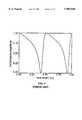
- FIG. 3is a graph depicting transmission phase shift as a function of stub length for an electron stub tuner as shown in FIG. 1D with an incident carrier energy of 1.5 times the cutoff energy of the lowest propagating mode.
- FIG. 4is a graph depicting transmission magnitude as a function of stub length for an electron stub tuner with an incident carrier energy of 1.5 times the cutoff energy of the lowest propagating mode.
- FIG. 5is similar to FIG. 1B showing partitioning of the quantum wire bend into three distinct physical regions for mode matching purposes.
- FIG. 6is similar to FIG. 1C showing partitioning of the quantum wire junction into four distinct physical regions for mode matching purposes.
- FIG. 7is similar to FIG. 2 showing decomposition of the quantum wire switch structure into ten straight wire segments and six junction regions.
- FIG. 8is a graph depicting the scattering probability to each of the two outputs as a function of stub length for the optimum geometry of the single stub quantum switch.
- FIG. 9is a contour plot of the magnitude of the quantum wavefunction over the single stub quantum switch geometry for a stub length corresponding to output 1 turned on and output 2 turned off.
- FIG. 10is a contour plot of the magnitude of the quantum wavefunction over the single stub quantum switch geometry for a stub length corresponding to output 2 turned on and output 1 turned off.
- FIG. 11is a schematic view depicting the structural topology of a double stub quantum switch according to the invention.
- FIG. 12is a graph depicting the scattering probability to each of the two outputs as a function of stub length for the optimum geometry of the double stub quantum switch.
- FIG. 13is a contour plot of the magnitude of the quantum wavefunction over the double stub quantum switch geometry for stub lengths corresponding to output 1 turned on and output 2 turned off.
- FIG. 14is a contour plot of the magnitude of the quantum wavefunction over the double stub quantum switch geometry for stub lengths corresponding to output 2 turned on and output 1 turned off.
- the inventionis embodied in a novel electrical switch and a switching method based upon quantum wire components.
- the switchcontrols the conductance between an input and a pair of outputs by varying the wavefunction phase shift around a quantum wire ring connecting the external nodes.
- the phase shiftis controlled using an electron stub tuner.
- the inventionis based upon the concept that scaling of structures down to dimensions smaller than the elastic and inelastic mean free paths of the charge carriers causes the carrier transport to become ballistic. For such systems, the quantum mechanical wave nature of the charge carriers becomes manifest. This allows new device topologies that can exploit the quantum mechanical wave nature of the charge carriers to generate useful device functionality.
- the quantum switch according to the inventionis smaller, faster, and requires far less electrical current to operate than transistor switches in use today. These properties make the switch according to the invention ideal for use in microprocessors and other integrated circuits.
- the smaller sizemeans that more of the switches can be formed in a given area of substrate than would be possible with transistors.
- Lower current usagemeans that less heat is generated by circuits utilizing the switches according to the invention than a comparable transistor-based circuit.
- the faster switching speedmeans that switch-based circuits will operate with more speed than is possible with comparable transistor-based circuits.
- FIGS. 1A, 1B, 1C and 1Ddepict components that have previously been scaled down to such a point that the quantum mechanical wave nature of the charge carriers has become manifest.
- FIG. 1Adepicts a straight quantum wire segment 1.
- FIG. 1Bdepicts a quantum wire having right-angle wire bend 2.
- FIG. 1Cdepicts a quantum wire junction 3 in which one end of a first quantum wire is joined to a second quantum wire such that the angle between the first and second quantum wires forms a right angle.
- FIG. 1Ddepicts an electron stub tuner 4 consisting of a segment of quantum wire which has a lateral quantum wire stub attached.
- GaAsgallium arsenide
- AlGaAsaluminum gallium arsenide
- the charge carriersare confined in the GaAs channels because GaAs has a lower bandgap than the Al GaAs substrate surrounding the channels.
- the componentscan be fabricated as semiconductor channels in many semiconductor substrates, as long as the difference in the bandgap between the channel and the substrate is sufficiently large.
- the quantum componentscan also be fabricated from elemental metal or metallic wires formed on a semiconductor or an insulator substrate, for example aluminum wires formed on a silicon substrate. Further, the quantum components can be fabricated from conjugated polyenes and other conducting polymers. Additionally, the quantum components can be fabricated from carbon nanotubes.
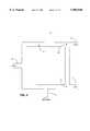
- FIG. 2depicts the structure of one preferred embodiment of the quantum switch according to the invention.
- the switchconsists of an input quantum wire 6 connected to a pair of output quantum wires 7, 8 by a quantum wire ring 9, with an attached electron stub tuner 10 on a segment of the ring.
- the switch 5allows the conductance between the input line 6 and the output lines 7, 8 to be controlled with an external switching voltage applied to the electron stub tuner 10.
- the charge carrier current incident on the input linehas two paths, one in each direction around the ring, to the nodes 11, 12 of the output lines.
- the width of the conductors that constitute the quantum wire ring 9approaches the de Broglie wavelength of the carries so the quantum wave nature of the carriers becomes dominant. As a result, the movement of the carriers around the quantum wire ring 9 is wavelike. A single carrier can thus propagate in either direction (clockwise path and counterclockwise path) around the ring, and can actually propagate in both directions simultaneously. Because waves are propagating in both directions, the phase of the quantum wavefunction along the two paths can cause constructive or destructive interference at various points around the ring.
- the location of the maximum constructive interferencecan be made to coincide with the first output node 11, while a location of the maximum destructive interference can be made to coincide with the second output node 12.
- the locations of the maximum constructive and destructive interferencecan be changed. If a proper electron stub tuner effective length is chosen, the location of the maximum constructive interference can be made to coincide with the second output node 12, while a location of the maximum destructive interference can be made to coincide with the first output node 11.
- the operation of the quantum wire switch according to the inventionrequires mathematical analysis of each of the quantum wire components 1, 2, 3, 4 shown in FIGS. 1A, 1B, 1C, and 1D, respectively.
- the operation of these quantum wire componentscan be understood by analogy to guided wave phenomena in microwave and optical devices.
- the electron stub tuner 4if the width of the quantum wires is adequately narrow, only the lowest transverse mode of the carriers in the conduction channel propagate.
- the electron stub tuner channel conductanceis a periodic function of the stub length, varying between zero (0) and one (1) in units of 2e 2 /, where e is the electron charge and is Planck's constant, due to the interference between the carrier waves propagating in the quantum wire and those reflected in the stub region.
- the length of the stubcan be controlled, for example, by applying a gate voltage which varies a semiconductor depletion region defining the end of the stub.
- the phase of the quantum wavefunction along the two paths (clockwise and counterclockwise) around the wire ring 9can cause constructive or destructive interference at the two output nodes 11, 12.
- This transmission probabilitycan be related to the carrier conductance by the quantum unit of conductance, 2e 2 /.
- the stub tunerhas a transmission characteristic which is a periodic function of its length. Both the quantum wavefunction transmission magnitude and phase exhibit this periodic behavior.
- FIG. 3is a plot of the transmission phase shift of an electron stub tuner for an incident carrier of energy 1.5 times the cutoff energy of the lowest propagating mode. The length of the electron stub tuner 10 is shown on the x-axis in units of wavelength ( ⁇ 0 ), and the transmission phase shift is shown on the y-axis in units of ⁇ .
- FIG. 4is a plot of the transmission magnitude of an electron stub tuner for an incident carrier of energy 1.5 times the cutoff energy of the lowest propagating mode. The length of the electron stub tuner 10 is shown on the x-axis in units of wavelength ( ⁇ 0 ), and the transmission magnitude is shown on the y-axis.
- This periodic behaviorallows the stub tuner to be used as an effective phase shifter for the quantum wavefunction on one branch of the structure of FIG. 2.
- the quantum interference around the ring structurecan be changed, allowing the carrier conductance to be switched from one output line to the other.
- the wavefunction in all straight wire segmentsis given as an expansion in a complete set of guided modes.
- the coefficients of the expansions in adjacent straight segmentsare linearly related to one another by demanding that the wavefunction and its first spatial derivative be continuous across the proximal connection region.
- the connection formulas for each of the quantum components 1, 2, 3, 4are detailed below. For these formulas, it is assumed that the carriers are governed by the time-independent Schrodinger wave equation in the effective mass approximation for the regions interior to the quantum wire components.
- the wavefunctionis constrained to be zero at the boundary edges of the conduction channels (hard wall approximation).
- the general solution for the guided modes in these straight segmentscan be written as an infinite sum over the complete set of guided modes ##EQU2## where x and y are the directions along and transverse to the wire propagation direction respectively, the subscript i identifies the particular wire segment, d is the lateral width of the wire, and the longitudinal wavevector ⁇ m is given by ##EQU3##
- the longitudinal wavevector, ⁇ mis real for open propagation channels and imaginary for closed propagation channels.
- the quantum wire bend 2can be broken up into three distinct regions as shown in FIG. 5.
- the three regionsinclude two straight wire segments W1 and W2 and a bend junction region J that connects the two straight wire segments.
- the two straight wire segments W1 and W2have wavefunction solutions given by ##EQU4## where the subscript numerals 1 and 2 specify the regions representing regions W1 and W2, respectively.
- the wavefunction within the bend junction region Jis chosen to be a sum of solutions of equation (1) that satisfy continuity of the wavefunction across the region boundaries 13 ##EQU5##
- connection formulas relating the wavefunction solutions in the two straight segments of the quantum wire bendare obtained by demanding continuity of the normal spatial derivatives across the boundaries 13 between each of the three regions ##EQU6##
- the quantum wire junction 3can be broken up into four distinct regions as shown in FIG. 6.
- the four regionsinclude three straight wire segments S1, S2 and S3 and an intersection region I that connects the three straight wire segments.
- the three straight wire segments S1, S2 and S3have wavefunction solutions given by ##EQU8## where the index i specifies the region and runs from 1 to 3 representing regions S1, S2, and S3 respectively.
- the wavefunction within the intersection region I of the junctionis chosen to be a sum of solutions of equation (1) that satisfy continuity of the wavefunction across the region boundaries 14 ##EQU9##
- connection formulas relating the wavefunction solutions in the three straight segments S1, S2 and S3 of the quantum wire junctionare obtained by demanding continuity of the normal spatial derivatives across each of the boundaries 14 between the four regions S1, S2, S3 and I ##EQU10##
- the electron stub tuner 4can also be broken up into four distinct regions S1, S2, S3 and I in the same way as described above and shown in FIG. 6 for the quantum wire junction.
- One of the quantum straight wire regions S3, however,is terminated at an effective length L.
- connection formulasrelating coefficients of the normal mode expansions of the quantum wavefunction for straight segments of quantum wire, can be applied to the topology of a quantum switch 5 described above.
- FIG. 7the structure of a quantum switch 5 is decomposed into ten constituent quantum wire segments 21-30 connected by six junction regions 31-36.
- the geometryis specified by the effective length of the stub tuner, L, and four independent length parameters, ⁇ A , ⁇ B , ⁇ C , and ⁇ D that define the length of four quantum straight wire segments 30, 22, 23, and 25, respectively. All dimensions are specified in units of the wire width, d. It should be noted that in the ten constituent quantum wire segments 21-30 are represented in the following equations by subscript numerals 1 through 10 respectively.
- the length parameters giving the greatest switching efficiency for the single electron stub tuner embodiment of a quantum switch 5can be calculated.
- FIG. 8shows a plot of the scattering probability to each of the two output lines as a function of effective stub length for this optimum geometry.
- the solid lineis a plot of the square of the magnitude of the coefficient of the normalized outgoing propagating mode on the first output line. This line peaks to a value of about 0.82
- the dashed lineis a plot of the analogous quantity for the second output line.
- This linereaches a low of about 0.06
- the conductance from the input line to the output lineshas a switching characteristic of better than 10:1. This indicates that this embodiment has the desired property of efficiently switching an effective electrical connection from one circuit branch to another by changing the effective length of the component stub tuner.
- FIG. 9is a contour plot of the magnitude of the quantum wavefunctions corresponding to the peak of the curve for the first output line shown in FIG. 8. The plot illustrates the large transmission probability from the input line 21 to the first output line 26 as well as the minimal transmission probability from the input line to output line 2.
- FIG. 10is a contour plot of the magnitude of the quantum wavefunction corresponding to the peak of the curve for the output line 2 shown in FIG. 8. A large transmission probability from the input line 21 to the second output line 28 as well as the minimal transmission probability from the input line to the first output line are illustrated.
- FIG. 11A second preferred embodiment of a quantum switch 37 according to the invention is depicted in FIG. 11.
- the switchconsists of an input quantum wire 38 connected to a pair of output quantum wires 39, 40 by a quantum wire ring 41, with a first electron stub tuner 42 attached on a segment of the ring, and a second electron stub tuner 43 attached on a segment of the ring.
- the second electron stub tunercan be placed at any point on the ring, but it is preferably adjacent to the first electron stub tuner and of the same effective length as the first electron stub tuner.
- the second electron stub tunercan also be driven by a second control voltage distinct from the first control voltage, but it is preferable that a single control voltage (not shown) controls both stub tuners.
- the geometry of the two electron stub tuner quantum switch 37can be specified using the length of the two stub tuners, L, and the five independent length parameters, ⁇ E , ⁇ F , ⁇ G , ⁇ H and ⁇ I that define the length of five quantum straight wire segments 44, 45, 46, 47 and 48, respectively. All dimensions are specified in units of the wire width, d
- FIG. 12shows a plot of the scattering probability to each of the two output lines as a function of effective stub length for this optimum geometry.
- the solid lineis a plot of the square of the magnitude of the coefficient of the normalized outgoing propagating mode on the first output line. This line reaches a low of about 0.00
- the dashed lineis a plot of the analogous quantity for the second output line.
- This linereaches a peak of about 0.95
- the efficiency of the scattering probability from the input line to the output lineshas increased over that of the single electron stub tuner quantum switch 5 from the maximum of roughly 80% to a maximum of over 95%.
- FIG. 13is a contour plot of the magnitude of the quantum wavefunctions corresponding to the peak of the curve for the first output line shown in FIG. 12. The plot illustrates the large transmission probability from the input line 38 to the first output line 39 as well as the minimal transmission probability from the input line to the second output line.
- FIG. 14is a contour plot of the magnitude of the quantum wavefunction corresponding to the peak of the curve for the second output line shown in FIG. 12. A large transmission probability from the input 38 to the second output line 40 as well as the minimal transmission probability from the input line to the first output line are illustrated.
- a simple binary NOT logic gatecan be implemented. This is accomplished by applying a fixed input of electrical charge carriers to the input 6 of the switch and structuring the control of the electron stub tuner 10 such that a logical ZERO sets the effective length of the stub to the first length and a logical ONE sets it to the second length. Taking the output from one of the output lines 7, 8 with the sense that the presence of the electrical charge carriers is a logical ONE results in a logical ONE output when a logical ZERO is applied to control the stub, and vice versa.
- a logical ZERO inputcan be defined as a control condition that sets the effective stub length to approximately 0.47 ⁇ 0 , where ⁇ 0 is the carrier wavelength along the propagation direction.
- a logical ONE inputcan similarly be defined as a control condition that sets the effective stub length to approximately 0.53 ⁇ 0 .
- a logical ZERO inputwould provide a logical ONE output at the first output line 7, and a logical ONE input would provide a logical ZERO output at the first output line.
- the structure of the double electron stub tuner quantum switch 37can be implemented as a simple binary NOT logic gate.
- a logical ZERO inputcan be defined as a control condition that sets the effective stub length to approximately 0.42 ⁇ 0 , where ⁇ 0 is the carrier wavelength along the propagation direction.
- a logical ONE inputcan similarly be defined as a control condition that sets the effective stub length to approximately 0.48 ⁇ 0 .
- a logical ZERO inputwould provide a logical ONE output at the second output line 40, and a logical ONE input would provide a logical ZERO output at the second output line.
- a simple binary AND logic gatecan be implemented. This is accomplished by defining the application of a fixed input of electrical charge carriers to the input 6 of the switch as a first logical ONE, and the absence of the fixed input to the input of the switch as a first logical ZERO.
- the control of the electron stub tuner 10is structured such that a second logical ZERO sets the effective length of the stub to the first length and a second logical ONE sets it to the second length.
- a second logical ZERO inputcan be defined as a control condition that sets the effective stub length to approximately 0.47 ⁇ 0 , where ⁇ 0 is the carrier wavelength along the propagation direction.
- a second logical ONE inputcan similarly be defined as a control condition that sets the effective stub length to approximately 0.53 ⁇ 0 .
- a second logical ZERO inputwould provide a logical ZERO output at the first output line 7, whether or not a first logical ONE is applied to the input 6.
- a second logical ONE inputwould provide a logical ZERO output at the first output line 7 only if there is also a first logical ONE applied to the input.
- the structure of the double electron stub tuner quantum switch 37can be implemented as a simple binary AND logic gate.
- a second logical ZERO inputcan be defined as a control condition that sets the effective stub length to approximately 0.42 ⁇ 0 , where ⁇ 0 is the carrier wavelength along the propagation direction.
- a second logical ONE inputcan similarly be defined as a control condition that sets the effective stub length to approximately 0.48 ⁇ 0 .
- a second logical ZERO inputwould provide a logical ZERO output at the second output line 40, whether or not a first logical ONE is applied to the input 38.
- a second logical ONE inputwould provide a logical ZERO output at the second output line 40 only if there is also a first logical ONE applied to the input 38.
- the above described quantum switch according to the inventionprovides a smaller, faster, and electrically more efficient switch than the transistor switches in use today. These properties make the invention ideal for use in microprocessors and other integrated circuits and it may eventually replace the transistor, just as the transistor replaced vacuum tubes.
Landscapes
- Engineering & Computer Science (AREA)
- Chemical & Material Sciences (AREA)
- Nanotechnology (AREA)
- Physics & Mathematics (AREA)
- Mathematical Physics (AREA)
- Theoretical Computer Science (AREA)
- Crystallography & Structural Chemistry (AREA)
- Junction Field-Effect Transistors (AREA)
Abstract
Description
A.sub.3n e.sup.iα.sbsp.n.sup.L +B.sub.3n e.sup.-iα.sbsp.n.sup.L =0. (18)
B.sub.6n =B.sub.8n =0 (20)
Claims (11)
Priority Applications (2)
| Application Number | Priority Date | Filing Date | Title |
|---|---|---|---|
| US08/959,887US5903010A (en) | 1997-10-29 | 1997-10-29 | Quantum wire switch and switching method |
| US09/228,214US6060724A (en) | 1997-10-29 | 1999-01-11 | Quantum wire logic gate |
Applications Claiming Priority (1)
| Application Number | Priority Date | Filing Date | Title |
|---|---|---|---|
| US08/959,887US5903010A (en) | 1997-10-29 | 1997-10-29 | Quantum wire switch and switching method |
Related Child Applications (1)
| Application Number | Title | Priority Date | Filing Date |
|---|---|---|---|
| US09/228,214DivisionUS6060724A (en) | 1997-10-29 | 1999-01-11 | Quantum wire logic gate |
Publications (1)
| Publication Number | Publication Date |
|---|---|
| US5903010Atrue US5903010A (en) | 1999-05-11 |
Family
ID=25502542
Family Applications (2)
| Application Number | Title | Priority Date | Filing Date |
|---|---|---|---|
| US08/959,887Expired - LifetimeUS5903010A (en) | 1997-10-29 | 1997-10-29 | Quantum wire switch and switching method |
| US09/228,214Expired - LifetimeUS6060724A (en) | 1997-10-29 | 1999-01-11 | Quantum wire logic gate |
Family Applications After (1)
| Application Number | Title | Priority Date | Filing Date |
|---|---|---|---|
| US09/228,214Expired - LifetimeUS6060724A (en) | 1997-10-29 | 1999-01-11 | Quantum wire logic gate |
Country Status (1)
| Country | Link |
|---|---|
| US (2) | US5903010A (en) |
Cited By (49)
| Publication number | Priority date | Publication date | Assignee | Title |
|---|---|---|---|---|
| US6340822B1 (en)* | 1999-10-05 | 2002-01-22 | Agere Systems Guardian Corp. | Article comprising vertically nano-interconnected circuit devices and method for making the same |
| US20020117659A1 (en)* | 2000-12-11 | 2002-08-29 | Lieber Charles M. | Nanosensors |
| US6512119B2 (en) | 2001-01-12 | 2003-01-28 | Hewlett-Packard Company | Bistable molecular mechanical devices with an appended rotor activated by an electric field for electronic switching, gating and memory applications |
| US6515325B1 (en)* | 2002-03-06 | 2003-02-04 | Micron Technology, Inc. | Nanotube semiconductor devices and methods for making the same |
| US6574130B2 (en) | 2001-07-25 | 2003-06-03 | Nantero, Inc. | Hybrid circuit having nanotube electromechanical memory |
| US20030199172A1 (en)* | 2001-07-25 | 2003-10-23 | Thomas Rueckes | Methods of nanotube films and articles |
| US6643165B2 (en) | 2001-07-25 | 2003-11-04 | Nantero, Inc. | Electromechanical memory having cell selection circuitry constructed with nanotube technology |
| US6706402B2 (en) | 2001-07-25 | 2004-03-16 | Nantero, Inc. | Nanotube films and articles |
| US6781166B2 (en) | 1999-07-02 | 2004-08-24 | President & Fellows Of Harvard College | Nanoscopic wire-based devices and arrays |
| US20040164289A1 (en)* | 2001-12-28 | 2004-08-26 | Nantero, Inc. | Electromechanical three-trace junction devices |
| US6784028B2 (en) | 2001-12-28 | 2004-08-31 | Nantero, Inc. | Methods of making electromechanical three-trace junction devices |
| US20040214367A1 (en)* | 2001-07-25 | 2004-10-28 | Nantero, Inc. | Electromechanical memory array using nanotube ribbons and method for making same |
| US20050035344A1 (en)* | 2003-08-13 | 2005-02-17 | Nantero, Inc. | Isolation structure for deflectable nanotube elements |
| US20050035787A1 (en)* | 2003-08-13 | 2005-02-17 | Nantero, Inc. | Nanotube-based switching elements and logic circuits |
| US6911682B2 (en) | 2001-12-28 | 2005-06-28 | Nantero, Inc. | Electromechanical three-trace junction devices |
| US20050164432A1 (en)* | 2000-08-22 | 2005-07-28 | President And Fellows Of Harvard College | Doped elongated semiconductors, growing such semiconductors, devices including such semiconductors and fabricating such devices |
| US20050282516A1 (en)* | 2004-06-18 | 2005-12-22 | Nantero, Inc. | Receiver circuit using nanotube-based switches and logic |
| US20050280436A1 (en)* | 2004-06-18 | 2005-12-22 | Nantero, Inc. | Nanotube-based logic driver circuits |
| US20060044035A1 (en)* | 2004-06-18 | 2006-03-02 | Nantero, Inc. | Storage elements using nanotube switching elements |
| US20060061389A1 (en)* | 2004-06-18 | 2006-03-23 | Nantero, Inc. | Integrated nanotube and field effect switching device |
| US20060175601A1 (en)* | 2000-08-22 | 2006-08-10 | President And Fellows Of Harvard College | Nanoscale wires and related devices |
| US20060250843A1 (en)* | 2005-05-09 | 2006-11-09 | Nantero, Inc. | Non-volatile-shadow latch using a nanotube switch |
| US20060250856A1 (en)* | 2005-05-09 | 2006-11-09 | Nantero, Inc. | Memory arrays using nanotube articles with reprogrammable resistance |
| US20070090344A1 (en)* | 2005-10-24 | 2007-04-26 | Hewlett-Packard Development Company, L.P. | Multi-stable molecular device |
| US7254151B2 (en) | 2002-07-19 | 2007-08-07 | President & Fellows Of Harvard College | Nanoscale coherent optical components |
| US7274078B2 (en) | 2001-07-25 | 2007-09-25 | Nantero, Inc. | Devices having vertically-disposed nanofabric articles and methods of making the same |
| US20070264623A1 (en)* | 2004-06-15 | 2007-11-15 | President And Fellows Of Harvard College | Nanosensors |
| US7301199B2 (en) | 2000-08-22 | 2007-11-27 | President And Fellows Of Harvard College | Nanoscale wires and related devices |
| US7304357B2 (en) | 2001-07-25 | 2007-12-04 | Nantero, Inc. | Devices having horizontally-disposed nanofabric articles and methods of making the same |
| US20080012047A1 (en)* | 2005-05-09 | 2008-01-17 | Nantero, Inc. | Two-terminal nanotube devices and systems and methods of making same |
| US7329931B2 (en) | 2004-06-18 | 2008-02-12 | Nantero, Inc. | Receiver circuit using nanotube-based switches and transistors |
| US7335395B2 (en) | 2002-04-23 | 2008-02-26 | Nantero, Inc. | Methods of using pre-formed nanotubes to make carbon nanotube films, layers, fabrics, ribbons, elements and articles |
| US7385262B2 (en) | 2001-11-27 | 2008-06-10 | The Board Of Trustees Of The Leland Stanford Junior University | Band-structure modulation of nano-structures in an electric field |
| EP1296177B1 (en)* | 2001-09-04 | 2008-08-06 | Agilent Technologies, Inc. | Photonic crystal waveguide interferometric switch and modulator |
| US20080191196A1 (en)* | 2005-06-06 | 2008-08-14 | Wei Lu | Nanowire heterostructures |
| US20080299307A1 (en)* | 2001-07-25 | 2008-12-04 | Ward Jonathan W | Methods of making carbon nanotube films, layers, fabrics, ribbons, elements and articles |
| US20090004852A1 (en)* | 2004-02-13 | 2009-01-01 | President And Fellows Of Havard College | Nanostructures Containing Metal Semiconductor Compounds |
| US20090052246A1 (en)* | 2005-05-09 | 2009-02-26 | Nantero, Inc. | Non-volatile shadow latch using a nanotube switch |
| US20090095950A1 (en)* | 2004-12-06 | 2009-04-16 | President And Fellows Of Harvard College | Nanoscale Wire-Based Data Storage |
| US20090124025A1 (en)* | 2003-06-03 | 2009-05-14 | Nanosys, Inc. | Nanowire-based sensor configurations |
| US7560136B2 (en) | 2003-01-13 | 2009-07-14 | Nantero, Inc. | Methods of using thin metal layers to make carbon nanotube films, layers, fabrics, ribbons, elements and articles |
| US20100087013A1 (en)* | 2006-06-12 | 2010-04-08 | President And Fellows Of Harvard College | Nanosensors and related technologies |
| US20100152057A1 (en)* | 2006-11-22 | 2010-06-17 | President And Fellows Of Havard College | High-sensitivity nanoscale wire sensors |
| US20100227382A1 (en)* | 2005-05-25 | 2010-09-09 | President And Fellows Of Harvard College | Nanoscale sensors |
| US7968474B2 (en) | 2006-11-09 | 2011-06-28 | Nanosys, Inc. | Methods for nanowire alignment and deposition |
| US20110165337A1 (en)* | 2007-05-07 | 2011-07-07 | Nanosys, Inc. | Method and system for printing aligned nanowires and other electrical devices |
| US8058640B2 (en) | 2006-09-11 | 2011-11-15 | President And Fellows Of Harvard College | Branched nanoscale wires |
| US9297796B2 (en) | 2009-09-24 | 2016-03-29 | President And Fellows Of Harvard College | Bent nanowires and related probing of species |
| US9390951B2 (en) | 2009-05-26 | 2016-07-12 | Sharp Kabushiki Kaisha | Methods and systems for electric field deposition of nanowires and other devices |
Families Citing this family (2)
| Publication number | Priority date | Publication date | Assignee | Title |
|---|---|---|---|---|
| US7417119B2 (en)* | 2006-01-17 | 2008-08-26 | Sri International | Nanoscale array biomolecular bond enhancer device |
| KR20080036794A (en)* | 2006-10-24 | 2008-04-29 | 함병승 | Gwangyang Logic Gate |
Citations (3)
| Publication number | Priority date | Publication date | Assignee | Title |
|---|---|---|---|---|
| US5233205A (en)* | 1989-09-25 | 1993-08-03 | Hitachi, Ltd. | Quantum wave circuit |
| US5453627A (en)* | 1992-05-14 | 1995-09-26 | Nippon Telegraph And Telephone Corporation | Quantum interference device and complementary logic circuit utilizing thereof |
| US5640022A (en)* | 1993-08-27 | 1997-06-17 | Sanyo Electric Co., Inc. | Quantum effect device |
Family Cites Families (3)
| Publication number | Priority date | Publication date | Assignee | Title |
|---|---|---|---|---|
| US4550330A (en)* | 1984-06-29 | 1985-10-29 | International Business Machines Corporation | Semiconductor interferometer |
| US4942437A (en)* | 1986-04-22 | 1990-07-17 | International Business Machines Corporation | Electron tuned quantum well device |
| US5497015A (en)* | 1988-11-12 | 1996-03-05 | Sony Corporation | Quantum interference transistor |
- 1997
- 1997-10-29USUS08/959,887patent/US5903010A/ennot_activeExpired - Lifetime
- 1999
- 1999-01-11USUS09/228,214patent/US6060724A/ennot_activeExpired - Lifetime
Patent Citations (3)
| Publication number | Priority date | Publication date | Assignee | Title |
|---|---|---|---|---|
| US5233205A (en)* | 1989-09-25 | 1993-08-03 | Hitachi, Ltd. | Quantum wave circuit |
| US5453627A (en)* | 1992-05-14 | 1995-09-26 | Nippon Telegraph And Telephone Corporation | Quantum interference device and complementary logic circuit utilizing thereof |
| US5640022A (en)* | 1993-08-27 | 1997-06-17 | Sanyo Electric Co., Inc. | Quantum effect device |
Non-Patent Citations (18)
| Title |
|---|
| Aihara, Kimihisa, "Three-Terminal Operation of a Quantum Interference Device using a Quantum Wire with a Novel Stub Structure", Int. Elect. Dev. Mtg., 1992, pp. 18.5.1-4. |
| Aihara, Kimihisa, Three Terminal Operation of a Quantum Interference Device using a Quantum Wire with a Novel Stub Structure , Int. Elect. Dev. Mtg., 1992, pp. 18.5.1 4.* |
| Collins, Philip et al., "Nanotube Nanodevice", Science, vol. 238, Oct. 3,1997, pp. 100-102. |
| Collins, Philip et al., Nanotube Nanodevice , Science, vol. 238, Oct. 3,1997, pp. 100 102.* |
| Ismail, Khalid et al., "Quantum Phenomena in Field-Effect-Controlled Semiconductor Nanostructures", Proc. IEEE, vol. 79, No. 8, Aug. 1991, pp. 1106-1116. |
| Ismail, Khalid et al., Quantum Phenomena in Field Effect Controlled Semiconductor Nanostructures , Proc. IEEE, vol. 79, No. 8, Aug. 1991, pp. 1106 1116.* |
| Korotkov, Alexander, "Wireless Single-Electron Logic Biased by Alternating Electric Field", Applied Physics Lett. vol. 67, No. 16, Oct. 16, 1995, pp. 2412-2414. |
| Korotkov, Alexander, Wireless Single Electron Logic Biased by Alternating Electric Field , Applied Physics Lett. vol. 67, No. 16, Oct. 16, 1995, pp. 2412 2414.* |
| Ruedenberg, Klaus et al., "Free-Electron Network Model for Conjugated System I. Theory", J. Chem. Phys., vol. 21, No. 9, Sep. 1953, pp. 1565-1581. |
| Ruedenberg, Klaus et al., Free Electron Network Model for Conjugated System I. Theory , J. Chem. Phys., vol. 21, No. 9, Sep. 1953, pp. 1565 1581.* |
| Saito, Susumu, "Carbon Nanotubes for Next-Generation Electronics Devices", Science, vol. 278, Oct. 3, 1997, p. 77. |
| Saito, Susumu, Carbon Nanotubes for Next Generation Electronics Devices , Science, vol. 278, Oct. 3, 1997, p. 77.* |
| Sols, Fernando et al., "On the Possibility of Transistor Action based on Quantum Interference Phenomena", Appl. Phys. Lett. vol. 54, No. 4, Jan. 23, 1989, pp. 350-351. |
| Sols, Fernando et al., "Theory for a Quantum Modulated Transistor", J. Appl. Phy., vol. 66, No. 8, Oct. 15, 1989, pp. 3892-3906. |
| Sols, Fernando et al., On the Possibility of Transistor Action based on Quantum Interference Phenomena , Appl. Phys. Lett. vol. 54, No. 4, Jan. 23, 1989, pp. 350 351.* |
| Sols, Fernando et al., Theory for a Quantum Modulated Transistor , J. Appl. Phy., vol. 66, No. 8, Oct. 15, 1989, pp. 3892 3906.* |
| Yacoby, A., et al., "Coherence and Phase Sensitive Measurements in a Quantum Dot", Physical Review Letters, vol. 74, No. 20, May 15, 1995, pp. 4047-4050. |
| Yacoby, A., et al., Coherence and Phase Sensitive Measurements in a Quantum Dot , Physical Review Letters, vol. 74, No. 20, May 15, 1995, pp. 4047 4050.* |
Cited By (139)
| Publication number | Priority date | Publication date | Assignee | Title |
|---|---|---|---|---|
| US20070045667A1 (en)* | 1999-07-02 | 2007-03-01 | President And Fellows Of Harvard College | Nanoscopic wired-based devices and arrays |
| US6781166B2 (en) | 1999-07-02 | 2004-08-24 | President & Fellows Of Harvard College | Nanoscopic wire-based devices and arrays |
| US20060237749A1 (en)* | 1999-07-02 | 2006-10-26 | President And Fellows Of Harvard College | Nanoscopic wire-based devices and arrays |
| US8471298B2 (en) | 1999-07-02 | 2013-06-25 | President And Fellows Of Harvard College | Nanoscopic wire-based devices and arrays |
| US20060220067A1 (en)* | 1999-07-02 | 2006-10-05 | President And Fellows Of Harvard College | Nanoscopic wire-based devices and arrays |
| US8178907B2 (en) | 1999-07-02 | 2012-05-15 | President And Fellows Of Harvard College | Nanoscopic wire-based electrical crossbar memory-devices and arrays |
| US7172953B2 (en) | 1999-07-02 | 2007-02-06 | President And Fellows Of Harvard College | Methods of forming nanoscopic wire-based devices and arrays |
| US20070161237A1 (en)* | 1999-07-02 | 2007-07-12 | President And Fellows Of Harvard College | Nanoscopic wired-based devices and arrays |
| US7399691B2 (en) | 1999-07-02 | 2008-07-15 | President And Fellows Of Harvard College | Methods of forming nanoscopic wire-based devices and arrays |
| US20040188721A1 (en)* | 1999-07-02 | 2004-09-30 | President And Fellows Of Harvard University | Nanoscopic wired-based devices and arrays |
| US20110174619A1 (en)* | 1999-07-02 | 2011-07-21 | President And Fellows Of Harvard College | Nonoscopic wired-based devices and arrays |
| US20070272951A1 (en)* | 1999-07-02 | 2007-11-29 | President And Fellows Of Harvard College | Nanoscopic wire-based devices and arrays |
| US20080116491A1 (en)* | 1999-07-02 | 2008-05-22 | President And Fellows Of Harvard College | Nanoscopic wire-based devices and arrays |
| US20050117441A1 (en)* | 1999-07-02 | 2005-06-02 | President And Fellows Of Harvard College | Nanoscopic wire-based devices and arrays |
| US6340822B1 (en)* | 1999-10-05 | 2002-01-22 | Agere Systems Guardian Corp. | Article comprising vertically nano-interconnected circuit devices and method for making the same |
| US7211464B2 (en) | 2000-08-22 | 2007-05-01 | President & Fellows Of Harvard College | Doped elongated semiconductors, growing such semiconductors, devices including such semiconductors and fabricating such devices |
| US20100093158A1 (en)* | 2000-08-22 | 2010-04-15 | President And Fellows Of Harvard College | Doped elongated semiconductors, growing such semiconductors, devices including such semiconductors and fabricating such devices |
| US20070032023A1 (en)* | 2000-08-22 | 2007-02-08 | President And Fellows Of Harvard College | Doped elongated semiconductors, growing such semiconductors, devices including such semiconductors, and fabricating such devices |
| US7595260B2 (en) | 2000-08-22 | 2009-09-29 | President And Fellows Of Harvard College | Doped elongated semiconductors, growing such semiconductors, devices including such semiconductors, and fabricating such devices |
| US20090057650A1 (en)* | 2000-08-22 | 2009-03-05 | President And Fellows Of Harvard College | Nanoscale wires and related devices |
| US7476596B2 (en) | 2000-08-22 | 2009-01-13 | President And Fellows Of Harvard College | Doped elongated semiconductors, growing such semiconductors, devices including such semiconductors, and fabricating such devices |
| US20070032051A1 (en)* | 2000-08-22 | 2007-02-08 | President And Fellows Of Harvard College | Doped elongated semiconductors, growing such semiconductors, devices including such semiconductors, and fabricating such devices |
| US7666708B2 (en) | 2000-08-22 | 2010-02-23 | President And Fellows Of Harvard College | Doped elongated semiconductors, growing such semiconductors, devices including such semiconductors, and fabricating such devices |
| US20060175601A1 (en)* | 2000-08-22 | 2006-08-10 | President And Fellows Of Harvard College | Nanoscale wires and related devices |
| US20070026645A1 (en)* | 2000-08-22 | 2007-02-01 | President And Fellows Of Harvard College | Doped elongated semiconductors, growing such semiconductors, devices including such semiconductors, and fabricating such devices |
| US20100155698A1 (en)* | 2000-08-22 | 2010-06-24 | President And Fellows Of Harvard College | Nanoscale wires and related devices |
| US20070032052A1 (en)* | 2000-08-22 | 2007-02-08 | President And Fellows Of Harvard College | Doped elongated semiconductors, growing such semiconductors, devices including such semiconductors, and fabricating such devices |
| US20050164432A1 (en)* | 2000-08-22 | 2005-07-28 | President And Fellows Of Harvard College | Doped elongated semiconductors, growing such semiconductors, devices including such semiconductors and fabricating such devices |
| US7301199B2 (en) | 2000-08-22 | 2007-11-27 | President And Fellows Of Harvard College | Nanoscale wires and related devices |
| US7915151B2 (en) | 2000-08-22 | 2011-03-29 | President And Fellows Of Harvard College | Doped elongated semiconductors, growing such semiconductors, devices including such semiconductors and fabricating such devices |
| US20070048492A1 (en)* | 2000-08-22 | 2007-03-01 | President And Fellows Of Harvard College | Doped elongated semiconductors, growing such semiconductors, devices including such semiconductors, and fabricating such devices |
| US8153470B2 (en) | 2000-08-22 | 2012-04-10 | President And Fellows Of Harvard College | Doped elongated semiconductors, growing such semiconductors, devices including such semiconductors, and fabricating such devices |
| US7385267B2 (en) | 2000-12-11 | 2008-06-10 | President And Fellows Of Harvard College | Nanosensors |
| US20070158766A1 (en)* | 2000-12-11 | 2007-07-12 | President And Fellows Of Harvard College | Nanosensors |
| US20060054936A1 (en)* | 2000-12-11 | 2006-03-16 | President And Fellows Of Harvard College | Nanosensors |
| US7956427B2 (en) | 2000-12-11 | 2011-06-07 | President And Fellows Of Harvard College | Nanosensors |
| US7256466B2 (en) | 2000-12-11 | 2007-08-14 | President & Fellows Of Harvard College | Nanosensors |
| US7911009B2 (en) | 2000-12-11 | 2011-03-22 | President And Fellows Of Harvard College | Nanosensors |
| US20100022012A1 (en)* | 2000-12-11 | 2010-01-28 | President And Fellows Of Harvard College | Nanosensors |
| US8399339B2 (en) | 2000-12-11 | 2013-03-19 | President And Fellows Of Harvard College | Nanosensors |
| US20080211040A1 (en)* | 2000-12-11 | 2008-09-04 | President And Fellows Of Harvard College | Nanosensors |
| US7129554B2 (en) | 2000-12-11 | 2006-10-31 | President & Fellows Of Harvard College | Nanosensors |
| US7619290B2 (en) | 2000-12-11 | 2009-11-17 | President And Fellows Of Harvard College | Nanosensors |
| US20020117659A1 (en)* | 2000-12-11 | 2002-08-29 | Lieber Charles M. | Nanosensors |
| US6512119B2 (en) | 2001-01-12 | 2003-01-28 | Hewlett-Packard Company | Bistable molecular mechanical devices with an appended rotor activated by an electric field for electronic switching, gating and memory applications |
| US7298016B2 (en) | 2001-07-25 | 2007-11-20 | Nantero, Inc. | Electromechanical memory array using nanotube ribbons and method for making same |
| US6836424B2 (en) | 2001-07-25 | 2004-12-28 | Nantero, Inc. | Hybrid circuit having nanotube electromechanical memory |
| US6574130B2 (en) | 2001-07-25 | 2003-06-03 | Nantero, Inc. | Hybrid circuit having nanotube electromechanical memory |
| US20030165074A1 (en)* | 2001-07-25 | 2003-09-04 | Nantero, Inc. | Hybrid circuit having nanotube electromechanical memory |
| US20030199172A1 (en)* | 2001-07-25 | 2003-10-23 | Thomas Rueckes | Methods of nanotube films and articles |
| US8101976B2 (en) | 2001-07-25 | 2012-01-24 | Nantero Inc. | Device selection circuitry constructed with nanotube ribbon technology |
| US7120047B2 (en) | 2001-07-25 | 2006-10-10 | Segal Brent M | Device selection circuitry constructed with nanotube technology |
| US6643165B2 (en) | 2001-07-25 | 2003-11-04 | Nantero, Inc. | Electromechanical memory having cell selection circuitry constructed with nanotube technology |
| US6706402B2 (en) | 2001-07-25 | 2004-03-16 | Nantero, Inc. | Nanotube films and articles |
| US7056758B2 (en) | 2001-07-25 | 2006-06-06 | Nantero, Inc. | Electromechanical memory array using nanotube ribbons and method for making same |
| US20040085805A1 (en)* | 2001-07-25 | 2004-05-06 | Nantero, Inc. | Device selection circuitry constructed with nanotube technology |
| US7745810B2 (en) | 2001-07-25 | 2010-06-29 | Nantero, Inc. | Nanotube films and articles |
| US20040214367A1 (en)* | 2001-07-25 | 2004-10-28 | Nantero, Inc. | Electromechanical memory array using nanotube ribbons and method for making same |
| US20070141746A1 (en)* | 2001-07-25 | 2007-06-21 | Nantero, Inc. | Methods of nanotube films and articles |
| US20040214366A1 (en)* | 2001-07-25 | 2004-10-28 | Nantero, Inc. | Electromechanical memory array using nanotube ribbons and method for making same |
| US7335528B2 (en) | 2001-07-25 | 2008-02-26 | Nantero, Inc. | Methods of nanotube films and articles |
| US7566478B2 (en) | 2001-07-25 | 2009-07-28 | Nantero, Inc. | Methods of making carbon nanotube films, layers, fabrics, ribbons, elements and articles |
| US6835591B2 (en) | 2001-07-25 | 2004-12-28 | Nantero, Inc. | Methods of nanotube films and articles |
| US7264990B2 (en) | 2001-07-25 | 2007-09-04 | Nantero, Inc. | Methods of nanotubes films and articles |
| US7274078B2 (en) | 2001-07-25 | 2007-09-25 | Nantero, Inc. | Devices having vertically-disposed nanofabric articles and methods of making the same |
| US20080299307A1 (en)* | 2001-07-25 | 2008-12-04 | Ward Jonathan W | Methods of making carbon nanotube films, layers, fabrics, ribbons, elements and articles |
| US7342818B2 (en) | 2001-07-25 | 2008-03-11 | Nantero, Inc. | Hybrid circuit having nanotube electromechanical memory |
| US20050063210A1 (en)* | 2001-07-25 | 2005-03-24 | Nantero, Inc. | Hybrid circuit having nanotube electromechanical memory |
| US6942921B2 (en) | 2001-07-25 | 2005-09-13 | Nantero, Inc. | Nanotube films and articles |
| US20050191495A1 (en)* | 2001-07-25 | 2005-09-01 | Nantero, Inc. | Nanotube films and articles |
| US6919592B2 (en) | 2001-07-25 | 2005-07-19 | Nantero, Inc. | Electromechanical memory array using nanotube ribbons and method for making same |
| US7304357B2 (en) | 2001-07-25 | 2007-12-04 | Nantero, Inc. | Devices having horizontally-disposed nanofabric articles and methods of making the same |
| EP1296177B1 (en)* | 2001-09-04 | 2008-08-06 | Agilent Technologies, Inc. | Photonic crystal waveguide interferometric switch and modulator |
| US7385262B2 (en) | 2001-11-27 | 2008-06-10 | The Board Of Trustees Of The Leland Stanford Junior University | Band-structure modulation of nano-structures in an electric field |
| US7915066B2 (en) | 2001-12-28 | 2011-03-29 | Nantero, Inc. | Methods of making electromechanical three-trace junction devices |
| US20040191978A1 (en)* | 2001-12-28 | 2004-09-30 | Nantero, Inc. | Methods of making electromechanical three-trace junction devices |
| US20040164289A1 (en)* | 2001-12-28 | 2004-08-26 | Nantero, Inc. | Electromechanical three-trace junction devices |
| US6784028B2 (en) | 2001-12-28 | 2004-08-31 | Nantero, Inc. | Methods of making electromechanical three-trace junction devices |
| US6911682B2 (en) | 2001-12-28 | 2005-06-28 | Nantero, Inc. | Electromechanical three-trace junction devices |
| US7521736B2 (en) | 2001-12-28 | 2009-04-21 | Nantero, Inc. | Electromechanical three-trace junction devices |
| US7176505B2 (en) | 2001-12-28 | 2007-02-13 | Nantero, Inc. | Electromechanical three-trace junction devices |
| US6979590B2 (en) | 2001-12-28 | 2005-12-27 | Nantero, Inc. | Methods of making electromechanical three-trace junction devices |
| US6515325B1 (en)* | 2002-03-06 | 2003-02-04 | Micron Technology, Inc. | Nanotube semiconductor devices and methods for making the same |
| US6858891B2 (en) | 2002-03-06 | 2005-02-22 | Micron Technology, Inc. | Nanotube semiconductor devices and methods for making the same |
| US20040188738A1 (en)* | 2002-03-06 | 2004-09-30 | Micron Technology, Inc. | Nanotube semiconductor devices and methods for making the same |
| US7081385B2 (en) | 2002-03-06 | 2006-07-25 | Micron Technology, Inc. | Nanotube semiconductor devices and methods for making the same |
| US7335395B2 (en) | 2002-04-23 | 2008-02-26 | Nantero, Inc. | Methods of using pre-formed nanotubes to make carbon nanotube films, layers, fabrics, ribbons, elements and articles |
| US7254151B2 (en) | 2002-07-19 | 2007-08-07 | President & Fellows Of Harvard College | Nanoscale coherent optical components |
| US7560136B2 (en) | 2003-01-13 | 2009-07-14 | Nantero, Inc. | Methods of using thin metal layers to make carbon nanotube films, layers, fabrics, ribbons, elements and articles |
| US7910064B2 (en) | 2003-06-03 | 2011-03-22 | Nanosys, Inc. | Nanowire-based sensor configurations |
| US20090124025A1 (en)* | 2003-06-03 | 2009-05-14 | Nanosys, Inc. | Nanowire-based sensor configurations |
| US7289357B2 (en) | 2003-08-13 | 2007-10-30 | Nantero, Inc. | Isolation structure for deflectable nanotube elements |
| US20050035344A1 (en)* | 2003-08-13 | 2005-02-17 | Nantero, Inc. | Isolation structure for deflectable nanotube elements |
| US20050035787A1 (en)* | 2003-08-13 | 2005-02-17 | Nantero, Inc. | Nanotube-based switching elements and logic circuits |
| US7138832B2 (en) | 2003-08-13 | 2006-11-21 | Nantero, Inc. | Nanotube-based switching elements and logic circuits |
| US20090004852A1 (en)* | 2004-02-13 | 2009-01-01 | President And Fellows Of Havard College | Nanostructures Containing Metal Semiconductor Compounds |
| US20090227107A9 (en)* | 2004-02-13 | 2009-09-10 | President And Fellows Of Havard College | Nanostructures Containing Metal Semiconductor Compounds |
| US20070264623A1 (en)* | 2004-06-15 | 2007-11-15 | President And Fellows Of Harvard College | Nanosensors |
| US20060044035A1 (en)* | 2004-06-18 | 2006-03-02 | Nantero, Inc. | Storage elements using nanotube switching elements |
| US7288970B2 (en) | 2004-06-18 | 2007-10-30 | Nantero, Inc. | Integrated nanotube and field effect switching device |
| US20050280436A1 (en)* | 2004-06-18 | 2005-12-22 | Nantero, Inc. | Nanotube-based logic driver circuits |
| US7330709B2 (en) | 2004-06-18 | 2008-02-12 | Nantero, Inc. | Receiver circuit using nanotube-based switches and logic |
| US20050282516A1 (en)* | 2004-06-18 | 2005-12-22 | Nantero, Inc. | Receiver circuit using nanotube-based switches and logic |
| US7161403B2 (en) | 2004-06-18 | 2007-01-09 | Nantero, Inc. | Storage elements using nanotube switching elements |
| US20080191742A1 (en)* | 2004-06-18 | 2008-08-14 | Bertin Claude L | Receiver circuit using nanotube-based switches and transistors |
| US20090115482A1 (en)* | 2004-06-18 | 2009-05-07 | Bertin Claude L | Storage elements using nanotube switching elements |
| US7737471B2 (en) | 2004-06-18 | 2010-06-15 | Nantero, Inc. | Receiver circuit using nanotube-based switches and transistors |
| US7164744B2 (en) | 2004-06-18 | 2007-01-16 | Nantero, Inc. | Nanotube-based logic driver circuits |
| US7329931B2 (en) | 2004-06-18 | 2008-02-12 | Nantero, Inc. | Receiver circuit using nanotube-based switches and transistors |
| US20060061389A1 (en)* | 2004-06-18 | 2006-03-23 | Nantero, Inc. | Integrated nanotube and field effect switching device |
| US7759996B2 (en) | 2004-06-18 | 2010-07-20 | Nantero, Inc. | Storage elements using nanotube switching elements |
| US8154002B2 (en) | 2004-12-06 | 2012-04-10 | President And Fellows Of Harvard College | Nanoscale wire-based data storage |
| US20090095950A1 (en)* | 2004-12-06 | 2009-04-16 | President And Fellows Of Harvard College | Nanoscale Wire-Based Data Storage |
| US7479654B2 (en) | 2005-05-09 | 2009-01-20 | Nantero, Inc. | Memory arrays using nanotube articles with reprogrammable resistance |
| US20060250856A1 (en)* | 2005-05-09 | 2006-11-09 | Nantero, Inc. | Memory arrays using nanotube articles with reprogrammable resistance |
| US20080012047A1 (en)* | 2005-05-09 | 2008-01-17 | Nantero, Inc. | Two-terminal nanotube devices and systems and methods of making same |
| US7781862B2 (en) | 2005-05-09 | 2010-08-24 | Nantero, Inc. | Two-terminal nanotube devices and systems and methods of making same |
| US7394687B2 (en) | 2005-05-09 | 2008-07-01 | Nantero, Inc. | Non-volatile-shadow latch using a nanotube switch |
| US8580586B2 (en) | 2005-05-09 | 2013-11-12 | Nantero Inc. | Memory arrays using nanotube articles with reprogrammable resistance |
| US20090052246A1 (en)* | 2005-05-09 | 2009-02-26 | Nantero, Inc. | Non-volatile shadow latch using a nanotube switch |
| US20060250843A1 (en)* | 2005-05-09 | 2006-11-09 | Nantero, Inc. | Non-volatile-shadow latch using a nanotube switch |
| US7986546B2 (en) | 2005-05-09 | 2011-07-26 | Nantero, Inc. | Non-volatile shadow latch using a nanotube switch |
| US8232584B2 (en) | 2005-05-25 | 2012-07-31 | President And Fellows Of Harvard College | Nanoscale sensors |
| US20100227382A1 (en)* | 2005-05-25 | 2010-09-09 | President And Fellows Of Harvard College | Nanoscale sensors |
| US20080191196A1 (en)* | 2005-06-06 | 2008-08-14 | Wei Lu | Nanowire heterostructures |
| US7858965B2 (en) | 2005-06-06 | 2010-12-28 | President And Fellows Of Harvard College | Nanowire heterostructures |
| US20070090344A1 (en)* | 2005-10-24 | 2007-04-26 | Hewlett-Packard Development Company, L.P. | Multi-stable molecular device |
| US20100087013A1 (en)* | 2006-06-12 | 2010-04-08 | President And Fellows Of Harvard College | Nanosensors and related technologies |
| US9102521B2 (en) | 2006-06-12 | 2015-08-11 | President And Fellows Of Harvard College | Nanosensors and related technologies |
| US9903862B2 (en) | 2006-06-12 | 2018-02-27 | President And Fellows Of Harvard College | Nanosensors and related technologies |
| US8058640B2 (en) | 2006-09-11 | 2011-11-15 | President And Fellows Of Harvard College | Branched nanoscale wires |
| US7968474B2 (en) | 2006-11-09 | 2011-06-28 | Nanosys, Inc. | Methods for nanowire alignment and deposition |
| US8252164B2 (en) | 2006-11-09 | 2012-08-28 | Nanosys, Inc. | Methods for nanowire alignment and deposition |
| US8575663B2 (en) | 2006-11-22 | 2013-11-05 | President And Fellows Of Harvard College | High-sensitivity nanoscale wire sensors |
| US9535063B2 (en) | 2006-11-22 | 2017-01-03 | President And Fellows Of Harvard College | High-sensitivity nanoscale wire sensors |
| US20100152057A1 (en)* | 2006-11-22 | 2010-06-17 | President And Fellows Of Havard College | High-sensitivity nanoscale wire sensors |
| US20110165337A1 (en)* | 2007-05-07 | 2011-07-07 | Nanosys, Inc. | Method and system for printing aligned nanowires and other electrical devices |
| US9390951B2 (en) | 2009-05-26 | 2016-07-12 | Sharp Kabushiki Kaisha | Methods and systems for electric field deposition of nanowires and other devices |
| US9297796B2 (en) | 2009-09-24 | 2016-03-29 | President And Fellows Of Harvard College | Bent nanowires and related probing of species |
Also Published As
| Publication number | Publication date |
|---|---|
| US6060724A (en) | 2000-05-09 |
Similar Documents
| Publication | Publication Date | Title |
|---|---|---|
| US5903010A (en) | Quantum wire switch and switching method | |
| Sols et al. | Theory for a quantum modulated transistor | |
| Yamamoto et al. | Circuit theory for a class of anisotropic and gyrotropic thin‐film optical waveguides and design of nonreciprocal devices for integrated optics | |
| US11727297B2 (en) | Tunable quantum coupler facilitating a quantum gate between qubits | |
| AU2021299948B2 (en) | Quantum device facilitating suppression of ZZ interactions between two-junction superconducting qubits | |
| US12293253B2 (en) | Multipole filter on a quantum device with multiplexing and signal separation | |
| Palm et al. | Designing logic functions using an electron waveguide Y‐branch switch | |
| US10681842B1 (en) | Monolithic signal carrier device implemented in cryogenic quantum computing applications | |
| Lutwyche et al. | Estimate of the ultimate performance of the single‐electron transistor | |
| Lent | Transmission through a bend in an electron waveguide | |
| Bandler et al. | Current trends in network optimization | |
| AU2021343288A1 (en) | Quantum device facilitating a cross-resonance operation in a dispersive regime | |
| EP4260458A1 (en) | Josephson traveling wave parametric amplifier device with sideband suppression | |
| WO2021115991A1 (en) | A switch device facilitating frequency shift of a resonator in a quantum device | |
| US11937516B2 (en) | Fabrication of a flux bias line local heating device | |
| Mussetta et al. | Improved particle swarm optimization algorithms for electromagnetic optimization | |
| Vanbésien et al. | Directional coupling in dual-branch electron-waveguide junctions | |
| US12022749B2 (en) | Flux bias line local heating device | |
| Michalski | Missing boundary conditions of electromagnetics | |
| Zhang | Applications of superinductors in superconducting quantum circuits | |
| Olakunle et al. | Ternary Logic Gates Design in the Hybrid Memristor-TMD and Graphene FET | |
| Mir et al. | Electron Transport Through 2D Waveguide Using QTBM | |
| Sanada et al. | Circuit Theory Based on New Concepts and Its Application to Quantum Theory 23. Application of Circuit Theory to Wave Phenomena in Graphene | |
| Hewitt | Electromagnetic Interaction and Thermal Behavior of Optically Excited Silicon in Microwave Environments | |
| Wang et al. | An efficient approach to modeling of quasiplanar structures using the formulation of power conservation in spectral domain |
Legal Events
| Date | Code | Title | Description |
|---|---|---|---|
| AS | Assignment | Owner name:HEWLETT-PACKARD COMPANY, CALIFORNIA Free format text:ASSIGNMENT OF ASSIGNORS INTEREST;ASSIGNORS:FLORY, CURT A.;WILLIAMS, R. STANLEY;REEL/FRAME:008908/0266 Effective date:19971029 | |
| STCF | Information on status: patent grant | Free format text:PATENTED CASE | |
| AS | Assignment | Owner name:HEWLETT-PACKARD COMPANY, COLORADO Free format text:MERGER;ASSIGNOR:HEWLETT-PACKARD COMPANY;REEL/FRAME:011523/0469 Effective date:19980520 | |
| FEPP | Fee payment procedure | Free format text:PAYOR NUMBER ASSIGNED (ORIGINAL EVENT CODE: ASPN); ENTITY STATUS OF PATENT OWNER: LARGE ENTITY | |
| FPAY | Fee payment | Year of fee payment:4 | |
| FPAY | Fee payment | Year of fee payment:8 | |
| FPAY | Fee payment | Year of fee payment:12 | |
| AS | Assignment | Owner name:HEWLETT-PACKARD DEVELOPMENT COMPANY, L.P., TEXAS Free format text:ASSIGNMENT OF ASSIGNORS INTEREST;ASSIGNOR:HEWLETT-PACKARD COMPANY;REEL/FRAME:026945/0699 Effective date:20030131 | |
| AS | Assignment | Owner name:HEWLETT PACKARD ENTERPRISE DEVELOPMENT LP, TEXAS Free format text:ASSIGNMENT OF ASSIGNORS INTEREST;ASSIGNOR:HEWLETT-PACKARD DEVELOPMENT COMPANY, L.P.;REEL/FRAME:037079/0001 Effective date:20151027 |