US5901103A - Integrated circuit having standby control for memory and method thereof - Google Patents
Integrated circuit having standby control for memory and method thereofDownload PDFInfo
- Publication number
- US5901103A US5901103AUS08/835,363US83536397AUS5901103AUS 5901103 AUS5901103 AUS 5901103AUS 83536397 AUS83536397 AUS 83536397AUS 5901103 AUS5901103 AUS 5901103A
- Authority
- US
- United States
- Prior art keywords
- integrated circuit
- volatile memory
- power
- memory cells
- response
- Prior art date
- Legal status (The legal status is an assumption and is not a legal conclusion. Google has not performed a legal analysis and makes no representation as to the accuracy of the status listed.)
- Expired - Lifetime
Links
Images


Classifications
- G—PHYSICS
- G06—COMPUTING OR CALCULATING; COUNTING
- G06F—ELECTRIC DIGITAL DATA PROCESSING
- G06F12/00—Accessing, addressing or allocating within memory systems or architectures
- G—PHYSICS
- G11—INFORMATION STORAGE
- G11C—STATIC STORES
- G11C5/00—Details of stores covered by group G11C11/00
- G11C5/14—Power supply arrangements, e.g. power down, chip selection or deselection, layout of wirings or power grids, or multiple supply levels
- G11C5/143—Detection of memory cassette insertion or removal; Continuity checks of supply or ground lines; Detection of supply variations, interruptions or levels ; Switching between alternative supplies
- G—PHYSICS
- G11—INFORMATION STORAGE
- G11C—STATIC STORES
- G11C5/00—Details of stores covered by group G11C11/00
- G11C5/14—Power supply arrangements, e.g. power down, chip selection or deselection, layout of wirings or power grids, or multiple supply levels
- G11C5/141—Battery and back-up supplies
- G—PHYSICS
- G11—INFORMATION STORAGE
- G11C—STATIC STORES
- G11C8/00—Arrangements for selecting an address in a digital store
- G11C8/12—Group selection circuits, e.g. for memory block selection, chip selection, array selection
Definitions
- the present inventionrelates generally to data processing systems, and more particularly, to dynamically selecting a set of memory banks among a plurality of memory banks as standby memory within an integrated circuit.
- the integrated circuitsare typically provided with more than one power signal (e.g. a standby power signal and a normal operation power signal, etc.).
- a first power supply signalis used for normal functional mode IC operation (e.g. VDD), while a second power supply signal is used as a backup power supply for standby mode IC operation (e.g. VSTBY).
- the entire memory array within the integrated circuit (IC)is either backed up by the backup power supply or it is not backed up by the backup power supply.
- a standby power signalor low power signal
- This added functionalityis desirable to allow for enhanced IC power management, selective data retention management, and more flexible power loss response.
- FIG. 1illustrates, in a block diagram, a data processing system containing power-switchable banks and blocks of memory in accordance with the present invention.
- FIG. 2illustrates, in a circuit schematic, a switching circuit which can be used to switch voltage supply in FIG. 1 in accordance with the present invention.
- FIG. 3illustrates, in a circuit schematic, another switching circuit which can be used to switch voltage supply in FIG. 1 in accordance with the present invention.
- FIG. 4illustrates, in a circuit schematic, yet another switching circuit which can be used in FIG. 1 to switch between voltage terminals in an integrated circuit in accordance with the present invention.
- FIG. 5illustrates, in a block diagram form, a controller which can be used to intelligently and dynamically control low power and normal power supply voltages provided to banks and/or blocks of RAM as a function of memory access or software execution flow in accordance with the present invention.
- FIG. 6illustrates, in a block diagram form, another controller which can be used to intelligently and dynamically control low power and normal power supply voltages provided to banks and/or blocks of RAM as a function of memory access or software execution flow in accordance with the present invention.
- FIG. 7illustrates, in a block diagram form, another controller which can be used to intelligently and dynamically control low power and normal power supply voltages provided to banks and/or blocks of RAM as a function of memory access or software execution flow in accordance with the present invention.
- FIG. 8illustrates, a flow diagram for control circuitry in accordance with one embodiment of the invention.
- the present inventioninvolves providing switches within an integrated circuit (IC) wherein the switches provide one of a plurality of independent voltage supply signals to switch outputs.
- ICintegrated circuit
- the switchesprovide one of a plurality of independent voltage supply signals to switch outputs.
- different banks and/or blocks of memorycan be selected to be backed up when a power failure occurs, while other banks and/or blocks of memory are not.
- different banks and/or blocks of memorycan receive different power supply voltages during concurrent time periods.
- each bank or block of memorycan be independently configured to be coupled to VDD, a stand-by power supply (VSTBY), or a low voltage supply.
- VSTBYstand-by power supply
- These two or more power supply signalscan be selectively coupled to one or more memory blocks or banks within the integrated circuit so that individual memory blocks or banks can be powered by different voltage supply sources as the system requires.
- a test control circuitoutputs a control signal which enables one or more switches to provide a standby voltage to one or more banks of memory instead of a normal functional VDD power source.
- a user accessible register 24can be written by a user or software to dynamically select which banks of memory will receive stand-by voltage VSTBY (i.e., stand-by memory is created) when VDD fails while selecting which banks of memory will continue to be coupled to the VDD power supply (i.e., non-stand-by memory is created) when VDD fails.
- the switchescan be designed so that if one power supply fails, the switches will automatically select a second stand-by or back-up power supply source which can maintain the contents of selected banks of memory in spite of main power failure.
- intelligent control circuitry within the integrated circuitcan monitor execution flow, prefetching of software instructions, and/or memory location data accesses in order to selectively enable to a high-power mode only those banks of memory being accessed (accessed recently or most frequently accessed) while selectively disabling banks of memory into a low power data-retained mode of operation when these banks are not being accessed or are unlikely to be accessed in the near future.
- FIGS. 1-8The present invention can be further understood with references to FIGS. 1-8.
- FIG. 1illustrates an integrated circuit 10 in accordance with one embodiment of the invention.
- Integrated circuit 10comprises a central processing unit (CPU) 12, control circuitry 20, a memory array 11; and switch circuitry 13.
- CPU 12can be any CPU which executes or processes instructions or integrated circuit data of any size and at any frequency. It should be appreciated, however, that the present invention is not limited to microcontrollers or microprocessors, but may also be used in integrated circuits which are devoid of a CPU, such as an SRAM.
- CPU 12communicates with control circuitry 20 via a data bus 14, and address bus 16, and control signals 18.
- Control circuitry 20communicates bi-directionally with CPU 12 to provide read and write access to memory array 11 in FIG. 1.
- control circuitry 20controls switch circuitry 13 whereby control circuitry 20 will determine which of a plurality of voltage supply terminals are coupled to selected blocks or banks of memory.
- Memory array 11contains a plurality of memory blocks 26-34, wherein each memory block contains a plurality of volatile memory cells, such as a plurality of six transistor (6T) or four transistor (4T) SRAM cells.
- Memory blocks 26-34can be configured so that each block can be selected to receive a supply voltage independent of the voltage selected for all other memory blocks, or memory blocks 26-34 can be configured into some system of memory banks.
- each bankwill contain one or preferably more blocks, wherein all blocks in the bank are supply voltage selectable as a set.
- memory blocks 34 and 32are configured as a single bank
- memory block 30is a stand alone single block bank of memory
- memory blocks 26 and 28are configured as a third bank of memory.
- FIG. 1memory blocks 34 and 32 are configured as a single bank
- memory block 30is a stand alone single block bank of memory
- memory blocks 26 and 28are configured as a third bank of memory.
- power supply signalsare routed on a bank-by-bank basis where all blocks in one bank are treated the same in terms of power supply voltages.
- a bank of memoryis any portion of the memory array 11 which contains one or more collective blocks of memory which are to be treated as a collective set of memory cells for power supply purposes.
- a plurality of sense amps 26a-34aare individually coupled to each of memory blocks 26-34. These sense amps 26a-34a enable read operations from memory blocks 26-34 so that CPU 12 can access information stored within memory blocks 26-34.
- datais also capable of being written to memory blocks 26-34 via an array bus 36 illustrated in FIG. 1.
- array bus 36is a bidirectional bus that communicates bidirectionally between CPU 12 and memory array 11 via control circuitry 20.
- Switching circuitry 13contains a plurality of power control switches. Since memory array 11 of FIG. 1 is illustrated, by way of example, as being configured in three distinct memory banks, three distinct power control switches 38-42 are illustrated in FIG. 1. Each power control switch 38-42 is coupled to a plurality of power lines, such as a VDD line, a low power line, or a standby voltage line. Specifically, in FIG. 1, each power control switch 38-42 is coupled to a VDD power supply voltage line and a standby (VSTBY) power supply voltage line, wherein the voltage on the VDD power supply voltage line is greater than or equal to that on the standby power supply voltage line.
- VSTBYstandby
- Power control switches 38-42select one of either the VDD signal or the VSTBY signal for each one of the three banks of memory defined in FIG. 1. Selection of either VSTBY or VDD is based upon a specific design implemented in power control switches 38-42. More specifically, the selection of VSTBY or VDD is based upon which banks or blocks of memory have been selected to be backed up if VDD fails. In FIGS. 2-4 (subsequently discussed in more detail) there are three possible switching circuits which can be used to implement any one of power control switches 38-42. If switching circuit 43 of FIG. 2 is selected for use in any one of power control switches 38-42, the power control switch will not require the use of register 24 within control circuitry 20.
- switching circuit 43By using switching circuit 43 the bank or block of memory coupled to switching circuit 43 is selected to be non-stand-by memory. More specifically, if the VDD signal to a memory block is lost or fails, switching circuit 43 cannot automatically switch the memory block over to the standby voltage VSTBY to retain data in the memory block. Therefore, the memory bank coupled to switching circuit 43 is non-standby memory, wherein a loss of VDD results in loss of data within the memory bank.
- switching circuit 43can be controlled by test control circuitry 22, which is located within control circuitry 20 of FIG. 1.
- switching circuit 43When the test signal output from test control circuitry 22 is enabled, switching circuit 43 will decouple the memory banks from VDD and couple the memory banks to the VSTBY signal for testing, such as soft error testing, in which case the test signal would be called a soft error test signal.
- soft error testingin which case the test signal would be called a soft error test signal.
- any one or all of power control switches 38-40can be selected to be implemented via switching circuit 45 of FIG. 3.
- register 24is not utilized to exert control over switching circuit 45.
- the voltage VSTBYis automatically selected by switching circuit 45 once the VDD power signal falls below a certain threshold voltage. For example, if VDD is nominal at three volts and VDD manages to drop below a threshold of roughly two volts, switching circuit 45 is switched from VDD to VSTBY.
- the test control circuitry 22 of FIG. 1can be used to output a test signal whereby switching circuit 45 can be forced to switch voltage supply from VDD to VSTBY for test operations as previously discussed.
- any one or all of power control switches 38-42can be selected to be implemented as switching circuit 47 in FIG. 4.
- switching circuit 47a user can program whether a stand-by or low power voltage is selected or whether a normal functional VDD voltage is selected through use of writing a control value consisting of one or more bits in register 24 illustrated in FIG. 1.
- switching circuit 47automatically selects a VSTBY voltage when a VDD voltage either fails or drops below a certain threshold.
- the test signal output from the test control portion 22 in FIG. 1can also be used to force switching circuit 47 to change from the VDD voltage supply to the VSTBY voltage supply.
- all three of the switching circuits of FIGS. 2-4 or some plural sub-set thereofcan be provided in power control switches 38-42 of FIG. 1.
- a usercan select, via hardware reset, software, or the like, which type of switching circuit (any one of FIGS. 2-4) is applied to each bank of memory in FIG. 1.
- a usercan configure, in one time period, power control switch 38 to be switching circuit 43, power control switch 40 to be switching circuit 45, and power control switch 42 to be switching circuit 47 while in another time period integrated circuit 10 can be configured such that power control switch 38 is switching circuit 45, power control switch 40 is switching circuit 47, and power control switch 42 is switching circuit 45.
- the embodiments hereinallow for more than two voltages to be selected by power control switches 38-42.
- VSTBY, VDD, and VLPWRvoltage low power
- VDDvoltage low power
- power control switch 38is formed with switching circuit 43
- power control switch 40is formed with switching circuit 45
- power control switch 42is formed with switching circuit 47.
- power control switch 38which is formed with switching circuit 43 will control a bank of memory cells containing memory blocks 26 and 28. Since memory blocks 26 and 28 are controlled with switching circuit 43, then when VDD fails, switching circuit 43 cannot automatically select VSTBY to power memory blocks 26 and 28. Therefore, memory blocks 26 and 28 have been selected as non-stand-by memory.
- test control circuitry 22can control the power control switch 38 in order to place memory blocks 26 and 28 into a VSTBY power mode to perform test operations.
- register 24can exert no control over switching circuit 43 and therefore, less user programmable software control of memory blocks 26 and 28 is possible using switching circuit 43.
- Power control switch 40which is designed in accordance with switching circuit 45 in this example, controls memory blocks 32 and 34. Therefore, power control switch 40 will automatically switch memory blocks 32 and 34 to VSTBY when the power supply VDD fails.
- test control circuitry 22can force power control switch 40 to use VSTBY instead of VDD when performing test operations.
- register 24can exert no control over power control switch 40, and therefore, less software programmable features are possible for memory blocks 32 and 34 when power control switch 40 is designed in accordance with switching circuit 45.
- Power control switch 42is designed in accordance with switching circuit 47. Therefore, the test signal output from test control circuitry 22 can be used to force power control switch 42 to supply the VSTBY voltage instead of the VDD voltage to memory block 30.
- register bank 24can exert control over power control switch 42 via one or more programmable bits so that software program control or power-on reset control can be exerted over memory block 30 with respect to which voltage source is connected to memory block 30 during certain time periods.
- VDDshould fail, the VSTBY will be automatically switched to power memory block 30 in accordance with switching circuit 47.
- memory blocks 26 and 28are non-standby memory
- memory blocks 34 and 32are designed as standby memory
- memory block 30is software programmable controlled standby memory.
- one or more bits in register 24can be used to force connections to VSTBY or VDD while operating and/or one or more bits from register 24 can be used to determine if the memory bank coupled to the VDARR is stand-by memory or non-stand-by memory.
- FIG. 2illustrates a simple and physically small switching circuit 43 which can be used to implement one or more of power control switches 38-42 in FIG. 1.
- Switch circuit 43comprises four inverters 50, 52, 54, and 56 which are powered by the VSTBY voltage illustrated in FIG. 1.
- switch circuit 43comprises an inverter 58 powered by the VDD signal illustrated in FIG. 1.
- Switch circuit 43also comprises a multiplexer circuit 60, wherein multiplexer circuit 60 provides as an output either the VSTBY voltage or the VDD voltage.
- the output of multiplexer circuit 60is illustrated as a voltage supply signal coupled to the memory array (VDARR) and is also illustrated as VDARR in FIG. 1.
- Switch circuit 43also provides a status signal which can be communicated to one of either control circuitry 20 or CPU 12 to indicate to either CPU 12 or control circuitry 20 which voltage, either VDD or VSTBY, is being driven on the output VDARR.
- switch circuit 43is a 2-to-1 multiplexer wherein the test signal functions as the select input and the VSTBY and the VDD signals are the two inputs to the 2-to-1 multiplexer. By either enabling or disabling the test signal as the output from the test control circuit 22, one of either VDD or VSTBY is selected for a specific block or bank of memory illustrated in FIG. 1.
- FIG. 3illustrates an alternate switching circuit 45 which can be used as one or more of power control switches 38-42 of FIG. 1.
- Switch circuit 45comprises an RC circuit 70, a NAND gate 72, an RC circuit 84, an inverter 74, an inverter 76, an inverter 78, an inverter 80, a multiplexer circuit 82, an inverter 86, an inverter 88, and an inverter 90.
- RC circuit 70is used to stabilize fluctuations on a noisy VDD supply voltage signal.
- the VDD signal and the test signal output from the test control circuitry 22 of FIG. 1are input to a NAND gate 72.
- Another RC circuit 84is coupled to an output of NAND gate 72 in order to further decouple noise from the system.
- the filtered signal provided by RC circuit 84is provided to a plurality of inverters 74, 76, and 80 wherein these inverters 74, 76 and 80 are coupled to the VSTBY voltage.
- Inverter 78is coupled to the VDD voltage so that the natural tendency of inverter 78 is to pull low when VDD fails.
- the plurality of inverters 74-80feed multiplexer circuit 82.
- the circuitry 70 through 80 and the RC circuit 84provide the select signal to multiplexer circuit 82.
- the two inputs to multiplexer circuit 82are the VDD signal and the VSTBY signal as illustrated in FIG. 3 and FIG. 1.
- VDD arrayVDARR
- switch circuit 45provides two status signals.
- a first status signalARRAY STATUS SIGNAL
- a second status signalCONTROL STATUS SIGNAL
- CONTROL STATUS SIGNALis provided to control circuitry 20 so that control circuitry 20 is informed of memory power configurations within integrated circuit 10.
- the first status signal provided by multiplexer circuit 60is also provided to a plurality of inverters 74, 76, and 80, wherein these inverters 74, 76 and 80 are coupled to the VSTBY voltage, and their output is the second status signal.
- Switch circuit 45is designed so that when VDD fails, VSTBY is automatically coupled to the VDARR output.
- switch circuit 45is designed to respond to the test signal provided by test control circuitry 22 of FIG. 1. In other words, when test signal is enabled, VSTBY is provided to the output of VDARR and when test signal is disabled, the VDD signal is provided to the output VDARR.
- FIG. 4illustrates a switching circuit 47 that is similar to that illustrated in FIG. 3. All of the functionality illustrated and discussed with respect to switch circuit 45 is likewise possible with switch circuit 47. However, switch circuit 47 provides for additional functionality over that provided with switch circuit 45. Unlike switch circuit 45, switch circuit 47 can be controlled by register 24 of FIG. 1. By writing one or more binary values to register 24, one or more switches designed in accordance with switch circuit 47 can be programmed to intelligently provide either VDD or VSTBY on the output VDARR. To enable this intelligent software user programmable response, an OR gate 92 is added to switch circuit 45 to form switch circuit 47, and in addition a D flip-flop located within register 24 is also utilized, as shown in FIG. 4.
- register 24provides a control signal to switch circuit 47 in response to a software instruction being executed in CPU 12. More specifically, the D flip-flop located within register 24, when selected by address bus 16 receives as an input at least one bit from data bus 14 in FIG. 1, and in response to this input the D flip flop sends a control signal to OR gate 92.
- software provided by a computer programmer or a user of the integrated circuit 10can be used to program binary values within register 24 in order to control which voltage power pin is coupled to which memory banks or blocks within IC 10.
- VSTBYcan be a voltage equivalent in value to VDD. In this form, no substantial power saving is realized in switching between VDD and VSTBY, and VSTBY is simply used as a back-up voltage which retains the content of memory when VDD fails. Control circuitry 20 may or may not lock the memory blocks when in a VSTBY mode so that contents of various memory blocks are protected when the VSTBY mode is entered. In another form, VSTBY can be a voltage less than a VDD voltage. In this form, when the VSTBY voltage is operative in a memory bank, the memory bank which may comprise SRAM cells will retain the logic values within storage, but will consume less power. Therefore, the switching illustrated in FIG. 1 can be used to perform power management within memory array 11.
- FIG. 5illustrates a controller 100 which can be used to selectively and independently couple memory blocks 26 through 34 to either VDD or standby (VSTBY) voltage supply pins.
- Controller 100 of FIG. 5will reside in control circuitry 20 of FIG. 1.
- Controller 100will monitor addresses issued by CPU 12. These issued addresses, illustrated as address 102 in FIG. 5, may either be operand reads/writes and/or opcode fetches.
- the operational concept behind controller 100is that the addresses issued by CPU 12 can be observed by controller 100 whereby only the block or bank of memory which is currently being accessed by CPU 12 can be powered into a high powered VDD mode whereby all other memory cells in FIG. 1 are put into a VSTBY or low power mode.
- the memory banks or memory blocksare selectively enabled or disabled to VDD as a function of program execution flow as the program execution flow dynamically changes within CPU 12.
- By intelligently monitoring the program execution flow through memory blocks 26 through 34only selective portions of memory which are actively being used can be enabled whereby all other memory portions can be placed into a low power mode to conserve over-all power within integrated circuit 10 of FIG. 1.
- FIG. 5illustrates an address 102.
- N bits of address 102are used to indicate/decode which block or bank of memory array 11 is being accessed for each particular memory read or write operation.
- the N bits of address 102are issued by CPU 12, they are latched by a latch 104 or a like storage device. Once the N bits of address 102 have been latched in latch 104, latch 104 is not clocked again to store a new value until the compare circuitry 106 determines that a new/different N bits of address 102 has been issued by CPU 12 wherein these new/different N bits are not equal to the N bits already stored in latch 104.
- compare circuitry 106compares a current binary output of latch 104 with a new set of N bits of address 102 provided from CPU 12 and latches the new N bits of address 102 only when the new N bits of address 102 differ from the N bits of address 102 currently stored in latch 104.
- the binary value stored in latch 104is output to a decoder 108. If N is 4 in FIG. 5 (i.e., four address bits are used to decode bank/block), the output of the decoder 108 will consist of 16 binary signals. Of the 16 outputs or 2 N outputs of decoder 108, only one of the outputs will be enabled at any one point in time. These 16 or 2 N binary signals are then written to register 24 of FIG. 1 wherein the outputs 110 of FIG. 5 are used to turn on (i.e., power to VDD) only one block or bank of memory in memory array 11 in FIG. 1.
- controller 100consumes little surface area within integrated circuit 10 of FIG. 1, controller 100 may not be an optimal solution for all embodiments. For example, if CPU 12 is executing a set of 10 instructions in a looping manner where 5 of the 10 instructions reside in memory block 30 and another 5 of the instructions reside in memory block 32, then latch 104 of FIG. 5 will be switching state every 5 memory reads, every time through the loop. In other words, controller 100 will "thrash" back and forth enabling memory block 30 and disabling memory block 32 and then enabling memory block 32 while disabling memory block 30 in every loop. This thrashing between memory blocks or banks may be disadvantageous in some designs.
- FIG. 6illustrates controller 121 which may reside within control circuitry 20 in FIG. 1.
- Controller 121is similar to controller 100 of FIG. 5 in that the goal of controller 121 is to provide control signals which only enable banks of RAM which are currently being used or have been used recently in the past to improve upon power consumption.
- controller 121is a special purpose cache which caches the most recent accesses to memory blocks 26-34 and only enables the cached or last few blocks/banks of memory which have accessed to reduce over-all consumed power.
- a least recently used (LRU) replacement algorithmis implemented in controller 121 of FIG. 6.
- FIG. 6specifically illustrates that only three banks or blocks of memory are stored in the cache via registers 126-130, wherein in an optimal design, no two values in the three registers 126-130 are equal. It should be noted, however, that more than three or less than three banks or blocks of cells can be stored in cache, thereby controlling an amount of memory enabled in the system of FIG. 1.
- CPU 12provides a stream of addresses. The addresses provided by CPU 12 are latched in an address buffer 122 or provided directly to control circuitry 124 which includes address buffer 124a and multiplexer circuitry 124c.
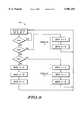
- Control circuitry 124 of FIG. 6comprises a state machine and multiplex switching circuitry having an operation outlined in FIG. 8.
- registers 126-130When CPU 12 initially begins to process address and data information, registers 126-130 will be empty. Control circuitry 124 will realize that registers 126-130 are empty and will therefore cache the first three sets of N bits of FIG. 6 into registers 126-130 as the first three sets of distinct N bits occur through address buffer 122. After registers 126-130 have been filled with valid address bits, the state machine of FIG. 8 will be implemented by control circuitry 124 resulting in an LRU replacement method on the contents of registers 126-130. In order to describe control circuitry 124 of FIG. 6, a discussion of FIG. 8 is helpful.
- FIG. 6assume that 5 banks of memory are individually capable of being enabled at any one point in time. Assume that these 5 banks of memory are referred to as bank 1 through bank 5. Further assume that the first three banks of memory accessed by CPU 12 are banks 1-3. Address bits associated with bank 1 will be stored in register 126, address bits of bank 2 will be stored in register 128, and address bits associated with bank 3 will be stored in register 130. After this initialization of controller 121, assume CPU 12 once again accesses bank 1. Since a least recently used (LRU) algorithm is employed in the state machine of FIG. 8, bank 1 must be moved to the top of registers 126-130 while maintaining the other most recently used banks 2 and 3.
- LRUleast recently used
- registers 126-130Since the order in registers 126-130 is already such that bank 1 is on top of the LRU structure formed by registers 126-130, bank 2 is in register 128 and bank 3 is in register 130, no changes need to be made to registers 126-130 due to CPU 12 accessing bank one again (i.e., registers 126-130 already contain by default the proper order of memory banks). Therefore, as illustrated in FIG. 8, when a new incoming address X equals the value stored in register A (register 126), no changes are made within registers 126-130.
- the state diagram of FIG. 8indicates that the value in register 128 is moved to register 126 while the value in register in 126 is moved down in priority to register 128 whereby the contents of register 130 are maintained as the lowest priority item in the LRU structure.
- the value in 128is the most recently used location and must be moved to the front of the queue whereby the other two remaining elements are placed near the end of the queue.
- register 126stores bank 1 as most recently used
- register 128stores bank 2
- register 130stores bank 3 as the least recently used bank.
- bank 3is accessed from CPU 12 wherein bank 3 is already stored in register 130.
- the flowchart of FIG. 8indicates that when a new address X is equal to the value C stored in register 130, that the contents of register 130 is moved to register 126 (back up into the most recently used location), the contents of register 128 are moved to register 130, and the contents of register 126 are moved to the register 128.
- This switching of contents of registersare performed by the multiplexer circuitry 124c located within control circuitry 124.
- FIG. 8indicates that the new address X which refers to bank 4 is moved into register 126 as the new most recently used item.
- Bank 1 which was in register 126is moved to register 128 and has a second priority in the queue/cache.
- the least recently used elementis now bank 2 which is moved from register 128 to register 130 in FIG. 6.
- the bank 3 which was previously stored in register 130is now removed from the entire queue and is no longer resident within the system of FIG. 6 and therefore no longer enabled by connection to VDD.
- register 126when bank 4 has been accessed, register 126 will contain bank four, register 128 will contain address bits of bank one, and register 130 will contain address bits of bank two wherein controller 121 of FIG. 6 will enable only these most recently used banks 1, 2, and 4, while banks 3 and 5 will be in a low power mode of operation.
- the registers 126-130along with the state machine implemented via control circuitry 124 and FIG. 8 allows for the three most recently used banks of memory to be identified/stored by registers 126-130.
- the comparator logic 132 of FIG. 6is utilized to determine the flow used from FIG. 8.
- the decoders 134-138 and the OR logic 140are used to send out control signals to register 24 of FIG. 1. Decoders 134-138 will each issue a one hot control signal indicating the three banks of most recently used memory which should be enabled.
- the OR logic 140will logically-OR together the three enabled signals from decoders 134-138 to result in three enable values which are then stored in register 24. Register 24 will then use these three enabled values to enable the three most recently used banks of memory within FIG. 1. All other banks of memory which are not stored within controller 121 are disabled or placed into a low powered stand by mode. This LRU/cache replacement technique and multiple entry cache avoids the thrashing previously discussed, but requires more silicon surface area in order to be implemented.
- FIG. 7illustrates an alternate controller 120.
- controller 121 and 120A primary difference between controller 121 and 120 is that the control circuitry 125 of controller operates in a manner slightly different from control circuitry 124. Instead of using shadow registers and/or multiplexer circuitry, one or more temporary storage registers 124d can be used along with address buffer 124e to perform the proper switching of contents between registers 126-130 in either a serial or parallel manner.
- the controllers of FIGS. 6 and 7are similar and provide the same functionality as previously discussed with slight changes in the state machine operation.
- FIG. 8illustrates the functional operation of the control circuitry 124 and control circuitry 125 of FIGS. 6 and 7, respectively.
- FIG. 8was previously discussed in detail with respect to FIG. 6 and a description is not repeated here for the sake of brevity.
Landscapes
- Engineering & Computer Science (AREA)
- Power Engineering (AREA)
- Theoretical Computer Science (AREA)
- Microelectronics & Electronic Packaging (AREA)
- Physics & Mathematics (AREA)
- General Engineering & Computer Science (AREA)
- General Physics & Mathematics (AREA)
- Power Sources (AREA)
- Techniques For Improving Reliability Of Storages (AREA)
- Dram (AREA)
- Memory System (AREA)
Abstract
Description
Claims (50)
Priority Applications (6)
| Application Number | Priority Date | Filing Date | Title |
|---|---|---|---|
| US08/835,363US5901103A (en) | 1997-04-07 | 1997-04-07 | Integrated circuit having standby control for memory and method thereof |
| EP98105755AEP0871178B1 (en) | 1997-04-07 | 1998-03-30 | Integrated circuit having standby control for memory |
| DE69826353TDE69826353T2 (en) | 1997-04-07 | 1998-03-30 | Integrated circuit with standby mode control circuit for memory |
| TW087104917ATW455762B (en) | 1997-04-07 | 1998-04-01 | Integrated circuit having standby control for memory |
| JP10108529AJPH10283275A (en) | 1997-04-07 | 1998-04-03 | Integrated circuit with standby control for memory |
| KR10-1998-0012195AKR100504969B1 (en) | 1997-04-07 | 1998-04-07 | Integrated circuit with standby controller for memory |
Applications Claiming Priority (1)
| Application Number | Priority Date | Filing Date | Title |
|---|---|---|---|
| US08/835,363US5901103A (en) | 1997-04-07 | 1997-04-07 | Integrated circuit having standby control for memory and method thereof |
Publications (1)
| Publication Number | Publication Date |
|---|---|
| US5901103Atrue US5901103A (en) | 1999-05-04 |
Family
ID=25269315
Family Applications (1)
| Application Number | Title | Priority Date | Filing Date |
|---|---|---|---|
| US08/835,363Expired - LifetimeUS5901103A (en) | 1997-04-07 | 1997-04-07 | Integrated circuit having standby control for memory and method thereof |
Country Status (6)
| Country | Link |
|---|---|
| US (1) | US5901103A (en) |
| EP (1) | EP0871178B1 (en) |
| JP (1) | JPH10283275A (en) |
| KR (1) | KR100504969B1 (en) |
| DE (1) | DE69826353T2 (en) |
| TW (1) | TW455762B (en) |
Cited By (36)
| Publication number | Priority date | Publication date | Assignee | Title |
|---|---|---|---|---|
| US6075731A (en)* | 1999-01-21 | 2000-06-13 | Mitsubishi Denki Kabushiki Kaisha | Memory control apparatus having data retention capabilities |
| US6079023A (en)* | 1997-12-30 | 2000-06-20 | Samsung Electronics Co., Ltd. | Multi-bank memory devices having common standby voltage generator for powering a plurality of memory array banks in response to memory array bank enable signals |
| US6151264A (en)* | 1998-11-09 | 2000-11-21 | Samsung Electronics Co., Ltd. | Integrated circuit memory devices including a single data shift block between first and second memory banks |
| WO2001001230A1 (en)* | 1999-06-29 | 2001-01-04 | Intel Corporation | Method and apparatus for dynamically changing the sizes of pools that control the power consumption levels of memory devices |
| US6175530B1 (en)* | 1999-05-14 | 2001-01-16 | Xilinx, Inc. | Method for detecting low power on an FPGA interface device |
| US6226200B1 (en)* | 1999-11-17 | 2001-05-01 | Motorola Inc. | In-circuit memory array bit cell threshold voltage distribution measurement |
| US6327664B1 (en)* | 1999-04-30 | 2001-12-04 | International Business Machines Corporation | Power management on a memory card having a signal processing element |
| US20030126413A1 (en)* | 2000-01-06 | 2003-07-03 | Tony S. El-Kik | Processor system including internal address generator for implementing single and burst data transfers |
| US20030123315A1 (en)* | 2001-12-04 | 2003-07-03 | Yasuhiko Tomohiro | Semiconductor memory device, memory system and electronic instrument |
| US6597620B1 (en)* | 2001-07-18 | 2003-07-22 | Advanced Micro Devices, Inc. | Storage circuit with data retention during power down |
| US6622198B2 (en)* | 2000-08-31 | 2003-09-16 | United Memories, Inc. | Look-ahead, wrap-around first-in, first-out integrated (FIFO) circuit device architecture |
| US20040004864A1 (en)* | 2002-07-02 | 2004-01-08 | Dell Products L.P. | On-die switchable test circuit |
| US6691235B1 (en) | 2000-07-27 | 2004-02-10 | International Business Machines Corporation | Automatic voltage regulation for processors having different voltage requirements and unified or split voltage planes |
| US20040037141A1 (en)* | 2002-08-23 | 2004-02-26 | Micron Technology, Inc. | DRAM power bus control |
| US6738305B1 (en)* | 2002-07-25 | 2004-05-18 | Taiwan Semiconductor Manufacturing Company | Standby mode circuit design for SRAM standby power reduction |
| US20040123042A1 (en)* | 2002-12-19 | 2004-06-24 | International Business Machines Corp. | Memory power management using prefetch buffers |
| US20050030819A1 (en)* | 2001-11-21 | 2005-02-10 | Jeff Koelling | Method and apparatus for standby power reduction in semiconductor devices |
| US20050052925A1 (en)* | 2003-08-28 | 2005-03-10 | Renesas Technology Corp. | Semiconductor memory device and semiconductor integrated circuit device |
| US20050166008A1 (en)* | 2004-01-22 | 2005-07-28 | Infineon Technologies Ag | Semiconductor memory device and circuit arrangement |
| US20050213416A1 (en)* | 2004-03-29 | 2005-09-29 | Nec Electronics Corporation | Semiconductor circuit apparatus with power save mode |
| US20060214738A1 (en)* | 2005-03-24 | 2006-09-28 | Wenjung Sheng | Clock circuit with programmable load capacitors |
| US20070081409A1 (en)* | 2005-09-23 | 2007-04-12 | Wuu John J | Reduced bitline leakage current |
| US20080084726A1 (en)* | 2001-10-26 | 2008-04-10 | Matsushita Electric Industrial Co., Ltd. | Semiconductor integrated circuit device and method for designing the same |
| US20080189565A1 (en)* | 2005-03-24 | 2008-08-07 | Wenjung Sheng | Automatically switching power supply sources for a clock circuit |
| US20090196115A1 (en)* | 2008-02-05 | 2009-08-06 | Renesas Technology Corp. | Semiconductor device for preventing erroneous write to memory cell in switching operational mode between normal mode and standby mode |
| US7752410B1 (en)* | 2005-01-14 | 2010-07-06 | Oracle America, Inc. | System and method for accessing data in a multicycle operations cache |
| US20100329063A1 (en)* | 2009-06-30 | 2010-12-30 | Sun Microsystems, Inc. | Dynamically controlled voltage regulator for a memory |
| US20130232365A1 (en)* | 2012-03-01 | 2013-09-05 | Semiconductor Energy Laboratory Co., Ltd. | Semiconductor device |
| US20130262903A1 (en)* | 2012-03-30 | 2013-10-03 | Balakesan Ponniah Thevar | Detecting Access to Powered Down Device |
| US8611169B2 (en) | 2011-12-09 | 2013-12-17 | International Business Machines Corporation | Fine granularity power gating |
| US8687452B2 (en)* | 2009-12-14 | 2014-04-01 | Renesas Electronics Corporation | Semiconductor memory device |
| US8909957B2 (en) | 2010-11-04 | 2014-12-09 | Lenovo Enterprise Solutions (Singapore) Pte. Ltd. | Dynamic voltage adjustment to computer system memory |
| US9183906B2 (en) | 2012-10-02 | 2015-11-10 | International Business Machines Corporation | Fine granularity power gating |
| US9189053B2 (en) | 2013-12-06 | 2015-11-17 | Freescale Semiconductor, Inc. | Performance based power management of a memory and a data storage system using the memory |
| US9786385B2 (en)* | 2015-03-02 | 2017-10-10 | Oracle International Corporation | Memory power selection using local voltage regulators |
| US10552307B2 (en)* | 2016-06-10 | 2020-02-04 | Arm Limited | Storing arrays of data in data processing systems |
Families Citing this family (7)
| Publication number | Priority date | Publication date | Assignee | Title |
|---|---|---|---|---|
| TW457485B (en)* | 1998-09-08 | 2001-10-01 | Siemens Ag | Integrated semiconductor-memory |
| DE19964018A1 (en) | 1999-12-30 | 2001-07-12 | Bosch Gmbh Robert | Arrangement for the voltage supply of a volatile semiconductor memory |
| JP4216457B2 (en)* | 2000-11-30 | 2009-01-28 | 富士通マイクロエレクトロニクス株式会社 | Semiconductor memory device and semiconductor device |
| US6917555B2 (en)* | 2003-09-30 | 2005-07-12 | Freescale Semiconductor, Inc. | Integrated circuit power management for reducing leakage current in circuit arrays and method therefor |
| DE102004047764B4 (en) | 2004-09-30 | 2006-08-10 | Infineon Technologies Ag | Memory arrangement, method for operating and using such |
| JP4354001B1 (en) | 2008-07-03 | 2009-10-28 | Necエレクトロニクス株式会社 | Memory control circuit and integrated circuit |
| JP6003420B2 (en)* | 2012-09-06 | 2016-10-05 | 富士通株式会社 | Circuit system and semiconductor device |
Citations (10)
| Publication number | Priority date | Publication date | Assignee | Title |
|---|---|---|---|---|
| US4388706A (en)* | 1980-12-01 | 1983-06-14 | General Electric Company | Memory protection arrangement |
| US4984211A (en)* | 1988-02-16 | 1991-01-08 | Texas Instruments Incorporated | Battery backup bus scheme for an ECL BiCMOS SRAM |
| US5079744A (en)* | 1989-07-13 | 1992-01-07 | Mitsubishi Denki Kabushiki Kaisha | Test apparatus for static-type semiconductor memory devices |
| US5127096A (en)* | 1988-04-20 | 1992-06-30 | Sanyo Electric Co., Ltd. | Information processor operative both in direct mapping and in bank mapping, and the method of switching the mapping schemes |
| US5283905A (en)* | 1991-06-24 | 1994-02-01 | Compaq Computer Corporation | Power supply for computer system manager |
| US5343436A (en)* | 1990-03-13 | 1994-08-30 | Canon Kabushiki Kaisha | Electronic apparatus having backup power source |
| US5537360A (en)* | 1994-09-16 | 1996-07-16 | Dallas Semiconductor Corporation | Programmable power supply systems and methods providing a write protected memory having multiple interface capability |
| US5594694A (en)* | 1995-07-28 | 1997-01-14 | Micron Quantum Devices, Inc. | Memory circuit with switch for selectively connecting an input/output pad directly to a nonvolatile memory cell |
| US5615159A (en)* | 1995-11-28 | 1997-03-25 | Micron Quantum Devices, Inc. | Memory system with non-volatile data storage unit and method of initializing same |
| US5616162A (en)* | 1990-04-11 | 1997-04-01 | Idaho Research Foundation, Inc. | Biological system for degrading nitroaromatics in water and soils |
Family Cites Families (10)
| Publication number | Priority date | Publication date | Assignee | Title |
|---|---|---|---|---|
| US3703710A (en)* | 1970-01-05 | 1972-11-21 | Hitachi Ltd | Semiconductor memory |
| EP0284276A3 (en)* | 1987-03-16 | 1990-10-03 | Donald S. Stern | Selective power gating |
| EP0426663B1 (en)* | 1988-07-28 | 1992-12-23 | Robert Bosch Gmbh | Apparatus for defined switching of a microcomputer to standby mode |
| JP3159314B2 (en)* | 1990-05-31 | 2001-04-23 | ソニー株式会社 | Semiconductor memory |
| US5251178A (en)* | 1991-03-06 | 1993-10-05 | Childers Jimmie D | Low-power integrated circuit memory |
| JP3158542B2 (en)* | 1991-10-09 | 2001-04-23 | 日本電気株式会社 | Semiconductor memory device |
| KR0136074B1 (en)* | 1992-09-11 | 1998-06-01 | 세키자와 스토무 | MOS-type SRAM with improved soft error resistance, high potential supply voltage drop detection circuit, complementary signal transition detection circuit and semiconductor device with improved internal signal time margin |
| JPH0697285A (en)* | 1992-09-16 | 1994-04-08 | Fujitsu Ltd | Semiconductor device |
| US5650973A (en)* | 1994-09-27 | 1997-07-22 | Micrel, Inc. | PCMCIA power multiplexer integrated circuit with programmable decode |
| KR0164814B1 (en)* | 1995-01-23 | 1999-02-01 | 김광호 | Voltage driving circuit of semiconductor memory device |
- 1997
- 1997-04-07USUS08/835,363patent/US5901103A/ennot_activeExpired - Lifetime
- 1998
- 1998-03-30EPEP98105755Apatent/EP0871178B1/ennot_activeExpired - Lifetime
- 1998-03-30DEDE69826353Tpatent/DE69826353T2/ennot_activeExpired - Fee Related
- 1998-04-01TWTW087104917Apatent/TW455762B/ennot_activeIP Right Cessation
- 1998-04-03JPJP10108529Apatent/JPH10283275A/enactivePending
- 1998-04-07KRKR10-1998-0012195Apatent/KR100504969B1/ennot_activeExpired - Fee Related
Patent Citations (10)
| Publication number | Priority date | Publication date | Assignee | Title |
|---|---|---|---|---|
| US4388706A (en)* | 1980-12-01 | 1983-06-14 | General Electric Company | Memory protection arrangement |
| US4984211A (en)* | 1988-02-16 | 1991-01-08 | Texas Instruments Incorporated | Battery backup bus scheme for an ECL BiCMOS SRAM |
| US5127096A (en)* | 1988-04-20 | 1992-06-30 | Sanyo Electric Co., Ltd. | Information processor operative both in direct mapping and in bank mapping, and the method of switching the mapping schemes |
| US5079744A (en)* | 1989-07-13 | 1992-01-07 | Mitsubishi Denki Kabushiki Kaisha | Test apparatus for static-type semiconductor memory devices |
| US5343436A (en)* | 1990-03-13 | 1994-08-30 | Canon Kabushiki Kaisha | Electronic apparatus having backup power source |
| US5616162A (en)* | 1990-04-11 | 1997-04-01 | Idaho Research Foundation, Inc. | Biological system for degrading nitroaromatics in water and soils |
| US5283905A (en)* | 1991-06-24 | 1994-02-01 | Compaq Computer Corporation | Power supply for computer system manager |
| US5537360A (en)* | 1994-09-16 | 1996-07-16 | Dallas Semiconductor Corporation | Programmable power supply systems and methods providing a write protected memory having multiple interface capability |
| US5594694A (en)* | 1995-07-28 | 1997-01-14 | Micron Quantum Devices, Inc. | Memory circuit with switch for selectively connecting an input/output pad directly to a nonvolatile memory cell |
| US5615159A (en)* | 1995-11-28 | 1997-03-25 | Micron Quantum Devices, Inc. | Memory system with non-volatile data storage unit and method of initializing same |
Non-Patent Citations (2)
| Title |
|---|
| Joseph M. Harris II et al., Motorola Inc., "Method and Apparatus for Testing On-Chip Memory on a Microcontroller", Application No. 08/669,863, Filed Jun. 10, 1996. |
| Joseph M. Harris II et al., Motorola Inc., Method and Apparatus for Testing On Chip Memory on a Microcontroller , Application No. 08/669,863, Filed Jun. 10, 1996.* |
Cited By (69)
| Publication number | Priority date | Publication date | Assignee | Title |
|---|---|---|---|---|
| US6079023A (en)* | 1997-12-30 | 2000-06-20 | Samsung Electronics Co., Ltd. | Multi-bank memory devices having common standby voltage generator for powering a plurality of memory array banks in response to memory array bank enable signals |
| US6151264A (en)* | 1998-11-09 | 2000-11-21 | Samsung Electronics Co., Ltd. | Integrated circuit memory devices including a single data shift block between first and second memory banks |
| US6075731A (en)* | 1999-01-21 | 2000-06-13 | Mitsubishi Denki Kabushiki Kaisha | Memory control apparatus having data retention capabilities |
| US6327664B1 (en)* | 1999-04-30 | 2001-12-04 | International Business Machines Corporation | Power management on a memory card having a signal processing element |
| US6175530B1 (en)* | 1999-05-14 | 2001-01-16 | Xilinx, Inc. | Method for detecting low power on an FPGA interface device |
| WO2001001230A1 (en)* | 1999-06-29 | 2001-01-04 | Intel Corporation | Method and apparatus for dynamically changing the sizes of pools that control the power consumption levels of memory devices |
| US6330639B1 (en) | 1999-06-29 | 2001-12-11 | Intel Corporation | Method and apparatus for dynamically changing the sizes of pools that control the power consumption levels of memory devices |
| US6226200B1 (en)* | 1999-11-17 | 2001-05-01 | Motorola Inc. | In-circuit memory array bit cell threshold voltage distribution measurement |
| US20030126413A1 (en)* | 2000-01-06 | 2003-07-03 | Tony S. El-Kik | Processor system including internal address generator for implementing single and burst data transfers |
| US6691235B1 (en) | 2000-07-27 | 2004-02-10 | International Business Machines Corporation | Automatic voltage regulation for processors having different voltage requirements and unified or split voltage planes |
| US6622198B2 (en)* | 2000-08-31 | 2003-09-16 | United Memories, Inc. | Look-ahead, wrap-around first-in, first-out integrated (FIFO) circuit device architecture |
| US6597620B1 (en)* | 2001-07-18 | 2003-07-22 | Advanced Micro Devices, Inc. | Storage circuit with data retention during power down |
| US20080084726A1 (en)* | 2001-10-26 | 2008-04-10 | Matsushita Electric Industrial Co., Ltd. | Semiconductor integrated circuit device and method for designing the same |
| US6873562B2 (en)* | 2001-11-21 | 2005-03-29 | Micrhon Technology, Inc. | Method and apparatus for standby power reduction in semiconductor devices |
| US7072230B2 (en) | 2001-11-21 | 2006-07-04 | Micron Technology, Inc. | Method and apparatus for standby power reduction in semiconductor devices |
| US20050030819A1 (en)* | 2001-11-21 | 2005-02-10 | Jeff Koelling | Method and apparatus for standby power reduction in semiconductor devices |
| US20050162943A1 (en)* | 2001-11-21 | 2005-07-28 | Jeff Koelling | Method and apparatus for standby power reduction in semiconductor devices |
| US6721231B2 (en)* | 2001-12-04 | 2004-04-13 | Seiko Epson Corporation | Semiconductor memory device, memory system and electronic instrument |
| US20030123315A1 (en)* | 2001-12-04 | 2003-07-03 | Yasuhiko Tomohiro | Semiconductor memory device, memory system and electronic instrument |
| US20040004864A1 (en)* | 2002-07-02 | 2004-01-08 | Dell Products L.P. | On-die switchable test circuit |
| US7002859B2 (en)* | 2002-07-02 | 2006-02-21 | Dell Products L.P. | On-die switchable test circuit |
| US6738305B1 (en)* | 2002-07-25 | 2004-05-18 | Taiwan Semiconductor Manufacturing Company | Standby mode circuit design for SRAM standby power reduction |
| US20050030818A1 (en)* | 2002-08-23 | 2005-02-10 | Micron Technology, Inc. | DRAM power bus control |
| US7277352B2 (en) | 2002-08-23 | 2007-10-02 | Micron Technology, Inc. | DRAM power bus control |
| US7522466B2 (en) | 2002-08-23 | 2009-04-21 | Micron Technology, Inc. | DRAM power bus control |
| US7391666B2 (en) | 2002-08-23 | 2008-06-24 | Micron Technology, Inc. | DRAM power bus control |
| US20040037141A1 (en)* | 2002-08-23 | 2004-02-26 | Micron Technology, Inc. | DRAM power bus control |
| US20080031071A1 (en)* | 2002-08-23 | 2008-02-07 | Micron Technology, Inc. | DRAM power bus control |
| US7023756B2 (en) | 2002-08-23 | 2006-04-04 | Micron Technology, Inc. | DRAM power bus control |
| US20070223301A1 (en)* | 2002-08-23 | 2007-09-27 | Micron Technology, Inc. | DRAM power bus control |
| US20060133179A1 (en)* | 2002-08-23 | 2006-06-22 | Micron Technology, Inc. | DRAM power bus control |
| US6795365B2 (en)* | 2002-08-23 | 2004-09-21 | Micron Technology, Inc. | DRAM power bus control |
| US6938146B2 (en)* | 2002-12-19 | 2005-08-30 | International Business Machines Corporation | Memory power management using prefetch buffers |
| US20040123042A1 (en)* | 2002-12-19 | 2004-06-24 | International Business Machines Corp. | Memory power management using prefetch buffers |
| US20060133180A1 (en)* | 2003-08-28 | 2006-06-22 | Renesas Technology Corp. | Semiconductor memory device and semiconductor integrated circuit device |
| US7251182B2 (en) | 2003-08-28 | 2007-07-31 | Renesas Technology Corp. | Semiconductor memory device and semiconductor integrated circuit device |
| US7031220B2 (en)* | 2003-08-28 | 2006-04-18 | Renesas Technology Corp | Semiconductor memory device and semiconductor integrated circuit device |
| US20070247952A1 (en)* | 2003-08-28 | 2007-10-25 | Noriyoshi Watanabe | Semiconductor memory device and semiconductor integrated circuit device |
| US20080247258A1 (en)* | 2003-08-28 | 2008-10-09 | Renesas Technology Corp. | Semiconductor memory device and semiconductor integrated circuit device |
| US20050052925A1 (en)* | 2003-08-28 | 2005-03-10 | Renesas Technology Corp. | Semiconductor memory device and semiconductor integrated circuit device |
| US7385870B2 (en) | 2003-08-28 | 2008-06-10 | Renesas Technology Corp. | Semiconductor memory device and semiconductor integrated circuit device |
| US7467254B2 (en)* | 2004-01-22 | 2008-12-16 | Infineon Technologies Ag | Semiconductor memory device with write protected memory banks |
| US20050166008A1 (en)* | 2004-01-22 | 2005-07-28 | Infineon Technologies Ag | Semiconductor memory device and circuit arrangement |
| US7248533B2 (en)* | 2004-03-29 | 2007-07-24 | Nec Electronics Corporation | Semiconductor circuit apparatus with power save mode |
| US20050213416A1 (en)* | 2004-03-29 | 2005-09-29 | Nec Electronics Corporation | Semiconductor circuit apparatus with power save mode |
| US7752410B1 (en)* | 2005-01-14 | 2010-07-06 | Oracle America, Inc. | System and method for accessing data in a multicycle operations cache |
| US20060214738A1 (en)* | 2005-03-24 | 2006-09-28 | Wenjung Sheng | Clock circuit with programmable load capacitors |
| US7400206B2 (en)* | 2005-03-24 | 2008-07-15 | Silicon Laboratories Inc. | Clock circuit with programmable load capacitors |
| US20080189565A1 (en)* | 2005-03-24 | 2008-08-07 | Wenjung Sheng | Automatically switching power supply sources for a clock circuit |
| US8671286B2 (en) | 2005-03-24 | 2014-03-11 | Silicon Laboratories Inc. | Automatically switching power supply sources for a clock circuit |
| US20070081409A1 (en)* | 2005-09-23 | 2007-04-12 | Wuu John J | Reduced bitline leakage current |
| US8593859B2 (en) | 2008-02-05 | 2013-11-26 | Renesas Electronics Corporation | Semiconductor device for preventing erroneous write to memory cell in switching operational mode between normal mode and standby mode |
| US20090196115A1 (en)* | 2008-02-05 | 2009-08-06 | Renesas Technology Corp. | Semiconductor device for preventing erroneous write to memory cell in switching operational mode between normal mode and standby mode |
| US7894292B2 (en)* | 2008-02-05 | 2011-02-22 | Renesas Electronics Corporation | Semiconductor device for preventing erroneous write to memory cell in switching operational mode between normal mode and standby mode |
| US20110116321A1 (en)* | 2008-02-05 | 2011-05-19 | Renesas Electronics Corporation | Semiconductor device for preventing erroneous write to memory cell in switching operational mode between normal mode and standby mode |
| US20100329063A1 (en)* | 2009-06-30 | 2010-12-30 | Sun Microsystems, Inc. | Dynamically controlled voltage regulator for a memory |
| US7924650B2 (en)* | 2009-06-30 | 2011-04-12 | Oracle America, Inc. | Dynamically controlled voltage regulator for a memory |
| US8687452B2 (en)* | 2009-12-14 | 2014-04-01 | Renesas Electronics Corporation | Semiconductor memory device |
| US8909957B2 (en) | 2010-11-04 | 2014-12-09 | Lenovo Enterprise Solutions (Singapore) Pte. Ltd. | Dynamic voltage adjustment to computer system memory |
| US8611169B2 (en) | 2011-12-09 | 2013-12-17 | International Business Machines Corporation | Fine granularity power gating |
| KR20130100719A (en)* | 2012-03-01 | 2013-09-11 | 가부시키가이샤 한도오따이 에네루기 켄큐쇼 | Semiconductor device |
| US20130232365A1 (en)* | 2012-03-01 | 2013-09-05 | Semiconductor Energy Laboratory Co., Ltd. | Semiconductor device |
| US9207751B2 (en)* | 2012-03-01 | 2015-12-08 | Semiconductor Energy Laboratory Co., Ltd. | Semiconductor device |
| US20130262903A1 (en)* | 2012-03-30 | 2013-10-03 | Balakesan Ponniah Thevar | Detecting Access to Powered Down Device |
| US9454201B2 (en)* | 2012-03-30 | 2016-09-27 | Intel Corporation | Detecting access to powered down device |
| US9183906B2 (en) | 2012-10-02 | 2015-11-10 | International Business Machines Corporation | Fine granularity power gating |
| US9189053B2 (en) | 2013-12-06 | 2015-11-17 | Freescale Semiconductor, Inc. | Performance based power management of a memory and a data storage system using the memory |
| US9786385B2 (en)* | 2015-03-02 | 2017-10-10 | Oracle International Corporation | Memory power selection using local voltage regulators |
| US10552307B2 (en)* | 2016-06-10 | 2020-02-04 | Arm Limited | Storing arrays of data in data processing systems |
Also Published As
| Publication number | Publication date |
|---|---|
| TW455762B (en) | 2001-09-21 |
| EP0871178B1 (en) | 2004-09-22 |
| EP0871178A3 (en) | 1999-12-22 |
| DE69826353D1 (en) | 2004-10-28 |
| KR100504969B1 (en) | 2005-10-24 |
| EP0871178A2 (en) | 1998-10-14 |
| DE69826353T2 (en) | 2006-02-16 |
| KR19980081140A (en) | 1998-11-25 |
| JPH10283275A (en) | 1998-10-23 |
Similar Documents
| Publication | Publication Date | Title |
|---|---|---|
| US5901103A (en) | Integrated circuit having standby control for memory and method thereof | |
| US11971773B2 (en) | Discrete power control of components within a computer system | |
| US8156357B2 (en) | Voltage-based memory size scaling in a data processing system | |
| JP3628588B2 (en) | Method for controlling power used by a memory card in a computer system | |
| JP2007109008A (en) | Semiconductor storage device, arithmetic processing unit, and storage system | |
| US11169593B2 (en) | Selective coupling of memory to voltage rails for different operating modes | |
| JP3302847B2 (en) | Storage device | |
| US7412613B2 (en) | Integrated circuit devices that support dynamic voltage scaling of power supply voltages | |
| AU736507B2 (en) | A modular cache memory battery backup system | |
| US20090089514A1 (en) | Implementing Asynchronous Request for Forcing Dynamic Memory into Self Refresh | |
| US6212609B1 (en) | Alternate access mechanism for saving and restoring state of read-only register | |
| US7209404B2 (en) | Low power memory sub-system architecture | |
| US20070094454A1 (en) | Program memory source switching for high speed and/or low power program execution in a digital processor | |
| US6549986B1 (en) | Low power instruction cache | |
| JP2005523510A (en) | Microprocessor and method for managing its power | |
| EP4111290B1 (en) | System physical address size aware cache memory | |
| KR920007908B1 (en) | The eeprom increased double in the life cycle and the control device | |
| CN116072162A (en) | Start-up protection for standby amplifier | |
| JP2012018700A (en) | Arithmetic processing unit and storage system | |
| MXPA97008606A (en) | A cache modu memory battery backup system |
Legal Events
| Date | Code | Title | Description |
|---|---|---|---|
| AS | Assignment | Owner name:MOTOROLA, INC., ILLINOIS Free format text:ASSIGNMENT OF ASSIGNORS INTEREST;ASSIGNORS:HARRIS, JOSEPH M. II;DUNN, JOHN P.;FREUND, THEO C.;AND OTHERS;REEL/FRAME:008516/0722 Effective date:19970312 | |
| STCF | Information on status: patent grant | Free format text:PATENTED CASE | |
| CC | Certificate of correction | ||
| FPAY | Fee payment | Year of fee payment:4 | |
| AS | Assignment | Owner name:FREESCALE SEMICONDUCTOR, INC., TEXAS Free format text:ASSIGNMENT OF ASSIGNORS INTEREST;ASSIGNOR:MOTOROLA, INC.;REEL/FRAME:015698/0657 Effective date:20040404 Owner name:FREESCALE SEMICONDUCTOR, INC.,TEXAS Free format text:ASSIGNMENT OF ASSIGNORS INTEREST;ASSIGNOR:MOTOROLA, INC.;REEL/FRAME:015698/0657 Effective date:20040404 | |
| FPAY | Fee payment | Year of fee payment:8 | |
| AS | Assignment | Owner name:CITIBANK, N.A. AS COLLATERAL AGENT, NEW YORK Free format text:SECURITY AGREEMENT;ASSIGNORS:FREESCALE SEMICONDUCTOR, INC.;FREESCALE ACQUISITION CORPORATION;FREESCALE ACQUISITION HOLDINGS CORP.;AND OTHERS;REEL/FRAME:018855/0129 Effective date:20061201 Owner name:CITIBANK, N.A. AS COLLATERAL AGENT,NEW YORK Free format text:SECURITY AGREEMENT;ASSIGNORS:FREESCALE SEMICONDUCTOR, INC.;FREESCALE ACQUISITION CORPORATION;FREESCALE ACQUISITION HOLDINGS CORP.;AND OTHERS;REEL/FRAME:018855/0129 Effective date:20061201 | |
| AS | Assignment | Owner name:CITIBANK, N.A., AS COLLATERAL AGENT,NEW YORK Free format text:SECURITY AGREEMENT;ASSIGNOR:FREESCALE SEMICONDUCTOR, INC.;REEL/FRAME:024397/0001 Effective date:20100413 Owner name:CITIBANK, N.A., AS COLLATERAL AGENT, NEW YORK Free format text:SECURITY AGREEMENT;ASSIGNOR:FREESCALE SEMICONDUCTOR, INC.;REEL/FRAME:024397/0001 Effective date:20100413 | |
| FPAY | Fee payment | Year of fee payment:12 | |
| AS | Assignment | Owner name:CITIBANK, N.A., AS NOTES COLLATERAL AGENT, NEW YORK Free format text:SECURITY AGREEMENT;ASSIGNOR:FREESCALE SEMICONDUCTOR, INC.;REEL/FRAME:030633/0424 Effective date:20130521 Owner name:CITIBANK, N.A., AS NOTES COLLATERAL AGENT, NEW YOR Free format text:SECURITY AGREEMENT;ASSIGNOR:FREESCALE SEMICONDUCTOR, INC.;REEL/FRAME:030633/0424 Effective date:20130521 | |
| AS | Assignment | Owner name:CITIBANK, N.A., AS NOTES COLLATERAL AGENT, NEW YORK Free format text:SECURITY AGREEMENT;ASSIGNOR:FREESCALE SEMICONDUCTOR, INC.;REEL/FRAME:031591/0266 Effective date:20131101 Owner name:CITIBANK, N.A., AS NOTES COLLATERAL AGENT, NEW YOR Free format text:SECURITY AGREEMENT;ASSIGNOR:FREESCALE SEMICONDUCTOR, INC.;REEL/FRAME:031591/0266 Effective date:20131101 | |
| AS | Assignment | Owner name:FREESCALE SEMICONDUCTOR, INC., TEXAS Free format text:PATENT RELEASE;ASSIGNOR:CITIBANK, N.A., AS COLLATERAL AGENT;REEL/FRAME:037354/0225 Effective date:20151207 Owner name:FREESCALE SEMICONDUCTOR, INC., TEXAS Free format text:PATENT RELEASE;ASSIGNOR:CITIBANK, N.A., AS COLLATERAL AGENT;REEL/FRAME:037356/0553 Effective date:20151207 Owner name:FREESCALE SEMICONDUCTOR, INC., TEXAS Free format text:PATENT RELEASE;ASSIGNOR:CITIBANK, N.A., AS COLLATERAL AGENT;REEL/FRAME:037356/0143 Effective date:20151207 | |
| AS | Assignment | Owner name:MORGAN STANLEY SENIOR FUNDING, INC., MARYLAND Free format text:ASSIGNMENT AND ASSUMPTION OF SECURITY INTEREST IN PATENTS;ASSIGNOR:CITIBANK, N.A.;REEL/FRAME:037486/0517 Effective date:20151207 | |
| AS | Assignment | Owner name:MORGAN STANLEY SENIOR FUNDING, INC., MARYLAND Free format text:ASSIGNMENT AND ASSUMPTION OF SECURITY INTEREST IN PATENTS;ASSIGNOR:CITIBANK, N.A.;REEL/FRAME:037518/0292 Effective date:20151207 | |
| AS | Assignment | Owner name:MORGAN STANLEY SENIOR FUNDING, INC., MARYLAND Free format text:SUPPLEMENT TO THE SECURITY AGREEMENT;ASSIGNOR:FREESCALE SEMICONDUCTOR, INC.;REEL/FRAME:039138/0001 Effective date:20160525 | |
| AS | Assignment | Owner name:NXP, B.V., F/K/A FREESCALE SEMICONDUCTOR, INC., NETHERLANDS Free format text:RELEASE BY SECURED PARTY;ASSIGNOR:MORGAN STANLEY SENIOR FUNDING, INC.;REEL/FRAME:040925/0001 Effective date:20160912 Owner name:NXP, B.V., F/K/A FREESCALE SEMICONDUCTOR, INC., NE Free format text:RELEASE BY SECURED PARTY;ASSIGNOR:MORGAN STANLEY SENIOR FUNDING, INC.;REEL/FRAME:040925/0001 Effective date:20160912 | |
| AS | Assignment | Owner name:NXP B.V., NETHERLANDS Free format text:RELEASE BY SECURED PARTY;ASSIGNOR:MORGAN STANLEY SENIOR FUNDING, INC.;REEL/FRAME:040928/0001 Effective date:20160622 | |
| AS | Assignment | Owner name:NXP USA, INC., TEXAS Free format text:CHANGE OF NAME;ASSIGNOR:FREESCALE SEMICONDUCTOR INC.;REEL/FRAME:040652/0180 Effective date:20161107 | |
| AS | Assignment | Owner name:NXP USA, INC., TEXAS Free format text:CORRECTIVE ASSIGNMENT TO CORRECT THE NATURE OF CONVEYANCE LISTED CHANGE OF NAME SHOULD BE MERGER AND CHANGE PREVIOUSLY RECORDED AT REEL: 040652 FRAME: 0180. ASSIGNOR(S) HEREBY CONFIRMS THE MERGER AND CHANGE OF NAME;ASSIGNOR:FREESCALE SEMICONDUCTOR INC.;REEL/FRAME:041354/0148 Effective date:20161107 | |
| AS | Assignment | Owner name:MORGAN STANLEY SENIOR FUNDING, INC., MARYLAND Free format text:CORRECTIVE ASSIGNMENT TO CORRECT THE REMOVE PATENTS 8108266 AND 8062324 AND REPLACE THEM WITH 6108266 AND 8060324 PREVIOUSLY RECORDED ON REEL 037518 FRAME 0292. ASSIGNOR(S) HEREBY CONFIRMS THE ASSIGNMENT AND ASSUMPTION OF SECURITY INTEREST IN PATENTS;ASSIGNOR:CITIBANK, N.A.;REEL/FRAME:041703/0536 Effective date:20151207 | |
| AS | Assignment | Owner name:SHENZHEN XINGUODU TECHNOLOGY CO., LTD., CHINA Free format text:CORRECTIVE ASSIGNMENT TO CORRECT THE TO CORRECT THE APPLICATION NO. FROM 13,883,290 TO 13,833,290 PREVIOUSLY RECORDED ON REEL 041703 FRAME 0536. ASSIGNOR(S) HEREBY CONFIRMS THE THE ASSIGNMENT AND ASSUMPTION OF SECURITYINTEREST IN PATENTS.;ASSIGNOR:MORGAN STANLEY SENIOR FUNDING, INC.;REEL/FRAME:048734/0001 Effective date:20190217 | |
| AS | Assignment | Owner name:NXP B.V., NETHERLANDS Free format text:RELEASE BY SECURED PARTY;ASSIGNOR:MORGAN STANLEY SENIOR FUNDING, INC.;REEL/FRAME:050744/0097 Effective date:20190903 | |
| AS | Assignment | Owner name:MORGAN STANLEY SENIOR FUNDING, INC., MARYLAND Free format text:CORRECTIVE ASSIGNMENT TO CORRECT THE REMOVE APPLICATION11759915 AND REPLACE IT WITH APPLICATION 11759935 PREVIOUSLY RECORDED ON REEL 037486 FRAME 0517. ASSIGNOR(S) HEREBY CONFIRMS THE ASSIGNMENT AND ASSUMPTION OF SECURITYINTEREST IN PATENTS;ASSIGNOR:CITIBANK, N.A.;REEL/FRAME:053547/0421 Effective date:20151207 | |
| AS | Assignment | Owner name:NXP B.V., NETHERLANDS Free format text:CORRECTIVE ASSIGNMENT TO CORRECT THE REMOVEAPPLICATION 11759915 AND REPLACE IT WITH APPLICATION11759935 PREVIOUSLY RECORDED ON REEL 040928 FRAME 0001. ASSIGNOR(S) HEREBY CONFIRMS THE RELEASE OF SECURITYINTEREST;ASSIGNOR:MORGAN STANLEY SENIOR FUNDING, INC.;REEL/FRAME:052915/0001 Effective date:20160622 | |
| AS | Assignment | Owner name:NXP, B.V. F/K/A FREESCALE SEMICONDUCTOR, INC., NETHERLANDS Free format text:CORRECTIVE ASSIGNMENT TO CORRECT THE REMOVEAPPLICATION 11759915 AND REPLACE IT WITH APPLICATION11759935 PREVIOUSLY RECORDED ON REEL 040925 FRAME 0001. ASSIGNOR(S) HEREBY CONFIRMS THE RELEASE OF SECURITYINTEREST;ASSIGNOR:MORGAN STANLEY SENIOR FUNDING, INC.;REEL/FRAME:052917/0001 Effective date:20160912 |