US5901018A - Magnetic tunnel junction magnetoresistive read head with sensing layer as rear flux guide - Google Patents
Magnetic tunnel junction magnetoresistive read head with sensing layer as rear flux guideDownload PDFInfo
- Publication number
- US5901018A US5901018AUS08/957,788US95778897AUS5901018AUS 5901018 AUS5901018 AUS 5901018AUS 95778897 AUS95778897 AUS 95778897AUS 5901018 AUS5901018 AUS 5901018A
- Authority
- US
- United States
- Prior art keywords
- layer
- ferromagnetic layer
- sensing
- head
- fixed
- Prior art date
- Legal status (The legal status is an assumption and is not a legal conclusion. Google has not performed a legal analysis and makes no representation as to the accuracy of the status listed.)
- Expired - Lifetime
Links
- 230000005291magnetic effectEffects0.000titleclaimsabstractdescription111
- 230000004907fluxEffects0.000titleabstractdescription42
- 230000005294ferromagnetic effectEffects0.000claimsabstractdescription204
- 230000004888barrier functionEffects0.000claimsabstractdescription63
- 230000005415magnetizationEffects0.000claimsabstractdescription37
- 230000005290antiferromagnetic effectEffects0.000claimsabstractdescription35
- 230000008878couplingEffects0.000claimsabstractdescription10
- 238000010168coupling processMethods0.000claimsabstractdescription10
- 238000005859coupling reactionMethods0.000claimsabstractdescription10
- 239000000463materialSubstances0.000claimsdescription25
- 239000000758substrateSubstances0.000claimsdescription21
- 230000005641tunnelingEffects0.000claimsdescription13
- 239000000696magnetic materialSubstances0.000abstractdescription7
- PNEYBMLMFCGWSK-UHFFFAOYSA-Naluminium oxideInorganic materials[O-2].[O-2].[O-2].[Al+3].[Al+3]PNEYBMLMFCGWSK-UHFFFAOYSA-N0.000description14
- 229910000640Fe alloyInorganic materials0.000description7
- 238000000151depositionMethods0.000description7
- 239000000725suspensionSubstances0.000description7
- 239000003302ferromagnetic materialSubstances0.000description6
- 229910052748manganeseInorganic materials0.000description6
- 238000000034methodMethods0.000description6
- 230000010287polarizationEffects0.000description6
- VYPSYNLAJGMNEJ-UHFFFAOYSA-NSilicium dioxideChemical compoundO=[Si]=OVYPSYNLAJGMNEJ-UHFFFAOYSA-N0.000description5
- 229910045601alloyInorganic materials0.000description5
- 239000000956alloySubstances0.000description5
- 230000008859changeEffects0.000description5
- 230000008569processEffects0.000description5
- 229910018404Al2 O3Inorganic materials0.000description4
- 229910052782aluminiumInorganic materials0.000description4
- 230000001939inductive effectEffects0.000description4
- 238000009413insulationMethods0.000description4
- 239000000203mixtureSubstances0.000description4
- 238000000992sputter etchingMethods0.000description4
- XAGFODPZIPBFFR-UHFFFAOYSA-NaluminiumChemical compound[Al]XAGFODPZIPBFFR-UHFFFAOYSA-N0.000description3
- 239000002800charge carrierSubstances0.000description3
- 230000008021depositionEffects0.000description3
- 230000006870functionEffects0.000description3
- 239000012212insulatorSubstances0.000description3
- 238000001459lithographyMethods0.000description3
- 238000004519manufacturing processMethods0.000description3
- 229910052697platinumInorganic materials0.000description3
- 230000001681protective effectEffects0.000description3
- 229910000599Cr alloyInorganic materials0.000description2
- 238000000137annealingMethods0.000description2
- 230000000903blocking effectEffects0.000description2
- 229910052681coesiteInorganic materials0.000description2
- 229910052802copperInorganic materials0.000description2
- 229910052906cristobaliteInorganic materials0.000description2
- 230000000694effectsEffects0.000description2
- 238000007737ion beam depositionMethods0.000description2
- 238000001659ion-beam spectroscopyMethods0.000description2
- 238000001755magnetron sputter depositionMethods0.000description2
- 238000000059patterningMethods0.000description2
- 238000001552radio frequency sputter depositionMethods0.000description2
- 239000000377silicon dioxideSubstances0.000description2
- 229910052682stishoviteInorganic materials0.000description2
- 239000010409thin filmSubstances0.000description2
- 229910052905tridymiteInorganic materials0.000description2
- OKTJSMMVPCPJKN-UHFFFAOYSA-NCarbonChemical compound[C]OKTJSMMVPCPJKN-UHFFFAOYSA-N0.000description1
- 229910000531Co alloyInorganic materials0.000description1
- 241001061076Melanonus zugmayeriSpecies0.000description1
- 229910001260Pt alloyInorganic materials0.000description1
- 229910000691Re alloyInorganic materials0.000description1
- 229910000929Ru alloyInorganic materials0.000description1
- 229910000612Sm alloyInorganic materials0.000description1
- 229910001362Ta alloysInorganic materials0.000description1
- 230000003321amplificationEffects0.000description1
- 239000002885antiferromagnetic materialSubstances0.000description1
- QVGXLLKOCUKJST-UHFFFAOYSA-Natomic oxygenChemical compound[O]QVGXLLKOCUKJST-UHFFFAOYSA-N0.000description1
- 229910052799carbonInorganic materials0.000description1
- 239000004020conductorSubstances0.000description1
- 238000001816coolingMethods0.000description1
- 230000003247decreasing effectEffects0.000description1
- 230000001419dependent effectEffects0.000description1
- 238000010586diagramMethods0.000description1
- 239000012777electrically insulating materialSubstances0.000description1
- 238000005516engineering processMethods0.000description1
- 239000010408filmSubstances0.000description1
- 229910052737goldInorganic materials0.000description1
- 239000007788liquidSubstances0.000description1
- 239000000314lubricantSubstances0.000description1
- 229910052751metalInorganic materials0.000description1
- 239000002184metalSubstances0.000description1
- 150000002739metalsChemical class0.000description1
- 238000003199nucleic acid amplification methodMethods0.000description1
- 230000001590oxidative effectEffects0.000description1
- 229910052760oxygenInorganic materials0.000description1
- 239000001301oxygenSubstances0.000description1
- 229910052763palladiumInorganic materials0.000description1
- 229910000889permalloyInorganic materials0.000description1
- 230000035699permeabilityEffects0.000description1
- 230000001902propagating effectEffects0.000description1
- 229910002059quaternary alloyInorganic materials0.000description1
- 230000004044responseEffects0.000description1
- 238000000926separation methodMethods0.000description1
- 239000007787solidSubstances0.000description1
- 238000004544sputter depositionMethods0.000description1
- 230000006641stabilisationEffects0.000description1
- 238000011105stabilizationMethods0.000description1
- 229910052715tantalumInorganic materials0.000description1
- 229910052721tungstenInorganic materials0.000description1
Images


Classifications
- G—PHYSICS
- G11—INFORMATION STORAGE
- G11B—INFORMATION STORAGE BASED ON RELATIVE MOVEMENT BETWEEN RECORD CARRIER AND TRANSDUCER
- G11B5/00—Recording by magnetisation or demagnetisation of a record carrier; Reproducing by magnetic means; Record carriers therefor
- G11B5/127—Structure or manufacture of heads, e.g. inductive
- G11B5/33—Structure or manufacture of flux-sensitive heads, i.e. for reproduction only; Combination of such heads with means for recording or erasing only
- G11B5/332—Structure or manufacture of flux-sensitive heads, i.e. for reproduction only; Combination of such heads with means for recording or erasing only using thin films
- G—PHYSICS
- G11—INFORMATION STORAGE
- G11B—INFORMATION STORAGE BASED ON RELATIVE MOVEMENT BETWEEN RECORD CARRIER AND TRANSDUCER
- G11B5/00—Recording by magnetisation or demagnetisation of a record carrier; Reproducing by magnetic means; Record carriers therefor
- G11B5/127—Structure or manufacture of heads, e.g. inductive
- G11B5/33—Structure or manufacture of flux-sensitive heads, i.e. for reproduction only; Combination of such heads with means for recording or erasing only
- G11B5/39—Structure or manufacture of flux-sensitive heads, i.e. for reproduction only; Combination of such heads with means for recording or erasing only using magneto-resistive devices or effects
- G11B5/3903—Structure or manufacture of flux-sensitive heads, i.e. for reproduction only; Combination of such heads with means for recording or erasing only using magneto-resistive devices or effects using magnetic thin film layers or their effects, the films being part of integrated structures
- G11B5/3906—Details related to the use of magnetic thin film layers or to their effects
- G11B5/3909—Arrangements using a magnetic tunnel junction
- G—PHYSICS
- G11—INFORMATION STORAGE
- G11B—INFORMATION STORAGE BASED ON RELATIVE MOVEMENT BETWEEN RECORD CARRIER AND TRANSDUCER
- G11B5/00—Recording by magnetisation or demagnetisation of a record carrier; Reproducing by magnetic means; Record carriers therefor
- G11B5/127—Structure or manufacture of heads, e.g. inductive
- G11B5/33—Structure or manufacture of flux-sensitive heads, i.e. for reproduction only; Combination of such heads with means for recording or erasing only
- G11B5/39—Structure or manufacture of flux-sensitive heads, i.e. for reproduction only; Combination of such heads with means for recording or erasing only using magneto-resistive devices or effects
- G11B5/3903—Structure or manufacture of flux-sensitive heads, i.e. for reproduction only; Combination of such heads with means for recording or erasing only using magneto-resistive devices or effects using magnetic thin film layers or their effects, the films being part of integrated structures
- G11B5/3906—Details related to the use of magnetic thin film layers or to their effects
- G11B5/3912—Arrangements in which the active read-out elements are transducing in association with active magnetic shields, e.g. magnetically coupled shields
Definitions
- This inventionrelates in general to magnetic tunnel junction (MTJ) devices, and more particularly to an MTJ device for use as a magnetoresistive (MR) head for reading magnetically-recorded data.
- MTJmagnetic tunnel junction
- MRmagnetoresistive
- a magnetic tunnel junction (MTJ) deviceis comprised of two ferromagnetic layers separated by a thin insulating tunnel barrier layer and is based on the phenomenon of spin-polarized electron tunneling.
- One of the ferromagnetic layershas a higher saturation field in one direction of an applied magnetic field, typically due to its higher coercivity than the other ferromagnetic layer.
- the insulating tunnel barrier layeris thin enough that quantum mechanical tunneling occurs between the ferromagnetic layers.
- the tunneling phenomenonis electron-spin dependent, making the magnetic response of the MTJ a function of the relative orientations and spin polarizations of the two ferromagnetic layers.
- the state of the MTJ memory cellis determined by measuring the resistance of the MTJ when a sense current is passed perpendicularly through the MTJ from one ferromagnetic layer to the other.
- the probability of tunneling of charge carriers across the insulating tunnel barrier layerdepends on the relative alignment of the magnetic moments (magnetization directions) of the two ferromagnetic layers.
- the tunneling currentis spin polarized, which means that the electrical current passing from one of the ferromagnetic layers, for example, a layer whose magnetic moment is fixed or prevented from rotation, is predominantly composed of electrons of one spin type (spin up or spin down, depending on the orientation of the magnetic moment of the ferromagnetic layer).
- the degree of spin polarization of the tunneling currentis determined by the electronic band structure of the magnetic material comprising the ferromagnetic layer at the interface of the ferromagnetic layer with the tunnel barrier layer.
- the first ferromagnetic layerthus acts as a spin filter.
- the probability of tunneling of the charge carriersdepends on the availability of electronic states of the same spin polarization as the spin polarization of the electrical current in the second ferromagnetic layer. Usually, when the magnetic moment of the second ferromagnetic layer is parallel to the magnetic moment of the first ferromagnetic layer, there are more available electronic states than when the magnetic moment of the second ferromagnetic layer is aligned antiparallel to that of the first ferromagnetic layer.
- the tunneling probability of the charge carriersis highest when the magnetic moments of both layers are parallel, and is lowest when the magnetic moments are antiparallel.
- the tunneling probabilitytakes an intermediate value.
- the electrical resistance of the MTJ memory celldepends on the spin polarization of the electrical current and the electronic states in both of the ferromagnetic layers.
- the two possible magnetization directions of the ferromagnetic layer whose magnetization direction is not fixeduniquely define two possible bit states (0 or 1) of the memory cell.
- a magnetoresistive (MR) sensordetects magnetic field signals through the resistance changes of a sensing element, fabricated of a magnetic material, as a function of the strength and direction of magnetic flux being sensed by the sensing element.
- Conventional MR sensorssuch as those used as MR read heads for reading data in magnetic recording disk drives, operate on the basis of the anisotropic magnetoresistive (AMR) effect of the bulk magnetic material, which is typically permalloy (Ni 81 Fe 19 ).
- a component of the read element resistancevaries as the square of the cosine of the angle between the magnetization direction in the read element and the direction of sense current through the read element.
- Recorded datacan be read from a magnetic medium, such as the disk in a disk drive, because the external magnetic field from the recorded magnetic medium (the signal field) causes a change in the direction of magnetization in the read element, which in turn causes a change in resistance of the read element and a corresponding change in the sensed current or voltage.
- the sense currentis in a direction parallel to the ferromagnetic layer of the read element.
- an MTJ deviceas a magnetoresistive read head for magnetic recording has also been proposed, as described in U.S. Pat. No. 5,390,061.
- the free and fixed ferromagnetic layershave lateral perimeters which do not extend beyond that of the lateral perimeter of the insulating tunnel barrier.
- the read headsenses flux from small magnetized regions or magnetic bits written into a thin film magnetic medium above which the head is suspended.
- Increased capacity disk drivesare achieved in part by higher magnetic bit areal densities.
- the area of each magnetic region or bitmust be decreased but this thereby gives rise to reduced magnetic flux.
- Magnetic recording headswhich can sense reduced magnetic flux with greater output signal are thereby required for higher performance and higher capacity magnetic recording disk drives.
- Improved magnetic recording read headscan be obtained by finding MTJ structures with higher magnetoresistance coefficients. However the MR coefficients are determined by the intrinsic electronic and magnetic properties of the materials comprising the MTJ.
- the inventionis an MTJ MR read head for a magnetic recording system wherein the free ferromagnetic layer also acts as a rear flux guide to direct magnetic flux from the magnetic recording medium to the tunnel junction.
- the fixed ferromagnetic layer, the tunnel barrier layer and free ferromagnetic layerall have their edges exposed at the air-bearing surface (ABS). Both the fixed and free ferromagnetic layers are in contact with opposite surfaces of the tunnel barrier layer but the free ferromagnetic layer extends beyond the back edge of either the tunnel barrier layer or the fixed ferromagnetic layer, whichever back edge is closer to the sensing surface. This assures that the magnetic flux is non-zero in the tunnel junction region.
- the magnetization direction of the fixed ferromagnetic layeris fixed in a direction generally perpendicular to the ABS and thus to the disk surface, preferably by interfacial exchange coupling with an antiferromagnetic layer.
- the magnetization direction of the free ferromagnetic layeris aligned in a direction generally parallel to the surface of the ABS in the absence of an applied magnetic field and is free to rotate in the presence of applied magnetic fields from the magnetic recording disk.
- a layer of high coercivity hard magnetic material adjacent the sides of the free ferromagnetic layerlongitudinally biases the magnetization of the free ferromagnetic layer in the preferred direction.
- the MTJ MR read headmay be formed as part of an integrated read/write head structure in which there are electrically conducting magnetic shields located on both sides of the MTJ MR read head.
- the electrical leads for sensing circuitryare formed on the two shields so that an electrical path is provided from the shields through the leads to the fixed and free ferromagnetic layers of the tunnel junction.
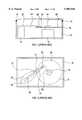
- FIG. 1is a simplified block diagram of a conventional magnetic recording disk drive for use with the recessed MTJ MR read head according to the present invention.
- FIG. 2is a top view of the disk drive of FIG. 1 with the cover removed.
- FIG. 3is a vertical cross-section of a conventional integrated inductive write head/MR read head with the MR read head located between shields and adjacent to the inductive write head for the purpose of illustrating where the MTJ MR read head of the present invention would be located.
- FIG. 4is a cross-section view taken through the tunnel junction of the MTJ MR read head of the present invention and illustrates the perpendicular direction of current flow through the tunnel junction.
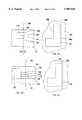
- FIG. 5is a sectional view of the rear flux guided MTJ MR read head illustrating the location of the various layers relative to sensing end of the head (the air-bearing surface).
- FIGS. 6A-6Nillustrate steps in the fabrication of the rear flux guided MTJ MR read head of the present invention.
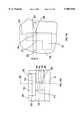
- FIG. 7is a view of the sensing surface illustrating the front edge of the MTJ device and the edges of the longitudinal biasing ferromagnetic layers.
- FIG. 1there is illustrated in sectional view a schematic of a prior art disk drive of the type using a MR sensor.
- the disk drivecomprises a base 10 to which are secured a disk drive motor 12 and an actuator 14, and a cover 11.
- the base 10 and cover 11provide a substantially sealed housing for the disk drive.
- a magnetic recording disk 16is connected to drive motor 12 by means of hub 18 to which it is attached for rotation by the drive motor 12.
- a thin lubricant film 50is maintained on the surface of disk 16.
- a read/write head or transducer 25is formed on the trailing end of a carrier, such as an air-bearing slider 20.
- Transducer 25is a read/write head comprising an inductive write head portion and a MR read head portion, as will be described with respect to FIG. 3.
- the slider 20is connected to the actuator 14 by means of a rigid arm 22 and a suspension 24.
- the suspension 24provides a biasing force which urges the slider 20 onto the surface of the recording disk 16.
- the drive motor 12rotates the disk 16 at a constant speed
- the actuator 14, which is typically a linear or rotary voice coil motor (VCM)moves the slider 20 generally radially across the surface of the disk 16 so that the read/write head 25 may access different data tracks on disk 16.
- VCMlinear or rotary voice coil motor
- FIG. 2is a top view of the interior of the disk drive with the cover 11 removed, and illustrates in better detail the suspension 24 which provides a force to the slider 20 to urge it toward the disk 16.
- the suspensionmay be a conventional type of suspension, such as the well-known Watrous suspension, as described in IBM's U.S. Pat. No. 4,167,765. This type of suspension also provides a gimbaled attachment of the slider which allows the slider to pitch and roll as it rides on the air bearing.
- the data detected from disk 16 by the transducer 25is processed into a data readback signal by signal amplification and processing circuitry in the integrated circuit chip 15 located on arm 22.
- the signals from transducer 25travel via flex cable 17 to chip 15, which sends its output signals to the disk drive electronics (not shown) via cable 19.
- FIG. 3is a cross-sectional schematic view of the integrated read/write head 25 which includes a MR read head portion and an inductive write head portion.
- the head 25is lapped to form an air-bearing surface (ABS), the ABS being spaced from the surface of the rotating disk 16 (FIG. 1) by the air bearing as discussed above.
- the read headincludes a MR sensor 40 sandwiched between first and second gap layers G1 and G2 which are, in turn, sandwiched between first and second magnetic shield layers S1 and S2.
- the MR sensor 40is an AMR sensor.
- the write headincludes a coil layer C and insulation layer I2 which are sandwiched between insulation layers I1 and I3 which are, in turn, sandwiched between first and second pole pieces P1 and P2.
- a gap layer G3is sandwiched between the first and second pole pieces P1, P2 at their pole tips adjacent to the ABS for providing a magnetic gap.
- signal currentis conducted through the coil layer C and flux is induced into the first and second pole layers P1, P2 causing flux to fringe across the pole tips at the ABS.
- This fluxmagnetizes circular tracks on the rotating disk 16 during a write operation.
- magnetized regions on the rotating disk 16inject flux into the MR sensor 40 of the read head, causing resistance changes in the MR sensor 40. These resistance changes are detected by detecting voltage changes across the MR sensor 40.
- the voltage changesare processed by the chip 15 (FIG. 2) and drive electronics and converted into user data.
- the combined head 25 shown in FIG. 3is a "merged" head in which the second shield layer S2 of the read head is employed as a first pole piece P1 for the write head. In a piggyback head (not shown), the second shield layer S2 and the first pole piece P1 are separate layers.
- Disk drivesmay contain a large number of disks and actuators, and each actuator may support a number of sliders.
- the head carriermay be one which maintains the head in contact or near contact with the disk, such as in liquid bearing and other contact and near-contact recording disk drives.
- the present inventionis a MR read head with an MTJ sensor for use in place of the MR sensor 40 in the read/write head 25 of FIG. 3.
- FIG. 4is a section view of the MTJ MR read head of the present invention as it would appear if taken through a plane whose edge is shown as line 42 in FIG. 3 and viewed from the disk surface.
- the paper of FIG. 4is a plane parallel to the ABS and through substantially the active sensing region, i.e., the tunnel junction, of the MTJ MR read head to reveal the layers that make up the head.
- the MTJ MR read headincludes an electrical lead 102 formed on the gap layer G1 substrate, an electrical lead 104 below gap layer G2, and the MTJ 100 formed as a stack of layers between electrical leads 102, 104.
- the MTJ 100includes a first electrode multilayer stack 110, an insulating tunnel barrier layer 120, and a top electrode stack 130.
- Each of the electrodesincludes a ferromagnetic layer in direct contact with tunnel barrier layer 120, i.e., ferromagnetic layers 118 and 132.
- the base electrode layer stack 110 formed on electrical lead 102includes a seed or "template” layer 112 on the lead 102, a layer of antiferromagnetic material 116 on the template layer 112, and a "fixed” ferromagnetic layer 118 formed on and exchange coupled with the underlying antiferromagnetic layer 116.
- the ferromagnetic layer 118is called the fixed layer because its magnetic moment or magnetization direction is prevented from rotation in the presence of applied magnetic fields in the desired range of interest.
- the top electrode stack 130includes a "free” or “sensing” ferromagnetic layer 132 and a protective or capping layer 134 formed on the sensing layer 132.
- the sensing ferromagnetic layer 132is not exchange coupled to an antiferromagnetic layer, and its magnetization direction is thus free to rotate in the presence of applied magnetic fields in the range of interest.
- the sensing ferromagnetic layer 132is fabricated so as to have its magnetic moment or magnetization direction (shown by arrow 133) oriented generally parallel to the ABS (the ABS is a plane parallel to the paper in FIG. 4) and generally perpendicular to the magnetization direction of the fixed ferromagnetic layer 118 in the absence of an applied magnetic field.
- the fixed ferromagnetic layer 118 in electrode stack 110 just beneath the tunnel barrier layer 120has its magnetization direction fixed by interfacial exchange coupling with the immediately underlying antiferromagnetic layer 116, which also forms part of bottom electrode stack 110.
- the magnetization direction of the fixed ferromagnetic layer 118is oriented generally perpendicular to the ABS, i.e., out of or into the paper in FIG. 4 (as shown by arrow tail 119).
- biasing ferromagnetic layer 150for longitudinally biasing the magnetization of the sensing ferromagnetic layer 132, and an insulating layer 160 separating and isolating the biasing layer 150 from the sensing ferromagnetic layer 132 and the other layers of the MTJ 100.
- the biasing ferromagnetic layer 150is a hard magnetic material, such as a CoPtCr alloy, that has its magnetic moment (shown by arrow 151) aligned in the same direction as the magnetic moment 133 of the sensing ferromagnetic layer 132 in the absence of an applied magnetic field.
- the insulating layer 160which is preferably alumina (Al 2 O 3 ) or silica (SiO 2 ), has a thickness sufficient to electrically isolate the biasing ferromagnetic layer 150 from the MTJ 100 and the electrical leads 102, 104, but is still thin enough to permit magnetostatic coupling (shown by dashed arrow 153) with the sensing ferromagnetic layer 132.
- the product M*t (where M is the magnetic moment per unit area of the material in the ferromagnetic layer and t is the thickness of the ferromagnetic layer) of the biasing ferromagnetic layer 150must be greater than or equal to the M*t of the sensing ferromagnetic layer 132 to assure stable longitudinal biasing.
- the thickness of the biasing ferromagnetic layer 150is at least approximately twice that of the sensing ferromagnetic layer 132.
- a sense current Iis directed from first electrical lead 102 perpendicularly through the antiferromagnetic layer 116, the fixed ferromagnetic layer 118, the tunnel barrier layer 120, and the sensing ferromagnetic layer 132 and then out through the second electrical lead 104.
- the amount of tunneling current through the tunnel barrier layer 120is a function of the relative orientations of the magnetizations of the fixed and sensing ferromagnetic layers 118, 132 that are adjacent to and in contact with the tunnel barrier layer 120.
- the magnetic field from the recorded datacauses the magnetization direction of sensing ferromagnetic layer 132 to rotate away from the direction 133, i.e., either into or out of the paper of FIG. 4.
- This change in resistanceis detected by the disk drive electronics and processed into data read back from the disk.
- the sense currentis prevented from reaching the biasing ferromagnetic layer 150 by the electrical insulating layer 160, which also insulates the biasing ferromagnetic layer 150 from the electrical leads 102, 104.
- a representative set of materials for MTJ 100(FIG. 4) will now be described. All of the layers of the MTJ 100 are grown in the presence of a magnetic field applied parallel to the surface of the substrate. The magnetic field serves to orient the easy axis of all of the ferromagnetic layers.
- a 5 nm Ta seed layer(not shown) is first formed on a 10-50 nm Au layer that serves as the electrical lead 102.
- the seed layeris comprised of a material which encourages the (111) growth of the face-centered cubic (fcc) Ni 81 Fe 19 template layer 112.
- the template ferromagnetic layer 112encourages the growth of the antiferromagnetic layer 116.
- Suitable seed layer materialsinclude fcc metals, such as Cu, as well as Ta or a combination of layers, such as 3-5 nm Ta/3-5 nm Cu.
- the MTJ base electrode stack 110comprises a stack of 4 nm Ni 81 Fe 19 /10 nm Fe 50 Mn 50 /8 nm Ni 81 Fe 19 (layers 112, 116, 118, respectively) grown on the Ta seed layer on the 10-20 nm Au layer 102.
- the Au lead layer 102is formed on the alumina gap material G1 that serves as the substrate.
- the tunnel barrier layer 120is formed by depositing and then plasma oxidizing a 0.5-2 nm Al layer. This creates the Al 2 O 3 insulating tunnel barrier layer 120.
- the top electrode stack 130is a 5 nm Ni--Fe/10 nm Ta stack (layers 132, 134, respectively).
- the Ta layer 134serves as a protective capping layer.
- the top electrode stack 130is contacted by a 20 nm Au layer that serves as the electrical lead 104.
- the resistance of the MTJ devicewill be largely dominated by that of the tunnel barrier layer 120.
- the resistance per unit area of the conducting leads 102, 104can be much higher than in conventional MR read heads in which the current flows parallel to the layers.
- the leads 102, 104can be made thinner and/or narrower than in conventional MR head structures, and/or can be made from intrinsically more resistive materials, such as alloys or combinations of elements.
- the layers in the bottom electrode stack 110be smooth, and that the Al 2 O 3 tunnel barrier layer 120 be free of pinholes which would electrically short the junction.
- growth by sputtering techniques known to produce good giant magnetoresistance effects in metallic multilayer stacksis sufficient.
- An alternative sensing ferromagnetic layer 132may be comprised of a thin Co or Co.sub.(100-x) Fe.sub.(x) or Ni.sub.(100-x) Fe x (x is approximately 60) layer at the interface between the sensing ferromagnetic layer 132 and the tunnel barrier layer 120, with the bulk of layer 132 being a low magnetostriction material, such as Ni.sub.(100-x) Fe x (x is approximately 19).
- An alternative fixed ferromagnetic layer 118may be comprised largely of a bulk Ni.sub.(100-x) Fe.sub.(x) layer with a thin layer of a Co or Co.sub.(100-x) Fe.sub.(x) or Ni.sub.(100-x) Fe x (x is approximately 60) layer at the interface with the tunnel barrier layer 120.
- the largest signalis obtained with Co or with the highest polarization Ni.sub.(100-x) Fe x (x is approximately 60) or Co.sub.(100-x) Fe.sub.(x) alloy (x is approximately 70).
- the interface layeris optimally about 1-2 nm thick.
- the net magnetostriction of the combined layeris arranged to be close to zero by small variations of the composition. If the bulk of layer 118 is Ni--Fe, then the composition is Ni 81 Fe 19 , the composition for which bulk Ni--Fe has zero magnetostriction.
- the Fe--Mn antiferromagnetic layer 116may be replaced with a Ni--Mn layer or other suitable antiferromagnetic layer which exchange biases the ferromagnetic material in the fixed layer 118 and which has a resistance which is substantially less than that of the Al 2 O 3 barrier layer 120.
- the fixed ferromagnetic layerhas its magnetic moment fixed by interfacial exchange coupling with an antiferromagnetic layer
- the fixed ferromagnetic layermay be formed of a magnetically "hard" high coercivity material, thereby avoiding the need for an antiferromagnetic layer.
- the MTJ device described and shown in FIG. 4has the fixed ferromagnetic layer on the bottom of MTJ 100
- the devicecan also be formed by depositing the sensing ferromagnetic layer first, followed by the tunnel barrier layer, the fixed ferromagnetic layer, and the antiferromagnetic layer. Such an MTJ device would then have the layers essentially inverted from the MTJ 100 shown in FIG. 4.
- the rear flux guided MTJ MR head of the present inventionis illustrated in a section view perpendicular to the view of FIG. 4 and with the sensing surface 200 or ABS to the right.
- the biasing ferromagnetic layer 150is not shown and in the MTJ 100 only the ferromagnetic layers, the antiferromagnetic layer and the tunnel barrier layer are shown.
- the sensing ferromagnetic layer 132has a sensing edge 202 that is substantially coplanar with the sensing surface 200 or ABS and a back edge 203.
- the fixed ferromagnetic layer 118has a front edge 206 that is substantially coplanar with the sensing surface 200 or ABS and a back edge 208.
- the antiferromagnetic layer 116has edges contiguous with the edges of the fixed ferromagnetic layer 118.
- the tunnel barrier layer 120has a front edge 210 that is also substantially coplanar with the sensing surface 200 or ABS and which is essentially coplanar with front edge 206 of the fixed ferromagnetic layer 118, and a back edge 212.
- the back edge of the sensing ferromagnetic layer 203extends beyond the back edge of either the tunnel barrier layer 212 or the fixed ferromagnetic layer 208, whichever back edge is closer to the sensing surface 200.
- the lead 102is formed on the G1 gap layer and the G2 gap layer separates the lead 104 from magnetic shield S2.
- the material of G1 and G2 and in the region behind back edges 203, 208 and 212is an electrically insulating material, preferably alumina.
- the sensing surface 200 or ABSmay have a protective overcoat formed on it, such as a thin layer of amorphous diamond-like carbon, as is known in the art to protect the head during contact with the disk.
- a MR sensorsuch as sensor 40
- the magnetic flux to be detectedenters the front edge 202 of the free ferromagnetic layer 132 at the air-bearing surface 200 and decays towards the read edge 203 of this layer.
- the fluxis constrained to be zero at the rear edge 203 of this layer.
- Some of the incident magnetic fluxleaks to the magnetic shields S1 and S2. This leakage is determined by the shield--shield gap width g, and the permeability ⁇ and thickness t of the free ferromagnetic layer 132.
- the magnetic fluxthus decays from the front edge of the free ferromagnetic layer with a characteristic length ⁇ of ( ⁇ tg/2) 0 .5.
- the fluxis constrained to be zero only at the rear edge of the rear flux guide.
- the amount of magnetic flux in the active region of the sensoris increased beyond that in the absence of such a rear flux guide. Consequently, the output signal of the MTJ sensor with the rear flux guide is enhanced by the amount of extra flux in the active region of the sensor.
- the back edges 212, 208 of the tunnel barrier layer 120 and the fixed ferromagnetic layer 118, respectively,are coplanar, they need not be so, provided the back edge 203 of the free ferromagnetic layer 132 is farther from the sensing surface 200 than whichever of back edges 212, 208 is closer to the sensing surface 200. This is because the current flow perpendicular through the tunnel barrier layer 120 is defined by whichever back edge 212, 208 is closer to the sensing surface 200.
- the back edge 203 of the sensing ferromagnetic layer 132is located farther than the back edge 212 of the tunnel barrier layer 120 if the back edge 212 is closer to the sensing surface 200 than the back edge 208 of the fixed ferromagnetic layer 118.
- the back edge 203 of the sensing ferromagnetic layer 132is located farther than the back edge 208 of the fixed ferromagnetic layer 118 if the back edge 208 is closer to the sensing surface 200 than the back edge 212 of the tunnel barrier layer 120.
- the first lead 102is shown as having its back edge extending beyond the back edges of the antiferromagnetic layer 116 and fixed ferromagnetic layer 118, the first lead 102 may have its back edge substantially coplanar with the back edges of the antiferromagnetic layer 116 and fixed ferromagnetic layer 118.
- the second lead 104is shown as having its back edge coplanar with the back edge 203 of the free ferromagnetic layer 132
- the second lead 104may have its back edge extending beyond the back edge 203 of the free ferromagnetic layer 132.
- the second lead 104may have its back edge closer to the ABS 200 than the back edge 203 of the free ferromagnetic layer 132 providing that its back edge is further from the ABS 200 than the rear edge of the active region of the sensor.
- the substrate onto which the first lead 102 is formedis the first magnetic shield S1 and the second magnetic shield S2 is formed on the second lead 104.
- the shields S1 and S2are formed of Ni--Fe alloys or Ni--Fe--Co alloys and are electrically conducting. In this embodiment an electrically conductive path is thus provided through the shield S1 to first lead 102, perpendicularly through the tunnel junction to the second lead 104 and the second shield S2.
- This embodimenteliminates the need for insulative gap layers G1, G2, although insulative material is still required at the back of the tunnel junction, as shown in FIG. 5.
- the rear flux guidecan be a continuous extension of the free ferromagnetic layer, as illustrated in the preferred embodiment in FIG. 5.
- the MTJ MR read headis fabricated on a layer of insulator, typically the alumina G1 layer, as shown in FIG. 5, but can also be fabricated directly on the bottom magnetic shield layer S1.
- the processbegins, as shown in FIG. 6A, by depositing the material for lead layer 102, an antiferromagnetic layer 116, the fixed ferromagnetic layer 118, and a material, such as aluminum, that will ultimately be oxidized to form the tunnel barrier layer 120.
- the lead materialcan be a variety of conducting materials, such as Ta, Al, Cu, Au, W and Pt with a typical thickness in the range of 100 to 500 ⁇ .
- the antiferromagnetic layer 116can be selected from a variety of well-known materials, such as Fe--Mn, Ni--Mn, Pt--Mn, Ir--Mn, Pd--Mn and Cr--Al.
- the typical thickness for the antiferromagnetic layer 116is in the range of 70 to 300 ⁇ .
- the fixed ferromagnetic layer 118is preferably a Ni--Fe alloy or a bilayer of Ni--Fe alloy and a thin film of Co. Typical thicknesses for the Ni--Fe alloy layer are 20 to 100 ⁇ and typical thicknesses for the Co layer are 2 to 20 ⁇ .
- the thickness of the aluminum for the tunnel barrier oxide layer 120is typically in the range of 5 to 20 ⁇ .
- the layersare patterned using resist 230 to define the desired shape shown in FIG. 6B, which is a top view of FIG. 6A. Ion milling then removes material not protected by resist 230, as shown in FIG. 6C.
- the lead layer 102, antiferromagnetic layer 116, fixed ferromagnetic layer 118 and tunnel barrier layerare now formed on layer G1 with the shape shown in FIG. 6D.
- the resist layer 230is typically a bilayer resist with an undercut.
- a layer of insulator 232is deposited by ion beam or RF sputtering to seal the edges of the pattern, after which the resist layer 230 is lifted off, resulting in the structure shown in FIGS. 6E-6F.
- the rear edge 208 of the fixed ferromagnetic layer 118is set as a reference point.
- the aluminum in what will become the tunnel barrier layer 120is plasma oxidized at an oxygen pressure of 100 mTorr and a power density of 25 W/cm 2 for 30-240 seconds. This forms the insulating tunnel barrier layer 120 of alumina.
- the free ferromagnetic layer 132 and the lead layer 104are deposited.
- the free ferromagnetic layer 132is typically a Ni--Fe alloy or a bilayer of Co and a Ni--Fe alloy, with a thickness from 10 to 200 ⁇ for the Ni--Fe alloy and a thickness of 2 to 20 ⁇ for the Co.
- the lead 104is formed of similar materials and thicknesses as described for the lead 102.
- the free ferromagnetic layer 132 and lead layer 104are patterned using resist 240 to define the desired shape, as shown in FIGS. 6I-6J.
- the resist layer 240is typically a bilayer resist with an undercut. Ion milling then removes material not protected by resist 240, as shown in FIGS. 6K-6L. After the ion milling step of FIG.
- An important feature defined in this second lithographic patterningis the width of the free ferromagnetic layer 132, i.e., the width w that will be exposed at the ABS.
- This stepalso defines the back edge 203 so that the free ferromagnetic layer 132 extends from the ABS and over the front edge 210 and back edge 212 of the tunnel barrier layer 120 and terminates beyond the back edge 212. As described previously, this assists in propagating flux efficiently across the entire active tunnel junction area defined by the back edges of the tunnel barrier layer 120 and fixed ferromagnetic layer 118 and the ABS 200.
- the above processcan also be adapted to provide longitudinal biasing or stabilization for the free ferromagnetic layer 132 that also serves as the flux guide, as described previously with respect to the biasing ferromagnetic layer 150 shown in FIG. 4.
- the steps shown in FIGS. 6K-Nare modified so that instead of depositing the alumina layer 242 and then lifting off the resist 240, a sequential deposition of alumina, hard biasing ferromagnetic material, and additional alumina is performed and then liftoff is done.
- FIG. 7,is a view of sensing surface 200.
- FIG. 7shows the sensing ferromagnetic layer 132 and second lead 104 with their front edges exposed at the sensing surface 200.
- the regions between the hard biasing ferromagnetic layers 150 and the sensing ferromagnetic layer 132, the first lead 102 and second lead 104are formed of insulative material, such as alumina.
- the typical alumina thicknessesare in the 100 to 500 ⁇ range and the hard biasing ferromagnetic material is usually a Co--Pt alloy with a thickness adjusted to provide 1 to 3 times the moment of the free ferromagnetic layer 132.
- the first alumina insulationcovers the edges of the sensing ferromagnetic shape and the second alumina insulation covers the top surface of the hard biasing ferromagnetic material. After the liftoff, a final patterning step is used to remove unwanted regions of hard biasing ferromagnetic material.
- the total thickness of the leads, free and fixed ferromagnetic layer, tunnel oxide layer, and antiferromagnetic layerare limited by the total separation between the shields S1 and S2. For a 5 Gbit/in 2 sensor this number ranges from 1000 to 2000 ⁇ . It is advantageous to have the free ferromagnetic layer 132 centered in this gap between the two shields. This can be accomplished by adjusting the ratio of thicknesses of the leads 104, 102.
- the MTJ MR head structureAfter the lead 104 and free ferromagnetic layer 132 have been patterned and the MTJ MR head structure is essentially complete but for the lapping step to form the ABS 200, it is still necessary to align the magnetization direction (magnetic moment) of the fixed ferromagnetic layer 118 in the proper direction. If Fe--Mn is used as the antiferromagnetic layer 116 for exchange coupling with the fixed ferromagnetic layer 118 it is antiferromagnetic as deposited. However, its magnetization must be realigned so that it can exchange couple the fixed ferromagnetic layer 118 in the proper orientation. The structure is placed in an annealing oven and the temperature is raised to approximately 180° C., which is greater than the blocking temperature of Fe--Mn.
- the Fe--Mn layerno longer gives rise to an exchange anisotropy with the fixed ferromagnetic layer 118.
- An exchange anisotropy of the ferromagnetic layer 118is developed by cooling the pair of layers 116, 118 in a magnetic field. The orientation of the magnetization of the fixed ferromagnetic layer 118 will be along the direction of the applied magnetic field. The applied magnetic field in the annealing oven thus causes the moment of the fixed ferromagnetic layer 118 to be fixed along the required direction perpendicular to the ABS, as shown by the arrow 119 in FIG. 4.
- the lead 104 and the free ferromagnetic layer 132can be formed first on the G1 substrate, with the fixed ferromagnetic layer 118, antiferromagnetic layer 116 and lead 102 being on the "top" of the MTJ during the fabrication process.
Landscapes
- Engineering & Computer Science (AREA)
- Manufacturing & Machinery (AREA)
- Magnetic Heads (AREA)
- Hall/Mr Elements (AREA)
Abstract
Description
Claims (26)
Priority Applications (8)
| Application Number | Priority Date | Filing Date | Title |
|---|---|---|---|
| US08/957,788US5901018A (en) | 1997-10-24 | 1997-10-24 | Magnetic tunnel junction magnetoresistive read head with sensing layer as rear flux guide |
| KR1019980037935AKR100295289B1 (en) | 1997-10-24 | 1998-09-15 | Magnetic tunnel junction magnetoresistive readhead with sensing layer as rear magnetic flux guide |
| MYPI98004346AMY117419A (en) | 1997-10-24 | 1998-09-22 | Magnetic tunnel junction magnetoresistive read head with sensing layer as rear flux guide |
| JP10289013AJP3004007B2 (en) | 1997-10-24 | 1998-10-12 | Magnetic tunnel junction magnetoresistive read head |
| SG9804218ASG87011A1 (en) | 1997-10-24 | 1998-10-16 | Magnetic tunnel junction magnetoresistive read head with sensing layer as rear flux guide |
| EP98308586AEP0911810B1 (en) | 1997-10-24 | 1998-10-20 | Magnetic tunnel junction devices |
| DE69835650TDE69835650T2 (en) | 1997-10-24 | 1998-10-20 | Magnetic tunnel junction devices |
| CNB981234275ACN1139916C (en) | 1997-10-24 | 1998-10-23 | Magnetic tunnel junction magnetoresistive read head with sensing layer as rear flux guide |
Applications Claiming Priority (1)
| Application Number | Priority Date | Filing Date | Title |
|---|---|---|---|
| US08/957,788US5901018A (en) | 1997-10-24 | 1997-10-24 | Magnetic tunnel junction magnetoresistive read head with sensing layer as rear flux guide |
Publications (1)
| Publication Number | Publication Date |
|---|---|
| US5901018Atrue US5901018A (en) | 1999-05-04 |
Family
ID=25500136
Family Applications (1)
| Application Number | Title | Priority Date | Filing Date |
|---|---|---|---|
| US08/957,788Expired - LifetimeUS5901018A (en) | 1997-10-24 | 1997-10-24 | Magnetic tunnel junction magnetoresistive read head with sensing layer as rear flux guide |
Country Status (8)
| Country | Link |
|---|---|
| US (1) | US5901018A (en) |
| EP (1) | EP0911810B1 (en) |
| JP (1) | JP3004007B2 (en) |
| KR (1) | KR100295289B1 (en) |
| CN (1) | CN1139916C (en) |
| DE (1) | DE69835650T2 (en) |
| MY (1) | MY117419A (en) |
| SG (1) | SG87011A1 (en) |
Cited By (63)
| Publication number | Priority date | Publication date | Assignee | Title |
|---|---|---|---|---|
| US6153062A (en)* | 1996-09-12 | 2000-11-28 | Alps Electric Co., Ltd. | Magnetoresistive sensor and head |
| US20010033464A1 (en)* | 2000-04-19 | 2001-10-25 | Tdk Corporation | Tunnel magnetoresistive effective element, a thin film magnetic head, a magnetic head device and a magnetic disk drive device |
| US6333842B1 (en)* | 1997-12-05 | 2001-12-25 | Nec Corporation | Magneto-resistance effect type composite head and production method thereof |
| US6344954B1 (en) | 1999-07-02 | 2002-02-05 | Tdk Corporation | Magneto-resistive tunnel junction head with specific flux guide structure |
| US6411478B1 (en) | 1999-02-11 | 2002-06-25 | Seagate Technology Llc | Spin tunnel junction recording heads using an edge junction structure with CIP |
| US6421212B1 (en)* | 1999-09-21 | 2002-07-16 | Read-Rite Corporation | Thin film read head structure with improved bias magnet-to-magnetoresistive element interface and method of fabrication |
| US6433970B1 (en)* | 1999-06-07 | 2002-08-13 | Read-Rite Corporation | Structure and method for redeposition free thin film CPP read sensor fabrication |
| US6462919B1 (en)* | 1999-04-28 | 2002-10-08 | Seagate Technology Llc | Spin valve sensor with exchange tabs |
| US6473275B1 (en)* | 2000-06-06 | 2002-10-29 | International Business Machines Corporation | Dual hybrid magnetic tunnel junction/giant magnetoresistive sensor |
| US6480411B1 (en)* | 1999-10-25 | 2002-11-12 | Canon Kabushiki Kaisha | Magnetoresistance effect type memory, and method and device for reproducing information from the memory |
| US6493195B1 (en)* | 1999-09-01 | 2002-12-10 | Nec Corporation | Magnetoresistance element, with lower electrode anti-erosion/flaking layer |
| US20030011946A1 (en)* | 2001-07-10 | 2003-01-16 | International Business Machines Corporation | Method and apparatus for achieving physical connection between the flux guide and the free layer and that insulates the flux guide from the shields |
| US6519124B1 (en) | 2000-03-27 | 2003-02-11 | Tdk Corporation | Magnetic tunnel junction read head using a hybrid, low-magnetization flux guide |
| US20030030948A1 (en)* | 2001-08-13 | 2003-02-13 | Eiji Umetsu | CPP type magnetic sensor or magnetic sensor using tunnel effect, and manufacturing method therefor |
| US6542343B1 (en) | 2000-08-09 | 2003-04-01 | International Business Machines Corporation | Tunnel valve head design to lower resistance |
| US6556391B1 (en)* | 1999-12-07 | 2003-04-29 | Fujitsu Limited | Biasing layers for a magnetoresistance effect magnetic head using perpendicular current flow |
| US20030086216A1 (en)* | 2001-10-25 | 2003-05-08 | Tdk Corporation | Magneto-resistive device, and magnetic head and head suspension assembly using same |
| US6567244B1 (en) | 2000-10-10 | 2003-05-20 | Hitachi Global Storage Technologies Netherlands | Differential yoke type read head |
| US6597546B2 (en)* | 2001-04-19 | 2003-07-22 | International Business Machines Corporation | Tunnel junction sensor with an antiferromagnetic (AFM) coupled flux guide |
| US20030137780A1 (en)* | 2002-01-18 | 2003-07-24 | International Business Machines Corporation | High linear density tunnel junction flux guide read head with in-stack longitudinal bias stack (LBS) |
| US6603642B1 (en) | 2000-03-15 | 2003-08-05 | Tdk Corporation | Magnetic transducer having a plurality of magnetic layers stacked alternately with a plurality of nonmagnetic layers and a fixed-orientation-of-magnetization layer and thin film magnetic head including the magnetic transducer |
| US20030178705A1 (en)* | 2002-03-25 | 2003-09-25 | International Business Machines | System and method for stabilizing a magnetic tunnel junction sensor |
| US6639763B1 (en) | 2000-03-15 | 2003-10-28 | Tdk Corporation | Magnetic transducer and thin film magnetic head |
| US6657825B2 (en) | 2001-08-02 | 2003-12-02 | International Business Machines Corporation | Self aligned magnetoresistive flux guide read head with exchange bias underneath free layer |
| US6655006B2 (en)* | 2001-06-28 | 2003-12-02 | International Business Machines Corporation | Method of making a tunnel junction sensor with a smooth interface between a pinned or free layer and a barrier layer |
| US20030223157A1 (en)* | 2002-06-03 | 2003-12-04 | Seagate Technology Llc | Side flux guide for current perpendicular to plane reader |
| US6661625B1 (en) | 2001-02-20 | 2003-12-09 | Kyusik Sin | Spin-dependent tunneling sensor with low resistance metal oxide tunnel barrier |
| US6667862B2 (en) | 2001-02-20 | 2003-12-23 | Carnegie Mellon University | Magnetoresistive read head having permanent magnet on top of magnetoresistive element |
| US6671141B2 (en) | 2000-03-17 | 2003-12-30 | Tdk Corporation | Tunnel magnetoresistive effective element, a thin film magnetic head, a magnetic head device and a magnetic disk drive device |
| US6680830B2 (en) | 2001-05-31 | 2004-01-20 | International Business Machines Corporation | Tunnel valve sensor and flux guide with improved flux transfer therebetween |
| US20040047083A1 (en)* | 2000-07-17 | 2004-03-11 | Naoya Hasegawa | Tunneling magneoresistive element and method of manufacturing the same |
| US6721147B2 (en) | 1999-12-07 | 2004-04-13 | Fujitsu Limited | Longitudinally biased magnetoresistance effect magnetic head and magnetic reproducing apparatus |
| US20040070889A1 (en)* | 2000-12-21 | 2004-04-15 | Fujitsu Limited | Magnetoresistive effect element, a magnetic head, and a magnetic reproducing apparatus therewith |
| US6738234B1 (en) | 2000-03-15 | 2004-05-18 | Tdk Corporation | Thin film magnetic head and magnetic transducer |
| US6754056B2 (en) | 2002-01-18 | 2004-06-22 | International Business Machines Corporation | Read head having a tunnel junction sensor with a free layer biased by exchange coupling with insulating antiferromagnetic (AFM) layers |
| US6757144B2 (en) | 2002-01-18 | 2004-06-29 | International Business Machines Corporation | Flux guide read head with in stack biased current perpendicular to the planes (CPP) sensor |
| US6767655B2 (en)* | 2000-08-21 | 2004-07-27 | Matsushita Electric Industrial Co., Ltd. | Magneto-resistive element |
| US20040150901A1 (en)* | 2002-11-06 | 2004-08-05 | Wayne Hiebert | Magnetic device and method of making the same |
| US6781801B2 (en) | 2001-08-10 | 2004-08-24 | Seagate Technology Llc | Tunneling magnetoresistive sensor with spin polarized current injection |
| US6795280B1 (en) | 1998-11-18 | 2004-09-21 | Seagate Technology Llc | Tunneling magneto-resistive read head with two-piece free layer |
| US20040194292A1 (en)* | 1999-07-22 | 2004-10-07 | Dionisius Van Zon Joannes Baptist Adrianus | Method of manufacturing a magnetic tunnel junction device |
| US6819530B2 (en) | 2002-09-25 | 2004-11-16 | International Business Machines Corporation | Current perpendicular to the planes (CPP) sensor with free layer stabilized by current field |
| US6833982B2 (en) | 2001-05-03 | 2004-12-21 | Hitachi Global Storage Technologies Netherlands B.V. | Magnetic tunnel junction sensor with a free layer biased by longitudinal layers interfacing top surfaces of free layer extensions which extend beyond an active region of the sensor |
| US20050135018A1 (en)* | 2002-03-28 | 2005-06-23 | Kabushiki Kaisha Toshiba | Magnetoresistance effect element having a nonmagnetic intermediate layer having a two-dimensional fluctuation of resistance |
| US20050170532A1 (en)* | 2004-01-30 | 2005-08-04 | Headway Technologies, Inc. | Novel oxidation method to fabricate low resistance TMR read head |
| US20050180061A1 (en)* | 2004-02-18 | 2005-08-18 | Hitachi Global Storage Technologies | Self-pinned read sensor design with enhanced lead stabilizing mechanism |
| SG118135A1 (en)* | 2001-05-31 | 2006-01-27 | Ibm | Tunnel valve sensor with narrow gap flux guide |
| US20060171197A1 (en)* | 2005-01-31 | 2006-08-03 | Ulrich Klostermann | Magnetoresistive memory element having a stacked structure |
| US20070063690A1 (en)* | 2003-12-23 | 2007-03-22 | Koninklijke Philips Electronic, N.V. | High sensitivity magnetic built-in current sensor |
| US20070146931A1 (en)* | 2005-12-22 | 2007-06-28 | Hitachi Global Storage Technologies | Method for fabricating a side shield for a flux guide layer for perpendicular magnetic recording |
| US20070217080A1 (en)* | 2006-03-14 | 2007-09-20 | Hitachi Global Storage Technologies | Current perpendicular to plane (CPP) magnetoresistive sensor with back flux guide |
| US20070242394A1 (en)* | 2006-04-18 | 2007-10-18 | Gill Hardayal S | Magnetoresistive (mr) element having a continuous flux guide defined by the free layer |
| US7599153B2 (en) | 2006-02-27 | 2009-10-06 | Hitachi Global Storage Technologies Netherlands B.V. | Method and apparatus providing a stabilized top shield in read head for magnetic recording |
| US20100176472A1 (en)* | 2009-01-14 | 2010-07-15 | Sony Corporation | Nonvolatile magnetic memory device |
| US20110196635A1 (en)* | 2010-02-11 | 2011-08-11 | Geeng-Jen Sheu | Contactless sensing device |
| US9306163B2 (en) | 2013-03-04 | 2016-04-05 | SK Hynix Inc. | Electronic device having resistance element |
| US9627061B2 (en) | 2013-03-04 | 2017-04-18 | SK Hynix Inc. | Electronic device having resistance element |
| US20170131368A1 (en)* | 2015-11-11 | 2017-05-11 | Analog Devices Global | Thin film resistive device for use in an integrated circuit, an integrated circuit including a thin film resistive device |
| US20190180779A1 (en)* | 2017-12-12 | 2019-06-13 | International Business Machines Corporation | Apparatus having sensors with hard spacers and low-contact-pressure head-tape interface |
| US10650846B2 (en) | 2017-12-11 | 2020-05-12 | International Business Machines Corporation | Apparatus having recessed TMR read sensor structures for robust head-tape interface |
| US10726868B2 (en) | 2017-12-12 | 2020-07-28 | International Business Machines Corporation | Apparatus having an array of write transducers having a low friction interface |
| US10748560B2 (en) | 2017-12-11 | 2020-08-18 | International Business Machines Corporation | Apparatus having low-contact-pressure head-tape interface |
| US11205447B2 (en)* | 2019-08-21 | 2021-12-21 | Headway Technologies, Inc. | Reader noise reduction using spin hall effects |
Families Citing this family (3)
| Publication number | Priority date | Publication date | Assignee | Title |
|---|---|---|---|---|
| KR100696333B1 (en)* | 1999-08-31 | 2007-03-21 | 유티스타콤코리아 유한회사 | Anti-imaging filter supports various interpolation rates in digital radio systems |
| JP2002050011A (en)* | 2000-08-03 | 2002-02-15 | Nec Corp | Magnetoresistive effect element, magnetoresistive effect head, magnetoresistive conversion system, and magnetic recording system |
| JP2008052885A (en)* | 2006-07-28 | 2008-03-06 | Fujitsu Ltd | Magnetic sensor and magnetic disk device |
Citations (7)
| Publication number | Priority date | Publication date | Assignee | Title |
|---|---|---|---|---|
| US5390061A (en)* | 1990-06-08 | 1995-02-14 | Hitachi, Ltd. | Multilayer magnetoresistance effect-type magnetic head |
| US5432734A (en)* | 1993-08-30 | 1995-07-11 | Mitsubishi Denki Kabushiki Kaisha | Magnetoresistive element and devices utilizing the same |
| US5629922A (en)* | 1995-02-22 | 1997-05-13 | Massachusetts Institute Of Technology | Electron tunneling device using ferromagnetic thin films |
| US5650958A (en)* | 1996-03-18 | 1997-07-22 | International Business Machines Corporation | Magnetic tunnel junctions with controlled magnetic response |
| US5712612A (en)* | 1996-01-02 | 1998-01-27 | Hewlett-Packard Company | Tunneling ferrimagnetic magnetoresistive sensor |
| US5729410A (en)* | 1996-11-27 | 1998-03-17 | International Business Machines Corporation | Magnetic tunnel junction device with longitudinal biasing |
| US5747859A (en)* | 1995-09-01 | 1998-05-05 | Kabushiki Kaisha Toshiba | Magnetic device and magnetic sensor using the same |
Family Cites Families (3)
| Publication number | Priority date | Publication date | Assignee | Title |
|---|---|---|---|---|
| US6219205B1 (en)* | 1995-10-10 | 2001-04-17 | Read-Rite Corporation | High density giant magnetoresistive transducer with recessed sensor |
| EP0782129A3 (en)* | 1995-12-29 | 1998-12-09 | Read-Rite Corporation | Magnetoresistive cpp mode transducer with multiple spin valve members |
| US6084752A (en)* | 1996-02-22 | 2000-07-04 | Matsushita Electric Industrial Co., Ltd. | Thin film magnetic head |
- 1997
- 1997-10-24USUS08/957,788patent/US5901018A/ennot_activeExpired - Lifetime
- 1998
- 1998-09-15KRKR1019980037935Apatent/KR100295289B1/ennot_activeExpired - Fee Related
- 1998-09-22MYMYPI98004346Apatent/MY117419A/enunknown
- 1998-10-12JPJP10289013Apatent/JP3004007B2/ennot_activeExpired - Fee Related
- 1998-10-16SGSG9804218Apatent/SG87011A1/enunknown
- 1998-10-20EPEP98308586Apatent/EP0911810B1/ennot_activeExpired - Lifetime
- 1998-10-20DEDE69835650Tpatent/DE69835650T2/ennot_activeExpired - Fee Related
- 1998-10-23CNCNB981234275Apatent/CN1139916C/ennot_activeExpired - Fee Related
Patent Citations (8)
| Publication number | Priority date | Publication date | Assignee | Title |
|---|---|---|---|---|
| US5390061A (en)* | 1990-06-08 | 1995-02-14 | Hitachi, Ltd. | Multilayer magnetoresistance effect-type magnetic head |
| US5726837A (en)* | 1990-06-08 | 1998-03-10 | Hitachi, Ltd. | Multilayer magnetoresistance effect-type magnetic head |
| US5432734A (en)* | 1993-08-30 | 1995-07-11 | Mitsubishi Denki Kabushiki Kaisha | Magnetoresistive element and devices utilizing the same |
| US5629922A (en)* | 1995-02-22 | 1997-05-13 | Massachusetts Institute Of Technology | Electron tunneling device using ferromagnetic thin films |
| US5747859A (en)* | 1995-09-01 | 1998-05-05 | Kabushiki Kaisha Toshiba | Magnetic device and magnetic sensor using the same |
| US5712612A (en)* | 1996-01-02 | 1998-01-27 | Hewlett-Packard Company | Tunneling ferrimagnetic magnetoresistive sensor |
| US5650958A (en)* | 1996-03-18 | 1997-07-22 | International Business Machines Corporation | Magnetic tunnel junctions with controlled magnetic response |
| US5729410A (en)* | 1996-11-27 | 1998-03-17 | International Business Machines Corporation | Magnetic tunnel junction device with longitudinal biasing |
Cited By (110)
| Publication number | Priority date | Publication date | Assignee | Title |
|---|---|---|---|---|
| US6352621B1 (en) | 1996-09-12 | 2002-03-05 | Alps Electric Co., Ltd. | Method of manufacturing film laminate having exchange anisotropic magnetic field |
| US6153062A (en)* | 1996-09-12 | 2000-11-28 | Alps Electric Co., Ltd. | Magnetoresistive sensor and head |
| US6333842B1 (en)* | 1997-12-05 | 2001-12-25 | Nec Corporation | Magneto-resistance effect type composite head and production method thereof |
| US6639766B2 (en) | 1997-12-05 | 2003-10-28 | Nec Corporation | Magneto-resistance effect type composite head and production method thereof |
| US6795280B1 (en) | 1998-11-18 | 2004-09-21 | Seagate Technology Llc | Tunneling magneto-resistive read head with two-piece free layer |
| US6411478B1 (en) | 1999-02-11 | 2002-06-25 | Seagate Technology Llc | Spin tunnel junction recording heads using an edge junction structure with CIP |
| US6462919B1 (en)* | 1999-04-28 | 2002-10-08 | Seagate Technology Llc | Spin valve sensor with exchange tabs |
| US7111382B1 (en) | 1999-06-07 | 2006-09-26 | Western Digital (Fremont), Inc. | Methods for fabricating redeposition free thin film CPP read sensors |
| US6833979B1 (en) | 1999-06-07 | 2004-12-21 | Western Digital (Fremont), Inc. | Structure and method for redeposition free thin film CPP read sensor fabrication |
| US6433970B1 (en)* | 1999-06-07 | 2002-08-13 | Read-Rite Corporation | Structure and method for redeposition free thin film CPP read sensor fabrication |
| US6344954B1 (en) | 1999-07-02 | 2002-02-05 | Tdk Corporation | Magneto-resistive tunnel junction head with specific flux guide structure |
| US20040194292A1 (en)* | 1999-07-22 | 2004-10-07 | Dionisius Van Zon Joannes Baptist Adrianus | Method of manufacturing a magnetic tunnel junction device |
| US6493195B1 (en)* | 1999-09-01 | 2002-12-10 | Nec Corporation | Magnetoresistance element, with lower electrode anti-erosion/flaking layer |
| US6421212B1 (en)* | 1999-09-21 | 2002-07-16 | Read-Rite Corporation | Thin film read head structure with improved bias magnet-to-magnetoresistive element interface and method of fabrication |
| US6735850B1 (en) | 1999-09-21 | 2004-05-18 | Western Digital (Fremont), Inc. | Thin film read head structure with improved bias magnet-to-magnetoresistive element interface and method of fabrication |
| US6480411B1 (en)* | 1999-10-25 | 2002-11-12 | Canon Kabushiki Kaisha | Magnetoresistance effect type memory, and method and device for reproducing information from the memory |
| US6721147B2 (en) | 1999-12-07 | 2004-04-13 | Fujitsu Limited | Longitudinally biased magnetoresistance effect magnetic head and magnetic reproducing apparatus |
| US6556391B1 (en)* | 1999-12-07 | 2003-04-29 | Fujitsu Limited | Biasing layers for a magnetoresistance effect magnetic head using perpendicular current flow |
| US6738234B1 (en) | 2000-03-15 | 2004-05-18 | Tdk Corporation | Thin film magnetic head and magnetic transducer |
| US6603642B1 (en) | 2000-03-15 | 2003-08-05 | Tdk Corporation | Magnetic transducer having a plurality of magnetic layers stacked alternately with a plurality of nonmagnetic layers and a fixed-orientation-of-magnetization layer and thin film magnetic head including the magnetic transducer |
| US6639763B1 (en) | 2000-03-15 | 2003-10-28 | Tdk Corporation | Magnetic transducer and thin film magnetic head |
| US6671141B2 (en) | 2000-03-17 | 2003-12-30 | Tdk Corporation | Tunnel magnetoresistive effective element, a thin film magnetic head, a magnetic head device and a magnetic disk drive device |
| US6519124B1 (en) | 2000-03-27 | 2003-02-11 | Tdk Corporation | Magnetic tunnel junction read head using a hybrid, low-magnetization flux guide |
| US20010033464A1 (en)* | 2000-04-19 | 2001-10-25 | Tdk Corporation | Tunnel magnetoresistive effective element, a thin film magnetic head, a magnetic head device and a magnetic disk drive device |
| US6943998B2 (en) | 2000-04-19 | 2005-09-13 | Tdk Corporation | Tunnel magnetoresistive effective element, and a thin film magnetic head, a magnetic head device and a magnetic disk drive device using same |
| US6473275B1 (en)* | 2000-06-06 | 2002-10-29 | International Business Machines Corporation | Dual hybrid magnetic tunnel junction/giant magnetoresistive sensor |
| US6751073B2 (en) | 2000-07-17 | 2004-06-15 | Alps Electric Co., Ltd. | Tunneling magnetoresistive element and method of manufacturing the same |
| US20040047083A1 (en)* | 2000-07-17 | 2004-03-11 | Naoya Hasegawa | Tunneling magneoresistive element and method of manufacturing the same |
| US7178222B2 (en) | 2000-07-17 | 2007-02-20 | Alps Electric Co., Ltd. | Method of manufacturing a tunneling magnetoresistive element |
| US6542343B1 (en) | 2000-08-09 | 2003-04-01 | International Business Machines Corporation | Tunnel valve head design to lower resistance |
| US20040213071A1 (en)* | 2000-08-21 | 2004-10-28 | Matsushita Electric Industrial Co., Ltd. | Magneto-resistive element |
| US6767655B2 (en)* | 2000-08-21 | 2004-07-27 | Matsushita Electric Industrial Co., Ltd. | Magneto-resistive element |
| US7163755B2 (en) | 2000-08-21 | 2007-01-16 | Matsushita Electric Industrial Co., Ltd. | Magneto-resistive element |
| US6567244B1 (en) | 2000-10-10 | 2003-05-20 | Hitachi Global Storage Technologies Netherlands | Differential yoke type read head |
| US7221547B2 (en)* | 2000-12-21 | 2007-05-22 | Fujitsu Limited | Magnetoresistive effect element, a magnetic head, and a magnetic reproducing apparatus therewith |
| US20040070889A1 (en)* | 2000-12-21 | 2004-04-15 | Fujitsu Limited | Magnetoresistive effect element, a magnetic head, and a magnetic reproducing apparatus therewith |
| US6667862B2 (en) | 2001-02-20 | 2003-12-23 | Carnegie Mellon University | Magnetoresistive read head having permanent magnet on top of magnetoresistive element |
| US6661625B1 (en) | 2001-02-20 | 2003-12-09 | Kyusik Sin | Spin-dependent tunneling sensor with low resistance metal oxide tunnel barrier |
| US6597546B2 (en)* | 2001-04-19 | 2003-07-22 | International Business Machines Corporation | Tunnel junction sensor with an antiferromagnetic (AFM) coupled flux guide |
| US6833982B2 (en) | 2001-05-03 | 2004-12-21 | Hitachi Global Storage Technologies Netherlands B.V. | Magnetic tunnel junction sensor with a free layer biased by longitudinal layers interfacing top surfaces of free layer extensions which extend beyond an active region of the sensor |
| US6680830B2 (en) | 2001-05-31 | 2004-01-20 | International Business Machines Corporation | Tunnel valve sensor and flux guide with improved flux transfer therebetween |
| SG118135A1 (en)* | 2001-05-31 | 2006-01-27 | Ibm | Tunnel valve sensor with narrow gap flux guide |
| US6891704B2 (en) | 2001-06-28 | 2005-05-10 | International Business Machines Corporation | Tunnel junction sensor with a smooth interface between a pinned or free layer and a barrier layer |
| US6655006B2 (en)* | 2001-06-28 | 2003-12-02 | International Business Machines Corporation | Method of making a tunnel junction sensor with a smooth interface between a pinned or free layer and a barrier layer |
| US20050064092A1 (en)* | 2001-07-10 | 2005-03-24 | Hitachi Global Storage Technologies Netherlands B.V. | Method and apparatus for achieving physical connection between the flux guide and the free layer and that insulates the flux guide from the shields |
| US7057864B2 (en) | 2001-07-10 | 2006-06-06 | Hitachi Global Storage Technologies Netherlands B.V. | Method and apparatus for achieving physical connection between the flux guide and the free layer and that insulates the flux guide from the shields |
| US20030011946A1 (en)* | 2001-07-10 | 2003-01-16 | International Business Machines Corporation | Method and apparatus for achieving physical connection between the flux guide and the free layer and that insulates the flux guide from the shields |
| US7237322B2 (en) | 2001-07-10 | 2007-07-03 | Hitachi Global Storage Technologies Netherlands B.V. | Method for making a tunnel valve head with a flux guide |
| US20040061979A1 (en)* | 2001-08-02 | 2004-04-01 | Ho Kuok San | Self aligned magnetoresistive flux guide read head with exchange bias underneath free layer |
| US7036208B2 (en) | 2001-08-02 | 2006-05-02 | Hitachi Global Storagetechnologies Netherlands B.V | Self aligned magnetoresistive flux guide read head with exchange bias underneath free layer |
| US6657825B2 (en) | 2001-08-02 | 2003-12-02 | International Business Machines Corporation | Self aligned magnetoresistive flux guide read head with exchange bias underneath free layer |
| US6781801B2 (en) | 2001-08-10 | 2004-08-24 | Seagate Technology Llc | Tunneling magnetoresistive sensor with spin polarized current injection |
| US6826022B2 (en) | 2001-08-13 | 2004-11-30 | Alps Electric Co., Ltd. | CPP type magnetic sensor or magnetic sensor using tunnel effect, and manufacturing method therefor |
| US20030030948A1 (en)* | 2001-08-13 | 2003-02-13 | Eiji Umetsu | CPP type magnetic sensor or magnetic sensor using tunnel effect, and manufacturing method therefor |
| US6992870B2 (en) | 2001-10-25 | 2006-01-31 | Tdk Corporation | Magneto-resistive device, and magnetic head and head suspension assembly using same |
| US20030086216A1 (en)* | 2001-10-25 | 2003-05-08 | Tdk Corporation | Magneto-resistive device, and magnetic head and head suspension assembly using same |
| US6888705B2 (en) | 2002-01-18 | 2005-05-03 | Hitachi Global Storage Technologies Netherlands B.V. | High linear density tunnel junction flux guide read head with in-stack longitudinal bias stack (LBS) |
| US20030137780A1 (en)* | 2002-01-18 | 2003-07-24 | International Business Machines Corporation | High linear density tunnel junction flux guide read head with in-stack longitudinal bias stack (LBS) |
| US7161773B2 (en) | 2002-01-18 | 2007-01-09 | Hitachi Global Storage Technologies Netherlands B.V. | High linear density tunnel junction flux guide read head with in-stack longitudinal bias stack (LBS) |
| US20050146812A1 (en)* | 2002-01-18 | 2005-07-07 | Hitachi Global Storage Technologies Netherlands B.V. | High linear density tunnel junction flux guide read head with in-stack longitudinal bias stack (LBS) |
| US6754056B2 (en) | 2002-01-18 | 2004-06-22 | International Business Machines Corporation | Read head having a tunnel junction sensor with a free layer biased by exchange coupling with insulating antiferromagnetic (AFM) layers |
| US6757144B2 (en) | 2002-01-18 | 2004-06-29 | International Business Machines Corporation | Flux guide read head with in stack biased current perpendicular to the planes (CPP) sensor |
| US20040196596A1 (en)* | 2002-01-18 | 2004-10-07 | Ho Kuok San | Method of making a read head having a tunnel junction sensor with a free layer biased by exchange coupling with insulating antiferromagnetic (AFM) layers |
| US6756648B2 (en) | 2002-03-25 | 2004-06-29 | International Business Machines Corporation | System and method for stabilizing a magnetic tunnel junction sensor |
| US20030178705A1 (en)* | 2002-03-25 | 2003-09-25 | International Business Machines | System and method for stabilizing a magnetic tunnel junction sensor |
| US7130164B2 (en)* | 2002-03-28 | 2006-10-31 | Kabushiki Kaisha Toshiba | Magnetoresistance effect element having a nonmagnetic intermediate layer having a two-dimensional fluctuation of resistance |
| US20050135018A1 (en)* | 2002-03-28 | 2005-06-23 | Kabushiki Kaisha Toshiba | Magnetoresistance effect element having a nonmagnetic intermediate layer having a two-dimensional fluctuation of resistance |
| US6801410B2 (en)* | 2002-06-03 | 2004-10-05 | Seagate Technology Llc | Side flux guide for current perpendicular to plane magnetoresistive transducer |
| US20030223157A1 (en)* | 2002-06-03 | 2003-12-04 | Seagate Technology Llc | Side flux guide for current perpendicular to plane reader |
| US6819530B2 (en) | 2002-09-25 | 2004-11-16 | International Business Machines Corporation | Current perpendicular to the planes (CPP) sensor with free layer stabilized by current field |
| US7682840B2 (en) | 2002-11-06 | 2010-03-23 | Imec | Magnetic device and method of making the same |
| US20060198185A1 (en)* | 2002-11-06 | 2006-09-07 | Wayne Hiebert | Magnetic device and method of making the same |
| US7068537B2 (en)* | 2002-11-06 | 2006-06-27 | Interuniversitair Microelektronica Centrum (Imec) | Magnetic device and method of making the same |
| US20040150901A1 (en)* | 2002-11-06 | 2004-08-05 | Wayne Hiebert | Magnetic device and method of making the same |
| US7619431B2 (en)* | 2003-12-23 | 2009-11-17 | Nxp B.V. | High sensitivity magnetic built-in current sensor |
| US20070063690A1 (en)* | 2003-12-23 | 2007-03-22 | Koninklijke Philips Electronic, N.V. | High sensitivity magnetic built-in current sensor |
| US7264974B2 (en) | 2004-01-30 | 2007-09-04 | Headway Technologies, Inc. | Method for fabricating a low resistance TMR read head |
| US7986497B2 (en) | 2004-01-30 | 2011-07-26 | Headway Technologies, Inc. | Low resistance TMR read head fabricated by a novel oxidation method |
| US20050170532A1 (en)* | 2004-01-30 | 2005-08-04 | Headway Technologies, Inc. | Novel oxidation method to fabricate low resistance TMR read head |
| US20070298284A1 (en)* | 2004-01-30 | 2007-12-27 | Horng Cheng T | Low resistance TMR read head fabricated by a novel oxidation method |
| US20050180061A1 (en)* | 2004-02-18 | 2005-08-18 | Hitachi Global Storage Technologies | Self-pinned read sensor design with enhanced lead stabilizing mechanism |
| US7463459B2 (en) | 2004-02-18 | 2008-12-09 | Hitachi Global Storage Technologies Netherlands B.V. | Self-pinned read sensor design with enhanced lead stabilizing mechanism |
| US20060171197A1 (en)* | 2005-01-31 | 2006-08-03 | Ulrich Klostermann | Magnetoresistive memory element having a stacked structure |
| US7515381B2 (en) | 2005-12-22 | 2009-04-07 | Hitachi Global Storage Technologies Netherlands B.V. | Method for fabricating a side shield for a flux guide layer for perpendicular magnetic recording |
| US20070146931A1 (en)* | 2005-12-22 | 2007-06-28 | Hitachi Global Storage Technologies | Method for fabricating a side shield for a flux guide layer for perpendicular magnetic recording |
| US7599153B2 (en) | 2006-02-27 | 2009-10-06 | Hitachi Global Storage Technologies Netherlands B.V. | Method and apparatus providing a stabilized top shield in read head for magnetic recording |
| US20070217080A1 (en)* | 2006-03-14 | 2007-09-20 | Hitachi Global Storage Technologies | Current perpendicular to plane (CPP) magnetoresistive sensor with back flux guide |
| US7848061B2 (en) | 2006-03-14 | 2010-12-07 | Hitachi Global Storage Technologies Netherlands B.V. | Current perpendicular to plane (CPP) magnetoresistive sensor with back flux guide |
| US20070242394A1 (en)* | 2006-04-18 | 2007-10-18 | Gill Hardayal S | Magnetoresistive (mr) element having a continuous flux guide defined by the free layer |
| US7719801B2 (en) | 2006-04-18 | 2010-05-18 | Hitachi Global Storage Technologies Netherlands, B.V. | Magnetoresistive (MR) element having a continuous flux guide defined by the free layer |
| US8659102B2 (en)* | 2009-01-14 | 2014-02-25 | Sony Corporation | Nonvolatile magnetic memory device |
| US10128432B2 (en) | 2009-01-14 | 2018-11-13 | Sony Corporation | Nonvolatile magnetic memory device |
| US10886456B2 (en) | 2009-01-14 | 2021-01-05 | Sony Corporation | Nonvolatile magnetic memory device |
| US20100176472A1 (en)* | 2009-01-14 | 2010-07-15 | Sony Corporation | Nonvolatile magnetic memory device |
| US9508919B2 (en) | 2009-01-14 | 2016-11-29 | Sony Corporation | Nonvolatile magnetic memory device |
| US20110196635A1 (en)* | 2010-02-11 | 2011-08-11 | Geeng-Jen Sheu | Contactless sensing device |
| US8532948B2 (en)* | 2010-02-11 | 2013-09-10 | Geeng-Jen Sheu | Contactless sensing device |
| US9306163B2 (en) | 2013-03-04 | 2016-04-05 | SK Hynix Inc. | Electronic device having resistance element |
| US9627061B2 (en) | 2013-03-04 | 2017-04-18 | SK Hynix Inc. | Electronic device having resistance element |
| US20170131368A1 (en)* | 2015-11-11 | 2017-05-11 | Analog Devices Global | Thin film resistive device for use in an integrated circuit, an integrated circuit including a thin film resistive device |
| US10101414B2 (en)* | 2015-11-11 | 2018-10-16 | Analog Devices Global | Thin film resistive device for use in an integrated circuit, an integrated circuit including a thin film resistive device |
| US10650846B2 (en) | 2017-12-11 | 2020-05-12 | International Business Machines Corporation | Apparatus having recessed TMR read sensor structures for robust head-tape interface |
| US10748560B2 (en) | 2017-12-11 | 2020-08-18 | International Business Machines Corporation | Apparatus having low-contact-pressure head-tape interface |
| US10726868B2 (en) | 2017-12-12 | 2020-07-28 | International Business Machines Corporation | Apparatus having an array of write transducers having a low friction interface |
| US10755732B2 (en)* | 2017-12-12 | 2020-08-25 | International Business Machines Corporation | Apparatus having sensors with hard spacers and low-contact-pressure head-tape interface |
| US20190180779A1 (en)* | 2017-12-12 | 2019-06-13 | International Business Machines Corporation | Apparatus having sensors with hard spacers and low-contact-pressure head-tape interface |
| US11205447B2 (en)* | 2019-08-21 | 2021-12-21 | Headway Technologies, Inc. | Reader noise reduction using spin hall effects |
| US11587582B2 (en) | 2019-08-21 | 2023-02-21 | Headway Technologies, Inc. | Reader noise reduction using spin hall effects |
| US11804242B2 (en) | 2019-08-21 | 2023-10-31 | Headway Technologies, Inc. | Reader noise reduction using spin hall effects |
| US12211525B2 (en) | 2019-08-21 | 2025-01-28 | Headway Technologies, Inc. | Reader noise reduction using spin hall effects |
Also Published As
| Publication number | Publication date |
|---|---|
| CN1215879A (en) | 1999-05-05 |
| JPH11213350A (en) | 1999-08-06 |
| CN1139916C (en) | 2004-02-25 |
| JP3004007B2 (en) | 2000-01-31 |
| KR19990036636A (en) | 1999-05-25 |
| DE69835650T2 (en) | 2007-09-13 |
| EP0911810A2 (en) | 1999-04-28 |
| MY117419A (en) | 2004-06-30 |
| DE69835650D1 (en) | 2006-10-05 |
| EP0911810A3 (en) | 1999-10-27 |
| EP0911810B1 (en) | 2006-08-23 |
| SG87011A1 (en) | 2002-03-19 |
| KR100295289B1 (en) | 2001-10-26 |
Similar Documents
| Publication | Publication Date | Title |
|---|---|---|
| US5901018A (en) | Magnetic tunnel junction magnetoresistive read head with sensing layer as rear flux guide | |
| US5898547A (en) | Magnetic tunnel junction magnetoresistive read head with sensing layer as flux guide | |
| US5898548A (en) | Shielded magnetic tunnel junction magnetoresistive read head | |
| US5729410A (en) | Magnetic tunnel junction device with longitudinal biasing | |
| US6023395A (en) | Magnetic tunnel junction magnetoresistive sensor with in-stack biasing | |
| US6005753A (en) | Magnetic tunnel junction magnetoresistive read head with longitudinal and transverse bias | |
| US5966012A (en) | Magnetic tunnel junction device with improved fixed and free ferromagnetic layers | |
| US6223420B1 (en) | Method of making a read head with high resistance soft magnetic flux guide layer for enhancing read sensor efficiency | |
| US6473275B1 (en) | Dual hybrid magnetic tunnel junction/giant magnetoresistive sensor | |
| US6097579A (en) | Tunnel junction head structure without current shunting | |
| US6985338B2 (en) | Insulative in-stack hard bias for GMR sensor stabilization | |
| US20020167767A1 (en) | Magnetic tunnel junction sensor with non-shunting stabilization | |
| JP4191574B2 (en) | Magnetoresistive sensor with anti-parallel coupled wire / sensor overlap region | |
| US7237322B2 (en) | Method for making a tunnel valve head with a flux guide | |
| KR100502752B1 (en) | Magneto-resistive element, magneto-resistive head, and magnetic recording/reproducing apparatus | |
| US7133264B2 (en) | High resistance sense current perpendicular-to-plane (CPP) giant magnetoresistive (GMR) head | |
| JP3618601B2 (en) | Magnetoresistive head and magnetic reproducing apparatus |
Legal Events
| Date | Code | Title | Description |
|---|---|---|---|
| AS | Assignment | Owner name:INTERNATIONAL BUSINESS MACHINES CORPORATION, NEW Y Free format text:ASSIGNMENT OF ASSIGNORS INTEREST;ASSIGNORS:FONTANA, ROBERT E., JR.;PARKIN, STUART S. P.;TSANG, CHING H.;AND OTHERS;REEL/FRAME:008796/0928 Effective date:19971024 | |
| STCF | Information on status: patent grant | Free format text:PATENTED CASE | |
| FEPP | Fee payment procedure | Free format text:PAYOR NUMBER ASSIGNED (ORIGINAL EVENT CODE: ASPN); ENTITY STATUS OF PATENT OWNER: LARGE ENTITY | |
| FPAY | Fee payment | Year of fee payment:4 | |
| AS | Assignment | Owner name:MARIANA HDD B.V., NETHERLANDS Free format text:ASSIGNMENT OF ASSIGNORS INTEREST;ASSIGNOR:INTERNATIONAL BUSINESS MACHINES CORPORATION;REEL/FRAME:013663/0348 Effective date:20021231 | |
| AS | Assignment | Owner name:HITACHI GLOBAL STORAGE TECHNOLOGIES NETHERLANDS B. Free format text:CHANGE OF NAME;ASSIGNOR:MARIANA HDD B.V.;REEL/FRAME:013746/0146 Effective date:20021231 | |
| FEPP | Fee payment procedure | Free format text:PAYOR NUMBER ASSIGNED (ORIGINAL EVENT CODE: ASPN); ENTITY STATUS OF PATENT OWNER: LARGE ENTITY Free format text:PAYER NUMBER DE-ASSIGNED (ORIGINAL EVENT CODE: RMPN); ENTITY STATUS OF PATENT OWNER: LARGE ENTITY | |
| FPAY | Fee payment | Year of fee payment:8 | |
| FPAY | Fee payment | Year of fee payment:12 | |
| AS | Assignment | Owner name:HGST, NETHERLANDS B.V., NETHERLANDS Free format text:CHANGE OF NAME;ASSIGNOR:HGST, NETHERLANDS B.V.;REEL/FRAME:029341/0777 Effective date:20120723 Owner name:HGST NETHERLANDS B.V., NETHERLANDS Free format text:CHANGE OF NAME;ASSIGNOR:HITACHI GLOBAL STORAGE TECHNOLOGIES NETHERLANDS B.V.;REEL/FRAME:029341/0777 Effective date:20120723 | |
| AS | Assignment | Owner name:WESTERN DIGITAL TECHNOLOGIES, INC., CALIFORNIA Free format text:ASSIGNMENT OF ASSIGNORS INTEREST;ASSIGNOR:HGST NETHERLANDS B.V.;REEL/FRAME:040818/0551 Effective date:20160831 |