US5900340A - One dimensional lithographic proximity correction using DRC shape functions - Google Patents
One dimensional lithographic proximity correction using DRC shape functionsDownload PDFInfo
- Publication number
- US5900340A US5900340AUS08/805,863US80586397AUS5900340AUS 5900340 AUS5900340 AUS 5900340AUS 80586397 AUS80586397 AUS 80586397AUS 5900340 AUS5900340 AUS 5900340A
- Authority
- US
- United States
- Prior art keywords
- shape
- shapes
- edge
- design
- grown
- Prior art date
- Legal status (The legal status is an assumption and is not a legal conclusion. Google has not performed a legal analysis and makes no representation as to the accuracy of the status listed.)
- Expired - Lifetime
Links
Images


Classifications
- G—PHYSICS
- G03—PHOTOGRAPHY; CINEMATOGRAPHY; ANALOGOUS TECHNIQUES USING WAVES OTHER THAN OPTICAL WAVES; ELECTROGRAPHY; HOLOGRAPHY
- G03F—PHOTOMECHANICAL PRODUCTION OF TEXTURED OR PATTERNED SURFACES, e.g. FOR PRINTING, FOR PROCESSING OF SEMICONDUCTOR DEVICES; MATERIALS THEREFOR; ORIGINALS THEREFOR; APPARATUS SPECIALLY ADAPTED THEREFOR
- G03F7/00—Photomechanical, e.g. photolithographic, production of textured or patterned surfaces, e.g. printing surfaces; Materials therefor, e.g. comprising photoresists; Apparatus specially adapted therefor
- G03F7/70—Microphotolithographic exposure; Apparatus therefor
- G03F7/70425—Imaging strategies, e.g. for increasing throughput or resolution, printing product fields larger than the image field or compensating lithography- or non-lithography errors, e.g. proximity correction, mix-and-match, stitching or double patterning
- G03F7/70433—Layout for increasing efficiency or for compensating imaging errors, e.g. layout of exposure fields for reducing focus errors; Use of mask features for increasing efficiency or for compensating imaging errors
- G03F7/70441—Optical proximity correction [OPC]
- G—PHYSICS
- G03—PHOTOGRAPHY; CINEMATOGRAPHY; ANALOGOUS TECHNIQUES USING WAVES OTHER THAN OPTICAL WAVES; ELECTROGRAPHY; HOLOGRAPHY
- G03F—PHOTOMECHANICAL PRODUCTION OF TEXTURED OR PATTERNED SURFACES, e.g. FOR PRINTING, FOR PROCESSING OF SEMICONDUCTOR DEVICES; MATERIALS THEREFOR; ORIGINALS THEREFOR; APPARATUS SPECIALLY ADAPTED THEREFOR
- G03F1/00—Originals for photomechanical production of textured or patterned surfaces, e.g., masks, photo-masks, reticles; Mask blanks or pellicles therefor; Containers specially adapted therefor; Preparation thereof
- G03F1/36—Masks having proximity correction features; Preparation thereof, e.g. optical proximity correction [OPC] design processes
Definitions
- the present inventiongenerally relates to Very Large Scale Integrated (VLSI) lithography mask design, and more specifically to one dimensional proximity correction of VLSI design databases using Design Rule Checking (DRC) shape functions.
- VLSIVery Large Scale Integrated
- DRCDesign Rule Checking
- the invention hereindiscloses algorithms for applying Lithographic Proximity Correction (LPC) to very large scale integrated (VLSI) circuit design databases to compensate for 1-dimensional (1-D) photolithographic errors.
- LPCLithographic Proximity Correction
- Lithographic proximity correctionis used in very large scale integrated circuits to correct for printing errors such as one-dimensional lithographic errors.
- one-dimensional lithographic printing errorsmay occur because of electromagnetic diffraction from parallel edges of a mask feature during the lithographic printing process.
- densely placed parallel transistor gatescan be affected by this diffraction phenomenon differently from isolated transistor gates.
- reticle, photoresist diffusion, and etch effectscan cause 1-D lithographic printing errors.
- LPCis used to correct for these optical and non-optical undesirable printing errors, by adding or subtracting other features or shapes to or from the original design shape. The other features are used to modify the original design in order to compensate for certain undesirable effects that may take place during printing.
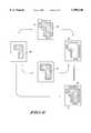
- FIG. 1 and FIG. 2together are used to illustrate a one-dimensional proximity effect.
- FIG. 1illustrates original shapes 10, 11 and 12.
- Shapes 10, 11 and 12are original design shapes positioned adjacent to each other, and separated by a certain minimum spacing.
- FIG. 2illustrates original shapes 10, 11 and 12 as they would appear 10', 11' and 12' after printing due to one-dimensional lithographic proximity effects.
- the portion of shape 11' which is not located near another shapetends to be larger than that portion of 11' which is positioned between shapes 10' and 12'.
- These types of one-dimensional proximity effectsadversely affect the effective gate length in an integrated circuit where shapes 10', 11' and 12' are formed from a polysilicon layer on top of a semiconductor substrate 13, and are used to create transistor gates.
- FIG. 3 and FIG. 4together illustrate features which may be used to correct or compensate for the one-dimensional proximity effects illustrated by FIG. 1 and FIG. 2.
- FIG. 3illustrates the positioning of edge biases 14, 15, 16 and 17 with the edges of original shapes 10, 11 and 12 to increase the effective width of original shapes 10, 11 and 12 beyond the original designed dimensions in order to print at their original design dimensions. So, unlike the shape 11' illustrated in FIG. 2, shape 11 illustrated in FIG. 3 will have a uniform width throughout its length.
- FIG. 4.illustrates assist features for correcting one-dimensional proximity effects.
- a uniform width of shape 11is provided by using subresolution assist features 19 and 20 to simulate an area of high density shapes without actually printing additional shapes. Assist features 19 and 20 are intentionally too narrow to print because they are substantially narrower than the resolution limit of a lithographic process.
- Edge biasing featuresare generally used in areas where there are many closely spaced shapes.
- assist featuresare generally used in isolated areas.
- FIG. 1 and FIG. 2 togetherare used to illustrate a one-dimensional proximity effect
- FIG. 3 and FIG. 4together illustrate features which may be used to correct or compensate for the one-dimensional proximity effects illustrated by FIG. 1 and FIG. 2;
- FIG. 5 and FIG. 6together illustrate a method for creating assist features in accordance with one embodiment of the present invention
- FIG. 7 and FIG. 8together illustrate a method for generating assist features in accordance with a second embodiment of the present invention
- FIG. 9 and FIG. 10together illustrate a method for generating edge biasing shapes in accordance with one embodiment of the present invention
- FIG. 11 and FIG. 12together illustrate a method for generating edge bias shapes in accordance with another embodiment of the present invention.
- FIG. 13is a block diagram that illustrates integrated circuit fabrication utilizing the LPC techniques disclosed herein.
- FIG. 14is a block diagram showing a General Purpose Computer.
- the present inventionprovides a method for correcting certain lithographic printing errors in very large scale integrated circuits (VLSI).
- VLSIvery large scale integrated circuits
- the methodis implemented as software and operates on a physical design database.
- a physical design databasespecifies the geometries of electronic devices used as circuit elements in an integrated circuit, such as transistors, resistors, capacitors, etc.
- the present inventionincludes algorithms that are described using operations similar to the high-level scripting languages used by existing Design Rule Checking (DRC) software.
- DRC software applicationshave been around for many years, and are not only stable and robust, but also very similar.
- DRC softwarehas the capability of generating shapes according to user specified rules. This capability is used to support the verification of layout design rules. In DRC applications such shapes are used as an intermediate step and are not intended to be printed or merged with the design database.
- LPCuses the same shape generating capability, but leaves the shapes in the database.
- the rules for generating the LPC shapesi.e., the algorithms of this invention are written so that the resulting shapes will account for the lithographic transformations that will take place during printing.
- the present inventionprovides a method for adding assist features to a semiconductor design to form an altered semiconductor design.
- the methodcomprises the steps of: performing a growing function on a base shape by a first amount to produce a first shape; performing the growing function on the base shape by a second amount to produce a second shape; subtracting the second shape from the first shape to produce a third shape; and unioning the base shape and the third shape to form a final shape.
- the growing functionmay an edge-out function that moves each edge of the base shape outward a fixed amount in a direction such that it remains parallel to each original edge of the base shape.
- the growing functionmay be an expansion function that moves vertices of the base shape outward a fixed amount along all lines bisecting each original vertice of the base shape.
- a lithographic reticlemay be produced utilizing the method above by forming reflecting or opaquing bodies on the lithographic reticle corresponding to the altered semiconductor design.
- the lithographic reticle corresponding to the altered semiconductor designmay be used to create a pattern on a semiconductor device.
- Integrated circuitsmay be fabricated utilizing the above method by generating an altered semiconductor design file containing the final shape; creating a set of one or more lithographic masks from the altered semiconductor design file; and fabricating a plurality of integrated circuits from the set of one or more lithographic masks.
- a method of applying edge biasing correction to a semiconductor design to compensate for proximity effects to form an altered semiconductor designcomprises the steps of: defining a maximum distance separating a plurality of original design shapes for applying an edge biasing correction; producing a space shape comprising a space between the plurality of original design shapes that falls below a maximum separating distance; performing a grow function on the plurality of original design shapes by a predetermined amount to produce an oversize shape; intersecting the space shape with the oversize shape to produce a biasing shape; and unioning the plurality of original design shapes with the biasing shape to form a final shape.
- the above step of producing a space shapealso comprises the substeps of: growing the plurality of original design shapes by half of the maximum separating distance to form a first grown shape; shrinking the first grown shape by half of the maximum separating distance to form a second grown shape; and subtracting the plurality of original design shapes from the second grown shape to form the space shape.
- a lithographic reticlecan be used to implement this method by forming reflecting or opaquing bodies on the lithographic reticle corresponding to the altered semiconductor design to create a pattern on a semiconductor device.
- a design filemay be generated for fabricating an integrated circuit using an altered semiconductor design file containing the final shape.
- a set of one or more lithographic masks from the altered semiconductor design filemay be created.
- a plurality of integrated circuits from the set of one or more lithographic masksmay be fabricated.
- a method of applying edge biasing correction to a semiconductor design to compensate for proximity effects to form an altered semiconductor designcomprises the steps of: defining a maximum distance separating a plurality of base shapes for applying the edge biasing correction; producing a space shape comprising a space between the plurality of base shapes that falls below a maximum separating distance; growing each edge of the space shape by a predetermined amount to create a grown space shape; intersecting the plurality of base shapes with the grown space shape to create an edge shape; growing each edge of the edge shape by a predetermined amount to create a grown edge shape; intersecting the space shape with the grown edge shape to provide a bias shape; and unioning the bias shape with the plurality of base shapes to form a final shape.
- the step of producing the space shapemay comprise the substeps of: growing the plurality of original design shapes by half of the maximum separating distance to form a first grown shape; shrinking the first grown shape by half of the maximum separating distance to form a second grown shape; and subtracting the plurality of original design shapes from the second grown shape to form the space shape.
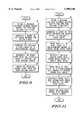
- FIG. 5is a flow chart that illustrates a method for creating assist features in accordance with one embodiment of the present invention.
- FIG. 6is a portion of a circuit layout that illustrates the method for creating assist features illustrated in FIG. 5.
- base shape 32is formed on a semiconductor substrate in polysilicon.
- base shape 32may be formed in other materials, such as metal.
- the edges of base shape 32are extended out by a predetermined amount to create an edge-expanded shape 34. Edge-expanded shape 34 is created by moving each edge of base shape 32 away from the interior of shape 32 without changing the length of the sides.
- step 26where the sides of shape 32 are edge-expanded by a second amount, to create an edge expanded shape 36, where the second amount is less than the amount in step 24.
- step 28the shape created in step 26 is subtracted from the shape created in step 24, resulting in the creation of assist features 38.
- step 30the union of assist features 38 with base shape 32 provide a final shape used for printing. As noted above, assist features 38 are narrower for the wave length of exposure used, and will not appear in the final printed circuit.
- FIG. 7is a flow chart that illustrates a method for generating assist features in accordance with a second embodiment of the present invention.
- FIG. 8is a portion of a circuit layout that illustrates the method of FIG. 7.
- an original or base shape 32is provided in which assist features are to be generated.
- the size of base shape 32is expanded by a first predetermined amount to provide a expanded shape 50.
- base shape 32is expanded by a second amount to provide a second expanded shape 52 (illustrated in FIG. 8), and expanded shape 52 is smaller than expanded shape 50 in FIG. 8.
- expanded shape 52is subtracted from expanded shape 50 to provide a continuous assist feature 54 around base shape 48.
- a union of base shape 32 with assist feature 54provides a final shape for printing.
- the width of assist feature 54is less than the resolution limit and only base shape 32 will be printed.
- FIG. 9is a flow chart that illustrates a method for generating edge biasing shapes in accordance with one embodiment of the present invention.
- FIG. 10is a portion of a circuit layout that illustrates the method illustrated in FIG. 9. Referring to both FIG. 9 and FIG. 10, starting at step 50, a predetermined distance between shapes is chosen for selecting which features edge biasing correction is to be applied. For adjacent features separated by less than the predetermined amount, such as features 60 and 62 in FIG. 10, a shape of space between original features 60 and 62 is generated as illustrated in step 52. FIG. 10 illustrates one method for generating a shape of the space 68 between original features 60 and 62. Referring to FIG.
- original design shapes 60 and 62are oversized by one-half of the distance between adjacent edges of shapes 60 and 62.
- Expanded shape 64is an oversized version of shape 60
- expanded shape 66is an oversized version of 62. Expanded shapes 64 and 66 abut each other and are merged into a single polygon. The polygon is then undersized by an amount equal to the amount that original design shapes 60 and 62 were oversized to create another polygon 69.
- Original design shapes 60 and 62then are subtracted from polygon 69 leaving space 68. Note that the above illustrates only one method for creating space 68 and those skilled in the art would recognize that space 68 may be created by various other techniques.
- original design shapes 60 and 62are oversized by a predetermined amount to create oversized shapes 70 and 72.
- space shape 68is intersected with oversized shapes 70 and 72 to provide edge biasing shapes 74 and 76 as illustrated in FIG. 10.
- original design shapes 60 and 62are unioned with edge biasing shapes 74 and 76.
- Edge biasing shapes 74 and 76correct one-dimensional lithographic proximity effects as discussed above.
- FIG. 11is a flow chart that illustrates a method for generating edge bias shapes in accordance with another embodiment of the present invention.
- FIG. 12is a portion of a circuit layout that illustrates the method of FIG. 11. Referring to both FIG. 11 and FIG. 12 and starting at step 80, a predetermined distance is used to select shapes to which bias correction is be applied.
- a shape of the space between shapes 60 and 62is determined.
- the space shape 68 between the shapes 60 and 62can be generated using, for example, the method described above in the discussion of steps 50 and 52 of FIG. 10.
- edges of space shape 68are grown by a predetermined amount to create grown space shape 93.
- edge outThis can be done using the "edge out” shape function described in steps 24 and 26 of FIG. 5 above.
- original design shapes 60 and 62are intersected with grown space shape 93 to create edge areas 94 and 96.
- the edges of edge areas 94 and 96are extended out by a predetermined amount to provide grown edge areas 100 and 98, again by use of the "edge out” function described above.
- the predetermined amount that edge areas 94 and 96 are grownis equal to the amount of bias required.
- space shape 68is intersected with grown edge areas 98 and 100 to provide the edge bias shapes 102 and 104.
- the edge biased shapes 102 and 104are unioned with original design shapes 60 and 62. When printed only the original design shapes 60 and 62 are formed.
- FIG. 13is a block diagram that illustrates integrated circuit fabrication utilizing the LPC techniques disclosed herein.
- Integrated circuit design todayprimarily utilizes Computer Aided Design (CAD) tools to design integrated circuits. These IC design CAD tools generate semiconductor physical design files 150.
- Semiconductor physical design files 150include integrated circuit dimensions, element dimensions, and element locations within an integrated circuit.
- the physical design files 150locate elements and connections within a two-dimensional substrate area of an integrated circuit die.
- the physical design files 150include physical structures for performing the functions of an integrated circuit design from which the physical design file was derived.
- LPC featuresare added 152 to the base shapes in the physical design file 150 using the techniques disclosed herein, resulting in the creation of LPC design files 154.
- the LPC design files 154are then converted 156 into a set of lithographic masks 158 corresponding to the layers in the physical design file 150 and LPC design files 154.
- the lithographic masks 158are used to fabricate 160 integrated circuits 162 using well know techniques.
- CMOS VLSI DesignA Systems Perspective
- Fabrication techniquesare outlined in "Silicon Processing for the VLSI Era, Volume 1: Process Technology", by Wolf and Tauber, copyright 1986, published by Lattice Press.
- Process integrationis taught by the second book in the series: “Silicon Processing for the VLSI Era, Volume 2: Process Integration”, by Wolf, copyright 1990, published by Lattice Press.
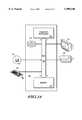
- the various methods discussed abovemay be implemented within dedicated hardware, or within processes implemented within a General Purpose Computer 120.
- the General Purpose Computer 120has a Computer Processor 122, and Memory 124, connected by a Bus 126.
- Memory 124includes relatively high speed machine readable media such as DRAM, SRAM, ROM, FLASH, EEPROM, and bubble memory.
- Secondary Storage 130includes computer readable media such as hard disk drives, magnetic drum, and bubble memory.
- External Storage 132includes computer readable media such as floppy disks, removable hard drives, magnetic tape, CD-ROM, and even other computers, possibly connected via a communications line.
- the distinction drawn here between Secondary Storage 130 and External Storage 132is primarily for convenience in describing the invention. As such, it should be appreciated that there is substantial functional overlap between these elements.
- Executable versions of computer software 133such as the LPC software utilized to implement the techniques disclosed herein and user programs are typically read from the External Storage 132 and loaded for execution directly into the Memory 124, or stored on the Secondary Storage 130 prior to loading into Memory 124 and execution.
- the physical design files 150 and LPC design files 154 utilized to make lithographic reticulesare stored on either Secondary Storage 130 or External Storage 132.
Landscapes
- Physics & Mathematics (AREA)
- General Physics & Mathematics (AREA)
- Preparing Plates And Mask In Photomechanical Process (AREA)
Abstract
Description
Claims (14)
Priority Applications (1)
| Application Number | Priority Date | Filing Date | Title |
|---|---|---|---|
| US08/805,863US5900340A (en) | 1997-03-03 | 1997-03-03 | One dimensional lithographic proximity correction using DRC shape functions |
Applications Claiming Priority (1)
| Application Number | Priority Date | Filing Date | Title |
|---|---|---|---|
| US08/805,863US5900340A (en) | 1997-03-03 | 1997-03-03 | One dimensional lithographic proximity correction using DRC shape functions |
Publications (1)
| Publication Number | Publication Date |
|---|---|
| US5900340Atrue US5900340A (en) | 1999-05-04 |
Family
ID=25192720
Family Applications (1)
| Application Number | Title | Priority Date | Filing Date |
|---|---|---|---|
| US08/805,863Expired - LifetimeUS5900340A (en) | 1997-03-03 | 1997-03-03 | One dimensional lithographic proximity correction using DRC shape functions |
Country Status (1)
| Country | Link |
|---|---|
| US (1) | US5900340A (en) |
Cited By (57)
| Publication number | Priority date | Publication date | Assignee | Title |
|---|---|---|---|---|
| US6197452B1 (en)* | 1997-09-17 | 2001-03-06 | Nec Corporation | Light exposure pattern mask with dummy patterns and production method of the same |
| US6221539B1 (en)* | 1998-07-23 | 2001-04-24 | Kabushiki Kaisha Toshiba | Mask pattern correction method and a recording medium which records a mask pattern correction program |
| US6282696B1 (en)* | 1997-08-15 | 2001-08-28 | Lsi Logic Corporation | Performing optical proximity correction with the aid of design rule checkers |
| US6335151B1 (en)* | 1999-06-18 | 2002-01-01 | International Business Machines Corporation | Micro-surface fabrication process |
| US6421820B1 (en) | 1999-12-13 | 2002-07-16 | Infineon Technologies Ag | Semiconductor device fabrication using a photomask with assist features |
| US20020199157A1 (en)* | 1999-04-30 | 2002-12-26 | Cobb Nicolas Bailey | Mixed-mode optical proximity correction |
| US6507930B1 (en)* | 2000-06-30 | 2003-01-14 | International Business Machines Corporation | Method and system for improving yield of semiconductor integrated circuits |
| US6523162B1 (en)* | 2000-08-02 | 2003-02-18 | Numerical Technologies, Inc. | General purpose shape-based layout processing scheme for IC layout modifications |
| US6553559B2 (en) | 2001-01-05 | 2003-04-22 | International Business Machines Corporation | Method to determine optical proximity correction and assist feature rules which account for variations in mask dimensions |
| US20030097647A1 (en)* | 2000-02-28 | 2003-05-22 | Numerical Technologies, Inc. | Method and apparatus for mixed-mode optical proximity correction |
| US6571383B1 (en) | 2000-04-28 | 2003-05-27 | Infineon Technologies, Ag | Semiconductor device fabrication using a photomask designed using modeling and empirical testing |
| US20030163791A1 (en)* | 2001-12-31 | 2003-08-28 | Numerical Technologies, Inc. | Shape-based geometry engine to perform smoothing and other layout beautification operations |
| US6615393B1 (en)* | 2001-06-25 | 2003-09-02 | Cypress Semiconductor Corporation | Method and apparatus for performing electrical distance check |
| US20030170565A1 (en)* | 2001-11-28 | 2003-09-11 | Eurlings Markus Franciscus Antonius | Method of removing assist features utilized to improve process latitude |
| US6649452B2 (en)* | 2002-02-28 | 2003-11-18 | Motorola, Inc. | Method for manufacturing a lithographic reticle for transferring an integrated circuit design to a semiconductor wafer |
| US6670646B2 (en) | 2002-02-11 | 2003-12-30 | Infineon Technologies Ag | Mask and method for patterning a semiconductor wafer |
| US20040053145A1 (en)* | 2000-12-30 | 2004-03-18 | Edita Tejnil | Optical assist feature for two-mask exposure lithography |
| US6709793B1 (en) | 2002-10-31 | 2004-03-23 | Motorola, Inc. | Method of manufacturing reticles using subresolution test patterns |
| US20040063000A1 (en)* | 2002-09-27 | 2004-04-01 | Mentor Graphics Corporation | Chromeless phase mask layout generation |
| US6777146B1 (en) | 2003-02-21 | 2004-08-17 | International Business Machines Corporation | Method of optical proximity correction with sub-resolution assists |
| US20040170905A1 (en)* | 2003-02-28 | 2004-09-02 | International Business Machines Corporation | Binary OPC for assist feature layout optimization |
| US20050153212A1 (en)* | 2004-01-12 | 2005-07-14 | International Business Machines Corporation | System and method of smoothing mask shapes for improved placement of sub-resolution assist features |
| US20050229131A1 (en)* | 2004-04-07 | 2005-10-13 | Shao-Po Wu | Intermediate layout for resolution enhancement in semiconductor fabrication |
| US20060248499A1 (en)* | 2005-04-29 | 2006-11-02 | Invarium, Inc. | Apparatus and method for breaking up and merging polygons |
| US20080005718A1 (en)* | 2006-06-29 | 2008-01-03 | Seth Green | Mask validation using contours |
| US20090014811A1 (en)* | 2006-03-09 | 2009-01-15 | Tela Innovations, Inc. | Dynamic Array Architecture |
| US20090032898A1 (en)* | 2007-08-02 | 2009-02-05 | Tela Innovations, Inc. | Methods for Defining Dynamic Array Section with Manufacturing Assurance Halo and Apparatus Implementing the Same |
| US20090224317A1 (en)* | 2008-03-13 | 2009-09-10 | Tela Innovations, Inc. | Cross-Coupled Transistor Layouts in Restricted Gate Level Layout Architecture |
| US20090224408A1 (en)* | 2008-03-27 | 2009-09-10 | Tela Innovations, Inc. | Methods for Multi-Wire Routing and Apparatus Implementing Same |
| US20100006901A1 (en)* | 2006-03-09 | 2010-01-14 | Tela Innovations, Inc. | Semiconductor Device Portion Having Gate Electrode Conductive Structures Formed from Rectangular Shaped Gate Electrode Layout Features Defined Along At Least Four Gate Electrode Tracks and Having Corresponding Non-Symmetric Diffusion Regions |
| US20100252896A1 (en)* | 2007-10-26 | 2010-10-07 | Tela Innovations, Inc. | Methods, Structures, and Designs for Self-Aligning Local Interconnects used in Integrated Circuits |
| US7932545B2 (en) | 2006-03-09 | 2011-04-26 | Tela Innovations, Inc. | Semiconductor device and associated layouts including gate electrode level region having arrangement of six linear conductive segments with side-to-side spacing less than 360 nanometers |
| US7979829B2 (en) | 2007-02-20 | 2011-07-12 | Tela Innovations, Inc. | Integrated circuit cell library with cell-level process compensation technique (PCT) application and associated methods |
| US8214778B2 (en) | 2007-08-02 | 2012-07-03 | Tela Innovations, Inc. | Methods for cell phasing and placement in dynamic array architecture and implementation of the same |
| US8225239B2 (en) | 2006-03-09 | 2012-07-17 | Tela Innovations, Inc. | Methods for defining and utilizing sub-resolution features in linear topology |
| US8225261B2 (en) | 2006-03-09 | 2012-07-17 | Tela Innovations, Inc. | Methods for defining contact grid in dynamic array architecture |
| US8245180B2 (en) | 2006-03-09 | 2012-08-14 | Tela Innovations, Inc. | Methods for defining and using co-optimized nanopatterns for integrated circuit design and apparatus implementing same |
| US8247846B2 (en) | 2006-03-09 | 2012-08-21 | Tela Innovations, Inc. | Oversized contacts and vias in semiconductor chip defined by linearly constrained topology |
| US8286107B2 (en) | 2007-02-20 | 2012-10-09 | Tela Innovations, Inc. | Methods and systems for process compensation technique acceleration |
| US8448102B2 (en) | 2006-03-09 | 2013-05-21 | Tela Innovations, Inc. | Optimizing layout of irregular structures in regular layout context |
| US8453094B2 (en) | 2008-01-31 | 2013-05-28 | Tela Innovations, Inc. | Enforcement of semiconductor structure regularity for localized transistors and interconnect |
| US8541879B2 (en) | 2007-12-13 | 2013-09-24 | Tela Innovations, Inc. | Super-self-aligned contacts and method for making the same |
| US8653857B2 (en) | 2006-03-09 | 2014-02-18 | Tela Innovations, Inc. | Circuitry and layouts for XOR and XNOR logic |
| US8658542B2 (en) | 2006-03-09 | 2014-02-25 | Tela Innovations, Inc. | Coarse grid design methods and structures |
| US8661392B2 (en) | 2009-10-13 | 2014-02-25 | Tela Innovations, Inc. | Methods for cell boundary encroachment and layouts implementing the Same |
| US8667443B2 (en) | 2007-03-05 | 2014-03-04 | Tela Innovations, Inc. | Integrated circuit cell library for multiple patterning |
| US8839175B2 (en) | 2006-03-09 | 2014-09-16 | Tela Innovations, Inc. | Scalable meta-data objects |
| US8863063B2 (en) | 2009-05-06 | 2014-10-14 | Tela Innovations, Inc. | Finfet transistor circuit |
| US9035359B2 (en) | 2006-03-09 | 2015-05-19 | Tela Innovations, Inc. | Semiconductor chip including region including linear-shaped conductive structures forming gate electrodes and having electrical connection areas arranged relative to inner region between transistors of different types and associated methods |
| US9122832B2 (en) | 2008-08-01 | 2015-09-01 | Tela Innovations, Inc. | Methods for controlling microloading variation in semiconductor wafer layout and fabrication |
| US9159627B2 (en) | 2010-11-12 | 2015-10-13 | Tela Innovations, Inc. | Methods for linewidth modification and apparatus implementing the same |
| US9230910B2 (en) | 2006-03-09 | 2016-01-05 | Tela Innovations, Inc. | Oversized contacts and vias in layout defined by linearly constrained topology |
| US9323882B2 (en) | 2014-03-28 | 2016-04-26 | Globalfoundries Inc. | Metrology pattern layout and method of use thereof |
| US9535319B2 (en)* | 2015-03-31 | 2017-01-03 | Globalfoundries Inc. | Reticle, system comprising a plurality of reticles and method for the formation thereof |
| US9563733B2 (en) | 2009-05-06 | 2017-02-07 | Tela Innovations, Inc. | Cell circuit and layout with linear finfet structures |
| CN106919009A (en)* | 2017-05-08 | 2017-07-04 | 上海华力微电子有限公司 | Figure preprocess method before optical near-correction |
| CN119987122A (en)* | 2025-04-16 | 2025-05-13 | 华芯程(杭州)科技有限公司 | Method, device, equipment and storage medium for making curved mask |
Citations (9)
| Publication number | Priority date | Publication date | Assignee | Title |
|---|---|---|---|---|
| US4595295A (en)* | 1982-01-06 | 1986-06-17 | International Business Machines Corporation | Alignment system for lithographic proximity printing |
| US4636626A (en)* | 1983-01-14 | 1987-01-13 | Nippon Kogaku K.K. | Apparatus for aligning mask and wafer used in semiconductor circuit element fabrication |
| US4895780A (en)* | 1987-05-13 | 1990-01-23 | General Electric Company | Adjustable windage method and mask for correction of proximity effect in submicron photolithography |
| US5208124A (en)* | 1991-03-19 | 1993-05-04 | Hewlett-Packard Company | Method of making a mask for proximity effect correction in projection lithography |
| US5242770A (en)* | 1992-01-16 | 1993-09-07 | Microunity Systems Engineering, Inc. | Mask for photolithography |
| US5447810A (en)* | 1994-02-09 | 1995-09-05 | Microunity Systems Engineering, Inc. | Masks for improved lithographic patterning for off-axis illumination lithography |
| US5546225A (en)* | 1991-08-22 | 1996-08-13 | Nikon Corporation | High resolution printing technique by using improved mask pattern and improved illumination system |
| US5636002A (en)* | 1994-04-29 | 1997-06-03 | Lucent Technologies Inc. | Auxiliary mask features for enhancing the resolution of photolithography |
| US5705301A (en)* | 1996-02-27 | 1998-01-06 | Lsi Logic Corporation | Performing optical proximity correction with the aid of design rule checkers |
- 1997
- 1997-03-03USUS08/805,863patent/US5900340A/ennot_activeExpired - Lifetime
Patent Citations (9)
| Publication number | Priority date | Publication date | Assignee | Title |
|---|---|---|---|---|
| US4595295A (en)* | 1982-01-06 | 1986-06-17 | International Business Machines Corporation | Alignment system for lithographic proximity printing |
| US4636626A (en)* | 1983-01-14 | 1987-01-13 | Nippon Kogaku K.K. | Apparatus for aligning mask and wafer used in semiconductor circuit element fabrication |
| US4895780A (en)* | 1987-05-13 | 1990-01-23 | General Electric Company | Adjustable windage method and mask for correction of proximity effect in submicron photolithography |
| US5208124A (en)* | 1991-03-19 | 1993-05-04 | Hewlett-Packard Company | Method of making a mask for proximity effect correction in projection lithography |
| US5546225A (en)* | 1991-08-22 | 1996-08-13 | Nikon Corporation | High resolution printing technique by using improved mask pattern and improved illumination system |
| US5242770A (en)* | 1992-01-16 | 1993-09-07 | Microunity Systems Engineering, Inc. | Mask for photolithography |
| US5447810A (en)* | 1994-02-09 | 1995-09-05 | Microunity Systems Engineering, Inc. | Masks for improved lithographic patterning for off-axis illumination lithography |
| US5636002A (en)* | 1994-04-29 | 1997-06-03 | Lucent Technologies Inc. | Auxiliary mask features for enhancing the resolution of photolithography |
| US5705301A (en)* | 1996-02-27 | 1998-01-06 | Lsi Logic Corporation | Performing optical proximity correction with the aid of design rule checkers |
Non-Patent Citations (2)
| Title |
|---|
| BACUS News, "Evaluation of a fast and flexible OPC Package: OPTISSMO", Society of Photo-Optical Instrumentation Engineers, vol. 13, Issue 1, pp. 3 & 5-8, Jan. (1997). |
| BACUS News, Evaluation of a fast and flexible OPC Package: OPTISSMO , Society of Photo Optical Instrumentation Engineers, vol. 13, Issue 1, pp. 3 & 5 8, Jan. (1997).* |
Cited By (269)
| Publication number | Priority date | Publication date | Assignee | Title |
|---|---|---|---|---|
| US6282696B1 (en)* | 1997-08-15 | 2001-08-28 | Lsi Logic Corporation | Performing optical proximity correction with the aid of design rule checkers |
| US6197452B1 (en)* | 1997-09-17 | 2001-03-06 | Nec Corporation | Light exposure pattern mask with dummy patterns and production method of the same |
| US6221539B1 (en)* | 1998-07-23 | 2001-04-24 | Kabushiki Kaisha Toshiba | Mask pattern correction method and a recording medium which records a mask pattern correction program |
| US20040221254A1 (en)* | 1999-04-30 | 2004-11-04 | Mentor Graphics Corporation | Mixed mode optical proximity correction |
| US20020199157A1 (en)* | 1999-04-30 | 2002-12-26 | Cobb Nicolas Bailey | Mixed-mode optical proximity correction |
| US7024655B2 (en) | 1999-04-30 | 2006-04-04 | Cobb Nicolas B | Mixed-mode optical proximity correction |
| US6335151B1 (en)* | 1999-06-18 | 2002-01-01 | International Business Machines Corporation | Micro-surface fabrication process |
| US6421820B1 (en) | 1999-12-13 | 2002-07-16 | Infineon Technologies Ag | Semiconductor device fabrication using a photomask with assist features |
| US20030097647A1 (en)* | 2000-02-28 | 2003-05-22 | Numerical Technologies, Inc. | Method and apparatus for mixed-mode optical proximity correction |
| US6584609B1 (en) | 2000-02-28 | 2003-06-24 | Numerical Technologies, Inc. | Method and apparatus for mixed-mode optical proximity correction |
| US6988259B2 (en) | 2000-02-28 | 2006-01-17 | Synopsys, Inc. | Method and apparatus for mixed-mode optical proximity correction |
| US6571383B1 (en) | 2000-04-28 | 2003-05-27 | Infineon Technologies, Ag | Semiconductor device fabrication using a photomask designed using modeling and empirical testing |
| US6507930B1 (en)* | 2000-06-30 | 2003-01-14 | International Business Machines Corporation | Method and system for improving yield of semiconductor integrated circuits |
| US6523162B1 (en)* | 2000-08-02 | 2003-02-18 | Numerical Technologies, Inc. | General purpose shape-based layout processing scheme for IC layout modifications |
| US6800406B2 (en)* | 2000-12-30 | 2004-10-05 | Intel Corporation | Method of generating optical assist features for two-mask exposure lithography |
| US20040053145A1 (en)* | 2000-12-30 | 2004-03-18 | Edita Tejnil | Optical assist feature for two-mask exposure lithography |
| US6553559B2 (en) | 2001-01-05 | 2003-04-22 | International Business Machines Corporation | Method to determine optical proximity correction and assist feature rules which account for variations in mask dimensions |
| US6615393B1 (en)* | 2001-06-25 | 2003-09-02 | Cypress Semiconductor Corporation | Method and apparatus for performing electrical distance check |
| SG103894A1 (en)* | 2001-11-28 | 2004-05-26 | Asml Masktools Bv | Method of removing assist features utilized to improve process latitude |
| CN100380233C (en)* | 2001-11-28 | 2008-04-09 | Asml蒙片工具有限公司 | Method for raising processing range with eliminating auxiliary characteristic |
| US6875545B2 (en) | 2001-11-28 | 2005-04-05 | Asml Masktools B.V. | Method of removing assist features utilized to improve process latitude |
| US20030170565A1 (en)* | 2001-11-28 | 2003-09-11 | Eurlings Markus Franciscus Antonius | Method of removing assist features utilized to improve process latitude |
| US20030163791A1 (en)* | 2001-12-31 | 2003-08-28 | Numerical Technologies, Inc. | Shape-based geometry engine to perform smoothing and other layout beautification operations |
| US7159197B2 (en) | 2001-12-31 | 2007-01-02 | Synopsys, Inc. | Shape-based geometry engine to perform smoothing and other layout beautification operations |
| US6670646B2 (en) | 2002-02-11 | 2003-12-30 | Infineon Technologies Ag | Mask and method for patterning a semiconductor wafer |
| US6649452B2 (en)* | 2002-02-28 | 2003-11-18 | Motorola, Inc. | Method for manufacturing a lithographic reticle for transferring an integrated circuit design to a semiconductor wafer |
| US20040063000A1 (en)* | 2002-09-27 | 2004-04-01 | Mentor Graphics Corporation | Chromeless phase mask layout generation |
| US7172838B2 (en) | 2002-09-27 | 2007-02-06 | Wilhelm Maurer | Chromeless phase mask layout generation |
| US6709793B1 (en) | 2002-10-31 | 2004-03-23 | Motorola, Inc. | Method of manufacturing reticles using subresolution test patterns |
| US6777146B1 (en) | 2003-02-21 | 2004-08-17 | International Business Machines Corporation | Method of optical proximity correction with sub-resolution assists |
| US20040166418A1 (en)* | 2003-02-21 | 2004-08-26 | International Business Machines Corporation | Method of optical proximity correction with sub-resolution assists |
| US20060057475A1 (en)* | 2003-02-28 | 2006-03-16 | Liebmann Lars W | Binary OPC for assist feature layout optimization |
| US7001693B2 (en) | 2003-02-28 | 2006-02-21 | International Business Machines Corporation | Binary OPC for assist feature layout optimization |
| US7147976B2 (en) | 2003-02-28 | 2006-12-12 | International Business Machines Corporation | Binary OPC for assist feature layout optimization |
| US20040170905A1 (en)* | 2003-02-28 | 2004-09-02 | International Business Machines Corporation | Binary OPC for assist feature layout optimization |
| US20050153212A1 (en)* | 2004-01-12 | 2005-07-14 | International Business Machines Corporation | System and method of smoothing mask shapes for improved placement of sub-resolution assist features |
| US7261981B2 (en)* | 2004-01-12 | 2007-08-28 | International Business Machines Corporation | System and method of smoothing mask shapes for improved placement of sub-resolution assist features |
| US20050229131A1 (en)* | 2004-04-07 | 2005-10-13 | Shao-Po Wu | Intermediate layout for resolution enhancement in semiconductor fabrication |
| US7404173B2 (en)* | 2004-04-07 | 2008-07-22 | Aprio Technologies, Inc. | Intermediate layout for resolution enhancement in semiconductor fabrication |
| US20080216047A1 (en)* | 2004-04-07 | 2008-09-04 | Aprio Technololgies, Inc. | Intermediate Layout for Resolution Enhancement in Semiconductor Fabrication |
| US7979811B2 (en) | 2004-04-07 | 2011-07-12 | Tela Innovations, Inc. | Intermediate layout for resolution enhancement in semiconductor fabrication |
| US20060248499A1 (en)* | 2005-04-29 | 2006-11-02 | Invarium, Inc. | Apparatus and method for breaking up and merging polygons |
| US7506300B2 (en)* | 2005-04-29 | 2009-03-17 | Cadence Design Systems, Inc. | Apparatus and method for breaking up and merging polygons |
| US8253173B2 (en) | 2006-03-09 | 2012-08-28 | Tela Innovations, Inc. | Semiconductor device with gate level including four transistors of first type and four transistors of second type separated by non-diffusion region and having at least two gate contacts positioned outside separating non-diffusion region |
| US8448102B2 (en) | 2006-03-09 | 2013-05-21 | Tela Innovations, Inc. | Optimizing layout of irregular structures in regular layout context |
| US10230377B2 (en) | 2006-03-09 | 2019-03-12 | Tela Innovations, Inc. | Circuitry and layouts for XOR and XNOR logic |
| US10217763B2 (en) | 2006-03-09 | 2019-02-26 | Tela Innovations, Inc. | Semiconductor chip having region including gate electrode features of rectangular shape on gate horizontal grid and first-metal structures of rectangular shape on at least eight first-metal gridlines of first-metal vertical grid |
| US10186523B2 (en) | 2006-03-09 | 2019-01-22 | Tela Innovations, Inc. | Semiconductor chip having region including gate electrode features formed in part from rectangular layout shapes on gate horizontal grid and first-metal structures formed in part from rectangular layout shapes on at least eight first-metal gridlines of first-metal vertical grid |
| US10141334B2 (en) | 2006-03-09 | 2018-11-27 | Tela Innovations, Inc. | Semiconductor chip including region having rectangular-shaped gate structures and first-metal structures |
| US20100001321A1 (en)* | 2006-03-09 | 2010-01-07 | Tela Innovations, Inc. | Semiconductor Device Layout Having Restricted Layout Region Including Rectangular Shaped Gate Electrode Layout Features Defined Along At Least Four Gate Electrode Tracks with Corresponding Non-Symmetric Diffusion Regions |
| US20100006901A1 (en)* | 2006-03-09 | 2010-01-14 | Tela Innovations, Inc. | Semiconductor Device Portion Having Gate Electrode Conductive Structures Formed from Rectangular Shaped Gate Electrode Layout Features Defined Along At Least Four Gate Electrode Tracks and Having Corresponding Non-Symmetric Diffusion Regions |
| US20100006947A1 (en)* | 2006-03-09 | 2010-01-14 | Tela Innovations, Inc. | Semiconductor Device Portion Having Sub-Wavelength-Sized Gate Electrode Conductive Structures Formed from Rectangular Shaped Gate Electrode Layout Features and Having At Least Eight Transistors |
| US20100006948A1 (en)* | 2006-03-09 | 2010-01-14 | Tela Innovations, Inc. | Semiconductor Device Portion Having Sub-193 Nanometers -Sized Gate Electrode Conductive Structures Formed from Rectangular Shaped Gate Electrode Layout Features and Having At Least Eight Transistors |
| US20100006903A1 (en)* | 2006-03-09 | 2010-01-14 | Tela Innovations, Inc. | Semiconductor Device Portion Having Sub-193 Nanometers-Sized Gate Electrode Conductive Structures Formed from Rectangular Shaped Gate Electrode Layout Features Defined Along At Least Four Gate Electrode Tracks and Having Corresponding Non-Symmetric Diffusion Regions |
| US20100011331A1 (en)* | 2006-03-09 | 2010-01-14 | Tela Innovations, Inc. | Semiconductor Device Layout Including Cell Layout Having Restricted Gate Electrode Level Layout with Linear Shaped Gate Electrode Layout Features Defined Along At Least Four Gate Electrode Tracks with Minimum End-to-End Spacing with Corresponding Non-Symmetric Diffusion Regions |
| US20100006902A1 (en)* | 2006-03-09 | 2010-01-14 | Tela Innovations, Inc. | Semiconductor Device Portion Having Sub-Wavelength-Sized Gate Electrode Conductive Structures Formed from Rectangular Shaped Gate Electrode Layout Features Defined Along At Least Four Gate Electrode Tracks and Having Corresponding Non-Symmetric Diffusion Regions |
| US20100011329A1 (en)* | 2006-03-09 | 2010-01-14 | Tela Innovations, Inc. | Semiconductor Device Layout Including Cell Layout Having Restricted Gate Electrode Level Layout with Rectangular Shaped Gate Electrode Layout Features and Equal Number of PMOS and NMOS Transistors |
| US20100006897A1 (en)* | 2006-03-09 | 2010-01-14 | Tela Innovations. Inc. | Semiconductor Device Layout Having Restricted Layout Region Including Rectangular Shaped Gate Electrode Layout Features and Equal Number of PMOS and NMOS Transistors |
| US20100006950A1 (en)* | 2006-03-09 | 2010-01-14 | Tela Innovations, Inc. | Semiconductor Device Portion Having Gate Electrode Conductive Structures Formed from Rectangular Shaped Gate Electrode Layout Features and Having At Least Eight Transistors |
| US20100017768A1 (en)* | 2006-03-09 | 2010-01-21 | Tela Innovations, Inc. | Layout of Cell of Semiconductor Device Having Rectangular Shaped Gate Electrode Layout Features Defined Along At Least Four Gate Electrode Tracks with Corresponding p-type and n-type Diffusion Regions Separated by Central Inactive Region |
| US20100012981A1 (en)* | 2006-03-09 | 2010-01-21 | Tela Innovations, Inc. | Semiconductor Device Portion Having Gate Electrode Conductive Structures Formed from Linear Shaped Gate Electrode Layout Features Defined Along At Least Four Gate Electrode Tracks with Minimum End-to-End Spacing and Having Corresponding Non-Symmetric Diffusion Regions |
| US20100023907A1 (en)* | 2006-03-09 | 2010-01-28 | Tela Innovations, Inc. | Layout of Cell of Semiconductor Device Having Linear Shaped Gate Electrode Layout Features Defined Along At Least Four Gate Electrode Tracks with Minimum End-to-End Spacing and Having Corresponding p-type and n-type Diffusion Regions Separated by Central Inactive Region |
| US20100019284A1 (en)* | 2006-03-09 | 2010-01-28 | Tela Innovations, Inc. | Cell of Semiconductor Device Having Sub-Wavelength-Sized Gate Electrode Conductive Structures Formed from Rectangular Shaped Gate Electrode Layout Features and At Least Eight Transistors |
| US20100019285A1 (en)* | 2006-03-09 | 2010-01-28 | Tela Innovations, Inc. | Cell of Semiconductor Device Having Sub-193 Nanometers-Sized Gate Electrode Conductive Structures Formed from Rectangular Shaped Gate Electrode Layout Features and At Least Eight Transistors |
| US20100019280A1 (en)* | 2006-03-09 | 2010-01-28 | Tela Innovations, Inc. | Cell of Semiconductor Device Having Gate Electrode Conductive Structures Formed from Rectangular Shaped Gate Electrode Layout Features Defined Along At Least Four Gate Electrode Tracks |
| US20100025734A1 (en)* | 2006-03-09 | 2010-02-04 | Tela Innovations, Inc. | Cell of Semiconductor Device Having Sub-Wavelength-Sized Gate Electrode Conductive Structures Formed from Linear Shaped Gate Electrode Layout Features Defined with Minimum End-to-End Spacing and Equal Number of PMOS and NMOS Transistors |
| US20100025736A1 (en)* | 2006-03-09 | 2010-02-04 | Tela Innovations, Inc. | Cell of Semiconductor Device Having Gate Electrode Conductive Structures Formed from Linear Shaped Gate Electrode Layout Features Defined with Minimum End-to-End Spacing and At Least Eight Transistors |
| US20100096671A1 (en)* | 2006-03-09 | 2010-04-22 | Tela Innovations, Inc. | Cell of Semiconductor Device Having Gate Electrode Conductive Structures Formed from Rectangular Shaped Gate Electrode Layout Features and At Least Eight Transistors |
| US10141335B2 (en) | 2006-03-09 | 2018-11-27 | Tela Innovations, Inc. | Semiconductor CIP including region having rectangular-shaped gate structures and first metal structures |
| US9917056B2 (en) | 2006-03-09 | 2018-03-13 | Tela Innovations, Inc. | Coarse grid design methods and structures |
| US7842975B2 (en) | 2006-03-09 | 2010-11-30 | Tela Innovations, Inc. | Dynamic array architecture |
| US9905576B2 (en) | 2006-03-09 | 2018-02-27 | Tela Innovations, Inc. | Semiconductor chip including region having rectangular-shaped gate structures and first metal structures |
| US9859277B2 (en) | 2006-03-09 | 2018-01-02 | Tela Innovations, Inc. | Methods, structures, and designs for self-aligning local interconnects used in integrated circuits |
| US7906801B2 (en) | 2006-03-09 | 2011-03-15 | Tela Innovations, Inc. | Semiconductor device and associated layouts having transistors formed from six linear conductive segments with intervening diffusion contact restrictions |
| US7910958B2 (en) | 2006-03-09 | 2011-03-22 | Tela Innovations, Inc. | Semiconductor device and associated layouts having transistors formed from linear conductive segment with non-active neighboring linear conductive segment |
| US7910959B2 (en) | 2006-03-09 | 2011-03-22 | Tela Innovations, Inc. | Semiconductor device and associated layouts having transistors formed from six linear conductive segments with gate electrode connection through single interconnect level |
| US9754878B2 (en) | 2006-03-09 | 2017-09-05 | Tela Innovations, Inc. | Semiconductor chip including a chip level based on a layout that includes both regular and irregular wires |
| US7923757B2 (en) | 2006-03-09 | 2011-04-12 | Tela Innovations, Inc. | Semiconductor device and associated layouts having linear shaped gate electrodes defined along at least five adjacent gate electrode tracks of equal pitch with gate electrode connection through single interconnect level |
| US7932545B2 (en) | 2006-03-09 | 2011-04-26 | Tela Innovations, Inc. | Semiconductor device and associated layouts including gate electrode level region having arrangement of six linear conductive segments with side-to-side spacing less than 360 nanometers |
| US7932544B2 (en) | 2006-03-09 | 2011-04-26 | Tela Innovations, Inc. | Semiconductor device and associated layouts including linear conductive segments having non-gate extension portions |
| US9741719B2 (en) | 2006-03-09 | 2017-08-22 | Tela Innovations, Inc. | Methods, structures, and designs for self-aligning local interconnects used in integrated circuits |
| US9711495B2 (en) | 2006-03-09 | 2017-07-18 | Tela Innovations, Inc. | Oversized contacts and vias in layout defined by linearly constrained topology |
| US7943967B2 (en) | 2006-03-09 | 2011-05-17 | Tela Innovations, Inc. | Semiconductor device and associated layouts including diffusion contact placement restriction based on relation to linear conductive segments |
| US7943966B2 (en) | 2006-03-09 | 2011-05-17 | Tela Innovations, Inc. | Integrated circuit and associated layout with gate electrode level portion including at least two complimentary transistor forming linear conductive segments and at least one non-gate linear conductive segment |
| US7948012B2 (en) | 2006-03-09 | 2011-05-24 | Tela Innovations, Inc. | Semiconductor device having 1965 nm gate electrode level region including at least four active linear conductive segments and at least one non-gate linear conductive segment |
| US7948013B2 (en) | 2006-03-09 | 2011-05-24 | Tela Innovations, Inc. | Semiconductor device and associated layouts having linear shaped gate electrodes defined along at least five adjacent gate electrode tracks of equal pitch |
| US7952119B2 (en) | 2006-03-09 | 2011-05-31 | Tela Innovations, Inc. | Semiconductor device and associated layout having three or more linear-shaped gate electrode level conductive segments of both equal length and equal pitch |
| US9673825B2 (en) | 2006-03-09 | 2017-06-06 | Tela Innovations, Inc. | Circuitry and layouts for XOR and XNOR logic |
| US20090014811A1 (en)* | 2006-03-09 | 2009-01-15 | Tela Innovations, Inc. | Dynamic Array Architecture |
| US9589091B2 (en) | 2006-03-09 | 2017-03-07 | Tela Innovations, Inc. | Scalable meta-data objects |
| US7989847B2 (en) | 2006-03-09 | 2011-08-02 | Tela Innovations, Inc. | Semiconductor device having linear-shaped gate electrodes of different transistor types with uniformity extending portions of different lengths |
| US7989848B2 (en) | 2006-03-09 | 2011-08-02 | Tela Innovations, Inc. | Semiconductor device having at least four side-by-side electrodes of equal length and equal pitch with at least two transistor connections to power or ground |
| US9443947B2 (en) | 2006-03-09 | 2016-09-13 | Tela Innovations, Inc. | Semiconductor chip including region having integrated circuit transistor gate electrodes formed by various conductive structures of specified shape and position and method for manufacturing the same |
| US8022441B2 (en) | 2006-03-09 | 2011-09-20 | Tela Innovations, Inc. | Semiconductor device and associated layouts having transistors formed from six linear conductive segments with gate electrode-to-gate electrode connection through single interconnect level and common node connection through different interconnect level |
| US8030689B2 (en) | 2006-03-09 | 2011-10-04 | Tela Innovations, Inc. | Integrated circuit device and associated layout including separated diffusion regions of different type each having four gate electrodes with each of two complementary gate electrode pairs formed from respective linear conductive segment |
| US8035133B2 (en) | 2006-03-09 | 2011-10-11 | Tela Innovations, Inc. | Semiconductor device having two pairs of transistors of different types formed from shared linear-shaped conductive features with intervening transistors of common type on equal pitch |
| US8058671B2 (en) | 2006-03-09 | 2011-11-15 | Tela Innovations, Inc. | Semiconductor device having at least three linear-shaped electrode level conductive features of equal length positioned side-by-side at equal pitch |
| US9425272B2 (en) | 2006-03-09 | 2016-08-23 | Tela Innovations, Inc. | Semiconductor chip including integrated circuit including four transistors of first transistor type and four transistors of second transistor type with electrical connections between various transistors and methods for manufacturing the same |
| US8072003B2 (en) | 2006-03-09 | 2011-12-06 | Tela Innovations, Inc. | Integrated circuit device and associated layout including two pairs of co-aligned complementary gate electrodes with offset gate contact structures |
| US8089102B2 (en) | 2006-03-09 | 2012-01-03 | Tela Innovations, Inc. | Method for fabricating integrated circuit having three or more linear-shaped gate electrode level conductive segments of both equal length and equal pitch |
| US8088682B2 (en) | 2006-03-09 | 2012-01-03 | Tela Innovations, Inc. | Method for fabricating integrated circuit with gate electrode level region including two side-by-side ones of at least three linear-shaped conductive structures electrically connected to each other through non-gate level |
| US8089100B2 (en) | 2006-03-09 | 2012-01-03 | Tela Innovations, Inc. | Integrated circuit with gate electrode level region including at least four linear-shaped conductive structures forming gate electrodes of transistors and including extending portions of at least two different sizes |
| US8089099B2 (en) | 2006-03-09 | 2012-01-03 | Tela Innovations, Inc, | Integrated circuit device and associated layout including gate electrode level region of 965 NM radius with linear-shaped conductive segments on fixed pitch |
| US8089101B2 (en) | 2006-03-09 | 2012-01-03 | Tela Innovations, Inc. | Integrated circuit device with gate electrode level region including two side-by-side ones of at least three linear-shaped conductive structures electrically connected to each other through non-gate level |
| US8088680B2 (en) | 2006-03-09 | 2012-01-03 | Tela Innovations, Inc. | Method for fabricating integrated circuit having at least three linear-shaped gate electrode level conductive features of equal length positioned side-by-side at equal pitch |
| US8088681B2 (en) | 2006-03-09 | 2012-01-03 | Tela Innovations, Inc. | Method for fabricating integrated circuit including separated diffusion regions of different type each having four gate electrodes with each of two complementary gate electrode pairs formed from respective linear condcutive segment |
| US8088679B2 (en) | 2006-03-09 | 2012-01-03 | Tela Innovations, Inc. | Method for fabricating integrated circuit with gate electrode level portion including at least two complementary transistor forming linear conductive segments and at least one non-gate linear conductive segment |
| US8089103B2 (en) | 2006-03-09 | 2012-01-03 | Tela Innovations, Inc. | Integrated circuit device with gate level region including at least three linear-shaped conductive segments having offset line ends and forming three transistors of first type and one transistor of second type |
| US8089104B2 (en) | 2006-03-09 | 2012-01-03 | Tela Innovations, Inc. | Integrated circuit with gate electrode level region including multiple linear-shaped conductive structures forming gate electrodes of transistors and including uniformity extending portions of different size |
| US8089098B2 (en) | 2006-03-09 | 2012-01-03 | Tela Innovations, Inc. | Integrated circuit device and associated layout including linear gate electrodes of different transistor types next to linear-shaped non-gate conductive segment |
| US8101975B2 (en) | 2006-03-09 | 2012-01-24 | Tela Innovations, Inc. | Integrated circuit device with gate level region including non-gate linear conductive segment positioned within 965 nanometers of four transistors of first type and four transistors of second type |
| US8110854B2 (en) | 2006-03-09 | 2012-02-07 | Tela Innovations, Inc. | Integrated circuit device with linearly defined gate electrode level region and shared diffusion region of first type connected to shared diffusion region of second type through at least two interconnect levels |
| US8129750B2 (en) | 2006-03-09 | 2012-03-06 | Tela Innovations, Inc. | Integrated circuit including at least six linear-shaped conductive structures forming gate electrodes of transistors with at least two linear-shaped conductive structures of different length |
| US8129819B2 (en) | 2006-03-09 | 2012-03-06 | Tela Innovations, Inc. | Method of fabricating integrated circuit including at least six linear-shaped conductive structures at equal pitch including at least two linear-shaped conductive structures having non-gate portions of different length |
| US8129752B2 (en) | 2006-03-09 | 2012-03-06 | Tela Innovations, Inc. | Integrated circuit including a linear-shaped conductive structure forming one gate electrode and having length greater than or equal to one-half the length of linear-shaped conductive structure forming two gate electrodes |
| US8129751B2 (en) | 2006-03-09 | 2012-03-06 | Tela Innovations, Inc. | Integrated circuit including at least six linear-shaped conductive structures forming gate electrodes and including four conductive contacting structures having at least two different connection distances |
| US8129756B2 (en) | 2006-03-09 | 2012-03-06 | Tela Innovations, Inc. | Integrated circuit including at least six linear-shaped conductive structures forming gate electrodes of transistors with at least two different extension distances beyond conductive contacting structures |
| US8129754B2 (en) | 2006-03-09 | 2012-03-06 | Tela Innovations, Inc. | Integrated circuit with gate electrode level including at least six linear-shaped conductive structures forming gate electrodes of transisters with at least one pair of linear-shaped conductive structures having offset ends |
| US8129757B2 (en) | 2006-03-09 | 2012-03-06 | Tela Innovations, Inc. | Integrated circuit including at least six linear-shaped conductive structive structures at equal pitch including at least two linear-shaped conductive structures having non-gate portions of different length |
| US8129755B2 (en) | 2006-03-09 | 2012-03-06 | Tela Innovations, Inc. | Integrated circuit with gate electrode level including at least four linear-shaped conductive structures of equal length and equal pitch with linear-shaped conductive structure forming one transistor |
| US8129753B2 (en) | 2006-03-09 | 2012-03-06 | Tela Innovations, Inc. | Integrated circuit including gate electrode level region including at least seven linear-shaped conductive structures of equal length positioned at equal pitch with at least two linear-shaped conductive structures each forming one transistor and having extending portion sized greater than gate portion |
| US8134185B2 (en) | 2006-03-09 | 2012-03-13 | Tela Innovations, Inc. | Integrated circuit having gate electrode level region including at least seven linear-shaped conductive structures at equal pitch including linear-shaped conductive structure forming transistors of two different types and at least three linear-shaped conductive structures having aligned ends |
| US8134186B2 (en) | 2006-03-09 | 2012-03-13 | Tela Innovations, Inc. | Integrated circuit including at least three linear-shaped conductive structures at equal pitch including linear-shaped conductive structure having non-gate portion length greater than gate portion length |
| US8134184B2 (en) | 2006-03-09 | 2012-03-13 | Tela Innovations, Inc. | Integrated circuit having gate electrode level region including at least four linear-shaped conductive structures with some outer-contacted linear-shaped conductive structures having larger outer extending portion than inner extending portion |
| US8134183B2 (en) | 2006-03-09 | 2012-03-13 | Tela Innovations, Inc. | Integrated circuit including linear-shaped conductive structures that have gate portions and extending portions of different size |
| US8138525B2 (en) | 2006-03-09 | 2012-03-20 | Tela Innovations, Inc. | Integrated circuit including at least three linear-shaped conductive structures of different length each forming gate of different transistor |
| US8198656B2 (en) | 2006-03-09 | 2012-06-12 | Tela Innovations, Inc. | Integrated circuit including gate electrode level region including at least four linear-shaped conductive structures of equal length having aligned ends and positioned at equal pitch and forming multiple gate electrodes of transistors of different type |
| US8207053B2 (en) | 2006-03-09 | 2012-06-26 | Tela Innovations, Inc. | Electrodes of transistors with at least two linear-shaped conductive structures of different length |
| US9425145B2 (en) | 2006-03-09 | 2016-08-23 | Tela Innovations, Inc. | Oversized contacts and vias in layout defined by linearly constrained topology |
| US8217428B2 (en) | 2006-03-09 | 2012-07-10 | Tela Innovations, Inc. | Integrated circuit including gate electrode level region including at least three linear-shaped conductive structures of equal length having aligned ends and positioned at equal pitch and forming multiple gate electrodes of transistors of different type |
| US8225239B2 (en) | 2006-03-09 | 2012-07-17 | Tela Innovations, Inc. | Methods for defining and utilizing sub-resolution features in linear topology |
| US8225261B2 (en) | 2006-03-09 | 2012-07-17 | Tela Innovations, Inc. | Methods for defining contact grid in dynamic array architecture |
| US8245180B2 (en) | 2006-03-09 | 2012-08-14 | Tela Innovations, Inc. | Methods for defining and using co-optimized nanopatterns for integrated circuit design and apparatus implementing same |
| US8247846B2 (en) | 2006-03-09 | 2012-08-21 | Tela Innovations, Inc. | Oversized contacts and vias in semiconductor chip defined by linearly constrained topology |
| US9425273B2 (en) | 2006-03-09 | 2016-08-23 | Tela Innovations, Inc. | Semiconductor chip including integrated circuit including at least five gate level conductive structures having particular spatial and electrical relationship and method for manufacturing the same |
| US8253172B2 (en) | 2006-03-09 | 2012-08-28 | Tela Innovations, Inc. | Semiconductor device with linearly restricted gate level region including four serially connected transistors of first type and four serially connected transistors of second type separated by non-diffusion region |
| US8258552B2 (en) | 2006-03-09 | 2012-09-04 | Tela Innovations, Inc. | Semiconductor device including at least six transistor forming linear shapes with at least two transistor forming linear shapes having offset ends |
| US8258548B2 (en) | 2006-03-09 | 2012-09-04 | Tela Innovations, Inc. | Semiconductor device with gate level including four transistors of first type and four transistors of second type separated by non-diffusion region with restricted gate contact placement over separating non-diffusion region |
| US9336344B2 (en) | 2006-03-09 | 2016-05-10 | Tela Innovations, Inc. | Coarse grid design methods and structures |
| US8258547B2 (en) | 2006-03-09 | 2012-09-04 | Tela Innovations, Inc. | Semiconductor device with linearly restricted gate level region including two transistors of first type and two transistors of second type with offset gate contacts |
| US8258550B2 (en) | 2006-03-09 | 2012-09-04 | Tela Innovations, Inc. | Semiconductor device including at least six transistor forming linear shapes including at least two transistor forming linear shapes having different extension distances beyond gate contact |
| US8258549B2 (en) | 2006-03-09 | 2012-09-04 | Tela Innovations, Inc. | Semiconductor device including two transistors of first type having gates formed by conductors of different length respectively aligned with two transistors of second type having gates formed by conductors of different length |
| US8258551B2 (en) | 2006-03-09 | 2012-09-04 | Tela Innovations, Inc. | Semiconductor device with gate level including transistors of first type and transistors of second type with corresponding gate contact placement restriction |
| US8264008B2 (en) | 2006-03-09 | 2012-09-11 | Tela Innovations, Inc. | Semiconductor device including transistor forming linear shapes including gate portions and extending portions of different size |
| US9240413B2 (en) | 2006-03-09 | 2016-01-19 | Tela Innovations, Inc. | Methods, structures, and designs for self-aligning local interconnects used in integrated circuits |
| US8264009B2 (en) | 2006-03-09 | 2012-09-11 | Tela Innovations, Inc. | Semiconductor device with linearly restricted gate level region including four transistors of first type and four transistors of second type with gate defining shapes of different length |
| US9230910B2 (en) | 2006-03-09 | 2016-01-05 | Tela Innovations, Inc. | Oversized contacts and vias in layout defined by linearly constrained topology |
| US8264007B2 (en) | 2006-03-09 | 2012-09-11 | Tela Innovations, Inc. | Semiconductor device including at least six transistor forming linear shapes including at least two different gate contact connection distances |
| US9035359B2 (en) | 2006-03-09 | 2015-05-19 | Tela Innovations, Inc. | Semiconductor chip including region including linear-shaped conductive structures forming gate electrodes and having electrical connection areas arranged relative to inner region between transistors of different types and associated methods |
| US9009641B2 (en) | 2006-03-09 | 2015-04-14 | Tela Innovations, Inc. | Circuits with linear finfet structures |
| US8952425B2 (en) | 2006-03-09 | 2015-02-10 | Tela Innovations, Inc. | Integrated circuit including at least four linear-shaped conductive structures having extending portions of different length |
| US8946781B2 (en) | 2006-03-09 | 2015-02-03 | Tela Innovations, Inc. | Integrated circuit including gate electrode conductive structures with different extension distances beyond contact |
| US8921897B2 (en) | 2006-03-09 | 2014-12-30 | Tela Innovations, Inc. | Integrated circuit with gate electrode conductive structures having offset ends |
| US8921896B2 (en) | 2006-03-09 | 2014-12-30 | Tela Innovations, Inc. | Integrated circuit including linear gate electrode structures having different extension distances beyond contact |
| US8839175B2 (en) | 2006-03-09 | 2014-09-16 | Tela Innovations, Inc. | Scalable meta-data objects |
| US8436400B2 (en) | 2006-03-09 | 2013-05-07 | Tela Innovations, Inc. | Semiconductor device with gate level including gate electrode conductors for transistors of first type and transistors of second type with some gate electrode conductors of different length |
| US8823062B2 (en) | 2006-03-09 | 2014-09-02 | Tela Innovations, Inc. | Integrated circuit with offset line end spacings in linear gate electrode level |
| US8658542B2 (en) | 2006-03-09 | 2014-02-25 | Tela Innovations, Inc. | Coarse grid design methods and structures |
| US8653857B2 (en) | 2006-03-09 | 2014-02-18 | Tela Innovations, Inc. | Circuitry and layouts for XOR and XNOR logic |
| US20080005718A1 (en)* | 2006-06-29 | 2008-01-03 | Seth Green | Mask validation using contours |
| US7496881B2 (en)* | 2006-06-29 | 2009-02-24 | Intel Corporation | Mask validation using contours |
| US8286107B2 (en) | 2007-02-20 | 2012-10-09 | Tela Innovations, Inc. | Methods and systems for process compensation technique acceleration |
| US7979829B2 (en) | 2007-02-20 | 2011-07-12 | Tela Innovations, Inc. | Integrated circuit cell library with cell-level process compensation technique (PCT) application and associated methods |
| US8667443B2 (en) | 2007-03-05 | 2014-03-04 | Tela Innovations, Inc. | Integrated circuit cell library for multiple patterning |
| US10074640B2 (en) | 2007-03-05 | 2018-09-11 | Tela Innovations, Inc. | Integrated circuit cell library for multiple patterning |
| US9633987B2 (en) | 2007-03-05 | 2017-04-25 | Tela Innovations, Inc. | Integrated circuit cell library for multiple patterning |
| US8966424B2 (en) | 2007-03-07 | 2015-02-24 | Tela Innovations, Inc. | Methods for cell phasing and placement in dynamic array architecture and implementation of the same |
| US9424387B2 (en) | 2007-03-07 | 2016-08-23 | Tela Innovations, Inc. | Methods for cell phasing and placement in dynamic array architecture and implementation of the same |
| US9910950B2 (en) | 2007-03-07 | 2018-03-06 | Tela Innovations, Inc. | Methods for cell phasing and placement in dynamic array architecture and implementation of the same |
| US9595515B2 (en) | 2007-03-07 | 2017-03-14 | Tela Innovations, Inc. | Semiconductor chip including integrated circuit defined within dynamic array section |
| US8756551B2 (en) | 2007-08-02 | 2014-06-17 | Tela Innovations, Inc. | Methods for designing semiconductor device with dynamic array section |
| US20090032898A1 (en)* | 2007-08-02 | 2009-02-05 | Tela Innovations, Inc. | Methods for Defining Dynamic Array Section with Manufacturing Assurance Halo and Apparatus Implementing the Same |
| US8549455B2 (en) | 2007-08-02 | 2013-10-01 | Tela Innovations, Inc. | Methods for cell phasing and placement in dynamic array architecture and implementation of the same |
| US20110108890A1 (en)* | 2007-08-02 | 2011-05-12 | Tela Innovations, Inc. | Semiconductor Device with Dynamic Array Sections Defined and Placed According to Manufacturing Assurance Halos |
| US20090032967A1 (en)* | 2007-08-02 | 2009-02-05 | Tela Innovations, Inc. | Semiconductor Device with Dynamic Array Section |
| US7908578B2 (en) | 2007-08-02 | 2011-03-15 | Tela Innovations, Inc. | Methods for designing semiconductor device with dynamic array section |
| US7888705B2 (en) | 2007-08-02 | 2011-02-15 | Tela Innovations, Inc. | Methods for defining dynamic array section with manufacturing assurance halo and apparatus implementing the same |
| US7917879B2 (en)* | 2007-08-02 | 2011-03-29 | Tela Innovations, Inc. | Semiconductor device with dynamic array section |
| US8283701B2 (en) | 2007-08-02 | 2012-10-09 | Tela Innovations, Inc. | Semiconductor device with dynamic array sections defined and placed according to manufacturing assurance halos |
| US8759882B2 (en)* | 2007-08-02 | 2014-06-24 | Tela Innovations, Inc. | Semiconductor device with dynamic array sections defined and placed according to manufacturing assurance halos |
| US8356268B2 (en) | 2007-08-02 | 2013-01-15 | Tela Innovations, Inc. | Integrated circuit device including dynamic array section with gate level having linear conductive features on at least three side-by-side lines and uniform line end spacings |
| US8214778B2 (en) | 2007-08-02 | 2012-07-03 | Tela Innovations, Inc. | Methods for cell phasing and placement in dynamic array architecture and implementation of the same |
| US8680626B2 (en) | 2007-10-26 | 2014-03-25 | Tela Innovations, Inc. | Methods, structures, and designs for self-aligning local interconnects used in integrated circuits |
| US7994545B2 (en) | 2007-10-26 | 2011-08-09 | Tela Innovations, Inc. | Methods, structures, and designs for self-aligning local interconnects used in integrated circuits |
| US20100252896A1 (en)* | 2007-10-26 | 2010-10-07 | Tela Innovations, Inc. | Methods, Structures, and Designs for Self-Aligning Local Interconnects used in Integrated Circuits |
| US10734383B2 (en) | 2007-10-26 | 2020-08-04 | Tela Innovations, Inc. | Methods, structures, and designs for self-aligning local interconnects used in integrated circuits |
| US10461081B2 (en) | 2007-12-13 | 2019-10-29 | Tel Innovations, Inc. | Super-self-aligned contacts and method for making the same |
| US9281371B2 (en) | 2007-12-13 | 2016-03-08 | Tela Innovations, Inc. | Super-self-aligned contacts and method for making the same |
| US8541879B2 (en) | 2007-12-13 | 2013-09-24 | Tela Innovations, Inc. | Super-self-aligned contacts and method for making the same |
| US8951916B2 (en) | 2007-12-13 | 2015-02-10 | Tela Innovations, Inc. | Super-self-aligned contacts and method for making the same |
| US9818747B2 (en) | 2007-12-13 | 2017-11-14 | Tela Innovations, Inc. | Super-self-aligned contacts and method for making the same |
| US9530734B2 (en) | 2008-01-31 | 2016-12-27 | Tela Innovations, Inc. | Enforcement of semiconductor structure regularity for localized transistors and interconnect |
| US9202779B2 (en) | 2008-01-31 | 2015-12-01 | Tela Innovations, Inc. | Enforcement of semiconductor structure regularity for localized transistors and interconnect |
| US8701071B2 (en) | 2008-01-31 | 2014-04-15 | Tela Innovations, Inc. | Enforcement of semiconductor structure regularity for localized transistors and interconnect |
| US8453094B2 (en) | 2008-01-31 | 2013-05-28 | Tela Innovations, Inc. | Enforcement of semiconductor structure regularity for localized transistors and interconnect |
| US9117050B2 (en) | 2008-03-13 | 2015-08-25 | Tela Innovations, Inc. | Integrated circuit including cross-coupled transistors having gate electrodes formed within gate level feature layout channels with gate contact position and offset specifications |
| US8581303B2 (en) | 2008-03-13 | 2013-11-12 | Tela Innovations, Inc. | Integrated circuit including cross-coupled trasistors having gate electrodes formed within gate level feature layout channels with four inside positioned gate contacts having offset relationships and electrical connection of cross-coupled transistors through same interconnect layer |
| US8847331B2 (en) | 2008-03-13 | 2014-09-30 | Tela Innovations, Inc. | Semiconductor chip including region having cross-coupled transistor configuration with offset electrical connection areas on gate electrode forming conductive structures and at least two different inner extension distances of gate electrode forming conductive structures |
| US8847329B2 (en) | 2008-03-13 | 2014-09-30 | Tela Innovations, Inc. | Cross-coupled transistor circuit defined having diffusion regions of common node on opposing sides of same gate electrode track with at least two non-inner positioned gate contacts |
| US8853794B2 (en) | 2008-03-13 | 2014-10-07 | Tela Innovations, Inc. | Integrated circuit within semiconductor chip including cross-coupled transistor configuration |
| US8853793B2 (en) | 2008-03-13 | 2014-10-07 | Tela Innovations, Inc. | Integrated circuit including gate electrode level region including cross-coupled transistors having gate contacts located over inner portion of gate electrode level region and offset gate level feature line ends |
| US8552509B2 (en) | 2008-03-13 | 2013-10-08 | Tela Innovations, Inc. | Integrated circuit including cross-coupled transistors having gate electrodes formed within gate level feature layout channels with other transistors positioned between cross-coupled transistors |
| US8866197B2 (en) | 2008-03-13 | 2014-10-21 | Tela Innovations, Inc. | Integrated circuit including cross-coupled transistors having gate electrodes formed within gate level feature layout channels with at least two gate electrodes electrically connected to each other through another transistor forming gate level feature |
| US8872283B2 (en) | 2008-03-13 | 2014-10-28 | Tela Innovations, Inc. | Integrated circuit including cross-coupled transistors having gate electrodes formed within gate level feature layout channels with shared diffusion regions on opposite sides of two-transistor-forming gate level feature |
| US8405162B2 (en) | 2008-03-13 | 2013-03-26 | Tela Innovations, Inc. | Integrated circuit including gate electrode level region including cross-coupled transistors having at least one gate contact located over outer portion of gate electrode level region |
| US8395224B2 (en) | 2008-03-13 | 2013-03-12 | Tela Innovations, Inc. | Linear gate level cross-coupled transistor device with non-overlapping PMOS transistors and non-overlapping NMOS transistors relative to directions of gate electrodes |
| US8835989B2 (en) | 2008-03-13 | 2014-09-16 | Tela Innovations, Inc. | Integrated circuit including cross-coupled transistors having gate electrodes formed within gate level feature layout channels with gate electrode placement specifications |
| US8405163B2 (en) | 2008-03-13 | 2013-03-26 | Tela Innovations, Inc. | Integrated circuit including cross-coupled transistors having gate electrodes formed within gate level feature layout channels with shared diffusion regions on opposite sides of two-transistor-forming gate level feature |
| US8816402B2 (en) | 2008-03-13 | 2014-08-26 | Tela Innovations, Inc. | Integrated circuit including cross-coupled transistors having gate electrodes formed within gate level feature layout channels with gate level feature layout channel including single transistor |
| US8785979B2 (en) | 2008-03-13 | 2014-07-22 | Tela Innovations, Inc. | Integrated circuit including cross-coupled transistors having gate electrodes formed within gate level feature layout channels with two inside positioned gate contacts and two outside positioned gate contacts and electrical connection of cross-coupled transistors through same interconnect layer |
| US8785978B2 (en) | 2008-03-13 | 2014-07-22 | Tela Innovations, Inc. | Integrated circuit including cross-coupled transistors having gate electrodes formed within gate level feature layout channels with electrical connection of cross-coupled transistors through same interconnect layer |
| US8274099B2 (en) | 2008-03-13 | 2012-09-25 | Tela Innovations, Inc. | Integrated circuit including cross-coupled transistors having gate electrodes formed within gate level feature layout channels with gate contact position and offset specifications |
| US9081931B2 (en) | 2008-03-13 | 2015-07-14 | Tela Innovations, Inc. | Cross-coupled transistor circuit having diffusion regions of common node on opposing sides of same gate electrode track and gate node connection through single interconnect layer |
| US8772839B2 (en) | 2008-03-13 | 2014-07-08 | Tela Innovations, Inc. | Integrated circuit including cross-coupled transistors having gate electrodes formed within gate level feature layout channels with four inside positioned gate contacts having offset and aligned relationships and electrical connection of transistor gates through linear interconnect conductors in single interconnect layer |
| US10727252B2 (en) | 2008-03-13 | 2020-07-28 | Tela Innovations, Inc. | Semiconductor chip including integrated circuit having cross-coupled transistor configuration and method for manufacturing the same |
| US10658385B2 (en) | 2008-03-13 | 2020-05-19 | Tela Innovations, Inc. | Cross-coupled transistor circuit defined on four gate electrode tracks |
| US10651200B2 (en) | 2008-03-13 | 2020-05-12 | Tela Innovations, Inc. | Cross-coupled transistor circuit defined on three gate electrode tracks |
| US9208279B2 (en) | 2008-03-13 | 2015-12-08 | Tela Innovations, Inc. | Semiconductor chip including digital logic circuit including linear-shaped conductive structures having electrical connection areas located within inner region between transistors of different type and associated methods |
| US9213792B2 (en) | 2008-03-13 | 2015-12-15 | Tela Innovations, Inc. | Semiconductor chip including digital logic circuit including at least six transistors with some transistors forming cross-coupled transistor configuration and associated methods |
| US8264049B2 (en) | 2008-03-13 | 2012-09-11 | Tela Innovations, Inc. | Integrated circuit including cross-coupled transistors with two transistors of different type having gate electrodes formed by common gate level feature with shared diffusion regions on opposite sides of common gate level feature |
| US8264044B2 (en) | 2008-03-13 | 2012-09-11 | Tela Innovations, Inc. | Integrated circuit including cross-coupled transistors having two complementary pairs of co-aligned gate electrodes with offset contacting structures positioned between transistors of different type |
| US9245081B2 (en) | 2008-03-13 | 2016-01-26 | Tela Innovations, Inc. | Semiconductor chip including digital logic circuit including at least nine linear-shaped conductive structures collectively forming gate electrodes of at least six transistors with some transistors forming cross-coupled transistor configuration and associated methods |
| US8552508B2 (en) | 2008-03-13 | 2013-10-08 | Tela Innovations, Inc. | Integrated circuit including cross-coupled transistors having gate electrodes formed within gate level feature layout channels with shared diffusion regions on opposite sides of two-transistor-forming gate level feature and electrical connection of transistor gates through linear interconnect conductors in single interconnect layer |
| US8742463B2 (en) | 2008-03-13 | 2014-06-03 | Tela Innovations, Inc. | Integrated circuit including cross-coupled transistors having gate electrodes formed within gate level feature layout channels with outer positioned gate contacts |
| US8558322B2 (en) | 2008-03-13 | 2013-10-15 | Tela Innovations, Inc. | Integrated circuit including cross-coupled transistors having gate electrodes formed within gate level feature layout channels with at least two gate electrodes electrically connected to each other through gate level feature |
| US8258581B2 (en) | 2008-03-13 | 2012-09-04 | Tela Innovations, Inc. | Integrated circuit including cross-coupled transistors with two transistors of different type formed by same gate level structure and two transistors of different type formed by separate gate level structures |
| US8564071B2 (en) | 2008-03-13 | 2013-10-22 | Tela Innovations, Inc. | Integrated circuit including cross-coupled transistors having gate electrodes formed within gate level feature layout channels with at least two different gate level feature extensions beyond contact |
| US8742462B2 (en) | 2008-03-13 | 2014-06-03 | Tela Innovations, Inc. | Integrated circuit including cross-coupled transistors having gate electrodes formed within gate level feature layout channels with gate contact position specifications |
| US8735944B2 (en) | 2008-03-13 | 2014-05-27 | Tela Innovations, Inc. | Integrated circuit including cross-coupled transistors having gate electrodes formed within gate level feature layout channels with serially connected transistors |
| US8058691B2 (en) | 2008-03-13 | 2011-11-15 | Tela Innovations, Inc. | Semiconductor device including cross-coupled transistors formed from linear-shaped gate level features |
| US8735995B2 (en) | 2008-03-13 | 2014-05-27 | Tela Innovations, Inc. | Cross-coupled transistor circuit defined on three gate electrode tracks with diffusion regions of common node on opposing sides of same gate electrode track |
| US8729643B2 (en) | 2008-03-13 | 2014-05-20 | Tela Innovations, Inc. | Cross-coupled transistor circuit including offset inner gate contacts |
| US20090224317A1 (en)* | 2008-03-13 | 2009-09-10 | Tela Innovations, Inc. | Cross-Coupled Transistor Layouts in Restricted Gate Level Layout Architecture |
| US8729606B2 (en) | 2008-03-13 | 2014-05-20 | Tela Innovations, Inc. | Integrated circuit including cross-coupled transistors having gate electrodes formed within gate level feature layout channels |
| US20100252889A1 (en)* | 2008-03-13 | 2010-10-07 | Tela Innovations, Inc. | Linear Gate Level Cross-Coupled Transistor Device with Contiguous p-type Diffusion Regions and Contiguous n-type Diffusion Regions |
| US9536899B2 (en) | 2008-03-13 | 2017-01-03 | Tela Innovations, Inc. | Semiconductor chip including integrated circuit having cross-coupled transistor configuration and method for manufacturing the same |
| US8569841B2 (en) | 2008-03-13 | 2013-10-29 | Tela Innovations, Inc. | Integrated circuit including cross-coupled transistors having gate electrodes formed within gate level feature layout channels with at least one gate level feature extending into adjacent gate level feature layout channel |
| US8680583B2 (en) | 2008-03-13 | 2014-03-25 | Tela Innovations, Inc. | Integrated circuit including cross-coupled transistors having gate electrodes formed within at least nine gate level feature layout channels |
| US8669594B2 (en) | 2008-03-13 | 2014-03-11 | Tela Innovations, Inc. | Integrated circuit including cross-coupled transistors having gate electrodes formed within at least twelve gate level feature layout channels |
| US8669595B2 (en) | 2008-03-13 | 2014-03-11 | Tela Innovations, Inc. | Integrated circuit including cross-coupled transistors having gate electrodes formed within gate level feature layout channels with gate contact position, alignment, and offset specifications |
| US7956421B2 (en) | 2008-03-13 | 2011-06-07 | Tela Innovations, Inc. | Cross-coupled transistor layouts in restricted gate level layout architecture |
| US10020321B2 (en) | 2008-03-13 | 2018-07-10 | Tela Innovations, Inc. | Cross-coupled transistor circuit defined on two gate electrode tracks |
| US8575706B2 (en) | 2008-03-13 | 2013-11-05 | Tela Innovations, Inc. | Integrated circuit including cross-coupled transistors having gate electrodes formed within gate level feature layout channels with at least two different gate level features inner extensions beyond gate electrode |
| US8581304B2 (en) | 2008-03-13 | 2013-11-12 | Tela Innovations, Inc. | Integrated circuit including cross-coupled transistors having gate electrodes formed within gate level feature layout channels with four inside positioned gate contacts having offset and aligned relationships |
| US8836045B2 (en) | 2008-03-13 | 2014-09-16 | Tela Innovations, Inc. | Cross-coupled transistor circuit having diffusion regions of common node on opposing sides of same gate electrode track |
| US9871056B2 (en) | 2008-03-13 | 2018-01-16 | Tela Innovations, Inc. | Semiconductor chip including integrated circuit having cross-coupled transistor configuration and method for manufacturing the same |
| US8587034B2 (en) | 2008-03-13 | 2013-11-19 | Tela Innovations, Inc. | Integrated circuit including cross-coupled transistors having gate electrodes formed within gate level feature layout channels with four inside positioned gate contacts and electrical connection of transistor gates through linear interconnect conductors in single interconnect layer |
| US8592872B2 (en) | 2008-03-13 | 2013-11-26 | Tela Innovations, Inc. | Integrated circuit including cross-coupled transistors with two transistors of different type having gate electrodes formed by common gate level feature with shared diffusion regions on opposite sides of common gate level feature |
| US9390215B2 (en) | 2008-03-27 | 2016-07-12 | Tela Innovations, Inc. | Methods for multi-wire routing and apparatus implementing same |
| US8471391B2 (en) | 2008-03-27 | 2013-06-25 | Tela Innovations, Inc. | Methods for multi-wire routing and apparatus implementing same |
| US7939443B2 (en) | 2008-03-27 | 2011-05-10 | Tela Innovations, Inc. | Methods for multi-wire routing and apparatus implementing same |
| US8759985B2 (en) | 2008-03-27 | 2014-06-24 | Tela Innovations, Inc. | Methods for multi-wire routing and apparatus implementing same |
| US9779200B2 (en) | 2008-03-27 | 2017-10-03 | Tela Innovations, Inc. | Methods for multi-wire routing and apparatus implementing same |
| US20090224408A1 (en)* | 2008-03-27 | 2009-09-10 | Tela Innovations, Inc. | Methods for Multi-Wire Routing and Apparatus Implementing Same |
| US9122832B2 (en) | 2008-08-01 | 2015-09-01 | Tela Innovations, Inc. | Methods for controlling microloading variation in semiconductor wafer layout and fabrication |
| US8863063B2 (en) | 2009-05-06 | 2014-10-14 | Tela Innovations, Inc. | Finfet transistor circuit |
| US9563733B2 (en) | 2009-05-06 | 2017-02-07 | Tela Innovations, Inc. | Cell circuit and layout with linear finfet structures |
| US10446536B2 (en) | 2009-05-06 | 2019-10-15 | Tela Innovations, Inc. | Cell circuit and layout with linear finfet structures |
| US9269702B2 (en) | 2009-10-13 | 2016-02-23 | Tela Innovations, Inc. | Methods for cell boundary encroachment and layouts implementing the same |
| US9530795B2 (en) | 2009-10-13 | 2016-12-27 | Tela Innovations, Inc. | Methods for cell boundary encroachment and semiconductor devices implementing the same |
| US8661392B2 (en) | 2009-10-13 | 2014-02-25 | Tela Innovations, Inc. | Methods for cell boundary encroachment and layouts implementing the Same |
| US9704845B2 (en) | 2010-11-12 | 2017-07-11 | Tela Innovations, Inc. | Methods for linewidth modification and apparatus implementing the same |
| US9159627B2 (en) | 2010-11-12 | 2015-10-13 | Tela Innovations, Inc. | Methods for linewidth modification and apparatus implementing the same |
| US9323882B2 (en) | 2014-03-28 | 2016-04-26 | Globalfoundries Inc. | Metrology pattern layout and method of use thereof |
| US9864831B2 (en) | 2014-03-28 | 2018-01-09 | Globalfoundries Inc. | Metrology pattern layout and method of use thereof |
| US9535319B2 (en)* | 2015-03-31 | 2017-01-03 | Globalfoundries Inc. | Reticle, system comprising a plurality of reticles and method for the formation thereof |
| CN106919009B (en)* | 2017-05-08 | 2019-05-03 | 上海华力微电子有限公司 | Figure preprocess method before optical near-correction |
| CN106919009A (en)* | 2017-05-08 | 2017-07-04 | 上海华力微电子有限公司 | Figure preprocess method before optical near-correction |
| CN119987122A (en)* | 2025-04-16 | 2025-05-13 | 华芯程(杭州)科技有限公司 | Method, device, equipment and storage medium for making curved mask |
Similar Documents
| Publication | Publication Date | Title |
|---|---|---|
| US5900340A (en) | One dimensional lithographic proximity correction using DRC shape functions | |
| US5920487A (en) | Two dimensional lithographic proximity correction using DRC shape functions | |
| US7337421B2 (en) | Method and system for managing design corrections for optical and process effects based on feature tolerances | |
| US5553274A (en) | Vertex minimization in a smart optical proximity correction system | |
| US6470489B1 (en) | Design rule checking system and method | |
| US5657235A (en) | Continuous scale optical proximity correction by mask maker dose modulation | |
| US8732625B2 (en) | Methods for performing model-based lithography guided layout design | |
| US7882480B2 (en) | System and method for model-based sub-resolution assist feature generation | |
| US6453452B1 (en) | Method and apparatus for data hierarchy maintenance in a system for mask description | |
| US7759027B2 (en) | Method and system for design of a reticle to be manufactured using character projection lithography | |
| US7306881B2 (en) | Method and system of lithography using masks having gray-tone features | |
| US9038002B2 (en) | Method and system for semiconductor design hierarchy analysis and transformation | |
| US5958635A (en) | Lithographic proximity correction through subset feature modification | |
| EP1023640B1 (en) | Data hierarchy layout correction and verification method and apparatus | |
| US20030192013A1 (en) | Method and apparatus for facilitating process-compliant layout optimization | |
| US7901845B2 (en) | Method for optical proximity correction of a reticle to be manufactured using character projection lithography | |
| WO1999014638A1 (en) | Design rule checking system and method | |
| US8713488B2 (en) | Layout design defect repair based on inverse lithography and traditional optical proximity correction | |
| US6218089B1 (en) | Photolithographic method | |
| US7745078B2 (en) | Method and system for manufacturing a reticle using character projection lithography | |
| US9779186B2 (en) | Methods for performing model-based lithography guided layout design | |
| US8788982B2 (en) | Layout design defect repair using inverse lithography | |
| US12254258B2 (en) | Critical dimension uniformity | |
| US12118287B2 (en) | Automatic generation of sub-cells for an analog integrated circuit | |
| US6413685B1 (en) | Method of reducing optical proximity effect |
Legal Events
| Date | Code | Title | Description |
|---|---|---|---|
| AS | Assignment | Owner name:MOTOROLA, INC., ILLINOIS Free format text:ASSIGNMENT OF ASSIGNORS INTEREST;ASSIGNORS:REICH, ALFRED J.;LUCAS, KEVIN D.;KLING, MICHAEL E.;AND OTHERS;REEL/FRAME:008410/0878 Effective date:19970225 | |
| STCF | Information on status: patent grant | Free format text:PATENTED CASE | |
| FPAY | Fee payment | Year of fee payment:4 | |
| AS | Assignment | Owner name:FREESCALE SEMICONDUCTOR, INC., TEXAS Free format text:ASSIGNMENT OF ASSIGNORS INTEREST;ASSIGNOR:MOTOROLA, INC.;REEL/FRAME:015698/0657 Effective date:20040404 Owner name:FREESCALE SEMICONDUCTOR, INC.,TEXAS Free format text:ASSIGNMENT OF ASSIGNORS INTEREST;ASSIGNOR:MOTOROLA, INC.;REEL/FRAME:015698/0657 Effective date:20040404 | |
| FPAY | Fee payment | Year of fee payment:8 | |
| AS | Assignment | Owner name:CITIBANK, N.A. AS COLLATERAL AGENT, NEW YORK Free format text:SECURITY AGREEMENT;ASSIGNORS:FREESCALE SEMICONDUCTOR, INC.;FREESCALE ACQUISITION CORPORATION;FREESCALE ACQUISITION HOLDINGS CORP.;AND OTHERS;REEL/FRAME:018855/0129 Effective date:20061201 Owner name:CITIBANK, N.A. AS COLLATERAL AGENT,NEW YORK Free format text:SECURITY AGREEMENT;ASSIGNORS:FREESCALE SEMICONDUCTOR, INC.;FREESCALE ACQUISITION CORPORATION;FREESCALE ACQUISITION HOLDINGS CORP.;AND OTHERS;REEL/FRAME:018855/0129 Effective date:20061201 | |
| AS | Assignment | Owner name:CITIBANK, N.A., AS COLLATERAL AGENT,NEW YORK Free format text:SECURITY AGREEMENT;ASSIGNOR:FREESCALE SEMICONDUCTOR, INC.;REEL/FRAME:024397/0001 Effective date:20100413 Owner name:CITIBANK, N.A., AS COLLATERAL AGENT, NEW YORK Free format text:SECURITY AGREEMENT;ASSIGNOR:FREESCALE SEMICONDUCTOR, INC.;REEL/FRAME:024397/0001 Effective date:20100413 | |
| FPAY | Fee payment | Year of fee payment:12 | |
| AS | Assignment | Owner name:CITIBANK, N.A., AS NOTES COLLATERAL AGENT, NEW YORK Free format text:SECURITY AGREEMENT;ASSIGNOR:FREESCALE SEMICONDUCTOR, INC.;REEL/FRAME:030633/0424 Effective date:20130521 Owner name:CITIBANK, N.A., AS NOTES COLLATERAL AGENT, NEW YOR Free format text:SECURITY AGREEMENT;ASSIGNOR:FREESCALE SEMICONDUCTOR, INC.;REEL/FRAME:030633/0424 Effective date:20130521 | |
| AS | Assignment | Owner name:CITIBANK, N.A., AS NOTES COLLATERAL AGENT, NEW YORK Free format text:SECURITY AGREEMENT;ASSIGNOR:FREESCALE SEMICONDUCTOR, INC.;REEL/FRAME:031591/0266 Effective date:20131101 Owner name:CITIBANK, N.A., AS NOTES COLLATERAL AGENT, NEW YOR Free format text:SECURITY AGREEMENT;ASSIGNOR:FREESCALE SEMICONDUCTOR, INC.;REEL/FRAME:031591/0266 Effective date:20131101 | |
| AS | Assignment | Owner name:FREESCALE SEMICONDUCTOR, INC., TEXAS Free format text:PATENT RELEASE;ASSIGNOR:CITIBANK, N.A., AS COLLATERAL AGENT;REEL/FRAME:037354/0225 Effective date:20151207 Owner name:FREESCALE SEMICONDUCTOR, INC., TEXAS Free format text:PATENT RELEASE;ASSIGNOR:CITIBANK, N.A., AS COLLATERAL AGENT;REEL/FRAME:037356/0553 Effective date:20151207 Owner name:FREESCALE SEMICONDUCTOR, INC., TEXAS Free format text:PATENT RELEASE;ASSIGNOR:CITIBANK, N.A., AS COLLATERAL AGENT;REEL/FRAME:037356/0143 Effective date:20151207 | |
| AS | Assignment | Owner name:MORGAN STANLEY SENIOR FUNDING, INC., MARYLAND Free format text:ASSIGNMENT AND ASSUMPTION OF SECURITY INTEREST IN PATENTS;ASSIGNOR:CITIBANK, N.A.;REEL/FRAME:037486/0517 Effective date:20151207 | |
| AS | Assignment | Owner name:MORGAN STANLEY SENIOR FUNDING, INC., MARYLAND Free format text:ASSIGNMENT AND ASSUMPTION OF SECURITY INTEREST IN PATENTS;ASSIGNOR:CITIBANK, N.A.;REEL/FRAME:037518/0292 Effective date:20151207 | |
| AS | Assignment | Owner name:MORGAN STANLEY SENIOR FUNDING, INC., MARYLAND Free format text:SUPPLEMENT TO THE SECURITY AGREEMENT;ASSIGNOR:FREESCALE SEMICONDUCTOR, INC.;REEL/FRAME:039138/0001 Effective date:20160525 | |
| AS | Assignment | Owner name:NXP, B.V., F/K/A FREESCALE SEMICONDUCTOR, INC., NETHERLANDS Free format text:RELEASE BY SECURED PARTY;ASSIGNOR:MORGAN STANLEY SENIOR FUNDING, INC.;REEL/FRAME:040925/0001 Effective date:20160912 Owner name:NXP, B.V., F/K/A FREESCALE SEMICONDUCTOR, INC., NE Free format text:RELEASE BY SECURED PARTY;ASSIGNOR:MORGAN STANLEY SENIOR FUNDING, INC.;REEL/FRAME:040925/0001 Effective date:20160912 | |
| AS | Assignment | Owner name:NXP B.V., NETHERLANDS Free format text:RELEASE BY SECURED PARTY;ASSIGNOR:MORGAN STANLEY SENIOR FUNDING, INC.;REEL/FRAME:040928/0001 Effective date:20160622 | |
| AS | Assignment | Owner name:NXP USA, INC., TEXAS Free format text:CHANGE OF NAME;ASSIGNOR:FREESCALE SEMICONDUCTOR INC.;REEL/FRAME:040652/0180 Effective date:20161107 | |
| AS | Assignment | Owner name:NXP USA, INC., TEXAS Free format text:CORRECTIVE ASSIGNMENT TO CORRECT THE NATURE OF CONVEYANCE LISTED CHANGE OF NAME SHOULD BE MERGER AND CHANGE PREVIOUSLY RECORDED AT REEL: 040652 FRAME: 0180. ASSIGNOR(S) HEREBY CONFIRMS THE MERGER AND CHANGE OF NAME;ASSIGNOR:FREESCALE SEMICONDUCTOR INC.;REEL/FRAME:041354/0148 Effective date:20161107 | |
| AS | Assignment | Owner name:MORGAN STANLEY SENIOR FUNDING, INC., MARYLAND Free format text:CORRECTIVE ASSIGNMENT TO CORRECT THE REMOVE PATENTS 8108266 AND 8062324 AND REPLACE THEM WITH 6108266 AND 8060324 PREVIOUSLY RECORDED ON REEL 037518 FRAME 0292. ASSIGNOR(S) HEREBY CONFIRMS THE ASSIGNMENT AND ASSUMPTION OF SECURITY INTEREST IN PATENTS;ASSIGNOR:CITIBANK, N.A.;REEL/FRAME:041703/0536 Effective date:20151207 | |
| AS | Assignment | Owner name:SHENZHEN XINGUODU TECHNOLOGY CO., LTD., CHINA Free format text:CORRECTIVE ASSIGNMENT TO CORRECT THE TO CORRECT THE APPLICATION NO. FROM 13,883,290 TO 13,833,290 PREVIOUSLY RECORDED ON REEL 041703 FRAME 0536. ASSIGNOR(S) HEREBY CONFIRMS THE THE ASSIGNMENT AND ASSUMPTION OF SECURITYINTEREST IN PATENTS.;ASSIGNOR:MORGAN STANLEY SENIOR FUNDING, INC.;REEL/FRAME:048734/0001 Effective date:20190217 | |
| AS | Assignment | Owner name:NXP B.V., NETHERLANDS Free format text:RELEASE BY SECURED PARTY;ASSIGNOR:MORGAN STANLEY SENIOR FUNDING, INC.;REEL/FRAME:050744/0097 Effective date:20190903 | |
| AS | Assignment | Owner name:MORGAN STANLEY SENIOR FUNDING, INC., MARYLAND Free format text:CORRECTIVE ASSIGNMENT TO CORRECT THE REMOVE APPLICATION11759915 AND REPLACE IT WITH APPLICATION 11759935 PREVIOUSLY RECORDED ON REEL 037486 FRAME 0517. ASSIGNOR(S) HEREBY CONFIRMS THE ASSIGNMENT AND ASSUMPTION OF SECURITYINTEREST IN PATENTS;ASSIGNOR:CITIBANK, N.A.;REEL/FRAME:053547/0421 Effective date:20151207 | |
| AS | Assignment | Owner name:NXP B.V., NETHERLANDS Free format text:CORRECTIVE ASSIGNMENT TO CORRECT THE REMOVEAPPLICATION 11759915 AND REPLACE IT WITH APPLICATION11759935 PREVIOUSLY RECORDED ON REEL 040928 FRAME 0001. ASSIGNOR(S) HEREBY CONFIRMS THE RELEASE OF SECURITYINTEREST;ASSIGNOR:MORGAN STANLEY SENIOR FUNDING, INC.;REEL/FRAME:052915/0001 Effective date:20160622 | |
| AS | Assignment | Owner name:NXP, B.V. F/K/A FREESCALE SEMICONDUCTOR, INC., NETHERLANDS Free format text:CORRECTIVE ASSIGNMENT TO CORRECT THE REMOVEAPPLICATION 11759915 AND REPLACE IT WITH APPLICATION11759935 PREVIOUSLY RECORDED ON REEL 040925 FRAME 0001. ASSIGNOR(S) HEREBY CONFIRMS THE RELEASE OF SECURITYINTEREST;ASSIGNOR:MORGAN STANLEY SENIOR FUNDING, INC.;REEL/FRAME:052917/0001 Effective date:20160912 |