US5898633A - Circuit and method of limiting leakage current in a memory circuit - Google Patents
Circuit and method of limiting leakage current in a memory circuitDownload PDFInfo
- Publication number
- US5898633A US5898633AUS08/859,897US85989797AUS5898633AUS 5898633 AUS5898633 AUS 5898633AUS 85989797 AUS85989797 AUS 85989797AUS 5898633 AUS5898633 AUS 5898633A
- Authority
- US
- United States
- Prior art keywords
- mosfet
- circuit
- current
- semiconductor
- semiconductor region
- Prior art date
- Legal status (The legal status is an assumption and is not a legal conclusion. Google has not performed a legal analysis and makes no representation as to the accuracy of the status listed.)
- Expired - Lifetime
Links
Images
Classifications
- G—PHYSICS
- G11—INFORMATION STORAGE
- G11C—STATIC STORES
- G11C11/00—Digital stores characterised by the use of particular electric or magnetic storage elements; Storage elements therefor
- G11C11/21—Digital stores characterised by the use of particular electric or magnetic storage elements; Storage elements therefor using electric elements
- G11C11/34—Digital stores characterised by the use of particular electric or magnetic storage elements; Storage elements therefor using electric elements using semiconductor devices
- G11C11/40—Digital stores characterised by the use of particular electric or magnetic storage elements; Storage elements therefor using electric elements using semiconductor devices using transistors
- G—PHYSICS
- G11—INFORMATION STORAGE
- G11C—STATIC STORES
- G11C16/00—Erasable programmable read-only memories
- G11C16/02—Erasable programmable read-only memories electrically programmable
- G11C16/06—Auxiliary circuits, e.g. for writing into memory
- G11C16/30—Power supply circuits
Definitions
- the present inventionrelates, in general, to integrated circuits and, more particularly, to current limiting circuits.
- a portable wireless systemsuch as a cellular phone or a pager uses analog and active circuitry to convert signals between frequencies ranging from radio frequency (RF) to base band. Received RF signals are converted to base-band signals through circuits such as an RF transceiver, a down converter, and a demodulator. In the case of a cellular phone, the converted base-band signals are processed into recognizable speech in the voice band frequencies.
- the portable wireless systemtypically draws its operating power from a battery source. Analog and active circuitry in the portable wireless system are primary sources of battery current drain during system operation.
- the transistors of the analog and active circuitryhave well regions formed in a substrate of the integrated circuit.
- the reverse-biased PN-junction diodes formed by the well regions in the substratehave leakage currents based on the junction area of the diodes.
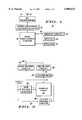
- FIG. 1is a block diagram of a wireless communication device
- FIG. 2is a block diagram of a memory circuit in the wireless communication device
- FIG. 3is a schematic diagram of a memory cell of the memory circuit
- FIG. 4is a cross-sectional view of the memory cell and a current limiting circuit
- FIGS. 5-9are embodiments of the current limiting circuit.
- the present inventionprovides a circuit and method for current limiting the memory cells of a memory array in a portable wireless system while operating in a standby mode.
- the portable wireless communication systemdraws its supply voltage from a local battery source.
- Analog and active circuitryare primary sources of current drain during normal system operation. However, in the standby mode active circuitry is disabled and the leakage currents from the well regions associated with the transistors of the integrated circuit are the primary source of current drain that diminishes battery life.
- the portable wireless systemtypically operates in the standby mode for a high percentage of the time. Thus, the current limiting circuit is switched off during the standby mode to limit the semiconductor well leakage currents and prolong the life of the battery.
- FIG. 1is a block diagram of a wireless communication device 10 such as a cellular telephone or a two-way radio.
- Wireless communication device 10includes an antenna 12, an RF transceiver 14 (transmitter circuit and a receiver circuit), a down converter and demodulator circuit 16, a data processing circuit 18, a speaker 20, a keypad 22, and a memory circuit 24.
- Antenna 12receives a transmitted radio frequency carrier signal modulated with digital information.
- RF transceiver 14amplifies the RF carrier signal and converts the frequency down to an intermediate frequency (IF) signal which is coupled to an input of a down converter and demodulator circuit 16.
- IFintermediate frequency
- RF transceiver 14is also referred to as a translator that is coupled for receiving a transmitted signal.
- Down converter and demodulator circuit 16extracts the digital information from the IF signal to produce baseband digital data which is coupled to an input of a data processing circuit 18.
- Data processing circuit 18operates under the control of software program instructions that are stored in a nonvolatile FLASH memory in memory circuit 24.
- Data processing circuit 18has an input that receives data from keypad 22 and an output that produces audio signals for driving speaker 20.
- FIG. 2is a block diagram of memory circuit 24.
- FLASH memory circuit 24is initially erased and memory cells that are to be programmed with a logic one data value are written.
- Page buffer circuit 28is coupled for receiving input signals via bi-directional bus 26.
- Page buffer circuit 28is connected to sense amp circuit 30 via a bus 26.
- Sense amp circuit 30has a data bus 31 that connects to a column mux 32.
- Column mux 32has control inputs that are coupled for receiving address signals and allows data to be read from selected bit lines in memory array 34.
- Column decode circuit 36receives address lines from the address bus and decodes the address lines for selecting a column of memory cells in column mux 32.
- Row decode circuit 38receives address lines from the address bus and decodes the address lines for selecting a row of memory cells within memory array 34. It should be noted that the number of lines for bidirectional buses 26, 31, and 33 is not a limitation of the present invention.
- FIG. 3is a block diagram of a memory cell 40.
- Memory cell 40is a two-transistor memory cell that includes a control transistor 42 and a select transistor 52.
- control transistor 42has a gate terminal 44, a gate structure 46, a drain region 48, and a source region 50.
- Select transistor 52has a gate terminal 54, a gate structure 56, a drain region 50, and a source region 58.
- drain region 48 of control transistor 42serves as an output of memory cell 40 that either receives or generates a signal, BIT LINE.
- the source region of control transistor 42is commonly connected to the drain region of select transistor 52 and is referred to by the reference number 50.
- Source region 58 of select transistor 52is connected to a power supply conductor 60.
- Both drain region 48 and source region 50 of control transistor 42 and both drain region 50 and source region 58 of select transistor 52are disposed in a well region that is contacted by well terminal 61.
- Select transistor 52is shown connected to the source of control transistor 42 and is referred to as a source selected memory architecture.
- the type of memory architectureis not a limitation of the present invention. In other words, the memory cell could be a one-transistor memory cell architecture.
- control transistor 42is shown as a floating gate transistor.
- control transistor 42is a non-volatile memory storage transistor that traps charge on a floating gate, i.e., a gate material that is separate and isolated from the gate terminal.
- control transistor 42 and select transistor 52are shown as N-channel metal oxide semiconductor field effect transistors (MOSFETs).
- MOSFETsmetal oxide semiconductor field effect transistors
- memory cell 40stores digital data in a PROGRAM mode, reads stored digital data in a READ mode, and erases stored digital data in an ERASE mode.
- Gate terminals 44 and 54 of memory cell 40are referred to as a control terminal and a select gate, respectively.
- Power supply conductor 60is referred to as a SOURCE TERMINAL.
- the TABLE belowlists the voltage values that are applied to the control terminal, the select gate, the SOURCE TERMINAL, and the WELL TERMINAL of memory cell 40 when operating in the READ mode, the PROGRAM mode, and the ERASE mode.
- a voltage valueis also supplied as the BIT LINE signal in the PROGRAM mode.
- the value stored in memory cell 40is output as the BIT LINE signal in the READ mode when the select gate voltage transitions from about 0 volts to about VDD, and the control terminal and SOURCE TERMINAL have voltage values of about +1.2 volts and about 0 volts, respectively.
- a valueis stored in memory cell 40 in the PROGRAM mode when the respective voltage values of about -9 volts and about 0 volts are supplied to the control terminal and to the SOURCE TERMINAL.
- the voltage value on the gate terminal of select transistor 52is any voltage within the range of VDD to ground.
- Memory cell 40is programmed when the BIT LINE signal has a value of about +5.5 volts and remains unchanged when the BIT LINE signal has a value of about 0 volts.
- the letter X in the tablerepresents a don't care voltage value.
- the logic value stored in memory cell 40is cleared in the ERASE mode when the select gate voltage is about zero volts, and the respective voltage values of about +13 volts and about -5 volts are supplied to the control terminal and to the SOURCE TERMINAL.
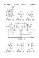
- FIG. 4is a cross-sectional view of memory cell 40 that is coupled to a current limiting circuit 70, It should be noted that the same reference numbers are used in the figures to denote the same elements.
- a semiconductor region 64is an isolation region that is disposed in substrate 62 and separates memory cell 40 from substrate 62.
- Another semiconductor region 66includes memory cell 40 and is disposed in semiconductor region 64.
- Well terminal 61contacts semiconductor region 66.
- substrate 62is a P-type semiconductor material
- semiconductor region 64is an isolated N-well region
- semiconductor region 66is an isolated P-well region.
- N-well and P-well regionsare formed with lighter impurity concentrations when compared with the impurity concentrations used to form the source and drain regions of a MOSFET.
- Memory cell 40 in semiconductor region 66has gate structures 46 and 56 formed thereon.
- gate structures 46 and 56are connected to respective gate terminals 44 and 54.
- Memory cell 40includes control transistor 42 and select transistor 52.
- Control transistor 42has gate terminal 44, gate structure 46, drain region 48, and source region 50.
- Select transistor 52has gate terminal 54, gate structure 56, drain region 50, and source region 58.
- Drain region 48 of control transistor 42is connected to the signal, BIT LINE.
- the source region of control transistor 42is commonly connected to the drain region of select transistor 52 and is referred to by the reference number 50.
- Source region 58 of select transistor 52is connected to power supply conductor 60.
- Current limiting circuit 70includes a power supply conductor 72, a control terminal 74, and an output terminal 76. Output terminal 76 is connected to semiconductor region 64 by an ohmic connection. Current limiting circuit 70 provides a current conduction path between the power supply conductor 72 and the output terminal 76.
- FIG. 5is a preferred embodiment of current limiting circuit 70.
- Current limiting circuit 70is a P-channel MOSFET 80 having a gate terminal, a drain terminal, and a source terminal.
- a MOSFETcan have terminals referred to as a control terminal and current conducting terminals.
- the gate terminal of MOSFET 80serves as control terminal 74 of current limiting circuit 70.
- the source terminal of MOSFET 80serves as power supply conductor 72 of current limiting circuit 70.
- the drain terminal of MOSFET 80serves as output terminal 76 of current limiting circuit 70.
- MOSFET 80As an enhancement transistor is in a conductive mode.
- output terminal 76 of MOSFET 80has a voltage value of about VDD when power supply conductor 72 is supplied with a voltage of VDD.
- Current limiting circuit 70operates in the conductive mode to supply the leakage currents of the reverse-biased diodes that are formed by semiconductor region 64 with substrate 62 and semiconductor region 64 with semiconductor region 66.
- MOSFET 80When control terminal 74 is supplied with a logic one value, i.e., a voltage value of about VDD, MOSFET 80 is in a non-conductive mode of operation. In the non-conductive mode MOSFET 80 is off and operates to block the supply of leakage currents to the reverse-biased diodes that are formed by semiconductor region 64 with substrate 62 and semiconductor region 64 with semiconductor region 66. It should be understood that when MOSFET 80 is non-conductive that another semiconductor device (not shown) can be used to insure that well region 64 is not negatively biased such that the diode formed by region 64 with substrate 62 becomes forward biased.
- FIG. 6is a first alternate embodiment of current limiting circuit 70.
- Current limiting circuit 70is a P-channel MOSFET 82 having a gate terminal, a drain terminal, and a source terminal.
- the gate terminal of MOSFET 82is connected to a power supply conductor and receives a voltage such as, for example, ground.
- the source terminal of MOSFET 82serves as power supply conductor 72 of current limiting circuit 70.
- the drain terminal of MOSFET 82serves as output terminal 76 of current limiting circuit 70.
- the control terminal 74 of current limiting circuit 70is not connected.
- MOSFET 82has an output voltage value at terminal 76 of about VDD when power supply conductor 72 is supplied with a voltage of VDD. MOSFET 82 operates in a conductive mode to supply the leakage currents of the reverse-biased diodes that are formed by semiconductor region 64 with substrate 62 and semiconductor region 64 with semiconductor region 66.
- FIG. 7is a second alternate embodiment of current limiting circuit 70.
- Current limiting circuit 70is an N-channel MOSFET 84 having a gate terminal, a drain terminal, and a source terminal.
- the gate terminal of MOSFET 84serves as control terminal 74 of current limiting circuit 70.
- the source terminal of MOSFET 84serves as output terminal 76 of current limiting circuit 70.
- the drain terminal of MOSFET 84serves as power supply conductor 72 of current limiting circuit 70.
- MOSFET 84As an enhancement transistor is in a conductive mode.
- output terminal 76 of MOSFET 84has a voltage value of VDD minus a threshold voltage value of MOSFET 84 when power supply conductor 72 is supplied with a voltage of VDD.
- MOSFET 84operates in the conductive mode to supply current to the reverse-biased diodes that are formed by semiconductor region 64 with substrate 62 and semiconductor region 64 with semiconductor region 66. In other words, the diode leakage currents are supplied by MOSFET 84.
- MOSFET 84When control terminal 74 is supplied with a logic zero value, i.e., a voltage value of about ground, MOSFET 84 is in a non-conductive mode. In the non-conductive mode MOSFET 84 is off and operates to block the supply of leakage currents to the reverse-biased diodes that are formed by semiconductor region 64 with substrate 62 and semiconductor region 64 with semiconductor region 66.
- FIG. 8is a third alternate embodiment of current limiting circuit 70.
- Current limiting circuit 70is an N-channel MOSFET 86 having a gate terminal, a drain terminal, and a source terminal.
- the commonly connected gate terminal and drain terminal of MOSFET 86serve as power supply conductor 72 of current limiting circuit 70.
- the source terminal of MOSFET 86serves as output terminal 76 of current limiting circuit 70.
- the control terminal 74 of current limiting circuit 70is not connected.
- MOSFET 86has a voltage value at output terminal 76 of VDD minus a threshold voltage value of MOSFET 86 when power supply conductor 72 is supplied with a voltage of VDD. MOSFET 86 operates in a conductive mode to supply the leakage currents of the reverse-biased diodes that are formed by semiconductor region 64 with substrate 62 and semiconductor region 64 with semiconductor region 66.
- FIG. 9is a fourth alternate embodiment of current limiting circuit 70.
- Current limiting circuit 70is a PN-junction diode 88 having an anode and a cathode.
- the anodeis connected to power supply conductor 72 of current limiting circuit 70.
- the cathodeis connected to output terminal 76 of current limiting circuit 70.
- the control terminal 74 of current limiting circuit 70is not connected.
- diode 88has a voltage value at output terminal 76 of VDD minus the voltage of the forward biased diode when power supply conductor 72 is supplied with a voltage of VDD.
- Diode 88operates to supply the leakage currents of the reverse-biased diodes that are formed by semiconductor region 64 with substrate 62 and semiconductor region 64 with semiconductor region 66.
- current limiting circuit 70represent a single device or a plurality of MOSFET devices.
- the memory array of memory circuit 24it is common practice for the memory array of memory circuit 24 to be organized into several sections or banks, such that each bank has reverse-biased diodes formed by semiconductor region 64 with substrate 62 and semiconductor region 64 with semiconductor region 66.
- a plurality of current limiting circuits 70 having commonly connected gate terminalscan be used to limit the leakage currents of the reverse-biased diodes in each bank of the memory array.
- the P-channel MOSFET 80has a gate structure connected to control terminal 74 that includes a width W and a length L.
- the gate of MOSFET 80can be sized to have a width W of about 1.0 micrometers and a length L of about 0.4 micrometers.
- control terminal 74is supplied with a voltage of about zero volts, MOSFET 80 is in the conductive mode and supplies a current of about 25 microamps.
- MOSFET 80is in the non-conductive mode and limits the leakage current to the reverse-biased diodes of each bank to a current of about 1.0 nanoamp.
Landscapes
- Engineering & Computer Science (AREA)
- Microelectronics & Electronic Packaging (AREA)
- Computer Hardware Design (AREA)
- Semiconductor Integrated Circuits (AREA)
- Semiconductor Memories (AREA)
- Non-Volatile Memory (AREA)
- Read Only Memory (AREA)
- Static Random-Access Memory (AREA)
- Power Sources (AREA)
Abstract
Description
______________________________________ CON- TROL BIT TER- LINE MINAL SELECT SOURCE WELL SIG- VOLT- GATE TERMINAL TERMINALMODE NAL AGE VOLTAGE VOLTAGE VOLTAGE______________________________________READ output +1.2 V 0 V/VDD 0 V 0 VPRO- +5.5 V -9 V X 0 V 0 VGRAMERASE floats +13 V 0 V -5 V -5 V______________________________________
Claims (19)
Priority Applications (6)
| Application Number | Priority Date | Filing Date | Title |
|---|---|---|---|
| US08/859,897US5898633A (en) | 1997-05-21 | 1997-05-21 | Circuit and method of limiting leakage current in a memory circuit |
| SG1998001013ASG65067A1 (en) | 1997-05-21 | 1998-05-08 | Circuit and method of limiting leakage current in memory circuit |
| JP14650598AJP4880103B2 (en) | 1997-05-21 | 1998-05-12 | Memory circuit in which supply of leakage current is blocked, radio apparatus including the memory circuit, and leakage current limiting method |
| TW087107825ATW374270B (en) | 1997-05-21 | 1998-05-20 | Circuit and method of limiting leakage current in a memory circuit |
| KR1019980018083AKR100548973B1 (en) | 1997-05-21 | 1998-05-20 | Circuit and method of limiting current in a memory circuit |
| JP2009289022AJP5114470B2 (en) | 1997-05-21 | 2009-12-21 | Circuit and method for limiting leakage current in a memory circuit |
Applications Claiming Priority (1)
| Application Number | Priority Date | Filing Date | Title |
|---|---|---|---|
| US08/859,897US5898633A (en) | 1997-05-21 | 1997-05-21 | Circuit and method of limiting leakage current in a memory circuit |
Publications (1)
| Publication Number | Publication Date |
|---|---|
| US5898633Atrue US5898633A (en) | 1999-04-27 |
Family
ID=25331997
Family Applications (1)
| Application Number | Title | Priority Date | Filing Date |
|---|---|---|---|
| US08/859,897Expired - LifetimeUS5898633A (en) | 1997-05-21 | 1997-05-21 | Circuit and method of limiting leakage current in a memory circuit |
Country Status (5)
| Country | Link |
|---|---|
| US (1) | US5898633A (en) |
| JP (2) | JP4880103B2 (en) |
| KR (1) | KR100548973B1 (en) |
| SG (1) | SG65067A1 (en) |
| TW (1) | TW374270B (en) |
Cited By (3)
| Publication number | Priority date | Publication date | Assignee | Title |
|---|---|---|---|---|
| US6493262B1 (en) | 1998-05-22 | 2002-12-10 | Winbond Electronics Corporation | Method for operating nonvolatile memory cells |
| US20040042318A1 (en)* | 2002-08-29 | 2004-03-04 | Porter Stephen R. | Current limiting antifuse programming path |
| US20060091898A1 (en)* | 2004-03-15 | 2006-05-04 | Rainer Gaggl | Unknown |
Families Citing this family (1)
| Publication number | Priority date | Publication date | Assignee | Title |
|---|---|---|---|---|
| KR100649834B1 (en) | 2004-10-22 | 2006-11-28 | 주식회사 하이닉스반도체 | Leakage Current Control Device for Semiconductor Memory Devices |
Citations (4)
| Publication number | Priority date | Publication date | Assignee | Title |
|---|---|---|---|---|
| US4903093A (en)* | 1987-06-05 | 1990-02-20 | Hitachi, Ltd. | Semiconductor integrated circuit device double isolated CMOS input protection resistor |
| US5497023A (en)* | 1985-09-25 | 1996-03-05 | Hitachi, Ltd. | Semiconductor memory device having separately biased wells for isolation |
| US5557568A (en)* | 1993-03-31 | 1996-09-17 | Kabushiki Kaisha Toshiba | Non-volatile semiconductor memory device with verify mode for verifying data written to memory cells |
| US5640002A (en)* | 1995-08-15 | 1997-06-17 | Ruppert; Jonathan Paul | Portable RF ID tag and barcode reader |
Family Cites Families (15)
| Publication number | Priority date | Publication date | Assignee | Title |
|---|---|---|---|---|
| JPH04229655A (en)* | 1990-06-26 | 1992-08-19 | Mitsubishi Electric Corp | Erasure system at nonvolatile semiconductor memory device |
| JPH04348564A (en)* | 1991-05-27 | 1992-12-03 | Matsushita Electron Corp | Cmos substrate potential supply circuit |
| JPH05205488A (en)* | 1992-01-27 | 1993-08-13 | Fujitsu Ltd | Nonvolatile semiconductor storage device |
| JPH06237164A (en)* | 1993-02-10 | 1994-08-23 | Hitachi Ltd | Semiconductor integrated circuit having power reduction mechanism and electronic device using same |
| JPH0621443A (en)* | 1992-04-17 | 1994-01-28 | Nec Corp | Semiconductor integrated circuit |
| JPH06216346A (en)* | 1992-11-30 | 1994-08-05 | Sony Corp | Semiconductor device |
| JP3520532B2 (en)* | 1993-08-06 | 2004-04-19 | ソニー株式会社 | Driving method of NAND nonvolatile memory |
| JPH0863985A (en)* | 1994-08-29 | 1996-03-08 | Mitsubishi Denki Semiconductor Software Kk | Nonvolatile semiconductor memory device |
| JPH08191954A (en)* | 1995-01-13 | 1996-07-30 | Nippon Denki Ido Tsushin Kk | Game system |
| TW306001B (en)* | 1995-02-08 | 1997-05-21 | Matsushita Electric Industrial Co Ltd | |
| JP3641511B2 (en)* | 1995-06-16 | 2005-04-20 | 株式会社ルネサステクノロジ | Semiconductor device |
| JP3204602B2 (en)* | 1995-07-13 | 2001-09-04 | 株式会社東芝 | Nonvolatile semiconductor memory device |
| JP3606397B2 (en)* | 1995-07-13 | 2005-01-05 | 富士通株式会社 | Mobile phone |
| JP3602216B2 (en)* | 1995-09-19 | 2004-12-15 | 富士通株式会社 | Semiconductor device |
| DE69731170T2 (en)* | 1996-12-13 | 2006-02-02 | Texas Instruments Inc., Dallas | Improvements to or with respect to semiconductor devices |
- 1997
- 1997-05-21USUS08/859,897patent/US5898633A/ennot_activeExpired - Lifetime
- 1998
- 1998-05-08SGSG1998001013Apatent/SG65067A1/enunknown
- 1998-05-12JPJP14650598Apatent/JP4880103B2/ennot_activeExpired - Lifetime
- 1998-05-20KRKR1019980018083Apatent/KR100548973B1/ennot_activeExpired - Lifetime
- 1998-05-20TWTW087107825Apatent/TW374270B/ennot_activeIP Right Cessation
- 2009
- 2009-12-21JPJP2009289022Apatent/JP5114470B2/ennot_activeExpired - Lifetime
Patent Citations (4)
| Publication number | Priority date | Publication date | Assignee | Title |
|---|---|---|---|---|
| US5497023A (en)* | 1985-09-25 | 1996-03-05 | Hitachi, Ltd. | Semiconductor memory device having separately biased wells for isolation |
| US4903093A (en)* | 1987-06-05 | 1990-02-20 | Hitachi, Ltd. | Semiconductor integrated circuit device double isolated CMOS input protection resistor |
| US5557568A (en)* | 1993-03-31 | 1996-09-17 | Kabushiki Kaisha Toshiba | Non-volatile semiconductor memory device with verify mode for verifying data written to memory cells |
| US5640002A (en)* | 1995-08-15 | 1997-06-17 | Ruppert; Jonathan Paul | Portable RF ID tag and barcode reader |
Cited By (12)
| Publication number | Priority date | Publication date | Assignee | Title |
|---|---|---|---|---|
| US6493262B1 (en) | 1998-05-22 | 2002-12-10 | Winbond Electronics Corporation | Method for operating nonvolatile memory cells |
| US20030071301A1 (en)* | 1998-05-22 | 2003-04-17 | Winbond Electronics Corporation | Method for erasing a nonvolatile memory cell formed in a body region of a substrate |
| US20040042318A1 (en)* | 2002-08-29 | 2004-03-04 | Porter Stephen R. | Current limiting antifuse programming path |
| US20050026336A1 (en)* | 2002-08-29 | 2005-02-03 | Porter Stephen R. | Current limiting antifuse programming path |
| US20050024973A1 (en)* | 2002-08-29 | 2005-02-03 | Porter Stephen R. | Current limiting antifuse programming path |
| US6859408B2 (en)* | 2002-08-29 | 2005-02-22 | Micron Technology, Inc. | Current limiting antifuse programming path |
| US20050041508A1 (en)* | 2002-08-29 | 2005-02-24 | Porter Stephen R. | Current limiting antifuse programming path |
| US7091067B2 (en) | 2002-08-29 | 2006-08-15 | Micron Technology, Inc. | Current limiting antifuse programming path |
| US7173855B2 (en) | 2002-08-29 | 2007-02-06 | Micron Technology, Inc. | Current limiting antifuse programming path |
| US7466618B2 (en) | 2002-08-29 | 2008-12-16 | Micron Technology, Inc. | Current limiting antifuse programming path |
| US20060091898A1 (en)* | 2004-03-15 | 2006-05-04 | Rainer Gaggl | Unknown |
| US7295021B2 (en)* | 2004-03-15 | 2007-11-13 | T.I.P.S. Messtechnik Gmbh | Process and circuit for protection of test contacts in high current measurement of semiconductor components |
Also Published As
| Publication number | Publication date |
|---|---|
| JP4880103B2 (en) | 2012-02-22 |
| SG65067A1 (en) | 1999-05-25 |
| JP2010113797A (en) | 2010-05-20 |
| KR100548973B1 (en) | 2006-04-17 |
| KR19980087201A (en) | 1998-12-05 |
| TW374270B (en) | 1999-11-11 |
| JP5114470B2 (en) | 2013-01-09 |
| JPH10335583A (en) | 1998-12-18 |
Similar Documents
| Publication | Publication Date | Title |
|---|---|---|
| KR102121075B1 (en) | Body-biased switching device | |
| US6977519B2 (en) | Digital logic with reduced leakage | |
| EP0280236B1 (en) | Method of manufacturing an insulated-gate semicustom integrated circuit | |
| US5760652A (en) | Integrated circuit device | |
| US5898235A (en) | Integrated circuit with power dissipation control | |
| US8847672B2 (en) | Switching device with resistive divider | |
| EP0480201A1 (en) | Off-chip drivers | |
| US20070102730A1 (en) | Switching circuit and semicondcutor device | |
| EP0199305A2 (en) | Programmable read only memory operable with reduced programming power consumption | |
| US4893275A (en) | High voltage switching circuit in a nonvolatile memory | |
| US8977217B1 (en) | Switching device with negative bias circuit | |
| US20250022674A1 (en) | Devices and methods for programming a fuse | |
| JPS60192418A (en) | High speed input buffer | |
| JP5114470B2 (en) | Circuit and method for limiting leakage current in a memory circuit | |
| US5754010A (en) | Memory circuit and method for sensing data | |
| US20040266092A1 (en) | System and method for data retention with reduced leakage current | |
| KR850006784A (en) | Semiconductor integrated circuit device | |
| KR20030051351A (en) | Semiconductor integrated circuit | |
| US8923782B1 (en) | Switching device with diode-biased field-effect transistor (FET) | |
| US6041221A (en) | Circuit and method for verifying data of a wireless communications device | |
| US6049498A (en) | Double transistor switch for supplying multiple voltages to flash memory wordlines | |
| JP2002500400A (en) | Active transponder that can be switched to a passive transponder | |
| US5892379A (en) | Transistor protection circuit and method | |
| US6798252B2 (en) | High speed sense amplifier | |
| US5689197A (en) | BIMOS-type current switch apparatus |
Legal Events
| Date | Code | Title | Description |
|---|---|---|---|
| AS | Assignment | Owner name:MOTOROLA, INC., ILLINOIS Free format text:ASSIGNMENT OF ASSIGNORS INTEREST;ASSIGNORS:CARAVELLA, JAMES S.;MIETUS, DAVID F.;MOORE, JEREMY W.;REEL/FRAME:008575/0722 Effective date:19970430 | |
| STCF | Information on status: patent grant | Free format text:PATENTED CASE | |
| CC | Certificate of correction | ||
| FPAY | Fee payment | Year of fee payment:4 | |
| AS | Assignment | Owner name:FREESCALE SEMICONDUCTOR, INC., TEXAS Free format text:ASSIGNMENT OF ASSIGNORS INTEREST;ASSIGNOR:MOTOROLA, INC.;REEL/FRAME:015698/0657 Effective date:20040404 Owner name:FREESCALE SEMICONDUCTOR, INC.,TEXAS Free format text:ASSIGNMENT OF ASSIGNORS INTEREST;ASSIGNOR:MOTOROLA, INC.;REEL/FRAME:015698/0657 Effective date:20040404 | |
| FPAY | Fee payment | Year of fee payment:8 | |
| AS | Assignment | Owner name:CITIBANK, N.A. AS COLLATERAL AGENT, NEW YORK Free format text:SECURITY AGREEMENT;ASSIGNORS:FREESCALE SEMICONDUCTOR, INC.;FREESCALE ACQUISITION CORPORATION;FREESCALE ACQUISITION HOLDINGS CORP.;AND OTHERS;REEL/FRAME:018855/0129 Effective date:20061201 Owner name:CITIBANK, N.A. AS COLLATERAL AGENT,NEW YORK Free format text:SECURITY AGREEMENT;ASSIGNORS:FREESCALE SEMICONDUCTOR, INC.;FREESCALE ACQUISITION CORPORATION;FREESCALE ACQUISITION HOLDINGS CORP.;AND OTHERS;REEL/FRAME:018855/0129 Effective date:20061201 | |
| AS | Assignment | Owner name:CITIBANK, N.A., AS COLLATERAL AGENT,NEW YORK Free format text:SECURITY AGREEMENT;ASSIGNOR:FREESCALE SEMICONDUCTOR, INC.;REEL/FRAME:024397/0001 Effective date:20100413 Owner name:CITIBANK, N.A., AS COLLATERAL AGENT, NEW YORK Free format text:SECURITY AGREEMENT;ASSIGNOR:FREESCALE SEMICONDUCTOR, INC.;REEL/FRAME:024397/0001 Effective date:20100413 | |
| FPAY | Fee payment | Year of fee payment:12 | |
| AS | Assignment | Owner name:CITIBANK, N.A., AS NOTES COLLATERAL AGENT, NEW YORK Free format text:SECURITY AGREEMENT;ASSIGNOR:FREESCALE SEMICONDUCTOR, INC.;REEL/FRAME:030633/0424 Effective date:20130521 Owner name:CITIBANK, N.A., AS NOTES COLLATERAL AGENT, NEW YOR Free format text:SECURITY AGREEMENT;ASSIGNOR:FREESCALE SEMICONDUCTOR, INC.;REEL/FRAME:030633/0424 Effective date:20130521 | |
| AS | Assignment | Owner name:CITIBANK, N.A., AS NOTES COLLATERAL AGENT, NEW YORK Free format text:SECURITY AGREEMENT;ASSIGNOR:FREESCALE SEMICONDUCTOR, INC.;REEL/FRAME:031591/0266 Effective date:20131101 Owner name:CITIBANK, N.A., AS NOTES COLLATERAL AGENT, NEW YOR Free format text:SECURITY AGREEMENT;ASSIGNOR:FREESCALE SEMICONDUCTOR, INC.;REEL/FRAME:031591/0266 Effective date:20131101 | |
| AS | Assignment | Owner name:FREESCALE SEMICONDUCTOR, INC., TEXAS Free format text:PATENT RELEASE;ASSIGNOR:CITIBANK, N.A., AS COLLATERAL AGENT;REEL/FRAME:037354/0225 Effective date:20151207 Owner name:FREESCALE SEMICONDUCTOR, INC., TEXAS Free format text:PATENT RELEASE;ASSIGNOR:CITIBANK, N.A., AS COLLATERAL AGENT;REEL/FRAME:037356/0143 Effective date:20151207 Owner name:FREESCALE SEMICONDUCTOR, INC., TEXAS Free format text:PATENT RELEASE;ASSIGNOR:CITIBANK, N.A., AS COLLATERAL AGENT;REEL/FRAME:037356/0553 Effective date:20151207 | |
| AS | Assignment | Owner name:MORGAN STANLEY SENIOR FUNDING, INC., MARYLAND Free format text:ASSIGNMENT AND ASSUMPTION OF SECURITY INTEREST IN PATENTS;ASSIGNOR:CITIBANK, N.A.;REEL/FRAME:037486/0517 Effective date:20151207 | |
| AS | Assignment | Owner name:MORGAN STANLEY SENIOR FUNDING, INC., MARYLAND Free format text:ASSIGNMENT AND ASSUMPTION OF SECURITY INTEREST IN PATENTS;ASSIGNOR:CITIBANK, N.A.;REEL/FRAME:037518/0292 Effective date:20151207 | |
| AS | Assignment | Owner name:MORGAN STANLEY SENIOR FUNDING, INC., MARYLAND Free format text:SUPPLEMENT TO THE SECURITY AGREEMENT;ASSIGNOR:FREESCALE SEMICONDUCTOR, INC.;REEL/FRAME:039138/0001 Effective date:20160525 | |
| AS | Assignment | Owner name:NXP, B.V., F/K/A FREESCALE SEMICONDUCTOR, INC., NETHERLANDS Free format text:RELEASE BY SECURED PARTY;ASSIGNOR:MORGAN STANLEY SENIOR FUNDING, INC.;REEL/FRAME:040925/0001 Effective date:20160912 Owner name:NXP, B.V., F/K/A FREESCALE SEMICONDUCTOR, INC., NE Free format text:RELEASE BY SECURED PARTY;ASSIGNOR:MORGAN STANLEY SENIOR FUNDING, INC.;REEL/FRAME:040925/0001 Effective date:20160912 | |
| AS | Assignment | Owner name:NXP B.V., NETHERLANDS Free format text:RELEASE BY SECURED PARTY;ASSIGNOR:MORGAN STANLEY SENIOR FUNDING, INC.;REEL/FRAME:040928/0001 Effective date:20160622 | |
| AS | Assignment | Owner name:NXP USA, INC., TEXAS Free format text:CHANGE OF NAME;ASSIGNOR:FREESCALE SEMICONDUCTOR, INC.;REEL/FRAME:040652/0241 Effective date:20161107 Owner name:NXP USA, INC., TEXAS Free format text:MERGER;ASSIGNOR:FREESCALE SEMICONDUCTOR, INC.;REEL/FRAME:040652/0241 Effective date:20161107 | |
| AS | Assignment | Owner name:NXP USA, INC., TEXAS Free format text:CORRECTIVE ASSIGNMENT TO CORRECT THE NATURE OF CONVEYANCE PREVIOUSLY RECORDED AT REEL: 040652 FRAME: 0241. ASSIGNOR(S) HEREBY CONFIRMS THE MERGER AND CHANGE OF NAME;ASSIGNOR:FREESCALE SEMICONDUCTOR, INC.;REEL/FRAME:041260/0850 Effective date:20161107 | |
| AS | Assignment | Owner name:MORGAN STANLEY SENIOR FUNDING, INC., MARYLAND Free format text:CORRECTIVE ASSIGNMENT TO CORRECT THE REMOVE PATENTS 8108266 AND 8062324 AND REPLACE THEM WITH 6108266 AND 8060324 PREVIOUSLY RECORDED ON REEL 037518 FRAME 0292. ASSIGNOR(S) HEREBY CONFIRMS THE ASSIGNMENT AND ASSUMPTION OF SECURITY INTEREST IN PATENTS;ASSIGNOR:CITIBANK, N.A.;REEL/FRAME:041703/0536 Effective date:20151207 | |
| AS | Assignment | Owner name:SHENZHEN XINGUODU TECHNOLOGY CO., LTD., CHINA Free format text:CORRECTIVE ASSIGNMENT TO CORRECT THE TO CORRECT THE APPLICATION NO. FROM 13,883,290 TO 13,833,290 PREVIOUSLY RECORDED ON REEL 041703 FRAME 0536. ASSIGNOR(S) HEREBY CONFIRMS THE THE ASSIGNMENT AND ASSUMPTION OF SECURITYINTEREST IN PATENTS.;ASSIGNOR:MORGAN STANLEY SENIOR FUNDING, INC.;REEL/FRAME:048734/0001 Effective date:20190217 | |
| AS | Assignment | Owner name:NXP B.V., NETHERLANDS Free format text:RELEASE BY SECURED PARTY;ASSIGNOR:MORGAN STANLEY SENIOR FUNDING, INC.;REEL/FRAME:050744/0097 Effective date:20190903 | |
| AS | Assignment | Owner name:MORGAN STANLEY SENIOR FUNDING, INC., MARYLAND Free format text:CORRECTIVE ASSIGNMENT TO CORRECT THE REMOVE APPLICATION11759915 AND REPLACE IT WITH APPLICATION 11759935 PREVIOUSLY RECORDED ON REEL 037486 FRAME 0517. ASSIGNOR(S) HEREBY CONFIRMS THE ASSIGNMENT AND ASSUMPTION OF SECURITYINTEREST IN PATENTS;ASSIGNOR:CITIBANK, N.A.;REEL/FRAME:053547/0421 Effective date:20151207 | |
| AS | Assignment | Owner name:NXP B.V., NETHERLANDS Free format text:CORRECTIVE ASSIGNMENT TO CORRECT THE REMOVEAPPLICATION 11759915 AND REPLACE IT WITH APPLICATION11759935 PREVIOUSLY RECORDED ON REEL 040928 FRAME 0001. ASSIGNOR(S) HEREBY CONFIRMS THE RELEASE OF SECURITYINTEREST;ASSIGNOR:MORGAN STANLEY SENIOR FUNDING, INC.;REEL/FRAME:052915/0001 Effective date:20160622 | |
| AS | Assignment | Owner name:NXP, B.V. F/K/A FREESCALE SEMICONDUCTOR, INC., NETHERLANDS Free format text:CORRECTIVE ASSIGNMENT TO CORRECT THE REMOVEAPPLICATION 11759915 AND REPLACE IT WITH APPLICATION11759935 PREVIOUSLY RECORDED ON REEL 040925 FRAME 0001. ASSIGNOR(S) HEREBY CONFIRMS THE RELEASE OF SECURITYINTEREST;ASSIGNOR:MORGAN STANLEY SENIOR FUNDING, INC.;REEL/FRAME:052917/0001 Effective date:20160912 |