US5898515A - Light reflecting micromachined cantilever - Google Patents
Light reflecting micromachined cantileverDownload PDFInfo
- Publication number
- US5898515A US5898515AUS08/752,134US75213496AUS5898515AUS 5898515 AUS5898515 AUS 5898515AUS 75213496 AUS75213496 AUS 75213496AUS 5898515 AUS5898515 AUS 5898515A
- Authority
- US
- United States
- Prior art keywords
- cantilever member
- support body
- cantilever
- deflection
- reflector
- Prior art date
- Legal status (The legal status is an assumption and is not a legal conclusion. Google has not performed a legal analysis and makes no representation as to the accuracy of the status listed.)
- Expired - Fee Related
Links
- XUIMIQQOPSSXEZ-UHFFFAOYSA-NSiliconChemical compound[Si]XUIMIQQOPSSXEZ-UHFFFAOYSA-N0.000claimsabstractdescription13
- 230000005855radiationEffects0.000claimsabstractdescription13
- 229910052710siliconInorganic materials0.000claimsabstractdescription13
- 239000010703siliconSubstances0.000claimsabstractdescription13
- 239000000696magnetic materialSubstances0.000claimsdescription22
- 239000012528membraneSubstances0.000claimsdescription5
- 239000000758substrateSubstances0.000description21
- 238000004519manufacturing processMethods0.000description10
- VYPSYNLAJGMNEJ-UHFFFAOYSA-NSilicium dioxideChemical compoundO=[Si]=OVYPSYNLAJGMNEJ-UHFFFAOYSA-N0.000description8
- 238000000034methodMethods0.000description8
- 230000004913activationEffects0.000description5
- 229910052681coesiteInorganic materials0.000description4
- 229910052906cristobaliteInorganic materials0.000description4
- 239000000463materialSubstances0.000description4
- 239000000377silicon dioxideSubstances0.000description4
- 229910052682stishoviteInorganic materials0.000description4
- 229910052905tridymiteInorganic materials0.000description4
- 229910052581Si3N4Inorganic materials0.000description3
- 229910004205SiNXInorganic materials0.000description3
- 238000001312dry etchingMethods0.000description3
- 229920002120photoresistant polymerPolymers0.000description3
- 238000001020plasma etchingMethods0.000description3
- HQVNEWCFYHHQES-UHFFFAOYSA-Nsilicon nitrideChemical compoundN12[Si]34N5[Si]62N3[Si]51N64HQVNEWCFYHHQES-UHFFFAOYSA-N0.000description3
- KRHYYFGTRYWZRS-UHFFFAOYSA-NFluoraneChemical compoundFKRHYYFGTRYWZRS-UHFFFAOYSA-N0.000description2
- 238000005452bendingMethods0.000description2
- GUBSQCSIIDQXLB-UHFFFAOYSA-Ncobalt platinumChemical compound[Co].[Pt].[Pt].[Pt]GUBSQCSIIDQXLB-UHFFFAOYSA-N0.000description2
- 230000000694effectsEffects0.000description2
- 230000004907fluxEffects0.000description2
- 230000010354integrationEffects0.000description2
- 239000010409thin filmSubstances0.000description2
- RYGMFSIKBFXOCR-UHFFFAOYSA-NCopperChemical compound[Cu]RYGMFSIKBFXOCR-UHFFFAOYSA-N0.000description1
- 229910020707Co—PtInorganic materials0.000description1
- 241001061076Melanonus zugmayeriSpecies0.000description1
- 229910002837PtCoInorganic materials0.000description1
- BQCADISMDOOEFD-UHFFFAOYSA-NSilverChemical compound[Ag]BQCADISMDOOEFD-UHFFFAOYSA-N0.000description1
- 229910045601alloyInorganic materials0.000description1
- 239000000956alloySubstances0.000description1
- 229910000828alnicoInorganic materials0.000description1
- 229910052782aluminiumInorganic materials0.000description1
- XAGFODPZIPBFFR-UHFFFAOYSA-NaluminiumChemical compound[Al]XAGFODPZIPBFFR-UHFFFAOYSA-N0.000description1
- 239000004020conductorSubstances0.000description1
- 229910052802copperInorganic materials0.000description1
- 239000010949copperSubstances0.000description1
- 230000005670electromagnetic radiationEffects0.000description1
- 238000005530etchingMethods0.000description1
- PCHJSUWPFVWCPO-UHFFFAOYSA-NgoldChemical compound[Au]PCHJSUWPFVWCPO-UHFFFAOYSA-N0.000description1
- 229910052737goldInorganic materials0.000description1
- 239000010931goldSubstances0.000description1
- 239000011810insulating materialSubstances0.000description1
- 230000003993interactionEffects0.000description1
- 238000001755magnetron sputter depositionMethods0.000description1
- 238000012986modificationMethods0.000description1
- 230000004048modificationEffects0.000description1
- 229910000889permalloyInorganic materials0.000description1
- 238000000623plasma-assisted chemical vapour depositionMethods0.000description1
- 230000010287polarizationEffects0.000description1
- 238000005498polishingMethods0.000description1
- 230000009467reductionEffects0.000description1
- 229910052709silverInorganic materials0.000description1
- 239000004332silverSubstances0.000description1
- 239000000126substanceSubstances0.000description1
Images


Classifications
- G—PHYSICS
- G02—OPTICS
- G02B—OPTICAL ELEMENTS, SYSTEMS OR APPARATUS
- G02B26/00—Optical devices or arrangements for the control of light using movable or deformable optical elements
- G02B26/08—Optical devices or arrangements for the control of light using movable or deformable optical elements for controlling the direction of light
- G02B26/0816—Optical devices or arrangements for the control of light using movable or deformable optical elements for controlling the direction of light by means of one or more reflecting elements
- G02B26/0833—Optical devices or arrangements for the control of light using movable or deformable optical elements for controlling the direction of light by means of one or more reflecting elements the reflecting element being a micromechanical device, e.g. a MEMS mirror, DMD
- G02B26/085—Optical devices or arrangements for the control of light using movable or deformable optical elements for controlling the direction of light by means of one or more reflecting elements the reflecting element being a micromechanical device, e.g. a MEMS mirror, DMD the reflecting means being moved or deformed by electromagnetic means
Definitions
- This inventionrelates generally to the field of radiation reflectors and more particularly to a miniature electromagnetically driven radiation (light) reflector that is fabricated on a silicon substrate.
- the subject of this disclosureis a novel integrated micro-electromagnetic light reflector.
- This reflectorcomprises a cantilever, activation current trace, flux focusing member, and integrated control circuitry to control the current to the activation trace.
- the cantileverfurther comprises a silicon nitride base which is coated with a hard magnetic material that is polarized along its length.
- the magnetic materialis itself coated with a thin metallic layer for reflecting incident light.
- This devicelends itself to automated mass fabrication thereby reducing per unit cost with improved reliability. Moreover, it enables a reduction in size (less than 1 cubic mm) and can be fully integrated with drive electronics etc., all on the same substrate. This makes it ideal for applications such as digital display and printing devices.
- a radiation reflectorcomprised of:
- a cantilever membermounted to said support body for deflection into said recess
- electromagnet meansintegral with said support body for deflecting said cantilever member to reflect incident radiation to a second position by interacting with said poled magnet.
- a miniature electromagnetic light reflector fabricated on a silicon substratecomprises a cantilever, activation current trace, flux focusing member, and integrated control circuitry to control the current to the activation trace.
- the cantileveris formed from a silicon nitride base which is coated with a hard magnetic material that is polarized along its length. The magnetic material is itself coated with a thin metallic layer for reflecting incident light.
- micro-electromagnetic shutterspermits integrated micro-electromagnetic shutters to be manufactured using modern methods of mass integration, thereby substantially reducing assembly cost, and these shutters enable a high degree of miniaturization with improved reliability.
- FIG. 1is perspective representation of a preferred embodiment of the invention
- FIG. 2is a section view of the preferred representation taken along the section line A--A in FIG. 1;
- FIG. 3is a section view illustrating a deflection of the light reflective element
- FIGS. 4A and 4Billustrate in perspective view the structure resulting from a first fabrication step and a section view of the resultant structure taken along the section lines B--B, respectively;
- FIGS. 5A and 5Billustrate in perspective view the structure resulting from a second fabrication step and a section view of the resultant structure taken along the section lines B--B, respectively;
- FIGS. 6A and 6Billustrate in perspective view the structure resulting from a third fabrication step and a section view of the resultant structure taken along the section lines B--B, respectively;
- FIGS. 7A and 7Billustrate in perspective view the structure resulting from a fourth fabrication step and a section view of the resultant structure taken along the section lines B--B, respectively;
- FIGS. 8A and 8Billustrate in perspective view the structure resulting from a fifth fabrication step and a section view of the resultant structure taken along the section lines B--B, respectively;
- FIGS. 9A and 9Billustrate in perspective view the structure resulting from a sixth fabrication step and a section view of the resultant structure taken along the section lines B--B, respectively;
- FIGS. 10A and 10Billustrate in perspective view the structure resulting from a seventh fabrication step and a section view of the resultant structure taken along the section lines B--B, respectively;
- FIGS. 11A and 11Billustrate in perspective view the structure resulting from an eighth fabrication step and a section view of the resultant structure taken along the section lines B--B, respectively;
- FIG. 12illustrates in perspective view a system incorporating an array of light deflectors.
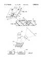
- a perspective view of a reflector 10is shown. Specifically, a cantilever 12 is supported above a cavity 14 formed in silicon substrate 16.
- the cantilever 12comprises a silicon nitride base 18 (shown in FIG. 2) which is coated with a layer of hard magnetic material 20 that is polarized along its length and a reflective layer 22.
- a materialsuch as AlNiCo or PtCo having a magnetic property and a highly reflective property may be substituted for 20 and 22.
- a current trace 24is formed in the substrate 16.
- a soft magnetic material 26is deposited in the substrate adjacent the trace 24.
- a second soft magnetic material 28is deposited in the substrate below the free end of the cantilever 12.
- Drive electronics 30are formed in the substrate 16 to receive input data to which the cantilever is to respond by bending or not bending.
- the drive electronicsmay be left off of the substrate 16 and positioned remote from the reflector 10.
- a power source 32is connected to the reflector 10 to provide the power necessary to drive the cantilever 12 and the integrated drive electronics 30.
- FIG. 2Also shown in FIG. 2 are the incident light rays, IL, and an aperture 70 for eliminating the passage of stray light onto optics 72 which focuses reflected light, RL, onto a display screen 74 when the cantilever is activated as shown in FIG. 3.
- the cantilever 12In operation, referring to FIGS. 2 and 3, the cantilever 12 overhangs the cavity 14 with its free end in proximity to the current trace 24.
- the soft magnetic material 26 residing behind the current trace 24interacts with the magnetic field generated when current flows through the trace.
- the incident light, ILis shown perpendicular to the undeflected cantilever 12. Notice that in the position shown in FIG. 2, no reflected light, RL, passes through the aperture 70 to optics 72.
- the cantilever 12is shown deflected downward due to current being applied to the current trace 24 in the direction (into the paper) indicated by the arrow tails.
- the north pole of the magnetic layer 20 of the cantilever 12experiences a Lorentz force which acts to deflect the cantilever downwards as shown.
- the presence of the soft magnetic material 26enhances the Lorentz force.
- the reflected light, RLpasses through the aperture 70, through the optics 72 onto the display screen 74.
- soft magnetic material 26is not essential to the operation of the reflector 10, but it enhances the performance of the reflector.
- the optional soft magnetic material 28may be placed as shown to interact with the end pole of the magnetic layer 20 on the cantilever 12 to provide a downward detent position for the bent cantilever 12 after the deflection current has been applied to the current trace 24.
- This detent arrangementminimizes the energy needed to hold the cantilever 12 in the downward deflected position.
- an etch mask 40such as photoresist is applied to a silicon substrate 16 and patterned using conventional photolithographic techniques to create a window 42.
- a cavity 14is then formed in the silicon substrate 16 by a dry etching technique such as high density plasma etching.
- the etch mask 40is subsequently removed.
- the cavity 14is refilled with a sacrificial material, for example, low density PECVD SiO 2 .
- the substrate 16is planarized by chemical mechanical polishing.
- an etch mask 44such as a photoresist is applied to the substrate 16 and patterned using conventional photolithographic techniques to create a window 46 shaped like trace 24.
- a trench 48is then etched in the substrate 16 by a dry etching technique such as high density plasma etching. The etch mask 44 is subsequently removed.
- the trench 48is refilled with a conductive material such as copper and planarized.
- a conductive materialsuch as copper and planarized.
- an insulating materialmay be applied to the trench bottom and sidewalls to prevent electrical conduction from the current trace 24 to the silicon substrate 16.
- an etch mask 50such as photoresist is applied to the silicon substrate 16 and patterned using conventional photolithographic techniques to create a window 52 in the shape of the soft magnetic material 26.
- a second trench 54is etched in the silicon substrate 16 by a dry etching technique such as high density plasma etching. The etch mask 50 is subsequently removed.
- the second trench 54is refilled with a soft magnetic material such as permalloy and planarized.
- a layer of membrane material 18such as SiN x is applied to the silicon substrate 16.
- Standard photolithographic and thin film etching techniquesare used to pattern openings in the SiN x so as to create contact openings for the current trace 24 and a partial opening above the SiO 2 -filled cavity.
- a layer of hard magnetic material 20is then formed and poled on top of the SiN x above the cavity.
- the reflective layer 22may be formed on top of the layer of hard magnetic material 20.
- the hard magnetic material 20is preferably made from cobalt-platinum (CoPt) which is deposited for in-plane polarization at room temperature using dc or rf magnetron sputtering as described in the publication entitled “Structure and Micromagnetic Predictions for Hysteretic Phenomena in a Novel Co-Pt Permanent Magnet Thin Film,” by R. H. Victora, et al. in the JOURNAL OF MAGNET AND MAGNETIC MATERIALS, Vol. 97, 1991, pp. 343-352.
- the magnetic material 20is polarized along the length of cantilever 12, and overcoated with a highly reflective layer 22 comprised of gold, silver, aluminum, or alloys thereof.
- the SiO 2is removed by a preferential etchant such as hydrofluoric acid to etch out the SiO 2 located in the cavity 14 below the cantilever 12 to complete the reflector 10.
- a preferential etchantsuch as hydrofluoric acid to etch out the SiO 2 located in the cavity 14 below the cantilever 12 to complete the reflector 10.
- an array 100 of reflectors 10is exposed to I L from a light source 102 via optics 104.
- the incident lightis reflected off of the reflective surface of each of the reflectors 10.
- An image (data) source 106provides digital information to a digital controller 108.
- the digital controller 108has outputs corresponding in number to the number of reflectors 10. Each output is connected to provide a current to the current trace 24 of a respective reflector 10 so as to cause a respective cantilever 12 to either deflect or not according to the image to be formed.
- a deflection of a cantileverwill cause a ray of reflective light RL to be directed to a display screen 74 via optics 72 thus forming a replica of the image from the image source 106 onto the display 74.
Landscapes
- Physics & Mathematics (AREA)
- Electromagnetism (AREA)
- General Physics & Mathematics (AREA)
- Optics & Photonics (AREA)
- Mechanical Light Control Or Optical Switches (AREA)
Abstract
Description
This invention relates generally to the field of radiation reflectors and more particularly to a miniature electromagnetically driven radiation (light) reflector that is fabricated on a silicon substrate.
Conventional electromagnetic radiation (light) reflectors consist of flexible members that move relative to an incident light beam to reflect the incident light at a predefined angle. For magnetically based devices, the movement of the reflector is usually due to the interactions of energized coils with permanent magnets arranged in proximity to one another. These conventional reflectors are relatively large (1 cubic cm) and tend to require labor intensive assembly. The subject of this disclosure is a novel integrated micro-electromagnetic light reflector. This reflector comprises a cantilever, activation current trace, flux focusing member, and integrated control circuitry to control the current to the activation trace. The cantilever further comprises a silicon nitride base which is coated with a hard magnetic material that is polarized along its length. The magnetic material is itself coated with a thin metallic layer for reflecting incident light. This device lends itself to automated mass fabrication thereby reducing per unit cost with improved reliability. Moreover, it enables a reduction in size (less than 1 cubic mm) and can be fully integrated with drive electronics etc., all on the same substrate. This makes it ideal for applications such as digital display and printing devices.
The present invention is directed to overcoming one or more of the problems set forth above. Briefly summarized, according to one aspect of the present invention there is provided a radiation reflector comprised of:
a support body having a recess formed therein;
a cantilever member mounted to said support body for deflection into said recess;
radiation reflection means integral with said cantilever member for reflecting incident radiation to a first position when the cantilever member is not deflected;
a poled magnet mounted on said cantilever member; and
electromagnet means integral with said support body for deflecting said cantilever member to reflect incident radiation to a second position by interacting with said poled magnet.
A miniature electromagnetic light reflector fabricated on a silicon substrate is disclosed. The substrate comprises a cantilever, activation current trace, flux focusing member, and integrated control circuitry to control the current to the activation trace. The cantilever is formed from a silicon nitride base which is coated with a hard magnetic material that is polarized along its length. The magnetic material is itself coated with a thin metallic layer for reflecting incident light.
These and other aspects, objects, features, and advantages of the present invention will be more clearly understood and appreciated from a review of the following detailed description of the preferred embodiments and appended claims, and by reference to the accompanying drawings.
The present invention has the following advantages in that it is:
miniaturized,
low in cost,
amiable to automated manufacturing, and
permits integrated micro-electromagnetic shutters to be manufactured using modern methods of mass integration, thereby substantially reducing assembly cost, and these shutters enable a high degree of miniaturization with improved reliability.
FIG. 1 is perspective representation of a preferred embodiment of the invention;
FIG. 2 is a section view of the preferred representation taken along the section line A--A in FIG. 1;
FIG. 3 is a section view illustrating a deflection of the light reflective element;
FIGS. 4A and 4B illustrate in perspective view the structure resulting from a first fabrication step and a section view of the resultant structure taken along the section lines B--B, respectively;
FIGS. 5A and 5B illustrate in perspective view the structure resulting from a second fabrication step and a section view of the resultant structure taken along the section lines B--B, respectively;
FIGS. 6A and 6B illustrate in perspective view the structure resulting from a third fabrication step and a section view of the resultant structure taken along the section lines B--B, respectively;
FIGS. 7A and 7B illustrate in perspective view the structure resulting from a fourth fabrication step and a section view of the resultant structure taken along the section lines B--B, respectively;
FIGS. 8A and 8B illustrate in perspective view the structure resulting from a fifth fabrication step and a section view of the resultant structure taken along the section lines B--B, respectively;
FIGS. 9A and 9B illustrate in perspective view the structure resulting from a sixth fabrication step and a section view of the resultant structure taken along the section lines B--B, respectively;
FIGS. 10A and 10B illustrate in perspective view the structure resulting from a seventh fabrication step and a section view of the resultant structure taken along the section lines B--B, respectively;
FIGS. 11A and 11B illustrate in perspective view the structure resulting from an eighth fabrication step and a section view of the resultant structure taken along the section lines B--B, respectively; and
FIG. 12 illustrates in perspective view a system incorporating an array of light deflectors.
To facilitate understanding, identical reference numerals have been used, where possible, to designate identical elements that are common to the figures.
Referring to FIGS. 1 and 2, a perspective view of areflector 10 is shown. Specifically, acantilever 12 is supported above acavity 14 formed insilicon substrate 16. Thecantilever 12 comprises a silicon nitride base 18 (shown in FIG. 2) which is coated with a layer of hardmagnetic material 20 that is polarized along its length and areflective layer 22. A material such as AlNiCo or PtCo having a magnetic property and a highly reflective property may be substituted for 20 and 22. Acurrent trace 24 is formed in thesubstrate 16. A softmagnetic material 26 is deposited in the substrate adjacent thetrace 24. Optionally, a second softmagnetic material 28 is deposited in the substrate below the free end of thecantilever 12. Driveelectronics 30 are formed in thesubstrate 16 to receive input data to which the cantilever is to respond by bending or not bending. Optionally, the drive electronics may be left off of thesubstrate 16 and positioned remote from thereflector 10. For maximum integration effect it is preferable to integrate thedrive electronics 30 into thesubstrate 16. Apower source 32 is connected to thereflector 10 to provide the power necessary to drive thecantilever 12 and theintegrated drive electronics 30. Also shown in FIG. 2 are the incident light rays, IL, and anaperture 70 for eliminating the passage of stray light ontooptics 72 which focuses reflected light, RL, onto adisplay screen 74 when the cantilever is activated as shown in FIG. 3.
In operation, referring to FIGS. 2 and 3, thecantilever 12 overhangs thecavity 14 with its free end in proximity to thecurrent trace 24. The softmagnetic material 26 residing behind thecurrent trace 24 interacts with the magnetic field generated when current flows through the trace. For the purpose of illustration, the incident light, IL, is shown perpendicular to theundeflected cantilever 12. Notice that in the position shown in FIG. 2, no reflected light, RL, passes through theaperture 70 tooptics 72. Specifically in FIG. 3, thecantilever 12 is shown deflected downward due to current being applied to thecurrent trace 24 in the direction (into the paper) indicated by the arrow tails. More specifically, as current flows through the activation trace (into the paper), the north pole of themagnetic layer 20 of thecantilever 12 experiences a Lorentz force which acts to deflect the cantilever downwards as shown. The presence of the softmagnetic material 26 enhances the Lorentz force. In this position, the reflected light, RL, passes through theaperture 70, through theoptics 72 onto thedisplay screen 74. Thus one can control the light output to a given surface over a small spot (pixel) and this can be adapted to digital display and printing applications. It is instructive to note that softmagnetic material 26 is not essential to the operation of thereflector 10, but it enhances the performance of the reflector.
As previously mentioned, the optional softmagnetic material 28 may be placed as shown to interact with the end pole of themagnetic layer 20 on thecantilever 12 to provide a downward detent position for thebent cantilever 12 after the deflection current has been applied to thecurrent trace 24. This detent arrangement minimizes the energy needed to hold thecantilever 12 in the downward deflected position.
Referring to FIGS. 4A and 4B, anetch mask 40 such as photoresist is applied to asilicon substrate 16 and patterned using conventional photolithographic techniques to create awindow 42. Acavity 14 is then formed in thesilicon substrate 16 by a dry etching technique such as high density plasma etching. Theetch mask 40 is subsequently removed.
Referring to FIGS. 5A and 5B, thecavity 14 is refilled with a sacrificial material, for example, low density PECVD SiO2. Thesubstrate 16 is planarized by chemical mechanical polishing.
Referring to FIGS. 6A and 6B, anetch mask 44 such as a photoresist is applied to thesubstrate 16 and patterned using conventional photolithographic techniques to create awindow 46 shaped liketrace 24. Atrench 48 is then etched in thesubstrate 16 by a dry etching technique such as high density plasma etching. Theetch mask 44 is subsequently removed.
Referring to FIGS. 7A and 7B, thetrench 48 is refilled with a conductive material such as copper and planarized. Optionally, an insulating material may be applied to the trench bottom and sidewalls to prevent electrical conduction from thecurrent trace 24 to thesilicon substrate 16.
Referring to FIGS. 8A and 8B, anetch mask 50 such as photoresist is applied to thesilicon substrate 16 and patterned using conventional photolithographic techniques to create awindow 52 in the shape of the softmagnetic material 26. Asecond trench 54 is etched in thesilicon substrate 16 by a dry etching technique such as high density plasma etching. Theetch mask 50 is subsequently removed.
Referring to FIGS. 9A and 9B, thesecond trench 54 is refilled with a soft magnetic material such as permalloy and planarized.
Referring to FIGS. 10A and 10B, a layer ofmembrane material 18 such as SiNx is applied to thesilicon substrate 16. Standard photolithographic and thin film etching techniques are used to pattern openings in the SiNx so as to create contact openings for thecurrent trace 24 and a partial opening above the SiO2 -filled cavity. A layer of hardmagnetic material 20 is then formed and poled on top of the SiNx above the cavity. Next, thereflective layer 22 may be formed on top of the layer of hardmagnetic material 20.
The hardmagnetic material 20 is preferably made from cobalt-platinum (CoPt) which is deposited for in-plane polarization at room temperature using dc or rf magnetron sputtering as described in the publication entitled "Structure and Micromagnetic Predictions for Hysteretic Phenomena in a Novel Co-Pt Permanent Magnet Thin Film," by R. H. Victora, et al. in the JOURNAL OF MAGNET AND MAGNETIC MATERIALS, Vol. 97, 1991, pp. 343-352. Themagnetic material 20 is polarized along the length ofcantilever 12, and overcoated with a highlyreflective layer 22 comprised of gold, silver, aluminum, or alloys thereof.
Referring to FIGS. 11A and 11B, the SiO2 is removed by a preferential etchant such as hydrofluoric acid to etch out the SiO2 located in thecavity 14 below thecantilever 12 to complete thereflector 10.
Referring now to FIG. 12, anarray 100 ofreflectors 10 is exposed to IL from alight source 102 viaoptics 104. The incident light is reflected off of the reflective surface of each of thereflectors 10. An image (data)source 106 provides digital information to adigital controller 108. Thedigital controller 108 has outputs corresponding in number to the number ofreflectors 10. Each output is connected to provide a current to thecurrent trace 24 of arespective reflector 10 so as to cause arespective cantilever 12 to either deflect or not according to the image to be formed. A deflection of a cantilever will cause a ray of reflective light RL to be directed to adisplay screen 74 viaoptics 72 thus forming a replica of the image from theimage source 106 onto thedisplay 74.
The present invention has been described with reference to preferred embodiments. However, it will be appreciated that variations and modifications can be effected by a person of ordinary skill in the art without departing from the scope of the invention.
PARTS LIST:
10 reflector
12 cantilever
14 cavity
16 silicon substrate
18 layer of membrane material
20 layer of hard magnetic material
22 reflective layer
24 current trace
26 soft magnetic material
28 soft magnetic material
30 drive electronics
32 power source
40 etch mask
42 window
44 etch mask
46 window
48 trench
50 etch mask
52 window
54 second trench
70 aperture
72 optics
74 display screen
100 array
102 light source
104 optics
106 image source
108 digital controller
Claims (4)
1. A light reflector comprising:
a support body having a recess formed therein;
a cantilever member mounted at a single end portion to said support body for deflection into said recess, said cantilever member comprising an innermost membrane layer, a poled magnetic layer having opposing poled ends overlaying the membrane layer and an outermost light reflection layer overlaying said membrane layer for reflecting incident light to a first position when the cantilever member is not deflected; and
electromagnet means integral with said support body for deflecting said cantilever member to reflect incident light to a second position by interacting with said poled magnet.
2. The light reflector according to claim 1 and further comprising a soft magnetic material arranged in said support body proximate to a poled end opposite said single end portion of said cantilever member for maintaining the cantilever member in a deflected position after deflection by said deflection means.
3. A light reflector comprising:
a silicon support body having an etched cavity formed therein;
a cantilever member formed on said support body for deflection into said cavity, said cantilever member comprising an outermost light reflection means integral with said cantilever member for reflecting incident light to a first position when the cantilever member is not deflected; and
means integral with said support body and said cantilever member for applying a deflection force to said cantilever member the magnitude of which reflects incident radiation on said cantilever member to positions that are a function of the amount of deflection of said cantilever member.
4. A light reflector comprising:
a support body having a recess formed therein;
cantilever member mounted to said support body for deflection into said recess, said cantilever member comprising a poled magnetic reflector means integral with said cantilever member for reflecting incident to a first position when the cantilever member is not deflected; and
electromagnetic means integral with said support body for attracting the poled magnetic reflector when activated so as to deflect said cantilever member to reflect incident light to at least a second position.
Priority Applications (2)
| Application Number | Priority Date | Filing Date | Title |
|---|---|---|---|
| US08/752,134US5898515A (en) | 1996-11-21 | 1996-11-21 | Light reflecting micromachined cantilever |
| US09/179,503US6071752A (en) | 1996-11-21 | 1998-10-27 | Method of making a light reflector |
Applications Claiming Priority (1)
| Application Number | Priority Date | Filing Date | Title |
|---|---|---|---|
| US08/752,134US5898515A (en) | 1996-11-21 | 1996-11-21 | Light reflecting micromachined cantilever |
Related Child Applications (1)
| Application Number | Title | Priority Date | Filing Date |
|---|---|---|---|
| US09/179,503ContinuationUS6071752A (en) | 1996-11-21 | 1998-10-27 | Method of making a light reflector |
Publications (1)
| Publication Number | Publication Date |
|---|---|
| US5898515Atrue US5898515A (en) | 1999-04-27 |
Family
ID=25025030
Family Applications (2)
| Application Number | Title | Priority Date | Filing Date |
|---|---|---|---|
| US08/752,134Expired - Fee RelatedUS5898515A (en) | 1996-11-21 | 1996-11-21 | Light reflecting micromachined cantilever |
| US09/179,503Expired - Fee RelatedUS6071752A (en) | 1996-11-21 | 1998-10-27 | Method of making a light reflector |
Family Applications After (1)
| Application Number | Title | Priority Date | Filing Date |
|---|---|---|---|
| US09/179,503Expired - Fee RelatedUS6071752A (en) | 1996-11-21 | 1998-10-27 | Method of making a light reflector |
Country Status (1)
| Country | Link |
|---|---|
| US (2) | US5898515A (en) |
Cited By (66)
| Publication number | Priority date | Publication date | Assignee | Title |
|---|---|---|---|---|
| US5991079A (en)* | 1998-10-14 | 1999-11-23 | Eastman Kodak Company | Method of making a light modulator |
| US6014257A (en)* | 1998-10-14 | 2000-01-11 | Eastman Kodak Company | Light modulator |
| US6031652A (en)* | 1998-11-30 | 2000-02-29 | Eastman Kodak Company | Bistable light modulator |
| US6071752A (en)* | 1996-11-21 | 2000-06-06 | Eastman Kodak Company | Method of making a light reflector |
| US6108117A (en)* | 1998-10-30 | 2000-08-22 | Eastman Kodak Company | Method of making magnetically driven light modulators |
| US6181460B1 (en)* | 1998-11-18 | 2001-01-30 | Trw Inc. | Electromagnetic force controlled micromirror array |
| US20020196110A1 (en)* | 2001-05-29 | 2002-12-26 | Microlab, Inc. | Reconfigurable power transistor using latching micromagnetic switches |
| US20030025580A1 (en)* | 2001-05-18 | 2003-02-06 | Microlab, Inc. | Apparatus utilizing latching micromagnetic switches |
| US6538799B2 (en)* | 1997-08-27 | 2003-03-25 | The Microoptical Corporation | Magnetically actuated torsional micro-mechanical mirror system |
| US20030137374A1 (en)* | 2002-01-18 | 2003-07-24 | Meichun Ruan | Micro-Magnetic Latching switches with a three-dimensional solenoid coil |
| US20030169135A1 (en)* | 2001-12-21 | 2003-09-11 | Jun Shen | Latching micro-magnetic switch array |
| US20030179057A1 (en)* | 2002-01-08 | 2003-09-25 | Jun Shen | Packaging of a micro-magnetic switch with a patterned permanent magnet |
| US20030179056A1 (en)* | 2001-12-21 | 2003-09-25 | Charles Wheeler | Components implemented using latching micro-magnetic switches |
| US6633212B1 (en)* | 1999-09-23 | 2003-10-14 | Arizona State University | Electronically latching micro-magnetic switches and method of operating same |
| US20030222740A1 (en)* | 2002-03-18 | 2003-12-04 | Microlab, Inc. | Latching micro-magnetic switch with improved thermal reliability |
| US6707591B2 (en) | 2001-04-10 | 2004-03-16 | Silicon Light Machines | Angled illumination for a single order light modulator based projection system |
| US6712480B1 (en) | 2002-09-27 | 2004-03-30 | Silicon Light Machines | Controlled curvature of stressed micro-structures |
| US6714337B1 (en) | 2002-06-28 | 2004-03-30 | Silicon Light Machines | Method and device for modulating a light beam and having an improved gamma response |
| US6728023B1 (en) | 2002-05-28 | 2004-04-27 | Silicon Light Machines | Optical device arrays with optimized image resolution |
| US6747781B2 (en) | 2001-06-25 | 2004-06-08 | Silicon Light Machines, Inc. | Method, apparatus, and diffuser for reducing laser speckle |
| US6764875B2 (en) | 1998-07-29 | 2004-07-20 | Silicon Light Machines | Method of and apparatus for sealing an hermetic lid to a semiconductor die |
| US6767751B2 (en) | 2002-05-28 | 2004-07-27 | Silicon Light Machines, Inc. | Integrated driver process flow |
| US6782205B2 (en) | 2001-06-25 | 2004-08-24 | Silicon Light Machines | Method and apparatus for dynamic equalization in wavelength division multiplexing |
| US20040183633A1 (en)* | 2002-09-18 | 2004-09-23 | Magfusion, Inc. | Laminated electro-mechanical systems |
| US6800238B1 (en) | 2002-01-15 | 2004-10-05 | Silicon Light Machines, Inc. | Method for domain patterning in low coercive field ferroelectrics |
| US6801354B1 (en) | 2002-08-20 | 2004-10-05 | Silicon Light Machines, Inc. | 2-D diffraction grating for substantially eliminating polarization dependent losses |
| US6806997B1 (en) | 2003-02-28 | 2004-10-19 | Silicon Light Machines, Inc. | Patterned diffractive light modulator ribbon for PDL reduction |
| US6813059B2 (en) | 2002-06-28 | 2004-11-02 | Silicon Light Machines, Inc. | Reduced formation of asperities in contact micro-structures |
| US20040227599A1 (en)* | 2003-05-14 | 2004-11-18 | Jun Shen | Latachable, magnetically actuated, ground plane-isolated radio frequency microswitch and associated methods |
| US6822797B1 (en) | 2002-05-31 | 2004-11-23 | Silicon Light Machines, Inc. | Light modulator structure for producing high-contrast operation using zero-order light |
| US6829258B1 (en) | 2002-06-26 | 2004-12-07 | Silicon Light Machines, Inc. | Rapidly tunable external cavity laser |
| US6829077B1 (en) | 2003-02-28 | 2004-12-07 | Silicon Light Machines, Inc. | Diffractive light modulator with dynamically rotatable diffraction plane |
| US6829092B2 (en) | 2001-08-15 | 2004-12-07 | Silicon Light Machines, Inc. | Blazed grating light valve |
| US6865346B1 (en) | 2001-06-05 | 2005-03-08 | Silicon Light Machines Corporation | Fiber optic transceiver |
| US6867897B2 (en)* | 2003-01-29 | 2005-03-15 | Reflectivity, Inc | Micromirrors and off-diagonal hinge structures for micromirror arrays in projection displays |
| US20050057329A1 (en)* | 2003-09-17 | 2005-03-17 | Magfusion, Inc. | Laminated relays with multiple flexible contacts |
| US6872984B1 (en) | 1998-07-29 | 2005-03-29 | Silicon Light Machines Corporation | Method of sealing a hermetic lid to a semiconductor die at an angle |
| US20050083157A1 (en)* | 2003-10-15 | 2005-04-21 | Magfusion, Inc. | Micro magnetic latching switches and methods of making same |
| US20050083156A1 (en)* | 2003-10-15 | 2005-04-21 | Magfusion, Inc | Micro magnetic non-latching switches and methods of making same |
| US6908201B2 (en) | 2002-06-28 | 2005-06-21 | Silicon Light Machines Corporation | Micro-support structures |
| US6922272B1 (en) | 2003-02-14 | 2005-07-26 | Silicon Light Machines Corporation | Method and apparatus for leveling thermal stress variations in multi-layer MEMS devices |
| US6922273B1 (en) | 2003-02-28 | 2005-07-26 | Silicon Light Machines Corporation | PDL mitigation structure for diffractive MEMS and gratings |
| US6928207B1 (en) | 2002-12-12 | 2005-08-09 | Silicon Light Machines Corporation | Apparatus for selectively blocking WDM channels |
| US6927891B1 (en) | 2002-12-23 | 2005-08-09 | Silicon Light Machines Corporation | Tilt-able grating plane for improved crosstalk in 1×N blaze switches |
| US6934070B1 (en) | 2002-12-18 | 2005-08-23 | Silicon Light Machines Corporation | Chirped optical MEM device |
| US6947613B1 (en) | 2003-02-11 | 2005-09-20 | Silicon Light Machines Corporation | Wavelength selective switch and equalizer |
| US6956995B1 (en) | 2001-11-09 | 2005-10-18 | Silicon Light Machines Corporation | Optical communication arrangement |
| US6956878B1 (en) | 2000-02-07 | 2005-10-18 | Silicon Light Machines Corporation | Method and apparatus for reducing laser speckle using polarization averaging |
| US6987600B1 (en) | 2002-12-17 | 2006-01-17 | Silicon Light Machines Corporation | Arbitrary phase profile for better equalization in dynamic gain equalizer |
| US6991953B1 (en) | 2001-09-13 | 2006-01-31 | Silicon Light Machines Corporation | Microelectronic mechanical system and methods |
| US20060033977A1 (en)* | 2003-02-12 | 2006-02-16 | Patel Satyadev R | Micromirror device |
| US7027202B1 (en) | 2003-02-28 | 2006-04-11 | Silicon Light Machines Corp | Silicon substrate as a light modulator sacrificial layer |
| US20060082427A1 (en)* | 2004-04-07 | 2006-04-20 | Magfusion, Inc. | Method and apparatus for reducing cantilever stress in magnetically actuated relays |
| US7042611B1 (en) | 2003-03-03 | 2006-05-09 | Silicon Light Machines Corporation | Pre-deflected bias ribbons |
| US7054052B2 (en)* | 2003-09-04 | 2006-05-30 | Frank Niklaus | Adhesive sacrificial bonding of spatial light modulators |
| US7054515B1 (en) | 2002-05-30 | 2006-05-30 | Silicon Light Machines Corporation | Diffractive light modulator-based dynamic equalizer with integrated spectral monitor |
| US20060114085A1 (en)* | 2002-01-18 | 2006-06-01 | Magfusion, Inc. | System and method for routing input signals using single pole single throw and single pole double throw latching micro-magnetic switches |
| US7057819B1 (en) | 2002-12-17 | 2006-06-06 | Silicon Light Machines Corporation | High contrast tilting ribbon blazed grating |
| US7057795B2 (en) | 2002-08-20 | 2006-06-06 | Silicon Light Machines Corporation | Micro-structures with individually addressable ribbon pairs |
| US7068372B1 (en) | 2003-01-28 | 2006-06-27 | Silicon Light Machines Corporation | MEMS interferometer-based reconfigurable optical add-and-drop multiplexor |
| US7177081B2 (en) | 2001-03-08 | 2007-02-13 | Silicon Light Machines Corporation | High contrast grating light valve type device |
| US7286764B1 (en) | 2003-02-03 | 2007-10-23 | Silicon Light Machines Corporation | Reconfigurable modulator-based optical add-and-drop multiplexer |
| US7300815B2 (en) | 2002-09-30 | 2007-11-27 | Schneider Electric Industries Sas | Method for fabricating a gold contact on a microswitch |
| US7391973B1 (en) | 2003-02-28 | 2008-06-24 | Silicon Light Machines Corporation | Two-stage gain equalizer |
| US7432571B2 (en)* | 2005-10-27 | 2008-10-07 | Postech Foundation | Multi-scale cantilever structures having nano sized holes and method of preparing the same |
| JP2021535425A (en)* | 2018-08-20 | 2021-12-16 | オプトチューン アクチェンゲゼルシャフト | Optical devices to improve image resolution or reduce speckle noise |
Families Citing this family (6)
| Publication number | Priority date | Publication date | Assignee | Title |
|---|---|---|---|---|
| US6201631B1 (en)* | 1999-10-08 | 2001-03-13 | Lucent Technologies Inc. | Process for fabricating an optical mirror array |
| US7172911B2 (en)* | 2002-02-14 | 2007-02-06 | Silex Microsystems Ab | Deflectable microstructure and method of manufacturing the same through bonding of wafers |
| US6891240B2 (en)* | 2002-04-30 | 2005-05-10 | Xerox Corporation | Electrode design and positioning for controlled movement of a moveable electrode and associated support structure |
| US7006720B2 (en) | 2002-04-30 | 2006-02-28 | Xerox Corporation | Optical switching system |
| FR2857002B1 (en)* | 2003-07-04 | 2005-10-21 | Commissariat Energie Atomique | METHOD OF DESOLIDARIZING A USEFUL LAYER AND COMPONENT OBTAINED THEREBY |
| US20060009038A1 (en) | 2004-07-12 | 2006-01-12 | International Business Machines Corporation | Processing for overcoming extreme topography |
Citations (6)
| Publication number | Priority date | Publication date | Assignee | Title |
|---|---|---|---|---|
| US5408253A (en)* | 1992-08-03 | 1995-04-18 | Eastman Kodak Company | Integrated galvanometer scanning device |
| US5465046A (en)* | 1994-03-21 | 1995-11-07 | Campbell; Ann. N. | Magnetic force microscopy method and apparatus to detect and image currents in integrated circuits |
| US5673139A (en)* | 1993-07-19 | 1997-09-30 | Medcom, Inc. | Microelectromechanical television scanning device and method for making the same |
| US5677783A (en)* | 1992-04-28 | 1997-10-14 | The Board Of Trustees Of The Leland Stanford, Junior University | Method of making a deformable grating apparatus for modulating a light beam and including means for obviating stiction between grating elements and underlying substrate |
| US5710657A (en)* | 1994-02-23 | 1998-01-20 | Aura Systems, Inc. | Monomorph thin film actuated mirror array |
| US5760947A (en)* | 1993-11-09 | 1998-06-02 | Daewoo Electronics Co., Ltd. | Thin film actuated mirror array for use in an optical projection system and method for the manufacture thereof |
Family Cites Families (9)
| Publication number | Priority date | Publication date | Assignee | Title |
|---|---|---|---|---|
| US4783237A (en)* | 1983-12-01 | 1988-11-08 | Harry E. Aine | Solid state transducer and method of making same |
| US4662746A (en)* | 1985-10-30 | 1987-05-05 | Texas Instruments Incorporated | Spatial light modulator and method |
| PE18996A1 (en)* | 1994-03-09 | 1996-08-11 | Daewoo Electronics Co Ltd | ARRANGEMENT OF MIRRORS COMPOSED OF THIN FILMS OPERATED FOR USE IN A SET OF OPTICAL PROJECTION AND METHOD TO MANUFACTURE THE SAME |
| JP3627761B2 (en)* | 1994-03-09 | 2005-03-09 | 株式会社デンソー | Manufacturing method of semiconductor dynamic quantity sensor |
| US5536963A (en)* | 1994-05-11 | 1996-07-16 | Regents Of The University Of Minnesota | Microdevice with ferroelectric for sensing or applying a force |
| US5914507A (en)* | 1994-05-11 | 1999-06-22 | Regents Of The University Of Minnesota | PZT microdevice |
| US5793519A (en)* | 1996-11-15 | 1998-08-11 | Eastman Kodak Company | Micromolded integrated ceramic light reflector |
| US5898515A (en)* | 1996-11-21 | 1999-04-27 | Eastman Kodak Company | Light reflecting micromachined cantilever |
| US5910856A (en)* | 1998-04-16 | 1999-06-08 | Eastman Kodak Company | Integrated hybrid silicon-based micro-reflector |
- 1996
- 1996-11-21USUS08/752,134patent/US5898515A/ennot_activeExpired - Fee Related
- 1998
- 1998-10-27USUS09/179,503patent/US6071752A/ennot_activeExpired - Fee Related
Patent Citations (6)
| Publication number | Priority date | Publication date | Assignee | Title |
|---|---|---|---|---|
| US5677783A (en)* | 1992-04-28 | 1997-10-14 | The Board Of Trustees Of The Leland Stanford, Junior University | Method of making a deformable grating apparatus for modulating a light beam and including means for obviating stiction between grating elements and underlying substrate |
| US5408253A (en)* | 1992-08-03 | 1995-04-18 | Eastman Kodak Company | Integrated galvanometer scanning device |
| US5673139A (en)* | 1993-07-19 | 1997-09-30 | Medcom, Inc. | Microelectromechanical television scanning device and method for making the same |
| US5760947A (en)* | 1993-11-09 | 1998-06-02 | Daewoo Electronics Co., Ltd. | Thin film actuated mirror array for use in an optical projection system and method for the manufacture thereof |
| US5710657A (en)* | 1994-02-23 | 1998-01-20 | Aura Systems, Inc. | Monomorph thin film actuated mirror array |
| US5465046A (en)* | 1994-03-21 | 1995-11-07 | Campbell; Ann. N. | Magnetic force microscopy method and apparatus to detect and image currents in integrated circuits |
Non-Patent Citations (6)
| Title |
|---|
| 5 |
| Dugas; Edward |
| Kurt E. Petersen, "Silicon As A Mechanical Material," Proc. IEEE, vol. 70, No. 5, pp. 420-457, May 1982. |
| Kurt E. Petersen, Silicon As A Mechanical Material, Proc. IEEE, vol. 70, No. 5, pp. 420 457, May 1982.* |
| R.H. Victora, "Structure and Micromagnetic Predictions for Hysteretic Phenomena in a Novel Co-Pt Permanent Magnet Thin Film," Journal of Magnetism and Magnetic Materials, vol. 97, 1991, pp. 343-352. |
| R.H. Victora, Structure and Micromagnetic Predictions for Hysteretic Phenomena in a Novel Co Pt Permanent Magnet Thin Film, Journal of Magnetism and Magnetic Materials, vol. 97, 1991, pp. 343 352.* |
Cited By (90)
| Publication number | Priority date | Publication date | Assignee | Title |
|---|---|---|---|---|
| US6071752A (en)* | 1996-11-21 | 2000-06-06 | Eastman Kodak Company | Method of making a light reflector |
| US6538799B2 (en)* | 1997-08-27 | 2003-03-25 | The Microoptical Corporation | Magnetically actuated torsional micro-mechanical mirror system |
| US6764875B2 (en) | 1998-07-29 | 2004-07-20 | Silicon Light Machines | Method of and apparatus for sealing an hermetic lid to a semiconductor die |
| US6872984B1 (en) | 1998-07-29 | 2005-03-29 | Silicon Light Machines Corporation | Method of sealing a hermetic lid to a semiconductor die at an angle |
| US5991079A (en)* | 1998-10-14 | 1999-11-23 | Eastman Kodak Company | Method of making a light modulator |
| US6014257A (en)* | 1998-10-14 | 2000-01-11 | Eastman Kodak Company | Light modulator |
| US6108117A (en)* | 1998-10-30 | 2000-08-22 | Eastman Kodak Company | Method of making magnetically driven light modulators |
| US6181460B1 (en)* | 1998-11-18 | 2001-01-30 | Trw Inc. | Electromagnetic force controlled micromirror array |
| US6031652A (en)* | 1998-11-30 | 2000-02-29 | Eastman Kodak Company | Bistable light modulator |
| US6633212B1 (en)* | 1999-09-23 | 2003-10-14 | Arizona State University | Electronically latching micro-magnetic switches and method of operating same |
| US6956878B1 (en) | 2000-02-07 | 2005-10-18 | Silicon Light Machines Corporation | Method and apparatus for reducing laser speckle using polarization averaging |
| US7177081B2 (en) | 2001-03-08 | 2007-02-13 | Silicon Light Machines Corporation | High contrast grating light valve type device |
| US6707591B2 (en) | 2001-04-10 | 2004-03-16 | Silicon Light Machines | Angled illumination for a single order light modulator based projection system |
| US20070018762A1 (en)* | 2001-05-18 | 2007-01-25 | Magfusion, Inc. | Apparatus utilizing latching micromagnetic switches |
| US7372349B2 (en) | 2001-05-18 | 2008-05-13 | Schneider Electric Industries Sas | Apparatus utilizing latching micromagnetic switches |
| US20030025580A1 (en)* | 2001-05-18 | 2003-02-06 | Microlab, Inc. | Apparatus utilizing latching micromagnetic switches |
| US6894592B2 (en) | 2001-05-18 | 2005-05-17 | Magfusion, Inc. | Micromagnetic latching switch packaging |
| US20020196110A1 (en)* | 2001-05-29 | 2002-12-26 | Microlab, Inc. | Reconfigurable power transistor using latching micromagnetic switches |
| US20060044088A1 (en)* | 2001-05-29 | 2006-03-02 | Magfusion, Inc. | Reconfigurable power transistor using latching micromagnetic switches |
| US6865346B1 (en) | 2001-06-05 | 2005-03-08 | Silicon Light Machines Corporation | Fiber optic transceiver |
| US6747781B2 (en) | 2001-06-25 | 2004-06-08 | Silicon Light Machines, Inc. | Method, apparatus, and diffuser for reducing laser speckle |
| US6782205B2 (en) | 2001-06-25 | 2004-08-24 | Silicon Light Machines | Method and apparatus for dynamic equalization in wavelength division multiplexing |
| US6829092B2 (en) | 2001-08-15 | 2004-12-07 | Silicon Light Machines, Inc. | Blazed grating light valve |
| US7049164B2 (en) | 2001-09-13 | 2006-05-23 | Silicon Light Machines Corporation | Microelectronic mechanical system and methods |
| US6991953B1 (en) | 2001-09-13 | 2006-01-31 | Silicon Light Machines Corporation | Microelectronic mechanical system and methods |
| US6956995B1 (en) | 2001-11-09 | 2005-10-18 | Silicon Light Machines Corporation | Optical communication arrangement |
| US20030179056A1 (en)* | 2001-12-21 | 2003-09-25 | Charles Wheeler | Components implemented using latching micro-magnetic switches |
| US20030169135A1 (en)* | 2001-12-21 | 2003-09-11 | Jun Shen | Latching micro-magnetic switch array |
| US7253710B2 (en) | 2001-12-21 | 2007-08-07 | Schneider Electric Industries Sas | Latching micro-magnetic switch array |
| US6836194B2 (en) | 2001-12-21 | 2004-12-28 | Magfusion, Inc. | Components implemented using latching micro-magnetic switches |
| US20060146470A1 (en)* | 2001-12-21 | 2006-07-06 | Magfusion, Inc. | Latching micro-magnetic switch array |
| US7250838B2 (en) | 2002-01-08 | 2007-07-31 | Schneider Electric Industries Sas | Packaging of a micro-magnetic switch with a patterned permanent magnet |
| US20030179057A1 (en)* | 2002-01-08 | 2003-09-25 | Jun Shen | Packaging of a micro-magnetic switch with a patterned permanent magnet |
| US20060055491A1 (en)* | 2002-01-08 | 2006-03-16 | Magfusion, Inc. | Packaging of a micro-magnetic switch with a patterned permanent magnet |
| US6800238B1 (en) | 2002-01-15 | 2004-10-05 | Silicon Light Machines, Inc. | Method for domain patterning in low coercive field ferroelectrics |
| US20060114085A1 (en)* | 2002-01-18 | 2006-06-01 | Magfusion, Inc. | System and method for routing input signals using single pole single throw and single pole double throw latching micro-magnetic switches |
| US20030137374A1 (en)* | 2002-01-18 | 2003-07-24 | Meichun Ruan | Micro-Magnetic Latching switches with a three-dimensional solenoid coil |
| US7327211B2 (en) | 2002-01-18 | 2008-02-05 | Schneider Electric Industries Sas | Micro-magnetic latching switches with a three-dimensional solenoid coil |
| US20060049900A1 (en)* | 2002-01-18 | 2006-03-09 | Magfusion, Inc. | Micro-magnetic latching switches with a three-dimensional solenoid coil |
| US20060114084A1 (en)* | 2002-03-18 | 2006-06-01 | Magfusion, Inc. | Latching micro-magnetic switch with improved thermal reliability |
| US7420447B2 (en) | 2002-03-18 | 2008-09-02 | Schneider Electric Industries Sas | Latching micro-magnetic switch with improved thermal reliability |
| US20030222740A1 (en)* | 2002-03-18 | 2003-12-04 | Microlab, Inc. | Latching micro-magnetic switch with improved thermal reliability |
| US6728023B1 (en) | 2002-05-28 | 2004-04-27 | Silicon Light Machines | Optical device arrays with optimized image resolution |
| US6767751B2 (en) | 2002-05-28 | 2004-07-27 | Silicon Light Machines, Inc. | Integrated driver process flow |
| US7054515B1 (en) | 2002-05-30 | 2006-05-30 | Silicon Light Machines Corporation | Diffractive light modulator-based dynamic equalizer with integrated spectral monitor |
| US6822797B1 (en) | 2002-05-31 | 2004-11-23 | Silicon Light Machines, Inc. | Light modulator structure for producing high-contrast operation using zero-order light |
| US6829258B1 (en) | 2002-06-26 | 2004-12-07 | Silicon Light Machines, Inc. | Rapidly tunable external cavity laser |
| US6908201B2 (en) | 2002-06-28 | 2005-06-21 | Silicon Light Machines Corporation | Micro-support structures |
| US6813059B2 (en) | 2002-06-28 | 2004-11-02 | Silicon Light Machines, Inc. | Reduced formation of asperities in contact micro-structures |
| US6714337B1 (en) | 2002-06-28 | 2004-03-30 | Silicon Light Machines | Method and device for modulating a light beam and having an improved gamma response |
| US7057795B2 (en) | 2002-08-20 | 2006-06-06 | Silicon Light Machines Corporation | Micro-structures with individually addressable ribbon pairs |
| US6801354B1 (en) | 2002-08-20 | 2004-10-05 | Silicon Light Machines, Inc. | 2-D diffraction grating for substantially eliminating polarization dependent losses |
| US7266867B2 (en) | 2002-09-18 | 2007-09-11 | Schneider Electric Industries Sas | Method for laminating electro-mechanical structures |
| US20040183633A1 (en)* | 2002-09-18 | 2004-09-23 | Magfusion, Inc. | Laminated electro-mechanical systems |
| US6712480B1 (en) | 2002-09-27 | 2004-03-30 | Silicon Light Machines | Controlled curvature of stressed micro-structures |
| US7300815B2 (en) | 2002-09-30 | 2007-11-27 | Schneider Electric Industries Sas | Method for fabricating a gold contact on a microswitch |
| US6928207B1 (en) | 2002-12-12 | 2005-08-09 | Silicon Light Machines Corporation | Apparatus for selectively blocking WDM channels |
| US6987600B1 (en) | 2002-12-17 | 2006-01-17 | Silicon Light Machines Corporation | Arbitrary phase profile for better equalization in dynamic gain equalizer |
| US7057819B1 (en) | 2002-12-17 | 2006-06-06 | Silicon Light Machines Corporation | High contrast tilting ribbon blazed grating |
| US6934070B1 (en) | 2002-12-18 | 2005-08-23 | Silicon Light Machines Corporation | Chirped optical MEM device |
| US6927891B1 (en) | 2002-12-23 | 2005-08-09 | Silicon Light Machines Corporation | Tilt-able grating plane for improved crosstalk in 1×N blaze switches |
| US7068372B1 (en) | 2003-01-28 | 2006-06-27 | Silicon Light Machines Corporation | MEMS interferometer-based reconfigurable optical add-and-drop multiplexor |
| US6867897B2 (en)* | 2003-01-29 | 2005-03-15 | Reflectivity, Inc | Micromirrors and off-diagonal hinge structures for micromirror arrays in projection displays |
| US7286764B1 (en) | 2003-02-03 | 2007-10-23 | Silicon Light Machines Corporation | Reconfigurable modulator-based optical add-and-drop multiplexer |
| US6947613B1 (en) | 2003-02-11 | 2005-09-20 | Silicon Light Machines Corporation | Wavelength selective switch and equalizer |
| US7411717B2 (en) | 2003-02-12 | 2008-08-12 | Texas Instruments Incorporated | Micromirror device |
| US20060033977A1 (en)* | 2003-02-12 | 2006-02-16 | Patel Satyadev R | Micromirror device |
| US6922272B1 (en) | 2003-02-14 | 2005-07-26 | Silicon Light Machines Corporation | Method and apparatus for leveling thermal stress variations in multi-layer MEMS devices |
| US6829077B1 (en) | 2003-02-28 | 2004-12-07 | Silicon Light Machines, Inc. | Diffractive light modulator with dynamically rotatable diffraction plane |
| US7027202B1 (en) | 2003-02-28 | 2006-04-11 | Silicon Light Machines Corp | Silicon substrate as a light modulator sacrificial layer |
| US7391973B1 (en) | 2003-02-28 | 2008-06-24 | Silicon Light Machines Corporation | Two-stage gain equalizer |
| US6922273B1 (en) | 2003-02-28 | 2005-07-26 | Silicon Light Machines Corporation | PDL mitigation structure for diffractive MEMS and gratings |
| US6806997B1 (en) | 2003-02-28 | 2004-10-19 | Silicon Light Machines, Inc. | Patterned diffractive light modulator ribbon for PDL reduction |
| US7042611B1 (en) | 2003-03-03 | 2006-05-09 | Silicon Light Machines Corporation | Pre-deflected bias ribbons |
| US20040227599A1 (en)* | 2003-05-14 | 2004-11-18 | Jun Shen | Latachable, magnetically actuated, ground plane-isolated radio frequency microswitch and associated methods |
| US7202765B2 (en) | 2003-05-14 | 2007-04-10 | Schneider Electric Industries Sas | Latchable, magnetically actuated, ground plane-isolated radio frequency microswitch |
| US7054052B2 (en)* | 2003-09-04 | 2006-05-30 | Frank Niklaus | Adhesive sacrificial bonding of spatial light modulators |
| US7215229B2 (en) | 2003-09-17 | 2007-05-08 | Schneider Electric Industries Sas | Laminated relays with multiple flexible contacts |
| US20050057329A1 (en)* | 2003-09-17 | 2005-03-17 | Magfusion, Inc. | Laminated relays with multiple flexible contacts |
| US7391290B2 (en) | 2003-10-15 | 2008-06-24 | Schneider Electric Industries Sas | Micro magnetic latching switches and methods of making same |
| US20050083156A1 (en)* | 2003-10-15 | 2005-04-21 | Magfusion, Inc | Micro magnetic non-latching switches and methods of making same |
| US7183884B2 (en) | 2003-10-15 | 2007-02-27 | Schneider Electric Industries Sas | Micro magnetic non-latching switches and methods of making same |
| US20050083157A1 (en)* | 2003-10-15 | 2005-04-21 | Magfusion, Inc. | Micro magnetic latching switches and methods of making same |
| US7342473B2 (en) | 2004-04-07 | 2008-03-11 | Schneider Electric Industries Sas | Method and apparatus for reducing cantilever stress in magnetically actuated relays |
| US20060082427A1 (en)* | 2004-04-07 | 2006-04-20 | Magfusion, Inc. | Method and apparatus for reducing cantilever stress in magnetically actuated relays |
| US7432571B2 (en)* | 2005-10-27 | 2008-10-07 | Postech Foundation | Multi-scale cantilever structures having nano sized holes and method of preparing the same |
| US7745249B2 (en) | 2005-10-27 | 2010-06-29 | Postech Foundation | Multi-scale cantilever structures having nano sized holes and method of preparing the same |
| JP2021535425A (en)* | 2018-08-20 | 2021-12-16 | オプトチューン アクチェンゲゼルシャフト | Optical devices to improve image resolution or reduce speckle noise |
| US11880044B2 (en) | 2018-08-20 | 2024-01-23 | Optotune Ag | Optical device for enhancing resolution of an image or for reducing speckle noise |
| US12411349B2 (en) | 2018-08-20 | 2025-09-09 | Optotune Switzerland Ag | Optical device for enhancing resolution of an image or for reducing speckle noise |
Also Published As
| Publication number | Publication date |
|---|---|
| US6071752A (en) | 2000-06-06 |
Similar Documents
| Publication | Publication Date | Title |
|---|---|---|
| US5898515A (en) | Light reflecting micromachined cantilever | |
| US5910856A (en) | Integrated hybrid silicon-based micro-reflector | |
| US6542653B2 (en) | Latching mechanism for optical switches | |
| US7148591B2 (en) | Oscillating device | |
| US6033131A (en) | Hybrid silicon-based micro-electromagnetic light shutter | |
| US6487330B2 (en) | Optical switch, method of manufacturing same, and optical communication equipment using same | |
| US7061063B2 (en) | Microstructure and its fabrication method | |
| US4954789A (en) | Spatial light modulator | |
| US6924915B2 (en) | Oscillation device, optical deflector using the oscillation device, and image display device and image forming apparatus using the optical deflector, and method of manufacturing the oscillation device | |
| US4710732A (en) | Spatial light modulator and method | |
| US6812055B2 (en) | MEMS devices and methods of manufacture | |
| EP1120677A2 (en) | MEMS optical cross-connect switch | |
| US20050018322A1 (en) | Magnetically actuated fast MEMS mirrors and microscanners | |
| US6181460B1 (en) | Electromagnetic force controlled micromirror array | |
| US8508098B2 (en) | Gimbaled scanning micro-mirror actuation scheme and architecture | |
| JP4536462B2 (en) | Planar actuator and manufacturing method thereof | |
| JPH08334723A (en) | Optical deflection element | |
| EP1033601A1 (en) | Optical switch and method of making the same | |
| JPH11266059A (en) | Optical component part with thin magnetic film used for orientation and assembling method thereof | |
| US7142743B2 (en) | Latching mechanism for magnetically actuated micro-electro-mechanical devices | |
| US6995894B2 (en) | Micromirror in cross-connect switch for optical communication system and method for fabricating the same | |
| US6798942B2 (en) | Zero static power optical switch | |
| TW494251B (en) | Optical switch | |
| JP3941205B2 (en) | Micro shutter array and manufacturing method thereof | |
| US6017770A (en) | Method of making a hybrid micro-electromagnetic article of manufacture |
Legal Events
| Date | Code | Title | Description |
|---|---|---|---|
| AS | Assignment | Owner name:EASTMAN KODAK COMPANY, NEW YORK Free format text:ASSIGNMENT OF ASSIGNORS INTEREST;ASSIGNORS:FURLANI, EDWARD P.;GRANDE, WILLIAM J.;GHOSH, SYAMAL K.;REEL/FRAME:008388/0316;SIGNING DATES FROM 19961120 TO 19961121 | |
| CC | Certificate of correction | ||
| FEPP | Fee payment procedure | Free format text:PAYOR NUMBER ASSIGNED (ORIGINAL EVENT CODE: ASPN); ENTITY STATUS OF PATENT OWNER: LARGE ENTITY | |
| FPAY | Fee payment | Year of fee payment:4 | |
| REMI | Maintenance fee reminder mailed | ||
| LAPS | Lapse for failure to pay maintenance fees | ||
| STCH | Information on status: patent discontinuation | Free format text:PATENT EXPIRED DUE TO NONPAYMENT OF MAINTENANCE FEES UNDER 37 CFR 1.362 | |
| FP | Lapsed due to failure to pay maintenance fee | Effective date:20070427 |