US5898283A - Voltage feedforward control system for a spindle motor of a disk drive - Google Patents
Voltage feedforward control system for a spindle motor of a disk driveDownload PDFInfo
- Publication number
- US5898283A US5898283AUS08/972,939US97293997AUS5898283AUS 5898283 AUS5898283 AUS 5898283AUS 97293997 AUS97293997 AUS 97293997AUS 5898283 AUS5898283 AUS 5898283A
- Authority
- US
- United States
- Prior art keywords
- voltage
- signal
- spindle motor
- generating
- motor
- Prior art date
- Legal status (The legal status is an assumption and is not a legal conclusion. Google has not performed a legal analysis and makes no representation as to the accuracy of the status listed.)
- Expired - Lifetime
Links
- 238000004804windingMethods0.000claimsabstractdescription21
- 238000000034methodMethods0.000claimsdescription16
- 230000000737periodic effectEffects0.000claims2
- 239000003990capacitorSubstances0.000description12
- 230000001276controlling effectEffects0.000description5
- 230000007423decreaseEffects0.000description5
- 238000010586diagramMethods0.000description5
- 238000006243chemical reactionMethods0.000description3
- 238000013461designMethods0.000description3
- 238000012937correctionMethods0.000description2
- 230000002459sustained effectEffects0.000description2
- 238000012546transferMethods0.000description2
- 230000007704transitionEffects0.000description2
- 238000001514detection methodMethods0.000description1
- 238000012545processingMethods0.000description1
- 230000001105regulatory effectEffects0.000description1
- 238000005070samplingMethods0.000description1
- 238000012163sequencing techniqueMethods0.000description1
- 239000007787solidSubstances0.000description1
Images


Classifications
- G—PHYSICS
- G11—INFORMATION STORAGE
- G11B—INFORMATION STORAGE BASED ON RELATIVE MOVEMENT BETWEEN RECORD CARRIER AND TRANSDUCER
- G11B19/00—Driving, starting, stopping record carriers not specifically of filamentary or web form, or of supports therefor; Control thereof; Control of operating function ; Driving both disc and head
- G11B19/20—Driving; Starting; Stopping; Control thereof
- G11B19/28—Speed controlling, regulating, or indicating
- H—ELECTRICITY
- H02—GENERATION; CONVERSION OR DISTRIBUTION OF ELECTRIC POWER
- H02P—CONTROL OR REGULATION OF ELECTRIC MOTORS, ELECTRIC GENERATORS OR DYNAMO-ELECTRIC CONVERTERS; CONTROLLING TRANSFORMERS, REACTORS OR CHOKE COILS
- H02P6/00—Arrangements for controlling synchronous motors or other dynamo-electric motors using electronic commutation dependent on the rotor position; Electronic commutators therefor
- H02P6/14—Electronic commutators
- H02P6/15—Controlling commutation time
Definitions
- the inventionrelates generally to disk drives. More specifically, the invention relates to a system for controlling a spindle motor in a switched or chopped voltage mode.
- Disk drive manufacturesare continually striving to increase sustained data transfer rates of their disk drives.
- Sustained data transfer ratescan be increased by increasing the spin rate of the disk drive's platters, which store encoded data.
- the faster the platters can be spunthe faster data can be written to, and read from, the platters.
- the faster spin ratesin turn, can be realized by utilizing bigger, faster spin motors, having larger windings and higher currents flowing through the windings.
- a current controlmaintains the spin rate of the motor at a near-constant level. For example, a spindle motor having a design speed of 5400 rpm is controlled to spin within 5.5 rpm ( ⁇ 0.1%) of that design speed. If the current control allows the motor to spin more than 5.5 rpm above the design speed, data might be mistakenly written to a servo burst area on the track of a platter. Consequently, all data on that track would be lost, and the track itself would become permanently unusable.
- Linear current controlsare not well-suited for controlling the bigger, faster spin motors. As speed and power increase, driver power dissipation becomes excessive. Therefore, attention has been focused on switched driver techniques.
- Switched current controls using current feedbackhave been used in disk drives.
- the switched driver techniquesreduce the problem of driver power dissipation.
- the switched current controlshave inherent stability problems. Overcoming the stability problems requires the addition of complex circuitry, which adds to the cost of the disk drive. Additionally, the switched current controls have acoustic problems.
- Switched voltage controls without voltage feedbackhave been considered impractical for disk drives. Variations can occur in the power supplied to the spindle motor. The variations can be caused by CD ROM drives and other devices sharing power with the disk drive. Without voltage feedback, the voltage control does not stop a voltage spike from increasing the speed of the spindle motor and causing data to be mistakenly written to a servo burst area on the track of a platter.
- the inventioncan be regarded as a disk drive comprising a spindle motor having a plurality of windings; means for generating an uncompensated motor voltage signal; means, responsive to the uncompensated motor voltage signal, for generating a control signal representing an average voltage for the spindle motor; a power bus for carrying a power supply potential that is subject to variations while the spindle motor is being driven; circuit means for generating a pulse width modulated signal having a duty cycle that is inversely proportional to magnitude of the power supply potential and is directly proportional to the control signal representing average spindle motor voltage; commutation logic, responsive to the pulse width modulated signal, for generating pulse width modulated commutation commands; and a power driver stage operable in a switched voltage mode.
- the commutation commandscause the power driver stage to provide a switched power bus voltage to the windings of the spindle motor in order to drive the spindle motor.
- the circuit meanscancels undesirable variations in motor speed due to the variations in the power supply potential.
- the inventioncan also be regarded as a power driver chip for use in a disk drive.
- the disk driveincludes a spindle motor having a plurality of windings, means for generating a switched motor voltage control signal, and a power bus for carrying a voltage that is subject to variations while the spindle motor is being driven.
- the power driver chipcomprises a compensation circuit for modifying the motor voltage control signal to provide a compensated signal having a modified duty cycle.
- the modified duty cycleis inversely proportional to variations in the voltage on the power bus.
- the power driver chipfurther includes commutation logic, responsive to the compensated signal, for generating pulse width modulated commutation commands; and a power driver stage operable in a switched voltage mode.
- the commutation commandscause the power driver stage to provide a switched power bus voltage to the windings of the spindle motor in order to drive the spindle motor.
- the compensation circuitcancels undesirable variations in motor speed due to the variations in the power bus voltage.
- the inventioncan also be regarded as a method of operating a spindle motor.
- the methodcomprises the steps of generating a control signal representing an average voltage for the spindle motor; generating a pulse width modulated signal having a duty cycle that is inversely proportional to magnitude of the power bus voltage and is directly proportional to the control signal; and using the pulse width modulated signal to operate the power driver stage in a switched voltage mode.
- the pulse width modulated signalcompensates for undesirable variations in motor speed due to the variations in the power bus voltage.
- FIG. 1is a block diagram of a disk drive according to the present invention
- FIG. 2illustrates waveforms for phase windings of a spindle motor, which forms a part of the disk drive shown in FIG. 1;
- FIG. 3is a block diagram of an analog compensation circuit for a power driver chip, which forms a part of the disk drive shown in FIG. 1;
- FIG. 4is a block diagram of a digital compensation circuit for the power driver chip
- FIG. 5is a flowchart of a method of detecting back emf
- FIG. 5ais a timing diagram for the method of FIG. 5;
- FIG. 6is a flowchart of a method of operating the spindle motor
- FIG. 7is a schematic diagram of an embodiment of the analog compensation circuit shown in FIG. 2;
- FIG. 8is an alternative embodiment of a disk controller chip, which forms a part of the disk drive of FIG. 1;
- FIG. 9is an alternative embodiments of commutation logic and a power driver stage, both of which form a part of the disk drive of FIG. 1.
- a disk drive generally indicated at 10comprises a head disk assembly 12 including a spindle motor 14 and a plurality of platters 16.
- the head disk assembly 12also includes a voice coil motor 18 and a head stack 20.
- the spindle motor 14is a dc brushless motor including a permanent magnet rotor and three-phase stator windings 15A, 15B, 15C. Such a motor is typical for disk drives.
- the rotorinduces a back emf in the stator windings 15A, 15B, 15C.
- the disk drive 10further comprises a printed circuit board assembly 22 including a microprocessor chip 24, a disk controller chip 26, and a power driver chip 28.
- the power driver chip 28includes a motor speed sensor 30, which detects the back emf of the spindle motor 16 and provides a digital signal B -- EMF representing back emf of the spindle motor 14.
- the back emf signal B -- EMFincludes a train of pulses, the frequency of which is proportional to the back emf in the spindle motor 14. Generation and processing of the back emf signal B -- EMF will be described below in connection with FIGS. 5 and 5a.
- the back emf signal B -- EMFis supplied to a timing circuit 32 in the disk controller chip 26.
- the timing circuit 32generates a timing signal SP -- CLK for indicating commutation times of the spindle motor 14.
- the disk controller chip 26In addition to generating the timing signal SP -- CLK, the disk controller chip 26 also deduces disk speed.
- the microprocessor chip 24modifies the deduced disk speed from the disk controller chip 26 to generate an uncompensated motor voltage signal UMVS for controlling the voltage of the spindle motor 14.
- the microprocessor chip 24uses a switched voltage technique.
- the uncompensated motor voltage signal UMVSincludes a train of pulses, the duty cycle (that is, pulse widths or on-times) of which determines the voltage of the spindle motor 14.
- the back emf signal B -- EMFprovides a usable indication of motor speed when the spindle motor 14 is operating above a minimum speed.
- the back emf signal B -- EMFhas a signal-to-noise ratio that is too low to provide a usable indication of motor speed.
- the disk controller chip 26uses a profile for ramping up the speed of the spindle motor, until the back emf signal B -- EMF can be used.
- the printed circuit board assembly 22further includes a power bus 34.
- the power bus 34carries a power supply potential that is subject to variations while the spindle motor 14 is being driven,
- the power driver chip 28includes a power driver stage 36, commutation logic 38 and a compensation circuit 40.
- the compensation circuit 40generates a pulse width modulated ("PWM") signal having a duty cycle that is inversely proportional to magnitude of the power supply potential and is directly proportional to a control signal representing average spindle motor voltage.
- PWMpulse width modulated
- the compensation circuit 40is a feedforward voltage control that cancels undesirable variations in motor speed due to the variations in the power supply potential. Voltage feedback is not needed.
- the commutation logic 38receives the PWM signal from the compensation circuit 40 and generates pulse width modulated commutation commands COM according to the following table.
- the commutation logic 38pulse width modulates the commutation commands COM according to the PWM signal supplied by the compensation circuit 40.
- the power driver stage 36switches the voltage on the power bus 34 to selectively energize the windings 15A, 15B and 15C and create a motor torque that drives the spindle motor 14.
- FIG. 2shows the waveforms for the windings 15A, 15B, 15C during the run mode of operation (spindle motor 14 running at its operational speed).
- the compensation circuit 40allows the spindle motor 14 to be operated in a switched voltage mode during the run mode of operation. Because current feedback is not required, inefficient and expensive current controls are not required. Because the spindle motor drivers in the power drive stage are not on all of the time, power consumption is reduced. While the spindle motor 14 is being operated in the run mode, read and write operations to the platters 16 can be performed reliably and without fear that variations in the power supply potential might cause data or servo sectors on the platters 16 to be overwritten.
- ECCerror code correction
- encoded data and servo data on the platters 16are read by head stack transducers and sent to a read channel of the channel chip 46.
- the read channelseparates the encoded data from the servo data, and performs analog-to-digital conversion and decoding.
- An output of the read channelis buffered in the RAM buffer 42.
- the disk controller chip 26also performs error correction on the buffered data before the buffered data is sent to the host.
- the microprocessor chip 24controls the sequencing of the read and write operations.
- a ROM 48is programmed with instructions for instructing the microprocessor chip 24 to perform its various control functions.
- FIG. 3shows the compensation circuit 40, which is realized using an analog technique.
- a duty cycle-to-dc converter 50converts the uncompensated motor voltage signal UMVS from the microprocessor chip 24 a control signal CS representing an average motor voltage for the spindle motor 14.
- the control signal CSis supplied to a first comparator 52.
- a ramped sawtooth waveformis supplied to another input of the first comparator 52.
- the ramped sawtooth waveformis generated by a combination of a resistive ladder 54, a current source 56, a capacitor 58, an off-chip resistor 60, a one-shot 62, a FET 64 and a second comparator 66.
- Current from the current source 56is proportional to the voltage Vpwr on the power bus 34.
- the current from the current source 56is used as a reference current for generating a chop frequency.
- the currentcharges the capacitor 58.
- the second comparator 66turns on the one-shot 62, which generates a pulse causing the capacitor 58 to discharge through the FET 64.
- the one-shot 62provides for a minimum off time to occur in the output of the spindle motor waveforms. Resulting is a constant frequency chop.
- the frequency of the chopis established by the capacitor 58 and the off-chip resistor 60.
- the chop frequencyis typically above 20 kHz, which is above the audible range.
- Peak amplitude of the sawtooth waveformis proportional to the power bus voltage Vpwr. Increases in the power bus voltage Vpwr will cause increases in the peak amplitude of the sawtooth waveform, and decreases in power bus voltage Vpwr will cause decreases in the peak amplitude of the sawtooth waveform. For example, if the power bus voltage Vpwr rises suddenly, the reference voltage for the second comparator 66 will increase and the capacitor 58 will charge to a higher voltage before the reset pulse is initiated. Resulting will be a higher peak amplitude for the sawtooth waveform.
- the first comparator 52compares the sawtooth waveform to the control signal CS representing the average spindle motor voltage. An output of the first comparator 52 provides the PWM signal having a duty cycle that is compensated for any variations in the power bus voltage.
- time Tonis the on-time of the PWM signal
- time Tis the chop period
- voltage Vdcrepresents the average spindle motor voltage
- voltage Vpwrrepresents the peak amplitude of the sawtooth waveform.
- FIG. 4shows a compensation circuit 70 that is realized using a digital technique.
- a constant frequency oscillator 72 and a first down counter 74cooperate to generate a reset pulse at the start of every switching period T.
- the reset pulse from the first down counter 74causes the output of a flip flop 76 to go high.
- the microprocessor chip 24stores a digital value representing average spindle motor voltage speed in a latch 78.
- An analog-to-frequency conversion of the power bus supply Vpwris performed by a voltage controlled oscillator 80 and a frequency multiplier 82.
- Each pulse generated by the frequency multiplier 82causes a second down counter 84 to count down from the digital value representing average spindle motor voltage.
- Increases in the power bus voltage Vpwrwill cause the second down counter 84 to count faster and the flip flop 76 to create a trailing edge sooner.
- an increase in the power bus voltage Vpwrwill cause the pulse width of the pulse width modulated signal PWM to shorten.
- decreases in the power bus voltage Vpwrwill cause the second down counter 84 to count slower and the trailing edge to be created later, thereby increasing pulse width of the pulse width modulated signal PWM.
- FIGS. 5 and 5ashow a method of detecting the back emf, which is used for signal timing and speed feedback.
- Zero-crossings of one of the windingsis examined.
- On-delay pulsesare generated by a comparator (see comparator UIC of FIG. 7), which compares the back emf waveform against a small offset voltage (step 100).
- the zero-crossingcan be detected. This involves moving the chop point back and forth in order to detect the zero-crossing (step 102). The chop point need only be moved once or twice. Once the zero-crossing is found (step 104), the zero crossing can be sampled at constant sample time (step 106).
- the constant sample time Tallows for detection of the back EMF signal. Because back emf is detected at a fixed frequency, there is no need to sweep through a range of frequencies to find the back emf signal. Consequently, noise and switching power dissipation are reduced.
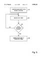
- FIG. 6shows a method of operating the spindle motor 14.
- the methodincludes the steps of generating a control signal representing an average voltage for the spindle motor (step 200), generating a PWM signal having a duty cycle that is inversely proportional to magnitude of the power supply potential and is directly proportional to the control signal representing average spindle motor voltage (step 202); and using the PWM signal to operate the power driver stage in a switched voltage mode (step 204).
- a zero-crossingis found (step 206).
- Back emfwhich is used for speed feedback, is thereafter detected at a constant period (step 208).
- the microprocessor chip 24supplies the uncompensated motor voltage signal UMVS to the duty cycle-to-dc converter 50, which includes transistors Q1, Q2, Q3 and Q4.
- Transistor Q2receives current from the voltage control signal, and the current is mirrored in transistors Q3 and Q4.
- the transistors Q1 to Q4avoid power supply variations.
- Mirrored current Ipdccharges a capacitor Cdc which, with resistor Rdc, forms a simple RC network.
- Voltage on the capacitor Cdcis amplified by amplifier SR, the gain of which is determined by resistors R8 and R9.
- An output of the gain amplifier SRprovides the control signal CS representing the average spindle motor voltage.
- a digital to analog convertercould be used in place of the transistors Q1 to Q4.
- Transistors Q6 and Q7form the current source 56, and resistors R10 and R11 form the resistive ladder 54.
- the currentflows around the transistors Q6 and Q7 and into the capacitor 58.
- the capacitor 58is charged with the current from the current source 52.
- the second comparator 66compares the voltage on the capacitor 58 to a percentage of the power bus voltage Vpwr. When the output of the second comparator 66 goes high, the one shot 62 generates a pulse.
- the one-shot 62is formed by gates U4B, U3B and U4C. The pulse causes the capacitor 58 to discharge through the transistor 64.
- the ramped sawtooth waveformis supplied to the inverting input of the first comparator 52, and an output of the gain amplifier SR is supplied to the non-inverting input of the first comparator 52.
- the output of the first comparator 52provides the PWM signal.
- FIGS. 8 and 9show other embodiments of the invention.
- FIG. 8shows that the disk controller chip 126 can generate the uncompensated motor voltage signal UMVS instead of the microprocessor chip.
- FIG. 9shows that pulse width modulation can be performed in power driver stage 136 instead of the commutation logic 138.
- the timing signal SP -- CLKis supplied to the commutation logic 138, and unmodulated commutation commands COM are provided to the power driver stage 136.
- the PWM signalis provided directly to the power driver stage 136.
- the power driver stage 136includes an extra solid state driver for performing pulse width modulation.
Landscapes
- Engineering & Computer Science (AREA)
- Power Engineering (AREA)
- Control Of Motors That Do Not Use Commutators (AREA)
Abstract
Description
______________________________________State A B C______________________________________1 1 X 02X 1 03 0 1 X4 0X 15 X 0 16 1 0 X______________________________________
Ton/T=Vdc/KVpwr
Claims (10)
Priority Applications (1)
| Application Number | Priority Date | Filing Date | Title |
|---|---|---|---|
| US08/972,939US5898283A (en) | 1997-11-18 | 1997-11-18 | Voltage feedforward control system for a spindle motor of a disk drive |
Applications Claiming Priority (1)
| Application Number | Priority Date | Filing Date | Title |
|---|---|---|---|
| US08/972,939US5898283A (en) | 1997-11-18 | 1997-11-18 | Voltage feedforward control system for a spindle motor of a disk drive |
Publications (1)
| Publication Number | Publication Date |
|---|---|
| US5898283Atrue US5898283A (en) | 1999-04-27 |
Family
ID=25520316
Family Applications (1)
| Application Number | Title | Priority Date | Filing Date |
|---|---|---|---|
| US08/972,939Expired - LifetimeUS5898283A (en) | 1997-11-18 | 1997-11-18 | Voltage feedforward control system for a spindle motor of a disk drive |
Country Status (1)
| Country | Link |
|---|---|
| US (1) | US5898283A (en) |
Cited By (22)
| Publication number | Priority date | Publication date | Assignee | Title |
|---|---|---|---|---|
| US6462496B1 (en) | 1999-11-23 | 2002-10-08 | Texas Instruments Incorporated | Current mode approach to spindle motor current control and rotor position sense |
| US6617817B2 (en)* | 2001-06-01 | 2003-09-09 | Stmicroelectronics, Ltd. | Electrical time constant compensation method for switched, voltage-mode driver circuit |
| US20030198157A1 (en)* | 2002-04-19 | 2003-10-23 | Gateway, Inc. | Method of CD/DVD vibration detection by monitoring motor conditions |
| EP1372259A1 (en)* | 2002-06-14 | 2003-12-17 | STMicroelectronics S.r.l. | Method and apparatus for driving complex impedance loads in voltage-mode |
| US20040036999A1 (en)* | 2002-06-14 | 2004-02-26 | Stmicroelectronics S.R.I. | Voltage-mode drive for driving complex impedance loads |
| US6850384B1 (en) | 2003-02-28 | 2005-02-01 | Western Digital Technologies, Inc. | Disk drive comprising oscillators and counters for sensing current in a voice coil motor |
| US6934135B1 (en) | 2003-02-28 | 2005-08-23 | Western Digital Technologies, Inc. | Disk drive monitoring a supply current to protect motor driver circuits |
| US6967458B1 (en) | 2002-07-31 | 2005-11-22 | Western Digital Technologies, Inc. | Decreasing spin up time in a disk drive by adjusting a duty cycle of a spindle motor PWM signal to maintain constant average input current |
| US6970319B1 (en) | 2003-05-27 | 2005-11-29 | Western Digital Technologies, Inc. | Disk drive comprising a pulse width modulated demand limit circuit for enhancing power management during spin-down |
| US7012396B1 (en) | 2004-09-30 | 2006-03-14 | Agere Systems Inc. | Increased digital spindle motor control resolution through dither |
| US20060066280A1 (en)* | 2004-09-30 | 2006-03-30 | Jaydip Bhaumik | Digital spindle control architecture |
| US20070053096A1 (en)* | 2005-09-02 | 2007-03-08 | Samsung Electronics Co., Ltd. | Hard disk drive, method for parking magnetic head of hard disk drive, and computer readable recording medium recording the method |
| US7209321B1 (en) | 2003-07-31 | 2007-04-24 | Western Digital Technologies, Inc. | Disk drive pulse width modulating a voice coil motor using model reference current feedback |
| US20100145538A1 (en)* | 2005-03-30 | 2010-06-10 | Koninklijke Philips Electronics, N.V. | Method of limiting a power supply current and optical device |
| US8610391B1 (en) | 2011-06-29 | 2013-12-17 | Western Digital Technologies, Inc. | Disk drive optimizing spindle motor torque by adjusting leading phase angle during spin-up |
| US8649121B1 (en) | 2012-03-28 | 2014-02-11 | Western Digital Technologies, Inc. | Disk drive tuning speed control loop for a spindle motor |
| US8737008B1 (en) | 2011-05-12 | 2014-05-27 | Western Digital Technologies, Inc. | Disk drive adjusting gain of spindle motor compensator based on a ratio of spin speeds |
| US8830617B1 (en) | 2013-05-30 | 2014-09-09 | Western Digital Technologies, Inc. | Disk drive adjusting state estimator to compensate for unreliable servo data |
| US8982501B1 (en) | 2014-09-22 | 2015-03-17 | Western Digital Technologies, Inc. | Data storage device compensating for repeatable disturbance when commutating a spindle motor |
| US9099147B1 (en) | 2014-09-22 | 2015-08-04 | Western Digital Technologies, Inc. | Data storage device commutating a spindle motor using closed-loop rotation phase alignment |
| US9171568B1 (en) | 2014-06-25 | 2015-10-27 | Western Digital Technologies, Inc. | Data storage device periodically re-initializing spindle motor commutation sequence based on timing data |
| US9230592B1 (en) | 2014-12-23 | 2016-01-05 | Western Digital Technologies, Inc. | Electronic system with a method of motor spindle bandwidth estimation and calibration thereof |
Citations (12)
| Publication number | Priority date | Publication date | Assignee | Title |
|---|---|---|---|---|
| US4541039A (en)* | 1984-01-25 | 1985-09-10 | Venus Scientific Inc. | Magnetically modulated d-c to d-c forward converter power supply |
| US4764856A (en)* | 1987-01-23 | 1988-08-16 | U.S. Philips Corporation | Power-supply arrangement |
| US4791544A (en)* | 1984-09-21 | 1988-12-13 | Veeco Instruments | Regulating control for single-ended switching power supply |
| US4809150A (en)* | 1988-01-27 | 1989-02-28 | Electric Power Research Institute, Inc. | DC to DC converter with feed forward and feed back regulation |
| US4862054A (en)* | 1988-10-31 | 1989-08-29 | Westinghouse Electric Corp. | Tacho-less vector control adaptive system for motor drive |
| US4933829A (en)* | 1988-03-24 | 1990-06-12 | Compaq Computer Corporation | Free running flyback DC power supply with current limit circuit |
| US4996638A (en)* | 1990-02-15 | 1991-02-26 | Northern Telecom Limited | Method of feedback regulating a flyback power converter |
| US5117347A (en)* | 1990-05-10 | 1992-05-26 | Teledyne Industries, Inc. | Full duty cycle forward converter |
| US5204593A (en)* | 1991-11-08 | 1993-04-20 | Victor Company Of Japan, Ltd. | Drive system for information recording/reproducing apparatus |
| US5241251A (en)* | 1990-05-21 | 1993-08-31 | Asahi Kogaku Kogyo Kabushiki Kaisha | Drive signal generating device |
| US5757751A (en)* | 1996-01-16 | 1998-05-26 | International Business Machines Corporation | Baseline correction circuit for pulse width modulated data readback systems |
| US5760563A (en)* | 1996-06-28 | 1998-06-02 | Western Digital Corporation | Method and apparatus for providing thermal feedback between an analog power chip and a digital controller chip in a disk controller system |
- 1997
- 1997-11-18USUS08/972,939patent/US5898283A/ennot_activeExpired - Lifetime
Patent Citations (12)
| Publication number | Priority date | Publication date | Assignee | Title |
|---|---|---|---|---|
| US4541039A (en)* | 1984-01-25 | 1985-09-10 | Venus Scientific Inc. | Magnetically modulated d-c to d-c forward converter power supply |
| US4791544A (en)* | 1984-09-21 | 1988-12-13 | Veeco Instruments | Regulating control for single-ended switching power supply |
| US4764856A (en)* | 1987-01-23 | 1988-08-16 | U.S. Philips Corporation | Power-supply arrangement |
| US4809150A (en)* | 1988-01-27 | 1989-02-28 | Electric Power Research Institute, Inc. | DC to DC converter with feed forward and feed back regulation |
| US4933829A (en)* | 1988-03-24 | 1990-06-12 | Compaq Computer Corporation | Free running flyback DC power supply with current limit circuit |
| US4862054A (en)* | 1988-10-31 | 1989-08-29 | Westinghouse Electric Corp. | Tacho-less vector control adaptive system for motor drive |
| US4996638A (en)* | 1990-02-15 | 1991-02-26 | Northern Telecom Limited | Method of feedback regulating a flyback power converter |
| US5117347A (en)* | 1990-05-10 | 1992-05-26 | Teledyne Industries, Inc. | Full duty cycle forward converter |
| US5241251A (en)* | 1990-05-21 | 1993-08-31 | Asahi Kogaku Kogyo Kabushiki Kaisha | Drive signal generating device |
| US5204593A (en)* | 1991-11-08 | 1993-04-20 | Victor Company Of Japan, Ltd. | Drive system for information recording/reproducing apparatus |
| US5757751A (en)* | 1996-01-16 | 1998-05-26 | International Business Machines Corporation | Baseline correction circuit for pulse width modulated data readback systems |
| US5760563A (en)* | 1996-06-28 | 1998-06-02 | Western Digital Corporation | Method and apparatus for providing thermal feedback between an analog power chip and a digital controller chip in a disk controller system |
Cited By (27)
| Publication number | Priority date | Publication date | Assignee | Title |
|---|---|---|---|---|
| US6462496B1 (en) | 1999-11-23 | 2002-10-08 | Texas Instruments Incorporated | Current mode approach to spindle motor current control and rotor position sense |
| US6617817B2 (en)* | 2001-06-01 | 2003-09-09 | Stmicroelectronics, Ltd. | Electrical time constant compensation method for switched, voltage-mode driver circuit |
| US20030198157A1 (en)* | 2002-04-19 | 2003-10-23 | Gateway, Inc. | Method of CD/DVD vibration detection by monitoring motor conditions |
| US7130255B2 (en)* | 2002-04-19 | 2006-10-31 | Gateway Inc. | Method of CD/DVD vibration detection by monitoring motor conditions |
| EP1372259A1 (en)* | 2002-06-14 | 2003-12-17 | STMicroelectronics S.r.l. | Method and apparatus for driving complex impedance loads in voltage-mode |
| US20040036999A1 (en)* | 2002-06-14 | 2004-02-26 | Stmicroelectronics S.R.I. | Voltage-mode drive for driving complex impedance loads |
| US6940685B2 (en) | 2002-06-14 | 2005-09-06 | Stmicroelectronics S.R.L. | Voltage-mode drive for driving complex impedance loads |
| US6967458B1 (en) | 2002-07-31 | 2005-11-22 | Western Digital Technologies, Inc. | Decreasing spin up time in a disk drive by adjusting a duty cycle of a spindle motor PWM signal to maintain constant average input current |
| US6850384B1 (en) | 2003-02-28 | 2005-02-01 | Western Digital Technologies, Inc. | Disk drive comprising oscillators and counters for sensing current in a voice coil motor |
| US6934135B1 (en) | 2003-02-28 | 2005-08-23 | Western Digital Technologies, Inc. | Disk drive monitoring a supply current to protect motor driver circuits |
| US6970319B1 (en) | 2003-05-27 | 2005-11-29 | Western Digital Technologies, Inc. | Disk drive comprising a pulse width modulated demand limit circuit for enhancing power management during spin-down |
| US7209321B1 (en) | 2003-07-31 | 2007-04-24 | Western Digital Technologies, Inc. | Disk drive pulse width modulating a voice coil motor using model reference current feedback |
| US20060066280A1 (en)* | 2004-09-30 | 2006-03-30 | Jaydip Bhaumik | Digital spindle control architecture |
| US20060066279A1 (en)* | 2004-09-30 | 2006-03-30 | Agere Systems Inc. | Increased digital spindle motor control resolution through dither |
| US7012396B1 (en) | 2004-09-30 | 2006-03-14 | Agere Systems Inc. | Increased digital spindle motor control resolution through dither |
| US7034478B2 (en)* | 2004-09-30 | 2006-04-25 | Agere Systems Inc. | Digital spindle control architecture |
| US20100145538A1 (en)* | 2005-03-30 | 2010-06-10 | Koninklijke Philips Electronics, N.V. | Method of limiting a power supply current and optical device |
| US20070053096A1 (en)* | 2005-09-02 | 2007-03-08 | Samsung Electronics Co., Ltd. | Hard disk drive, method for parking magnetic head of hard disk drive, and computer readable recording medium recording the method |
| US7952828B2 (en)* | 2005-09-02 | 2011-05-31 | Samsung Electronics Co., Ltd. | Hard disk drive, method for parking magnetic head of hard disk drive, and computer readable recording medium recording the method |
| US8737008B1 (en) | 2011-05-12 | 2014-05-27 | Western Digital Technologies, Inc. | Disk drive adjusting gain of spindle motor compensator based on a ratio of spin speeds |
| US8610391B1 (en) | 2011-06-29 | 2013-12-17 | Western Digital Technologies, Inc. | Disk drive optimizing spindle motor torque by adjusting leading phase angle during spin-up |
| US8649121B1 (en) | 2012-03-28 | 2014-02-11 | Western Digital Technologies, Inc. | Disk drive tuning speed control loop for a spindle motor |
| US8830617B1 (en) | 2013-05-30 | 2014-09-09 | Western Digital Technologies, Inc. | Disk drive adjusting state estimator to compensate for unreliable servo data |
| US9171568B1 (en) | 2014-06-25 | 2015-10-27 | Western Digital Technologies, Inc. | Data storage device periodically re-initializing spindle motor commutation sequence based on timing data |
| US8982501B1 (en) | 2014-09-22 | 2015-03-17 | Western Digital Technologies, Inc. | Data storage device compensating for repeatable disturbance when commutating a spindle motor |
| US9099147B1 (en) | 2014-09-22 | 2015-08-04 | Western Digital Technologies, Inc. | Data storage device commutating a spindle motor using closed-loop rotation phase alignment |
| US9230592B1 (en) | 2014-12-23 | 2016-01-05 | Western Digital Technologies, Inc. | Electronic system with a method of motor spindle bandwidth estimation and calibration thereof |
Similar Documents
| Publication | Publication Date | Title |
|---|---|---|
| US5898283A (en) | Voltage feedforward control system for a spindle motor of a disk drive | |
| US5986426A (en) | Adaptive pulse width modulated motor control | |
| US6252362B1 (en) | Method and apparatus for synchronizing PWM sinusoidal drive to a DC motor | |
| KR100755532B1 (en) | Method and apparatus for driving multiphase, brushless DC motor | |
| US5204593A (en) | Drive system for information recording/reproducing apparatus | |
| US5289097A (en) | Spindle control method and apparatus for disk drive | |
| US5569988A (en) | Brushless motor drive circuit including a linear amplifier for sending and output signal based upon the detected back electromotive force voltage | |
| US6998801B2 (en) | Motor drive device and motor drive integrated circuit device | |
| US6967458B1 (en) | Decreasing spin up time in a disk drive by adjusting a duty cycle of a spindle motor PWM signal to maintain constant average input current | |
| US6498446B1 (en) | System and method for optimizing torque in a polyphase disk drive motor | |
| US6753667B2 (en) | Method and apparatus for controlling spindle motor to match plural modes of operation in a disk drive | |
| JP2009505618A (en) | Brushless motor driving device and data reading / writing device having brushless motor controlled by such driving device | |
| KR100280581B1 (en) | Direct Access Memory (DASD) with Variable Spindle Rotation Speed | |
| US20020001153A1 (en) | Fully digital control and drive combination IC with on-board DSP for disk mass storage device | |
| JPH10341588A (en) | Current zerocross detection of inductive load, and optimization of voltage mode pwm drive | |
| JP3114733B2 (en) | Spindle motor drive circuit | |
| US20020027423A1 (en) | Method and circuit for driving a brushless dc motor to reduce low acoustic noise | |
| US6707269B2 (en) | Motor control circuit with adaptive dynamic range selection | |
| US6065231A (en) | Motor drive method and drive circuit | |
| KR20010094966A (en) | System, method, and program product for controlling commutation of disk drive motor | |
| EP1003275B1 (en) | Method and system for driving a three-phase motor in a mass storage device | |
| JP2526442B2 (en) | Disk unit | |
| JPH11191251A (en) | Recording and playback device | |
| JPH06195858A (en) | Data recording / reproducing apparatus and motor drive control method used in the apparatus |
Legal Events
| Date | Code | Title | Description |
|---|---|---|---|
| AS | Assignment | Owner name:WESTERN DIGITAL CORPORATION, CALIFORNIA Free format text:ASSIGNMENT OF ASSIGNORS INTEREST;ASSIGNOR:BENNETT, GEORGE JEFFREY;REEL/FRAME:009032/0506 Effective date:19971210 | |
| AS | Assignment | Owner name:BANKBOSTON, N.A., AS AGENT, MASSACHUSETTS Free format text:PATENT COLLATERAL ASSIGNMENT AND SECURITY AGREEMENT DATED AS OF NOVEMBER 4, 1998;ASSIGNOR:WESTERN DIGITAL CORPORATION, A DELAWARE CORPORATION;REEL/FRAME:009596/0487 Effective date:19981104 | |
| STCF | Information on status: patent grant | Free format text:PATENTED CASE | |
| AS | Assignment | Owner name:WESTERN DIGITAL CORPORATION, CALIFORNIA Free format text:RELEASE BY SECURED PARTY;ASSIGNOR:FLEET NATIONAL BANK (F/K/A BANKBOSTON, N.A.);REEL/FRAME:011089/0459 Effective date:20000330 | |
| AS | Assignment | Owner name:GENERAL ELECTRIC CAPITAL CORPORATION, CALIFORNIA Free format text:SECURITY AGREEMENT;ASSIGNOR:WESTERN DIGITAL CORPORATION;REEL/FRAME:011170/0948 Effective date:20000920 | |
| AS | Assignment | Owner name:WESTERN DIGITAL TECHNOLOGIES, INC., CALIFORNIA Free format text:AMENDED AND RESTATED CERTIFICATE OF INCORPORATION OF WESTERN DIGITAL CORP.;ASSIGNOR:WESTERN DIGITAL CORPORATION;REEL/FRAME:011967/0481 Effective date:20010406 | |
| FPAY | Fee payment | Year of fee payment:4 | |
| FPAY | Fee payment | Year of fee payment:8 | |
| AS | Assignment | Owner name:WESTERN DIGITAL TECHNOLOGIES, INC., CALIFORNIA Free format text:RELEASE BY SECURED PARTY;ASSIGNOR:GENERAL ELECTRIC CAPITAL CORPORATION, AS AGENT;REEL/FRAME:021502/0451 Effective date:20070809 | |
| REMI | Maintenance fee reminder mailed | ||
| FPAY | Fee payment | Year of fee payment:12 | |
| SULP | Surcharge for late payment | Year of fee payment:11 |