US5897354A - Method of forming a non-volatile memory device with ramped tunnel dielectric layer - Google Patents
Method of forming a non-volatile memory device with ramped tunnel dielectric layerDownload PDFInfo
- Publication number
- US5897354A US5897354AUS08/768,885US76888596AUS5897354AUS 5897354 AUS5897354 AUS 5897354AUS 76888596 AUS76888596 AUS 76888596AUS 5897354 AUS5897354 AUS 5897354A
- Authority
- US
- United States
- Prior art keywords
- dielectric layer
- gate material
- thickness
- region edge
- floating gate
- Prior art date
- Legal status (The legal status is an assumption and is not a legal conclusion. Google has not performed a legal analysis and makes no representation as to the accuracy of the status listed.)
- Expired - Lifetime
Links
Images

Classifications
- H—ELECTRICITY
- H10—SEMICONDUCTOR DEVICES; ELECTRIC SOLID-STATE DEVICES NOT OTHERWISE PROVIDED FOR
- H10D—INORGANIC ELECTRIC SEMICONDUCTOR DEVICES
- H10D30/00—Field-effect transistors [FET]
- H10D30/01—Manufacture or treatment
- H10D30/021—Manufacture or treatment of FETs having insulated gates [IGFET]
- H10D30/0411—Manufacture or treatment of FETs having insulated gates [IGFET] of FETs having floating gates
- H—ELECTRICITY
- H10—SEMICONDUCTOR DEVICES; ELECTRIC SOLID-STATE DEVICES NOT OTHERWISE PROVIDED FOR
- H10D—INORGANIC ELECTRIC SEMICONDUCTOR DEVICES
- H10D30/00—Field-effect transistors [FET]
- H10D30/60—Insulated-gate field-effect transistors [IGFET]
- H10D30/68—Floating-gate IGFETs
- H10D30/6891—Floating-gate IGFETs characterised by the shapes, relative sizes or dispositions of the floating gate electrode
- Y—GENERAL TAGGING OF NEW TECHNOLOGICAL DEVELOPMENTS; GENERAL TAGGING OF CROSS-SECTIONAL TECHNOLOGIES SPANNING OVER SEVERAL SECTIONS OF THE IPC; TECHNICAL SUBJECTS COVERED BY FORMER USPC CROSS-REFERENCE ART COLLECTIONS [XRACs] AND DIGESTS
- Y10—TECHNICAL SUBJECTS COVERED BY FORMER USPC
- Y10S—TECHNICAL SUBJECTS COVERED BY FORMER USPC CROSS-REFERENCE ART COLLECTIONS [XRACs] AND DIGESTS
- Y10S438/00—Semiconductor device manufacturing: process
- Y10S438/981—Utilizing varying dielectric thickness
Definitions
- the inventionrelates to a non-volatile memory or EPROM device with a ramped tunnel dielectric layer, a memory array containing such a non-volatile memory device, a method of making such a non-volatile memory, a method of programming such non-volatile memory or and a method of reading such a programmed non-volatile memory device.
- MOSMetal-oxide-semiconductor
- EPROMselectronically programmable read-only memories
- EEPROMserasable electronically programmable read-only memories
- flash memorycan be programmed by hot electron techniques. The entire contents of the flash memory can be erased electronically in a single operation (e.g., universal change by Fowler-Nordheim tunneling).
- FIG. 1The general structure of an EPROM memory cell or transistor 10, is shown in FIG. 1.
- This transistorhas a semiconducting substrate 15, a source region 13, a drain region 14, a tunnel dielectric layer on the substrate 16, a floating gate 12, an interpoly dielectric layer 17 on the floating gate and a control gate 11 on said interpoly dielectric layer.
- the floating gate 12is electrically isolated from the semiconductor substrate by the tunnel dielectric layer and from the control gate by the interpoly dielectric, and stores information in the form of charge.
- a flash EPROMis made from a plurality of these transistors, interconnected so that they can be individually programmed, and erased in blocks or groups.
- EEPROMsare electronically programmable and erasable.
- One way to program an individual EPROM cellis to apply a voltage between the source and the control gate, as well as a voltage between the source and the drain.
- the source-drain voltagegenerates hot electrons that are swept across the channel from the source to the drain.
- the voltage on the control gateallows hot electrons in the channel to be injected onto the floating gate thereby raising the threshold voltage.
- the state of the floating gate, on or off,can be determined by applying a voltage between the source and the drain.
- An EEPROM memory cellcan be erased by removing electrons from the floating gate. This can be accomplished using Fowler-Nordheim tunneling. In this process a voltage is applied between the control gate and the source. This creates an electric field across the tunnel dielectric layer between the floating gate and the source, causing electrons to be removed from the floating gate.
- a problem suffered by traditional EEPROMsis the degradation of the tunnel dielectric layer due to introduction of hot electrons. Over time, the cumulative effects of hot electron damage can result in catastrophic failure of the memory device observed as data retention failure. Due to the susceptibility of these devices to catastrophic failure, the reliability of such devices could be improved. While the reliability of some non-volatile memory devices has been increased, such increases in reliability have been at the expense of access speed in writing and programing.
- one object of the inventionis to provide a non-volatile memory (NVM) with a ramped tunnel dielectric layer.
- NVMnon-volatile memory
- Another object of the inventionis to provide an array of non-volatile memory devices with ramped tunnel dielectric layers.
- Another object of the inventionis to provide a method of making a non-volatile memory device with a ramped tunnel dielectric layer.
- Another object of the inventionis to provide a method of reading a programmed non-volatile memory device.
- Another object of the inventionis to provide a method of programming a non-volatile memory device.
- non-volatile memory devicecomprising sequentially:
- tunnel dielectric layerhas a thickness at the drain region edge greater than at the source region edge.
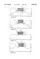
- FIG. 1shows a general structure for a transistor containing a floating gate
- FIG. 2shows a floating gate transistor having a tunnel dielectric layer thickness which is greater at the drain region edge than at the source region edge;
- FIG. 3shows a floating gate transistor having a ramped or tapered tunnel dielectric thickness
- FIG. 4illustrates a stage in the manufacture of a non-volatile memory in which an oxidation mask is formed over a portion of the control gate, prior to oxidation;
- FIG. 5illustrates a stage in the manufacture of a non-volatile memory in which oxidation of the control and floating gate material layers in the presence of an oxidation mask has been performed.
- FIG. 2depicts a basic non-volatile memory or flash memory device having a ramped tunnel dielectric layer thickness.
- the control gate and floating gate systemsare disposed over a channel between source region 2 and drain region 3.
- the tunnel dielectric layer 10has a drain region edge 12 and a source region edge.
- Optional channel stops 13 and 14are illustrated. Additional elements such as contact electrodes and passivation layers have been omitted for clarity.
- Layers 6, 7, 9 and 10may be layered sequentially on the substrate.
- the substrate 1may be a semiconductor material conventionally known by those of ordinary skill in the art. Examples include silicon, gallium arsenide, germanium, gallium nitride, aluminum phosphide, and alloys such as Si 1-x Ge x and Al x Ga 1-x As, where 0 ⁇ 1. Many others are known, such as those listed in Semiconductor Device Fundamentals, on page 4, Table 1.1 (Robert F. Pierret, Addison-Wesley, 1996). Preferably, the substrate is silicon. Such substrates may be formed epitaxially in accordance with conventional techniques. Doping techniques known to those of ordinary skill in the art may be used to adjust the conductivity properties of the semiconductor substrate. Furthermore, the substrate often may have a top layer of an oxide, such as silicon oxide, to protect the substrate and/or the tunnel dielectric layer of a transistor.
- an oxidesuch as silicon oxide
- the source and drain regions (2 and 3)may be formed in the substrate by methods well known to those of ordinary skill in the art.
- the substrate or wellis p-type and the source and drain regions are n-type.
- the floating gate material 9 of the floating gate system 8may comprise a highly doped polysilicon or amorphous silicon (polysilicon), an alloy of a conductive metal with silicon (a so-called "silicide” such as, for example, titanium silicide, tungsten silicide, aluminum silicide or copper silicide), or a combination thereof.
- a so-called "silicide”such as, for example, titanium silicide, tungsten silicide, aluminum silicide or copper silicide
- Such combinationsmay comprise a plurality of layers wherein each layer may comprise or consist of an independently selected floating gate material.
- the resistivity of siliconcan be controlled over a wide range by varying the concentration of impurities such as phosphorous, boron and arsenic, as described in Microchip Fabrication, Peter Van Zant, pp 21-42 (McGraw-Hill, 1990).
- the floating gate material layermay comprise a silicide such as cobalt silicide, hafnium silicide, molybdenum silicide, nickel silicide, palladium silicide, platinum silicide, tantalum silicide, titanium silicide, tungsten silicide, zirconium silicide and chromium silicide.
- the floating gate material layercomprises polysilicon, either doped or undoped.
- the floating gate material layermay be doped with one or more dopants selected from the group consisting of B, P, As and Sb in an amount of 1 ⁇ 10 18 -5 ⁇ 10 21 atoms/cm 3 , more preferably 1 ⁇ 10 19 -5 ⁇ 10 20 atoms/cm 3 .
- the floating gate material layermay have a resistivity of from 25 to 2,000 ⁇ / ⁇ , more preferably a resistivity of from 150-250 ⁇ / ⁇ and even more preferably about 200 ⁇ / ⁇ .
- the resistivitymay be proportional to the thickness of the layer.
- a 2,000 ⁇ thick floating gate material layermay have a resistivity of from 150-250 ⁇ / ⁇ , preferably about 200 ⁇ / ⁇ .
- a 1,000 ⁇ thick floating gate material layermay have a resistivity of from 350-450 ⁇ / ⁇ , preferably about 400 ⁇ / ⁇ .
- the device according to the present inventionis similar to a conventional non-volatile memory device except that the thickness of the dielectric layer is greater at the drain region edge than at the source region edge.
- the ratio of the tunnel dielectric layer thickness at the drain region edge to the tunnel dielectric layer thickness at the source region edgeis >1:1, preferably ⁇ 1.1:1, more preferably ⁇ 1.2:1, most preferably about 1.5:1. In further embodiments, this ratio ranges up to about 100:1, preferably up to about 40:1, more preferably up to about 10:1 and most preferably up to about 4:1.
- the thickness of the tunnel dielectric layerincreases continually from its source region edge to its drain region edge (i.e., in the direction from the source, across the channel, to the drain), such that at any point along the length of the channel, the tunnel dielectric layer thickness on the side of the drain region (TDt d ) is greater than or equal to the tunnel dielectric layer thickness on the side of the source region (TDt s ), but at one or more such points, TDt d >TDt s . More preferably, the tunnel dielectric layer thickness, beginning at the source region edge and moving to the drain region edge, across the length of the channel, will increase steadily in a ramped fashion.
- FIGS. 2-5have been provided to illustrate certain aspects of the invention.
- the specific details of the composition of the floating gate material layer, tunnel dielectric layer, control gate material layer, interpoly dielectric, semiconductor, source and drain regionsare not limited by the Figures.
- the illustrations in FIGS. 4 and 5depict the presence of sidewall oxide spacers, the presence of which is optional to the practice of the claimed invention.
- the absolute dimensions of the tunnel dielectric layer thickness at the source sideis not particularly limited, and may vary depending on the desired characteristics of the device. Generally, the thickness of the tunnel dielectric layer at the source region edge ranges from 30 to 3000 ⁇ , preferably from 50 to 200 ⁇ , more preferably about 70 to about 100 ⁇ .
- the thickness of the tunnel dielectric layer at the drain region edge 12is not particularly limited, provided that the thickness at the drain region edge 12 is greater than the thickness at the source region edge.
- the thickness at the drain region edge 12is from 10 to 1,000 ⁇ greater than the thickness at the source region edge, more preferably 20 to 200 ⁇ , and even more preferably 50 to 100 ⁇ .
- the tunnel dielectric layer material 10may be one conventionally known to those of ordinary skill in the art. Non-limiting examples include silicon dioxide, silicon oxynitride (SiO x N y ), metal nitrides (such as Si 3 N 4 ), V 2 O 5 , tetraethylorthosilicate-based silicon oxides and titanium oxide. Accordingly, the may not necessarily be an oxide, but may simply be any material functioning as an electrical insulation layer between the floating gate material layer and the substrate. The may be modified by the addition of boron, phosphorous or both. SiO 2 and SiO 2 -based films can be formed from thermal oxides; silane, tetraethoxysilane, borophosphosilicate glass and spin-on-glass.
- the tunnel dielectriccomprises an oxide of the corresponding floating gate material layer 9. More preferably, the tunnel dielectric layer 10 comprises a silicon dioxide layer and the floating gate material layer 9 comprises polysilicon, which is preferably doped, as described above.
- the channel lengthis the distance between the source and drain regions 2 and 3 and will typically be from 0.1 to 100 ⁇ m, preferably from 0.18 to 10 ⁇ m, more preferably from 0.25 to 2 ⁇ m.
- the floating gate material layerwill preferably have a thickness (height) of from 500 to 8,000 ⁇ , more preferably from 1,000 to 5,000 ⁇ , even more preferably from 1,500 to about 3,000 ⁇ .
- the floating gate material layermay have a different thickness at its drain region edge relative to its source region.
- the floating gate material layer thickness (FGt)may be complementary to the tunnel dielectric layer thickness (TDt) as illustrated in FIG. 2 such that after planarization, at any number of points along the length of the channel, the average sum of FGt+TDt is a Constant (e.g., to two significant figures).
- the thickness of the floating gate material layermay be uniform across the interface with the tunnel dielectric layer, such that the profile of the floating gate system 8 is thicker at the drain region side than at the source region side.
- the channelwill also have a width dimension, perpendicular to the plane of the page (the "X-Y" axes) as depicted in FIGS. 2 and 3.
- the width of the channelmay vary depending on the desired electronic characteristics. Typically the channel width ranges from 0.1 to 2,000 ⁇ m, preferably from 0.1 to 1,000 ⁇ m, more preferably from 0.4 to 100 ⁇ M.
- the doping of the semiconductor substrate to form source and drain regions 2 and 3may be conducted by methods known to those of ordinary skill in the art, using materials known to those of ordinary skill in the art for their known purposes.
- n-type and p-type doping of a semiconductor substratemay be accomplished by conventional methods known to those of ordinary skill in the art.
- Dopant speciessuch as arsenic, antimony, phosphorus, and boron may be added by well known techniques such as ion implantation or diffusion.
- a p-type substrateis doped to form n-type source and drain regions.
- Implantationmay be followed by annealing and/or "drive-in" steps to deliver the dopant in a desired fashion. Such annealing and drive-in steps may be conducted by conventional methods known to those of ordinary skill in the art.
- the locations of the source and drain regionsmay be self-aligned with the floating gate material layer.
- the devicemay also be equipped with a lightly doped n-type extension at the source region.
- a lightly doped n-type extensionis conventional and known to those of skill in the art (see for example U.S. Pat. No. 4,356,623, incorporated herewith by reference).
- An n-type extension on the drain regionshould not be used, as such would inhibit the programming of the floating gate system.
- a sidewall oxidemay be added to the wall of the patterned floating gate material layer.
- the sidewall oxide and floating gate material layeract to align the highly doped region of the source to the floating gate system.
- the device of the present inventionis equipped with a control gate electrode, disposed over said floating gate material layer, which comprises a control gate material layer and an interpoly dielectric layer.
- the interpoly dielectric material 7may be one conventionally known to those of ordinary skill in the art. Non-limiting examples include silicon dioxide, oxide/nitride/oxide (ONO), silicon oxynitride (SiO x N y ) metal nitrides such as Si 3 N 4 , V 2 O 5 , tetraethylorthosilicate-based oxides and titanium oxide. Accordingly, the interpoly dielectric material need not necessarily be an oxide, but simply function as an insulation layer between the control gate material layer and the floating gate material layer. The interpoly dielectric material 7 may be modified by the addition of boron, phosphorous or both.
- SiO 2 and SiO 2 -based filmscan be formed from thermal oxides, silane, tetraethoxysilane, borophosphosilicate glass and spin-on-glass.
- the interpoly dielectric material 7comprises an oxide of the corresponding control gate material layer 6.
- the interpoly dielectric layer 7comprises an oxide/nitride/oxide (ONO) layer.
- the thickness of the interpoly dielectric layeris preferably from 100 to 500 ⁇ , more preferably from 200 to 300 ⁇ .
- control gate material layer 6may comprise any gate material layer conventionally known to those of ordinary skill in the art
- control gate material layerinclude polysilicon and silicides such as cobalt silicide, hafnium silicide, molybdenum silicide, nickel silicide, palladium silicide, platinum silicide, tantalum silicide, titanium silicide, tungsten silicide, zirconium silicide and chromium silicide.
- the interpoly dielectric 7comprises an oxide/nitride/oxide (ONO) layer and the control gate material layer 6 is polysilicon, which may be doped or undoped as described above.
- ONOoxide/nitride/oxide
- the thickness of the control gate material layeris preferably from 1,000 to 5,000 ⁇ , more preferably 2,000 to 4,000 ⁇ , even more preferably about 3,000 ⁇ .
- the thickness of the interpoly dielectric layermay be uniform across the interface with the floating gate material layer.
- the control gatehas an interpoly dielectric layer having a drain region edge and a source region edge and a ramped thickness which is thicker at the drain region edge then at the source region edge.
- the ratio of the interpoly dielectric layer thickness at the drain region edge to the interpoly dielectric layer thickness at the source region edgeis >1:1, preferably ⁇ 1.1:1, more preferably ⁇ 1.2:1, most preferably about 2.5:1.
- the upper limitis ratio ranges up to about 100:1, preferably up to about 40:1, more preferably up to about 10:1 and most preferably up to about 4:1.
- the thickness of the interpoly dielectric layercontinually increases from its source region edge to its drain region edge (i.e., in the direction from the source, across the channel, to the drain), such that at any statistically significant number of points along the length of the channel, the average interpoly dielectric layer thickness on the side of the drain region (IDt d ) is>the average interpoly dielectric layer thickness on the side of the source region (IDt s ), but at one or more such points, IDt d >IDt s .
- the interpoly dielectric layer thickness, beginning at the source region edge and moving to the drain region edge, across the length of the channelwill increase steadily in a ramped fashion. In other words, there is a gradual increase in the thickness of the interpoly dielectric layer in the direction from the source region edge to the drain region edge.
- the control gate material layermay have a different thickness at its drain region edge relative to its source region.
- the thickness of the control gate material layermay be uniform across the interface with the interpoly dielectric layer, such that the profile of the control gate system 5 is thicker at the drain region side than at the source region side.
- the devicemay also be equipped with a protection layer, such as a glass layer (e.g., silicate glass, phosphosilicate glass, borophosphosilicate glass, SiO x N y , etc.).
- a protective layermay be deposited by conventional methods known to those of ordinary skill in the art, such as by spin-on methods, sintering (which may further include sol-gel oxide formation), chemical vapor deposition, etc.
- a glass layer deposited by a chemical vapor deposition techniquemay be subject to a glass reflow step (e.g., by heating) to smooth, densify and further improve the contact between the protection layer and the substrate.
- the present transistormay also be equipped with contacts (e.g. electrical contacts) to the source, drain and control gate system, which may be formed by conventional methods known to those of ordinary skill in the art.
- suitable contact materialsinclude metals such as aluminum, titanium, zirconium, chromium, molybdenum, tungsten or alloys thereof (e.g., TiW).
- the contactis aluminum, alloying of the aluminum with silicon may be conducted to reduce dissolution of source and drain silicon into the aluminum.
- the devicemay also be equipped with one or more passivation layer(s) as desired and/or necessary, comprising a dielectric material such as a silicate (silicon dioxide, tetraethylorthosilicate based oxides, etc., phosphosilicate (phosphate-silicate-glass), borophosphosilicate glass (borophosphate-silicate glass), borosilicate-glass, oxide-nitride-oxide glass, tantalum pentoxide, plasma etched silicon nitride, titanium oxide, silicon oxynitrides etc.
- Bonding contact masksmay be used to expose bonding pads for bonding during assembly. The methods for forming of such passivation layers and bonding pads is conventional and known to those of ordinary skill in the art.
- the present non-volatile memorymay be incorporated into a semiconductor device such as a memory cell, preferably a non-volatile memory cell such as an EPROM, an EEPROM, a flash memory, etc.
- a semiconductor devicesuch as a memory cell, preferably a non-volatile memory cell such as an EPROM, an EEPROM, a flash memory, etc.
- the non-volatile memory cellmay be further used in a programmable device; a data communications device; etc.
- the present non-volatile memoryoffers advantages over a device having a conventional uniform tunnel dielectric layer, including a ease of erasure, lower stress on the tunnel dielectric layer, better reliability, and ease of maintaining a high drive current.
- the present non-volatile memory having a tunnel dielectric layer thickness at the drain region edge greater than at the source region edgemay be formed by the following method.
- a semiconductor substratemay be provided which comprises a semiconductor bulk layer, an initial oxidation layer, a field oxide and optionally, source and drain channel stops.
- the initial oxidation layeris labeled in FIG. 4 as layer 10.
- a field oxide layer on the semiconductor substratepreferably has a thickness of about 2,000-8,000 ⁇ , preferably 3,000-5,000 ⁇ .
- Doping of the semiconductor bulk layer in order to adjust the conductivity characteristics of the bulk layermay be conducted by conventional methods known to those of ordinary skill in the art.
- Such a semiconductor substratemay be formed by conventional methods known to those of ordinary skill in the art, such as those methods described in Ruska, Microelectronic Processing An Introduction to the Manufacture of Integrated Circuits, McGraw-Hill Books, pp 375-382 (1987).
- the floating gate material layermay be deposited directly on the surface of the initial oxidation layer, with formation of the tunnel dielectric layer occurring during a subsequent oxidation step of the floating gate material.
- the floating gate materialis labeled in FIG. 4 as layer 9. The initial oxidation layer and the oxidized floating gate material, together will form the tunnel dielectric layer.
- a floating gate material layermay be formed on the surface of the initial oxidation layer in the region over the channel, by conventional methods known to those of ordinary skill in the art. Patterning of the floating gate material layer to form a floating gate system in the region of the channel stops may be conducted by conventional methods known to those of ordinary skill in the art, such as lithographic masking and etching techniques. (See for example Ruska, Microelectronic Processing An Introduction to the Manufacture of Integrated Circuits, McGraw-Hill Books, pp 375-382 (1987)).
- Suitable floating gate materialsare described above, such as polycrystalline silicon, which may be deposited by chemical vapor deposition and/or plasma vapor deposition techniques at a temperature of from 400° to 800°, preferably about 600° C. Doping of the polycrystalline silicon may be performed in accordance with known methods to adjust the conductivity of the floating gate material layer.
- Formation of a device having only a ramped tunnel dielectric layermay be conducted at this stage, by selective masking and oxidation, prior to formation of the control gate system.
- Such a selective masking and oxidation processis analogous to the method which will be described below.
- it is also possible to prepare a device having both a ramped tunnel dielectric layer and a ramped interpoly dielectric layerby depositing an interpoly dielectric layer and a control gate material layer and then selectively masking and oxidizing both the floating and control gate material layers.
- a process in which a device has both a ramped tunnel dielectric layer and a ramped interpoly dielectric layeris discussed as follows.
- IPDEinterpoly dielectric layer
- control gate material layeris then deposited onto the interpoly dielectric material and patterned by conventional methods known to those of ordinary skill in the art.
- the control gate materialis labeled in FIG. 4 as layer 6.
- An optional sidewall oxide spacer layer(illustrated as 16 in FIG. 4), such as that used for the formation of lightly doped extensions, may be formed along the edges of the gate material layer by conventional methods known to those of ordinary skill in the art.
- the oxide spaceris formed on at least the side walls of the source and drain region edges of the patterned floating gate material layer, and may completely surround the floating gate material layer.
- the sidewall oxide materialis preferably sufficiently permeable to oxygen to allow for lateral oxidation of the floating gate and/or control gate material layers under the oxidation conditions. Examples of oxide spacer materials include silicon dioxide and/or any other oxide mentioned above, SiO 2 being preferred.
- a mask(illustrated as 15 in FIG. 4) may be deposited to prevent oxidation of underlying materials.
- a maskmay be selectively deposited and patterned on or over at least the source region edge of the control gate, leaving a region of the control gate material layer at the drain region edge exposed.
- the maskmay cover the sidewall oxide spacer at the source region edge.
- the control gate maskmay be formed by conventional deposition and etching and/or developing techniques, known to those of ordinary skill in the art, such as direct patterning or photolithography.
- conventional lithographic, etching and/or developing techniquesmay be used to form desired patterns of a mask, especially the use of photolithographic techniques on a polymer layer photoresist.
- the use of either positive or negative resist materialsmay be used.
- Positive and negative resists, and methods of making the same and using the same to form a mask,are conventional and known to those of ordinary skill in the art.
- Etching of deposited filmsmay be conducted by conventional methods known to those of ordinary skill in the art.
- the specific etching materialdepends on the material being removed, the resist material and the compatibility of the etching material with the existing structure. Selection of suitable etching materials, resist materials and etching conditions is within the level of skill of those of ordinary skill in the art.
- the maskis formed such that a region of the control gate material layer over the transistor drain region is exposed and a region of the control gate material layer over the transistor source region is covered.
- a masked control gate regionis illustrated in FIG. 4.
- Mask materials for use in the present inventioninclude those known to those of ordinary skill in the art. Such mask materials may act as a barrier to oxidation. Suitable masks may include conventional positive and negative photoresists and/or a metal nitride layer, such as Si 3 N 4 . Si 3 N 4 layers may be formed by conventional methods known to those of ordinary skill in the art, such as by chemical vapor deposition techniques.
- the thickness of the maskmay be that sufficient to inhibit oxidation of the material covered by the mask. In the case of a Si 3 N 4 mask, a layer of 75-150 ⁇ in thickness may be effective to inhibit oxidation of underlying silicon, and at the same time, be used to aid later implantation. Alternatively, the mask layer thickness may be up to 2,500 ⁇ if later implantation is not a concern.
- the maskis deposited so as to inhibit lateral oxidation of the control and floating gate material layers at the source region edge. Accordingly, when sidewall oxide spacers are present, the mask preferably covers the sidewall oxide spacer on the side adjacent to the source region edge.
- Doping of the source and drain regionsmay be conducted by conventional methods known to those of ordinary skill in the art.
- a lightly doped n-type extensionmay be provided at the source by conventional methods known to those of ordinary skill in the art. When incorporated, the lightly doped extension is formed before a sidewall oxide is deposited, but after the preparation of the patterned control and floating gate systems.
- the substrate having a mask covering the surface of the control gate material layer closest to the source region and not covering the surface of the control gate material layer closest to the drain regionis then oxidized (e.g., subjected to selective oxidation conditions), such that the control and floating gate material layers closest to the drain region are converted to a corresponding oxide while the control and floating gate material layers closest to the source region are not substantially converted to the corresponding oxide.
- Oxidationmay be conducted by conventional methods known to those of ordinary skill in the art, such as those used for localized oxidation of silicon (LOCOS). Oxidation conditions may include steam oxidation at a temperature of about 700-1,100° C., preferably 700-1,000° C., more preferably 700-900° C. Adjustment of the pressure of oxidation, the density of the oxidant gas and the time of oxidation may be as conventionally known in the art to result in the desired amount of oxidation of the gate material layer.
- LOCOSlocalized oxidation of silicon
- oxidation of the gate material layersproduces an increase in the volume of the interpoly and tunnel dielectric layers, as compared to the volume of the non oxidized control and floating gate material layers, contributing further the difference in thickness between the drain region edge and the source region edge.
- the phenomenon of lateral encroachment during oxidation and the gradual transition between oxidized and non-oxidized regionshas been reported during the formation of field oxide during "localized oxidation of silicon" (LOCOS) and has been referred to as resulting in a "bird's beak".
- LOClocalized oxidation of silicon
- FIG. 5A illustration of the "birds' beak" is provided in FIG. 5.
- the proportion of the gate dielectric thicknesses, relative to the thicknesses of the gate material layer, as well as the position of the tunnel dielectric layer relative to the mask edge 17 (see FIG. 5)is not necessarily drawn to scale.
- oxidationmay be a diffusion-controlled process.
- the oxidizing agent(s)may encroach under the edge of the mask covering the source region, providing for formation of interpoly and tunnel dielectric layers with a gradual change in its thickness along an axis perpendicular to the mask edge 17, the channel/source boundary and/or the channel/drain boundary.
- the oxidized floating gate material formed from the floating gate material layermay be substantially similar to the initial oxidation layer such that when the initial oxidation layer and the oxidized floating gate material layer are of the same composition, there is no detectable interface between the initial oxidation layer and the oxidized floating gate material layer. Together, the initial oxidation layer and the oxidized floating gate material form the tunnel dielectric layer.
- the initial oxidation layer and the oxidized floating gate material forming the tunnel dielectric layerare illustrated as layer 10 in FIG. 5.
- the oxidized control gate material and the IPDEtogether form an interpoly dielectric layer with a thickness which is greater on the drain side then on the source side.
- the oxidized control gate material and the IPDE which together form an interpoly dielectric layerare illustrated in FIG. 5 as layer 7.
- the maskmay be removed by conventional techniques known to those of ordinary skill in the art. However, it is within the scope of the present invention to leave the mask material in place and conduct further elaboration of the device. Accordingly, a device further comprising a mask disposed over a source edge region is within the scope of the present invention.
- a non-volatile memory having only a ramped tunnel dielectric layermay be prepared.
- Such a devicemay be prepared by selective masking and oxidation techniques prior to formation of the control gate system. Masking and oxidation would be conducted as described above, on the floating gate material layer alone. After oxidation, the mask may be removed by conventional techniques known to those of ordinary skill in the art.
- a control gate system having an interpoly dielectric layer of uniform thicknessmay then be formed by conventional methods known to those of ordinary skill in the art.
- local interconnectsmay be formed to conductively connect the source, drain and gate contacts to regions of an integrated circuit.
- Conventional electrode connectors and/or metal contactsmay be added, inserted and/or placed into a semiconductor device containing the present transistor by conventional methods known to those of ordinary skill in the art.
- Individual non-volatile memory devicesmay be combined to provide an array of memory devices, in a conventional electronic configuration known by those of ordinary skill in the art, by conventional methods known to those of ordinary skill in the art.
- Individual non-volatile memory devicesmay also be combined to provide an flash memory device, in a conventional electronic configuration known by those of ordinary skill in the art, by conventional methods known to those of ordinary skill in the art.
- An non-volatile memory devicemay be programmed by conventional hot electron techniques.
- An EEPROM devicemay be programmed by conventional Fowler-Nordheim tunneling.
- the present flash memory devicemay be programmed by either of these techniques.
- the EPROMcan be read and erased in the same fashion as conventional EPROMs.
- the state of the floating gatecan be determined by applying a voltage between the source and drain of the transistor containing the floating gate.
Landscapes
- Non-Volatile Memory (AREA)
- Semiconductor Memories (AREA)
Abstract
Description
Claims (13)
Priority Applications (1)
| Application Number | Priority Date | Filing Date | Title |
|---|---|---|---|
| US08/768,885US5897354A (en) | 1996-12-17 | 1996-12-17 | Method of forming a non-volatile memory device with ramped tunnel dielectric layer |
Applications Claiming Priority (1)
| Application Number | Priority Date | Filing Date | Title |
|---|---|---|---|
| US08/768,885US5897354A (en) | 1996-12-17 | 1996-12-17 | Method of forming a non-volatile memory device with ramped tunnel dielectric layer |
Publications (1)
| Publication Number | Publication Date |
|---|---|
| US5897354Atrue US5897354A (en) | 1999-04-27 |
Family
ID=25083775
Family Applications (1)
| Application Number | Title | Priority Date | Filing Date |
|---|---|---|---|
| US08/768,885Expired - LifetimeUS5897354A (en) | 1996-12-17 | 1996-12-17 | Method of forming a non-volatile memory device with ramped tunnel dielectric layer |
Country Status (1)
| Country | Link |
|---|---|
| US (1) | US5897354A (en) |
Cited By (56)
| Publication number | Priority date | Publication date | Assignee | Title |
|---|---|---|---|---|
| US6090670A (en)* | 1995-12-26 | 2000-07-18 | Micron Technology, Inc. | Highly efficient transistor for fast programming of flash memories |
| US6110783A (en)* | 1997-06-27 | 2000-08-29 | Sun Microsystems, Inc. | Method for forming a notched gate oxide asymmetric MOS device |
| US6159860A (en)* | 1998-07-17 | 2000-12-12 | Advanced Micro Devices, Inc. | Method for etching layers on a semiconductor wafer in a single etching chamber |
| WO2000077838A1 (en)* | 1999-06-10 | 2000-12-21 | Infineon Technologies Ag | Non-volatile semiconductor memory cell and method for its production |
| US6171981B1 (en)* | 1997-09-11 | 2001-01-09 | Lg Semicon Co., Ltd. | Electrode passivation layer of semiconductor device and method for forming the same |
| US6238985B1 (en)* | 1997-09-06 | 2001-05-29 | Lg Semicon Co., Ltd. | Semiconductor device and method for fabricating the same |
| US6376309B2 (en)* | 1999-08-03 | 2002-04-23 | Advanced Micro Devices, Inc. | Method for reduced gate aspect ratio to improve gap-fill after spacer etch |
| US20020094621A1 (en)* | 2000-08-07 | 2002-07-18 | Sandhu Gurtej S. | Methods of forming a nitrogen enriched region |
| US6489649B2 (en)* | 1996-12-26 | 2002-12-03 | Hitachi, Ltd. | Semiconductor device having nonvolatile memory and method of manufacturing thereof |
| US20030224563A1 (en)* | 2001-12-28 | 2003-12-04 | Stmicroelectronics S.R.L. | Manufacturing process of a semiconductor non-volatile memory cell and corresponding memory cell |
| US6673674B2 (en) | 1998-02-10 | 2004-01-06 | Nec Electronics Corporation | Method of manufacturing a semiconductor device having a T-shaped floating gate |
| US20040036094A1 (en)* | 2001-05-31 | 2004-02-26 | Semiconductor Energy Laboratory Co., Ltd. | Semiconductor device and an electonic device |
| US6744101B2 (en)* | 1998-09-30 | 2004-06-01 | Advanced Micro Devices, Inc. | Non-uniform gate/dielectric field effect transistor |
| US20040108573A1 (en)* | 2002-03-13 | 2004-06-10 | Matrix Semiconductor, Inc. | Use in semiconductor devices of dielectric antifuses grown on silicide |
| US20040147069A1 (en)* | 2000-06-22 | 2004-07-29 | Beaman Kevin L. | Semiconductor assemblies, methods of forming structures over semiconductor substrates, and methods of forming transistors associated with semiconductor substrates |
| US20040161889A1 (en)* | 2001-12-03 | 2004-08-19 | Eppich Denise M. | Methods of forming capacitors and methods of forming capacitor dielectric layers |
| US20050006693A1 (en)* | 2003-07-11 | 2005-01-13 | Advanced Micro Devices, Inc. | Undoped oxide liner/BPSG for improved data retention |
| US20050136596A1 (en)* | 2000-06-22 | 2005-06-23 | Moore John T. | Semiconductor constructions |
| US20050167727A1 (en)* | 2001-08-29 | 2005-08-04 | Moore John T. | Capacitors, methods of forming capacitors, and methods of forming capacitor dielectric layers |
| US20050179096A1 (en)* | 2004-02-12 | 2005-08-18 | Robert Beach | Complimentary nitride transistors vertical and common drain |
| US20060003528A1 (en)* | 2004-06-30 | 2006-01-05 | Micron Technology, Inc. | Flash memory with metal-insulator-metal tunneling program and erase |
| US20060054943A1 (en)* | 2004-09-14 | 2006-03-16 | Infineon Technologies North America Corp. | Flash EEPROM with metal floating gate electrode |
| US20060077728A1 (en)* | 2003-11-25 | 2006-04-13 | Jason Chen | Method for fabricating flash memory device and structure thereof |
| US20060163643A1 (en)* | 2004-12-15 | 2006-07-27 | Klaus-Dieter Ufert | Double gate memory cell with improved tunnel oxide |
| KR100630680B1 (en) | 2004-03-19 | 2006-10-02 | 삼성전자주식회사 | Non-volatile memory device having an asymmetric gate dielectric layer and method of manufacturing the same |
| US20080315287A1 (en)* | 2007-06-22 | 2008-12-25 | Macronix International Co., Ltd. | Flash memory and method of fabricating the same |
| US20090134465A1 (en)* | 2005-09-06 | 2009-05-28 | Nat. Inst. Of Adv. Industrial Sci. And Tech. | Semiconductor structure |
| US7816189B2 (en) | 1998-11-16 | 2010-10-19 | Sandisk 3D Llc | Vertically stacked field programmable nonvolatile memory and method of fabrication |
| CN101359694B (en)* | 2007-08-03 | 2011-12-28 | 旺宏电子股份有限公司 | Flash memory and manufacturing method thereof |
| WO2012003301A2 (en) | 2010-06-30 | 2012-01-05 | Sandisk Technologies Inc. | Ultrahigh density vertical nand memory device and method of making thereof |
| US8187936B2 (en) | 2010-06-30 | 2012-05-29 | SanDisk Technologies, Inc. | Ultrahigh density vertical NAND memory device and method of making thereof |
| US8193054B2 (en) | 2010-06-30 | 2012-06-05 | SanDisk Technologies, Inc. | Ultrahigh density vertical NAND memory device and method of making thereof |
| US8198672B2 (en) | 2010-06-30 | 2012-06-12 | SanDisk Technologies, Inc. | Ultrahigh density vertical NAND memory device |
| US8349681B2 (en) | 2010-06-30 | 2013-01-08 | Sandisk Technologies Inc. | Ultrahigh density monolithic, three dimensional vertical NAND memory device |
| US8575719B2 (en) | 2000-04-28 | 2013-11-05 | Sandisk 3D Llc | Silicon nitride antifuse for use in diode-antifuse memory arrays |
| US8928061B2 (en) | 2010-06-30 | 2015-01-06 | SanDisk Technologies, Inc. | Three dimensional NAND device with silicide containing floating gates |
| US9105736B2 (en) | 2009-03-19 | 2015-08-11 | Samsung Electronics Co., Ltd. | Three-dimensional nonvolatile memory devices including interposed floating gates |
| US9159739B2 (en) | 2010-06-30 | 2015-10-13 | Sandisk Technologies Inc. | Floating gate ultrahigh density vertical NAND flash memory |
| US9524779B2 (en) | 2014-06-24 | 2016-12-20 | Sandisk Technologies Llc | Three dimensional vertical NAND device with floating gates |
| US9553146B2 (en) | 2014-06-05 | 2017-01-24 | Sandisk Technologies Llc | Three dimensional NAND device having a wavy charge storage layer |
| US9552991B2 (en) | 2014-04-30 | 2017-01-24 | Sandisk Technologies Llc | Trench vertical NAND and method of making thereof |
| US9576966B1 (en) | 2015-09-21 | 2017-02-21 | Sandisk Technologies Llc | Cobalt-containing conductive layers for control gate electrodes in a memory structure |
| US9646975B2 (en) | 2015-09-21 | 2017-05-09 | Sandisk Technologies Llc | Lateral stack of cobalt and a cobalt-semiconductor alloy for control gate electrodes in a memory structure |
| US9780182B2 (en) | 2015-02-04 | 2017-10-03 | Sandisk Technologies Llc | Molybdenum-containing conductive layers for control gate electrodes in a memory structure |
| US9806089B2 (en) | 2015-09-21 | 2017-10-31 | Sandisk Technologies Llc | Method of making self-assembling floating gate electrodes for a three-dimensional memory device |
| US20170352734A1 (en)* | 2016-06-07 | 2017-12-07 | International Business Machines Corporation | Spatially decoupled floating gate semiconductor device |
| US20180022103A1 (en)* | 2015-04-10 | 2018-01-25 | Hewlett-Packard Development Company, L.P. | Printheads with eprom cells having etched multi-metal floating gates |
| US9984963B2 (en) | 2015-02-04 | 2018-05-29 | Sandisk Technologies Llc | Cobalt-containing conductive layers for control gate electrodes in a memory structure |
| US20180254340A1 (en)* | 2016-11-17 | 2018-09-06 | Globalfoundries Inc. | Tunnel finfet with self-aligned gate |
| US10128261B2 (en) | 2010-06-30 | 2018-11-13 | Sandisk Technologies Llc | Cobalt-containing conductive layers for control gate electrodes in a memory structure |
| US10276583B2 (en) | 2015-10-29 | 2019-04-30 | Sandisk Technologies Llc | Three-dimensional memory device containing composite word lines including a metal silicide and an elemental metal and method of making thereof |
| US10276679B2 (en)* | 2017-05-30 | 2019-04-30 | Vanguard International Semiconductor Corporation | Semiconductor device and method for manufacturing the same |
| US10622368B2 (en) | 2015-06-24 | 2020-04-14 | Sandisk Technologies Llc | Three-dimensional memory device with semicircular metal-semiconductor alloy floating gate electrodes and methods of making thereof |
| US10741572B2 (en) | 2015-02-04 | 2020-08-11 | Sandisk Technologies Llc | Three-dimensional memory device having multilayer word lines containing selectively grown cobalt or ruthenium and method of making the same |
| CN113764530A (en)* | 2020-06-03 | 2021-12-07 | 中芯国际集成电路制造(北京)有限公司 | Semiconductor structure and forming method thereof |
| US20220149195A1 (en)* | 2020-01-23 | 2022-05-12 | Nanya Technology Corporation | Method for fabricating semiconductor device with sidewall oxidized dielectric |
Citations (27)
| Publication number | Priority date | Publication date | Assignee | Title |
|---|---|---|---|---|
| US3719866A (en)* | 1970-12-03 | 1973-03-06 | Ncr | Semiconductor memory device |
| US3877055A (en)* | 1972-11-13 | 1975-04-08 | Motorola Inc | Semiconductor memory device |
| US4566175A (en)* | 1982-08-30 | 1986-01-28 | Texas Instruments Incorporated | Method of making insulated gate field effect transistor with a lightly doped drain using oxide sidewall spacer and double implantations |
| US4611308A (en)* | 1978-06-29 | 1986-09-09 | Westinghouse Electric Corp. | Drain triggered N-channel non-volatile memory |
| US4642881A (en)* | 1984-05-17 | 1987-02-17 | Kabushiki Kaisha Toshiba | Method of manufacturing nonvolatile semiconductor memory device by forming additional impurity doped region under the floating gate |
| US4709371A (en)* | 1985-10-18 | 1987-11-24 | West Fred D | Variable wavelength laser diode |
| US4713681A (en)* | 1985-05-31 | 1987-12-15 | Harris Corporation | Structure for high breakdown PN diode with relatively high surface doping |
| US4810667A (en)* | 1987-04-28 | 1989-03-07 | Texas Instruments Incorporated | Dielectric isolation using isolated silicon by limited anodization of an N+ epitaxially defined sublayer in the presence of a diffusion under film layer |
| US4868136A (en)* | 1985-08-28 | 1989-09-19 | Sgs-Thomson Microelectronics S.R.L. | Process of forming an isolation structure |
| US4870304A (en)* | 1987-12-08 | 1989-09-26 | Cypress Semiconductor Corporation | Fast EPROM programmable logic array cell |
| US4878100A (en)* | 1988-01-19 | 1989-10-31 | Texas Instruments Incorporated | Triple-implanted drain in transistor made by oxide sidewall-spacer method |
| US4933899A (en)* | 1989-02-01 | 1990-06-12 | Cypress Semiconductor | Bi-CMOS semiconductor memory cell |
| US4935802A (en)* | 1987-09-21 | 1990-06-19 | Mitsubishi Denki Kabushiki Kaisha | EPROM IC having reduced impurity regions |
| US4954990A (en)* | 1989-05-30 | 1990-09-04 | Cypress Semiconductor Corp. | Programming voltage control circuit for EPROMS |
| US5027320A (en)* | 1989-09-22 | 1991-06-25 | Cypress Semiconductor Corp. | EPROM circuit having enhanced programmability and improved speed and reliability |
| US5132936A (en)* | 1989-12-14 | 1992-07-21 | Cypress Semiconductor Corporation | MOS memory circuit with fast access time |
| US5218571A (en)* | 1990-05-07 | 1993-06-08 | Cypress Semiconductor Corporation | EPROM source bias circuit with compensation for processing characteristics |
| US5284786A (en)* | 1992-08-14 | 1994-02-08 | National Semiconductor Corporation | Method of making a split floating gate EEPROM cell |
| US5323039A (en)* | 1988-10-21 | 1994-06-21 | Kabushiki Kaisha Toshiba | Non-volatile semiconductor memory and method of manufacturing the same |
| US5326999A (en)* | 1991-11-19 | 1994-07-05 | Samsung Electronics, Co., Ltd. | Non-volatile semiconductor memory device and manufacturing method thereof |
| US5357126A (en)* | 1991-11-21 | 1994-10-18 | Sgs-Thomson Microelectronics S.A. | MOS transistor with an integrated protection zener diode |
| US5381370A (en)* | 1993-08-24 | 1995-01-10 | Cypress Semiconductor Corporation | Memory with minimized redundancy access delay |
| US5398203A (en)* | 1993-09-01 | 1995-03-14 | Cypress Semiconductor Corporation | Memory programming load-line circuit with dual slope I-V curve |
| US5429970A (en)* | 1994-07-18 | 1995-07-04 | United Microelectronics Corporation | Method of making flash EEPROM memory cell |
| US5502321A (en)* | 1993-11-08 | 1996-03-26 | Sharp Kabushiki Kaisha | Flash memory having inclined channel |
| US5516717A (en)* | 1995-04-19 | 1996-05-14 | United Microelectronics Corporation | Method for manufacturing electrostatic discharge devices |
| US5741737A (en)* | 1996-06-27 | 1998-04-21 | Cypress Semiconductor Corporation | MOS transistor with ramped gate oxide thickness and method for making same |
- 1996
- 1996-12-17USUS08/768,885patent/US5897354A/ennot_activeExpired - Lifetime
Patent Citations (27)
| Publication number | Priority date | Publication date | Assignee | Title |
|---|---|---|---|---|
| US3719866A (en)* | 1970-12-03 | 1973-03-06 | Ncr | Semiconductor memory device |
| US3877055A (en)* | 1972-11-13 | 1975-04-08 | Motorola Inc | Semiconductor memory device |
| US4611308A (en)* | 1978-06-29 | 1986-09-09 | Westinghouse Electric Corp. | Drain triggered N-channel non-volatile memory |
| US4566175A (en)* | 1982-08-30 | 1986-01-28 | Texas Instruments Incorporated | Method of making insulated gate field effect transistor with a lightly doped drain using oxide sidewall spacer and double implantations |
| US4642881A (en)* | 1984-05-17 | 1987-02-17 | Kabushiki Kaisha Toshiba | Method of manufacturing nonvolatile semiconductor memory device by forming additional impurity doped region under the floating gate |
| US4713681A (en)* | 1985-05-31 | 1987-12-15 | Harris Corporation | Structure for high breakdown PN diode with relatively high surface doping |
| US4868136A (en)* | 1985-08-28 | 1989-09-19 | Sgs-Thomson Microelectronics S.R.L. | Process of forming an isolation structure |
| US4709371A (en)* | 1985-10-18 | 1987-11-24 | West Fred D | Variable wavelength laser diode |
| US4810667A (en)* | 1987-04-28 | 1989-03-07 | Texas Instruments Incorporated | Dielectric isolation using isolated silicon by limited anodization of an N+ epitaxially defined sublayer in the presence of a diffusion under film layer |
| US4935802A (en)* | 1987-09-21 | 1990-06-19 | Mitsubishi Denki Kabushiki Kaisha | EPROM IC having reduced impurity regions |
| US4870304A (en)* | 1987-12-08 | 1989-09-26 | Cypress Semiconductor Corporation | Fast EPROM programmable logic array cell |
| US4878100A (en)* | 1988-01-19 | 1989-10-31 | Texas Instruments Incorporated | Triple-implanted drain in transistor made by oxide sidewall-spacer method |
| US5323039A (en)* | 1988-10-21 | 1994-06-21 | Kabushiki Kaisha Toshiba | Non-volatile semiconductor memory and method of manufacturing the same |
| US4933899A (en)* | 1989-02-01 | 1990-06-12 | Cypress Semiconductor | Bi-CMOS semiconductor memory cell |
| US4954990A (en)* | 1989-05-30 | 1990-09-04 | Cypress Semiconductor Corp. | Programming voltage control circuit for EPROMS |
| US5027320A (en)* | 1989-09-22 | 1991-06-25 | Cypress Semiconductor Corp. | EPROM circuit having enhanced programmability and improved speed and reliability |
| US5132936A (en)* | 1989-12-14 | 1992-07-21 | Cypress Semiconductor Corporation | MOS memory circuit with fast access time |
| US5218571A (en)* | 1990-05-07 | 1993-06-08 | Cypress Semiconductor Corporation | EPROM source bias circuit with compensation for processing characteristics |
| US5326999A (en)* | 1991-11-19 | 1994-07-05 | Samsung Electronics, Co., Ltd. | Non-volatile semiconductor memory device and manufacturing method thereof |
| US5357126A (en)* | 1991-11-21 | 1994-10-18 | Sgs-Thomson Microelectronics S.A. | MOS transistor with an integrated protection zener diode |
| US5284786A (en)* | 1992-08-14 | 1994-02-08 | National Semiconductor Corporation | Method of making a split floating gate EEPROM cell |
| US5381370A (en)* | 1993-08-24 | 1995-01-10 | Cypress Semiconductor Corporation | Memory with minimized redundancy access delay |
| US5398203A (en)* | 1993-09-01 | 1995-03-14 | Cypress Semiconductor Corporation | Memory programming load-line circuit with dual slope I-V curve |
| US5502321A (en)* | 1993-11-08 | 1996-03-26 | Sharp Kabushiki Kaisha | Flash memory having inclined channel |
| US5429970A (en)* | 1994-07-18 | 1995-07-04 | United Microelectronics Corporation | Method of making flash EEPROM memory cell |
| US5516717A (en)* | 1995-04-19 | 1996-05-14 | United Microelectronics Corporation | Method for manufacturing electrostatic discharge devices |
| US5741737A (en)* | 1996-06-27 | 1998-04-21 | Cypress Semiconductor Corporation | MOS transistor with ramped gate oxide thickness and method for making same |
Non-Patent Citations (4)
| Title |
|---|
| Cypress Semiconductor High Performance Data Book (10pp. Excerpt), pp. 1 3, May 1995.* |
| Cypress Semiconductor High Performance Data Book (10pp. Excerpt), pp. 1-3, May 1995. |
| Memory 1996 , Jim Griffin et al., Chapters 9 and 10 (Integrated Circuit Engineering Corporation), No month.* |
| Memory 1996, Jim Griffin et al., Chapters 9 and 10 (Integrated Circuit Engineering Corporation), No month. |
Cited By (117)
| Publication number | Priority date | Publication date | Assignee | Title |
|---|---|---|---|---|
| US6090670A (en)* | 1995-12-26 | 2000-07-18 | Micron Technology, Inc. | Highly efficient transistor for fast programming of flash memories |
| US6764902B2 (en) | 1996-12-26 | 2004-07-20 | Renesas Technology Corp. | Method of manufacturing semiconductor device |
| US20040229476A1 (en)* | 1996-12-26 | 2004-11-18 | Takashi Kobayashi | Method of manufacturing semiconductor device |
| US6596585B2 (en) | 1996-12-26 | 2003-07-22 | Hitachi, Ltd. | Method of manufacturing semiconductor device |
| US7075139B2 (en) | 1996-12-26 | 2006-07-11 | Hitachi, Ltd. | Method of manufacturing semiconductor device |
| US20030176038A1 (en)* | 1996-12-26 | 2003-09-18 | Takashi Kobayashi | Method of manufacturing semiconductor device |
| US6489649B2 (en)* | 1996-12-26 | 2002-12-03 | Hitachi, Ltd. | Semiconductor device having nonvolatile memory and method of manufacturing thereof |
| US6110783A (en)* | 1997-06-27 | 2000-08-29 | Sun Microsystems, Inc. | Method for forming a notched gate oxide asymmetric MOS device |
| US6238985B1 (en)* | 1997-09-06 | 2001-05-29 | Lg Semicon Co., Ltd. | Semiconductor device and method for fabricating the same |
| US6455380B2 (en) | 1997-09-06 | 2002-09-24 | Lg Semicon Co., Ltd | Semiconductor device and method for fabricating the same |
| US6171981B1 (en)* | 1997-09-11 | 2001-01-09 | Lg Semicon Co., Ltd. | Electrode passivation layer of semiconductor device and method for forming the same |
| US6673674B2 (en) | 1998-02-10 | 2004-01-06 | Nec Electronics Corporation | Method of manufacturing a semiconductor device having a T-shaped floating gate |
| US6159860A (en)* | 1998-07-17 | 2000-12-12 | Advanced Micro Devices, Inc. | Method for etching layers on a semiconductor wafer in a single etching chamber |
| US6744101B2 (en)* | 1998-09-30 | 2004-06-01 | Advanced Micro Devices, Inc. | Non-uniform gate/dielectric field effect transistor |
| US7816189B2 (en) | 1998-11-16 | 2010-10-19 | Sandisk 3D Llc | Vertically stacked field programmable nonvolatile memory and method of fabrication |
| US8208282B2 (en) | 1998-11-16 | 2012-06-26 | Sandisk 3D Llc | Vertically stacked field programmable nonvolatile memory and method of fabrication |
| US8503215B2 (en) | 1998-11-16 | 2013-08-06 | Sandisk 3D Llc | Vertically stacked field programmable nonvolatile memory and method of fabrication |
| US9214243B2 (en) | 1998-11-16 | 2015-12-15 | Sandisk 3D Llc | Three-dimensional nonvolatile memory and method of fabrication |
| US20110019467A1 (en)* | 1998-11-16 | 2011-01-27 | Johnson Mark G | Vertically stacked field programmable nonvolatile memory and method of fabrication |
| US8897056B2 (en) | 1998-11-16 | 2014-11-25 | Sandisk 3D Llc | Pillar-shaped nonvolatile memory and method of fabrication |
| US20020098648A1 (en)* | 1999-06-10 | 2002-07-25 | Christoph Ludwig | Method for fabricating a nonvolatile semiconductor memory cell |
| WO2000077838A1 (en)* | 1999-06-10 | 2000-12-21 | Infineon Technologies Ag | Non-volatile semiconductor memory cell and method for its production |
| US6376309B2 (en)* | 1999-08-03 | 2002-04-23 | Advanced Micro Devices, Inc. | Method for reduced gate aspect ratio to improve gap-fill after spacer etch |
| US8575719B2 (en) | 2000-04-28 | 2013-11-05 | Sandisk 3D Llc | Silicon nitride antifuse for use in diode-antifuse memory arrays |
| US20050136596A1 (en)* | 2000-06-22 | 2005-06-23 | Moore John T. | Semiconductor constructions |
| US7157778B2 (en) | 2000-06-22 | 2007-01-02 | Micron Technology, Inc. | Semiconductor constructions |
| US7803678B2 (en) | 2000-06-22 | 2010-09-28 | Round Rock Research, Llc | Method of forming a structure over a semiconductor substrate |
| US20060008998A1 (en)* | 2000-06-22 | 2006-01-12 | Beaman Kevin L | Semiconductor assemblies, methods of forming structures over semiconductor substrates, and methods of forming transistors associated with semiconductor substrates |
| US20100267226A1 (en)* | 2000-06-22 | 2010-10-21 | Round Rock Research, Llc | Method of forming a structure over a semiconductor substrate |
| US20080261388A1 (en)* | 2000-06-22 | 2008-10-23 | Beaman Kevin L | Semiconductor assemblies, methods of forming structures over semiconductor substrates, and methods of forming transistors associated with semiconductor substrates |
| US7399714B2 (en) | 2000-06-22 | 2008-07-15 | Micron Technology, Inc. | Method of forming a structure over a semiconductor substrate |
| US20040147069A1 (en)* | 2000-06-22 | 2004-07-29 | Beaman Kevin L. | Semiconductor assemblies, methods of forming structures over semiconductor substrates, and methods of forming transistors associated with semiconductor substrates |
| US7371647B2 (en)* | 2000-06-22 | 2008-05-13 | Micron Technology, Inc. | Methods of forming transistors |
| US8017470B2 (en) | 2000-06-22 | 2011-09-13 | Round Rock Research, Llc | Method of forming a structure over a semiconductor substrate |
| US7459757B2 (en) | 2000-08-07 | 2008-12-02 | Micron Technology, Inc. | Transistor structures |
| US20020094621A1 (en)* | 2000-08-07 | 2002-07-18 | Sandhu Gurtej S. | Methods of forming a nitrogen enriched region |
| US20070138577A1 (en)* | 2000-08-07 | 2007-06-21 | Micron Technology, Inc. | Transistor Structures |
| US7432166B2 (en) | 2000-08-07 | 2008-10-07 | Micron Technology, Inc. | Methods of forming a nitrogen enriched region |
| US8058130B2 (en) | 2000-08-07 | 2011-11-15 | Micron Technology, Inc. | Method of forming a nitrogen-enriched region within silicon-oxide-containing masses |
| US20040036094A1 (en)* | 2001-05-31 | 2004-02-26 | Semiconductor Energy Laboratory Co., Ltd. | Semiconductor device and an electonic device |
| US7268387B2 (en)* | 2001-05-31 | 2007-09-11 | Semiconductor Energy Laboratory Co., Ltd. | Semiconductor device and an electronic device |
| US7153746B2 (en) | 2001-08-29 | 2006-12-26 | Micron Technology Inc. | Capacitors, methods of forming capacitors, and methods of forming capacitor dielectric layers |
| US20050167727A1 (en)* | 2001-08-29 | 2005-08-04 | Moore John T. | Capacitors, methods of forming capacitors, and methods of forming capacitor dielectric layers |
| US20040161889A1 (en)* | 2001-12-03 | 2004-08-19 | Eppich Denise M. | Methods of forming capacitors and methods of forming capacitor dielectric layers |
| US7153736B2 (en) | 2001-12-03 | 2006-12-26 | Micron Technology, Inc. | Methods of forming capacitors and methods of forming capacitor dielectric layers |
| US7262098B2 (en)* | 2001-12-28 | 2007-08-28 | Stmicroelectronics S.R.L. | Manufacturing process of a semiconductor non-volatile memory cell |
| US20030224563A1 (en)* | 2001-12-28 | 2003-12-04 | Stmicroelectronics S.R.L. | Manufacturing process of a semiconductor non-volatile memory cell and corresponding memory cell |
| US20040108573A1 (en)* | 2002-03-13 | 2004-06-10 | Matrix Semiconductor, Inc. | Use in semiconductor devices of dielectric antifuses grown on silicide |
| US20050006693A1 (en)* | 2003-07-11 | 2005-01-13 | Advanced Micro Devices, Inc. | Undoped oxide liner/BPSG for improved data retention |
| US7023046B2 (en)* | 2003-07-11 | 2006-04-04 | Advanced Micro Devices, Inc. | Undoped oxide liner/BPSG for improved data retention |
| US20060077728A1 (en)* | 2003-11-25 | 2006-04-13 | Jason Chen | Method for fabricating flash memory device and structure thereof |
| WO2005079366A3 (en)* | 2004-02-12 | 2007-01-11 | Int Rectifier Corp | Complimentary nitride transistors vertical and common drain |
| CN1965412B (en)* | 2004-02-12 | 2010-08-25 | 国际整流器公司 | Complimentary nitride transistors vertical and common drain |
| US8193612B2 (en) | 2004-02-12 | 2012-06-05 | International Rectifier Corporation | Complimentary nitride transistors vertical and common drain |
| US20050179096A1 (en)* | 2004-02-12 | 2005-08-18 | Robert Beach | Complimentary nitride transistors vertical and common drain |
| KR100630680B1 (en) | 2004-03-19 | 2006-10-02 | 삼성전자주식회사 | Non-volatile memory device having an asymmetric gate dielectric layer and method of manufacturing the same |
| US7436020B2 (en)* | 2004-06-30 | 2008-10-14 | Micron Technology, Inc. | Flash memory with metal-insulator-metal tunneling program and erase |
| US20060003528A1 (en)* | 2004-06-30 | 2006-01-05 | Micron Technology, Inc. | Flash memory with metal-insulator-metal tunneling program and erase |
| US7138680B2 (en)* | 2004-09-14 | 2006-11-21 | Infineon Technologies Ag | Memory device with floating gate stack |
| US20060054943A1 (en)* | 2004-09-14 | 2006-03-16 | Infineon Technologies North America Corp. | Flash EEPROM with metal floating gate electrode |
| US20060163643A1 (en)* | 2004-12-15 | 2006-07-27 | Klaus-Dieter Ufert | Double gate memory cell with improved tunnel oxide |
| US20090134465A1 (en)* | 2005-09-06 | 2009-05-28 | Nat. Inst. Of Adv. Industrial Sci. And Tech. | Semiconductor structure |
| US8089117B2 (en)* | 2005-09-06 | 2012-01-03 | National Institute Of Advanced Industrial Science And Technology | Semiconductor structure |
| US8043908B2 (en) | 2007-06-22 | 2011-10-25 | Macronix International Co., Ltd. | Method of fabricating memory |
| US20100323483A1 (en)* | 2007-06-22 | 2010-12-23 | Macronix International Co., Ltd. | Method of fabricating memory |
| US7795665B2 (en)* | 2007-06-22 | 2010-09-14 | Macronix International Co., Ltd. | Flash memory |
| US20080315287A1 (en)* | 2007-06-22 | 2008-12-25 | Macronix International Co., Ltd. | Flash memory and method of fabricating the same |
| CN101359694B (en)* | 2007-08-03 | 2011-12-28 | 旺宏电子股份有限公司 | Flash memory and manufacturing method thereof |
| US9105736B2 (en) | 2009-03-19 | 2015-08-11 | Samsung Electronics Co., Ltd. | Three-dimensional nonvolatile memory devices including interposed floating gates |
| US9190533B2 (en) | 2009-03-19 | 2015-11-17 | Samsung Electronics Co., Ltd. | Three-dimensional nonvolatile memory devices including interposed floating gates |
| US9337351B2 (en) | 2009-03-19 | 2016-05-10 | Samsung Electronics Co., Ltd. | Three-dimensional nonvolatile memory devices including interposed floating gates |
| US10037888B2 (en) | 2009-03-19 | 2018-07-31 | Samsung Electronics Co., Ltd. | Three-dimensional nonvolatile memory devices including interposed floating gates |
| US8928061B2 (en) | 2010-06-30 | 2015-01-06 | SanDisk Technologies, Inc. | Three dimensional NAND device with silicide containing floating gates |
| US8946810B2 (en) | 2010-06-30 | 2015-02-03 | Sandisk Technologies Inc. | Ultrahigh density vertical NAND memory device |
| US8461000B2 (en) | 2010-06-30 | 2013-06-11 | Sandisk Technologies Inc. | Method of making ultrahigh density vertical NAND memory device |
| US8461641B2 (en) | 2010-06-30 | 2013-06-11 | Sandisk Technologies Inc. | Ultrahigh density vertical NAND memory device and method of making thereof |
| CN102959693A (en)* | 2010-06-30 | 2013-03-06 | 桑迪士克科技股份有限公司 | Ultra-high density vertical and non-memory device and method of manufacturing the same |
| US8349681B2 (en) | 2010-06-30 | 2013-01-08 | Sandisk Technologies Inc. | Ultrahigh density monolithic, three dimensional vertical NAND memory device |
| US8580639B2 (en) | 2010-06-30 | 2013-11-12 | Sandisk Technologies Inc. | Method of making ultrahigh density vertical NAND memory device |
| US8765543B2 (en) | 2010-06-30 | 2014-07-01 | SanDisk Technologies, Inc. | Method of making an ultrahigh density vertical NAND memory device with shielding wings |
| US8829591B2 (en) | 2010-06-30 | 2014-09-09 | Sandisk Technologies Inc. | Ultrahigh density vertical NAND memory device |
| US8330208B2 (en) | 2010-06-30 | 2012-12-11 | Sandisk Technologies Inc. | Ultrahigh density monolithic three dimensional vertical NAND string memory device and method of making thereof |
| US8283228B2 (en) | 2010-06-30 | 2012-10-09 | Sandisk Technologies Inc. | Method of making ultrahigh density vertical NAND memory device |
| US9831268B2 (en) | 2010-06-30 | 2017-11-28 | Sandisk Technologies Llc | Ultrahigh density vertical NAND memory device and method of making thereof |
| US8198672B2 (en) | 2010-06-30 | 2012-06-12 | SanDisk Technologies, Inc. | Ultrahigh density vertical NAND memory device |
| CN102959693B (en)* | 2010-06-30 | 2015-08-19 | 桑迪士克科技股份有限公司 | Ultra-high density vertical and non-memory device and method of manufacturing the same |
| US9159739B2 (en) | 2010-06-30 | 2015-10-13 | Sandisk Technologies Inc. | Floating gate ultrahigh density vertical NAND flash memory |
| US9165940B2 (en) | 2010-06-30 | 2015-10-20 | Sandisk Technologies Inc. | Three dimensional NAND device with silicide containing floating gates and method of making thereof |
| US8193054B2 (en) | 2010-06-30 | 2012-06-05 | SanDisk Technologies, Inc. | Ultrahigh density vertical NAND memory device and method of making thereof |
| US8187936B2 (en) | 2010-06-30 | 2012-05-29 | SanDisk Technologies, Inc. | Ultrahigh density vertical NAND memory device and method of making thereof |
| US9230976B2 (en) | 2010-06-30 | 2016-01-05 | Sandisk Technologies Inc. | Method of making ultrahigh density vertical NAND memory device |
| WO2012003301A3 (en)* | 2010-06-30 | 2012-04-19 | Sandisk Technologies Inc. | Ultrahigh density vertical nand memory device and method of making thereof |
| US9484358B2 (en) | 2010-06-30 | 2016-11-01 | Sandisk Technologies Llc | Ultrahigh density vertical NAND memory device and method of making thereof |
| US10128261B2 (en) | 2010-06-30 | 2018-11-13 | Sandisk Technologies Llc | Cobalt-containing conductive layers for control gate electrodes in a memory structure |
| WO2012003301A2 (en) | 2010-06-30 | 2012-01-05 | Sandisk Technologies Inc. | Ultrahigh density vertical nand memory device and method of making thereof |
| US8450791B2 (en) | 2010-06-30 | 2013-05-28 | Sandisk Technologies Inc. | Ultrahigh density vertical NAND memory device |
| US9552991B2 (en) | 2014-04-30 | 2017-01-24 | Sandisk Technologies Llc | Trench vertical NAND and method of making thereof |
| US9553146B2 (en) | 2014-06-05 | 2017-01-24 | Sandisk Technologies Llc | Three dimensional NAND device having a wavy charge storage layer |
| US9524779B2 (en) | 2014-06-24 | 2016-12-20 | Sandisk Technologies Llc | Three dimensional vertical NAND device with floating gates |
| US9984963B2 (en) | 2015-02-04 | 2018-05-29 | Sandisk Technologies Llc | Cobalt-containing conductive layers for control gate electrodes in a memory structure |
| US9780182B2 (en) | 2015-02-04 | 2017-10-03 | Sandisk Technologies Llc | Molybdenum-containing conductive layers for control gate electrodes in a memory structure |
| US10741572B2 (en) | 2015-02-04 | 2020-08-11 | Sandisk Technologies Llc | Three-dimensional memory device having multilayer word lines containing selectively grown cobalt or ruthenium and method of making the same |
| US20180022103A1 (en)* | 2015-04-10 | 2018-01-25 | Hewlett-Packard Development Company, L.P. | Printheads with eprom cells having etched multi-metal floating gates |
| US10622368B2 (en) | 2015-06-24 | 2020-04-14 | Sandisk Technologies Llc | Three-dimensional memory device with semicircular metal-semiconductor alloy floating gate electrodes and methods of making thereof |
| US9576966B1 (en) | 2015-09-21 | 2017-02-21 | Sandisk Technologies Llc | Cobalt-containing conductive layers for control gate electrodes in a memory structure |
| US9806089B2 (en) | 2015-09-21 | 2017-10-31 | Sandisk Technologies Llc | Method of making self-assembling floating gate electrodes for a three-dimensional memory device |
| US9646975B2 (en) | 2015-09-21 | 2017-05-09 | Sandisk Technologies Llc | Lateral stack of cobalt and a cobalt-semiconductor alloy for control gate electrodes in a memory structure |
| US10276583B2 (en) | 2015-10-29 | 2019-04-30 | Sandisk Technologies Llc | Three-dimensional memory device containing composite word lines including a metal silicide and an elemental metal and method of making thereof |
| US10043875B2 (en)* | 2016-06-07 | 2018-08-07 | International Business Machines Corporation | Spatially decoupled floating gate semiconductor device |
| US9899485B2 (en)* | 2016-06-07 | 2018-02-20 | International Business Machines Corporation | Spatially decoupled floating gate semiconductor device |
| US10038067B2 (en) | 2016-06-07 | 2018-07-31 | International Business Machines Corporation | Spatially decoupled floating gate semiconductor device |
| US20170352734A1 (en)* | 2016-06-07 | 2017-12-07 | International Business Machines Corporation | Spatially decoupled floating gate semiconductor device |
| US20180254340A1 (en)* | 2016-11-17 | 2018-09-06 | Globalfoundries Inc. | Tunnel finfet with self-aligned gate |
| US10276679B2 (en)* | 2017-05-30 | 2019-04-30 | Vanguard International Semiconductor Corporation | Semiconductor device and method for manufacturing the same |
| US20220149195A1 (en)* | 2020-01-23 | 2022-05-12 | Nanya Technology Corporation | Method for fabricating semiconductor device with sidewall oxidized dielectric |
| US11955564B2 (en)* | 2020-01-23 | 2024-04-09 | Nanya Technology Corporation | Method for fabricating semiconductor device with sidewall oxidized dielectric |
| CN113764530A (en)* | 2020-06-03 | 2021-12-07 | 中芯国际集成电路制造(北京)有限公司 | Semiconductor structure and forming method thereof |
Similar Documents
| Publication | Publication Date | Title |
|---|---|---|
| US5897354A (en) | Method of forming a non-volatile memory device with ramped tunnel dielectric layer | |
| US6228695B1 (en) | Method to fabricate split-gate with self-aligned source and self-aligned floating gate to control gate | |
| US6461905B1 (en) | Dummy gate process to reduce the Vss resistance of flash products | |
| EP1247299B1 (en) | Encapsulated tungsten gate mos transistor and memory cell and method of making same | |
| US4931411A (en) | Integrated circuit process with TiN-gate transistor | |
| KR100373285B1 (en) | Nonvolatile semiconductor memory device and manufacturing method thereof | |
| US6100559A (en) | Multipurpose graded silicon oxynitride cap layer | |
| US6232185B1 (en) | Method of making a floating gate memory cell | |
| US6124609A (en) | Split gate flash memory with buried source to shrink cell dimension and increase coupling ratio | |
| KR20010041025A (en) | A method of manufacturing a semiconductor device | |
| US20100059808A1 (en) | Nonvolatile memories with charge trapping dielectric modified at the edges | |
| US6624465B1 (en) | Multi-layer spacer technology for flash EEPROM | |
| JPH0677438A (en) | Manufacture and structure for nonvolatile semiconductor memory device provided with storage cell array and with peripheral circuit | |
| JPH1056161A (en) | Nonvolatile memory device and method of manufacturing the same | |
| US6486031B1 (en) | Method of making an EEPROM cell with asymmetric thin window | |
| US6001690A (en) | Method of forming flash EPROM by using iso+aniso silicon nitride spacer etching technology | |
| US20040077144A1 (en) | Method to form self-aligned split gate flash with L-shaped wordline spacers | |
| US5744834A (en) | Flash memory cell with tunnel oxide layer protected from thermal cycling | |
| JP2005524994A (en) | High coupling ratio floating gate memory cell | |
| KR100189222B1 (en) | Improving Electrical Erasing Characteristics of Floating Gate Memory Cells | |
| US6410957B1 (en) | Method of forming poly tip to improve erasing and programming speed in split gate flash | |
| US5028553A (en) | Method of making fast, trench isolated, planar flash EEPROMS with silicided bitlines | |
| EP1506573B1 (en) | Manufacturing method for ultra small thin windows in floating gate transistors | |
| US5880008A (en) | Method for forming field oxide film | |
| US5923974A (en) | Method of manufacture of memory device with high coupling ratio |
Legal Events
| Date | Code | Title | Description |
|---|---|---|---|
| AS | Assignment | Owner name:CYPRESS SEMICONDUCTOR CORPORATION, CALIFORNIA Free format text:ASSIGNMENT OF ASSIGNORS INTEREST;ASSIGNOR:KACHELMEIER, MARK T.;REEL/FRAME:008577/0519 Effective date:19970519 | |
| STCF | Information on status: patent grant | Free format text:PATENTED CASE | |
| FPAY | Fee payment | Year of fee payment:4 | |
| FPAY | Fee payment | Year of fee payment:8 | |
| SULP | Surcharge for late payment | Year of fee payment:7 | |
| FEPP | Fee payment procedure | Free format text:PAYER NUMBER DE-ASSIGNED (ORIGINAL EVENT CODE: RMPN); ENTITY STATUS OF PATENT OWNER: LARGE ENTITY Free format text:PAYOR NUMBER ASSIGNED (ORIGINAL EVENT CODE: ASPN); ENTITY STATUS OF PATENT OWNER: LARGE ENTITY | |
| FPAY | Fee payment | Year of fee payment:12 | |
| AS | Assignment | Owner name:MORGAN STANLEY SENIOR FUNDING, INC., NEW YORK Free format text:SECURITY INTEREST;ASSIGNORS:CYPRESS SEMICONDUCTOR CORPORATION;SPANSION LLC;REEL/FRAME:035240/0429 Effective date:20150312 | |
| AS | Assignment | Owner name:SPANSION LLC, CALIFORNIA Free format text:PARTIAL RELEASE OF SECURITY INTEREST IN PATENTS;ASSIGNOR:MORGAN STANLEY SENIOR FUNDING, INC., AS COLLATERAL AGENT;REEL/FRAME:039708/0001 Effective date:20160811 Owner name:CYPRESS SEMICONDUCTOR CORPORATION, CALIFORNIA Free format text:PARTIAL RELEASE OF SECURITY INTEREST IN PATENTS;ASSIGNOR:MORGAN STANLEY SENIOR FUNDING, INC., AS COLLATERAL AGENT;REEL/FRAME:039708/0001 Effective date:20160811 | |
| AS | Assignment | Owner name:MONTEREY RESEARCH, LLC, CALIFORNIA Free format text:ASSIGNMENT OF ASSIGNORS INTEREST;ASSIGNOR:CYPRESS SEMICONDUCTOR CORPORATION;REEL/FRAME:040911/0238 Effective date:20160811 | |
| AS | Assignment | Owner name:MORGAN STANLEY SENIOR FUNDING, INC., NEW YORK Free format text:CORRECTIVE ASSIGNMENT TO CORRECT THE 8647899 PREVIOUSLY RECORDED ON REEL 035240 FRAME 0429. ASSIGNOR(S) HEREBY CONFIRMS THE SECURITY INTERST;ASSIGNORS:CYPRESS SEMICONDUCTOR CORPORATION;SPANSION LLC;REEL/FRAME:058002/0470 Effective date:20150312 |