US5896481A - Optical subassembly with a groove for aligning an optical device with an optical fiber - Google Patents
Optical subassembly with a groove for aligning an optical device with an optical fiberDownload PDFInfo
- Publication number
- US5896481A US5896481AUS08/866,891US86689197AUS5896481AUS 5896481 AUS5896481 AUS 5896481AUS 86689197 AUS86689197 AUS 86689197AUS 5896481 AUS5896481 AUS 5896481A
- Authority
- US
- United States
- Prior art keywords
- optical
- submount
- optical fiber
- groove
- fiber
- Prior art date
- Legal status (The legal status is an assumption and is not a legal conclusion. Google has not performed a legal analysis and makes no representation as to the accuracy of the status listed.)
- Expired - Lifetime
Links
Images


Classifications
- G—PHYSICS
- G02—OPTICS
- G02B—OPTICAL ELEMENTS, SYSTEMS OR APPARATUS
- G02B6/00—Light guides; Structural details of arrangements comprising light guides and other optical elements, e.g. couplings
- G02B6/24—Coupling light guides
- G02B6/42—Coupling light guides with opto-electronic elements
- G02B6/4201—Packages, e.g. shape, construction, internal or external details
- G02B6/4219—Mechanical fixtures for holding or positioning the elements relative to each other in the couplings; Alignment methods for the elements, e.g. measuring or observing methods especially used therefor
- G02B6/4233—Active alignment along the optical axis and passive alignment perpendicular to the optical axis
- G—PHYSICS
- G02—OPTICS
- G02B—OPTICAL ELEMENTS, SYSTEMS OR APPARATUS
- G02B6/00—Light guides; Structural details of arrangements comprising light guides and other optical elements, e.g. couplings
- G02B6/24—Coupling light guides
- G02B6/42—Coupling light guides with opto-electronic elements
- G02B6/4201—Packages, e.g. shape, construction, internal or external details
- G02B6/4219—Mechanical fixtures for holding or positioning the elements relative to each other in the couplings; Alignment methods for the elements, e.g. measuring or observing methods especially used therefor
- G02B6/422—Active alignment, i.e. moving the elements in response to the detected degree of coupling or position of the elements
- G02B6/4221—Active alignment, i.e. moving the elements in response to the detected degree of coupling or position of the elements involving a visual detection of the position of the elements, e.g. by using a microscope or a camera
- G02B6/4224—Active alignment, i.e. moving the elements in response to the detected degree of coupling or position of the elements involving a visual detection of the position of the elements, e.g. by using a microscope or a camera using visual alignment markings, e.g. index methods
- G—PHYSICS
- G02—OPTICS
- G02B—OPTICAL ELEMENTS, SYSTEMS OR APPARATUS
- G02B6/00—Light guides; Structural details of arrangements comprising light guides and other optical elements, e.g. couplings
- G02B6/24—Coupling light guides
- G02B6/42—Coupling light guides with opto-electronic elements
- G02B6/4201—Packages, e.g. shape, construction, internal or external details
- G02B6/4219—Mechanical fixtures for holding or positioning the elements relative to each other in the couplings; Alignment methods for the elements, e.g. measuring or observing methods especially used therefor
- G02B6/4236—Fixing or mounting methods of the aligned elements
- G—PHYSICS
- G02—OPTICS
- G02B—OPTICAL ELEMENTS, SYSTEMS OR APPARATUS
- G02B6/00—Light guides; Structural details of arrangements comprising light guides and other optical elements, e.g. couplings
- G02B6/24—Coupling light guides
- G02B6/42—Coupling light guides with opto-electronic elements
- G02B6/4201—Packages, e.g. shape, construction, internal or external details
- G02B6/4248—Feed-through connections for the hermetical passage of fibres through a package wall
- G—PHYSICS
- G02—OPTICS
- G02B—OPTICAL ELEMENTS, SYSTEMS OR APPARATUS
- G02B6/00—Light guides; Structural details of arrangements comprising light guides and other optical elements, e.g. couplings
- G02B6/24—Coupling light guides
- G02B6/42—Coupling light guides with opto-electronic elements
- G02B6/4201—Packages, e.g. shape, construction, internal or external details
- G02B6/4204—Packages, e.g. shape, construction, internal or external details the coupling comprising intermediate optical elements, e.g. lenses, holograms
- G02B6/4214—Packages, e.g. shape, construction, internal or external details the coupling comprising intermediate optical elements, e.g. lenses, holograms the intermediate optical element having redirecting reflective means, e.g. mirrors, prisms for deflecting the radiation from horizontal to down- or upward direction toward a device
Definitions
- the present inventionrelates to the alignment of an optical fiber in a fiber-optic transmitter/receiver subassembly.
- optical fiberIn an optical receiver, a fiber is aligned with an optical detector, usually a PIN photodiode. In an optical transmitter, an optical fiber is aligned with a light-emitting diode (LED) or a laser diode.
- LEDlight-emitting diode
- a goal of optical alignmentis to maximize the amount of light coupling between the optical detector, LED, or laser diode and the optical fiber.
- the alignment of the fiber member with the LED, laser diode, or optical detectoris a critical step in the manufacture of an optoelectronic subassembly.
- the step of aligning an optical fiberhad to be done actively.
- the processinvolves fixing the position of either the optical detector, LED, or laser diode or the optical fiber, and positioning the freely moving fiber or optical detector, LED, or laser diode while simultaneously measuring the amount of light coupled between the two so that a maximum amount of light is passed. Once the optimum position is found, the position of the optical fiber or optical detector, LED, or laser diode is fixed. While this process generally works well, it is both labor-intensive and costly.
- Optical subassembliesare often used in harsh environments where they are subjected to wide variations in temperature, pressure, and g-forces. To withstand such environments, such subassemblies are often mounted in hermetically sealed packages. Each package is adapted to mate with a connector that contains an optical fiber. Typically, the connectors made by each manufacturer require a different type of latching mechanism to be mounted to the package. In addition to the problem of aligning the optical fiber with the optical detector, LED, or laser diode, it has also been difficult to produce a subassembly package that can be easily adapted to mate with a variety of optical connectors made by different manufacturers.
- the present inventioncomprises an optical subassembly including an optical bench and molded device submount.
- the optical benchis a wafer of semiconductor material having a plurality of grooves etched in a top surface thereof.
- the groovesinclude a submount groove that is adapted to receive a ridge or nodule formed on a bottom surface of a molded device submount.
- Mounted on the submountis an optical detector, LED, or laser diode.
- the ridge or nodule of the device submountfits within the submount groove in order to transversely align the optical detector, LED, or laser diode with an end of an optical fiber.
- the optical detector, LED, or laser diodemay be directly bonded within a groove disposed on a top surface of the optical bench.
- the optical fibermay be aligned and secured to the optical bench in a variety of ways. For example, a solder groove can be etched into the bench and the fiber then soldered in the solder groove to secure the fiber to the bench. Alternatively, the optical fiber can be soldered to a step that is cut or etched into the top surface of the optical bench. Finally, a ferrule can be placed over the optical fiber and can be adhesively secured in a groove disposed on the top surface of the optical bench.
- the inventionalso comprises a subassembly package that can be adapted to mate with a plurality of different connector styles.
- the packageincludes a faceplate that is secured to a front face of the package.
- the faceplateprovides a flat, relatively stiff surface on which a variety of latching mechanisms can be easily mounted in order to allow the package to mate with different connector types.
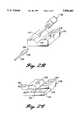
- FIG. 1is an isometric view of a micro-optical bench and molded device submount that comprise the subassembly according to the present invention
- FIGS. 2A-2Care isometric views of alternative embodiments of the micro-optical bench according to the present invention.
- FIGS. 3A-3Dillustrate an optical bench including a fiber stop for use with a "flip chip” optical detector, LED, or laser diode according to another aspect of the present invention.
- FIGS. 4A-4Dillustrate a hermetic package that is adaptable to mate with a variety of connector styles according to another aspect of the present invention.
- the present inventionis a passively aligned optical subassembly for use in a fiber-optic communication system.
- FIG. 1illustrates an optical subassembly according to the present invention.
- the subassembly 10generally comprises a micro-optical bench 12, an optical fiber 14 and a molded device submount 16.
- the purpose of the subassemblyis to secure a distal end 18 of the optical fiber 14 so that the distal end is positioned in front of an optical detector, LED, or laser diode 20 in a manner that maximizes the amount of light coupled between the optical fiber and the optical detector, LED, or laser diode.
- the micro-optical bench 12generally comprises a small wafer of semiconductor material such as silicon.
- the optical benchhas a length and width of 4 mm and a height of approximately 1 mm.
- On a top surface 22 of the micro-optical benchare three V-shaped grooves that are etched along a center line that extends between a front face 26 and a rear face 28 of the micro-optical bench 12.
- a soldering groove 30extends from the front face 26.
- a submount groove 32extends from the rear face 28 towards the front face 26. Connecting the soldering groove 30 and the submount groove 32 is a shallow fiber alignment groove 34.
- the soldering groove 30has a maximum width of approximately 0.6 mm and has a length of approximately 1 mm.
- the submount groove 32has a maximum width of approximately 1 mm and a length of approximately 2.3 mm.
- the fiber alignment groove 34has a width of approximately 0.3 mm and a length of 0.65 mm.
- Each of the grooves 30, 32, and 34may be either V-shaped or a truncated V shape, depending on when the etching process of the optical bench is halted. To reduce failure as a result of the stresses in the solder that occur at the point of the V-shaped groove with large variations in temperature, it is believed that a truncated soldering V-groove 30 is superior to the V-shaped soldering groove.
- Etched onto the top surface 22 of the micro-optical bench along either side of the submount groove 32are a plurality of vernier fiducials or accurately spaced markings 36 that allow a user to measure the distance between an optical detector, LED, or laser diode that is secured to the molded device submount 16 and the distal end 18 of the optical fiber 14.
- the walls and floor of the soldering groove 30are preferably metalized so that melted solder adheres to the soldering groove.
- the outer cladding 40 near the distal end of the optical fiberis also metalized.
- the distal end 18 of the fiberis laid in the fiber alignment groove 34 so that the metalized portion of the outer cladding 40 is positioned over the soldering groove 30.
- the optical bench 12 and a solder preformare heated so that the solder preform melts and secures the fiber in the soldering groove 30.
- the molded device submount 16comprises a generally rectangular piece of ceramic material.
- the submountpreferably has the same width, approximately 4 mm, as the optical bench 12 and a length of approximately 2 mm.
- the ridge 50Disposed on a bottom surface of the submount 16 is an outwardly extending ridge or nodule 50.
- the ridge 50has a semi-circular cross section and extends from a front face 52 of the submount to a rear face 54 of the submount.
- the radius of the ridge 50is sized such that it fits in the corresponding submount groove 32 that is disposed on the top surface of optical bench 12.
- the ridge 50operates to align the submount on the optical bench 12 so that the optical detector, LED, or laser diode 20 can be accurately positioned near the distal end 18 of the optical fiber 14.
- the device submount 16is preferably made of aluminum nitride if the optical detector, LED, or laser diode 20 generates heat and thermal conductivity is a consideration. If heat transfer is not a consideration, then the submount 16 is preferably made of aluminum oxide. To accurately control the radius of the ridge 50, an individual submount 16 is cut from a bar that is made according to the QuicksetTM process developed by Ceramics Process Systems. The QuicksetTM process is described in U.S. Pat. Nos. 4,816,182, 4,882,304, 4,904,411, 5,047,181, and 5,047,182.
- traces 60, 62Disposed on the top surface and the front face 52 of the submount 16 are a pair of traces 60, 62 that carry current to and from the optical detector, LED, or laser diode 20.
- the optical detector, LED, or laser diode 20is directly bonded to the trace 60, while a short bond wire 64 carries current from the optical detector, LED, or laser diode 20 to the second trace 62.
- a layer of adhesivesuch as epoxy, is placed on the bottom surface of the submount 16.
- the ridge of the submount 16is then placed in the submount groove 32 and aligned so that the optical detector, LED, or laser diode 20 is optimally positioned with respect to the distal end 18 of the optical fiber 14. Because the optical fiber is held in the alignment groove 34 and the device submount is held in the submount groove, the optical detector, LED, or laser diode 20 is transversely aligned with the distal end 18 of the optical fiber. To complete the alignment, it is only necessary to optimize the axial distance between the optical detector, LED, or laser diode and the distal end of the optical fiber.
- the axial alignment processis preferably done under a microscope or other magnification device using the vernier fiducials 36 described above.
- the epoxyis cured and the optical subassembly 10 is ready for incorporation into a hermetically sealed package.
- FIGS. 2A-2Cshow alternative embodiments of the micro-optical bench.
- An optical bench 80shown in FIG. 2A, is a silicon wafer having a submount groove 32 vernier fiducials 36 and a fiber alignment groove 34 similar to those found on the optical bench 12 shown in FIG. 1.
- the optical bench 80includes a step 84 that is cut or etched into a front face 86 of the bench.
- the step 84is generally defined by a riser 88 and a tread surface 90 that meets the riser 88.
- a soldering pad 92Disposed on the tread surface 90 that is centered underneath the fiber alignment groove 34.
- a solder preformis positioned on the solder pad 92 and a metalized portion of optical fiber is placed over the solder preform.
- the optical bench 80 and solder preformare then heated, thereby melting the solder onto the optical pad and surrounding the optical fiber. Because the solder only wets the area covered by the solder pad 92, the position of the optical fiber solder joint can be closely controlled.
- an optical submountfits within the submount groove 32 to align the optical detector, LED, or laser diode with a distal end of an optical fiber.
- FIG. 2Bshows another alternative embodiment of the micro-optical bench.
- the optical bench 110comprises a silicon wafer.
- a central groove 112Disposed on a top surface of the bench is a central groove 112 of substantially constant width and depth that extends from a front face 114 to a rear face 116 of the bench.
- a set of vernier fiducials 118is etched on either side of the central groove 112.
- an optical fiber 120is fitted through a cylindrical ferrule 122.
- the ferrule 122can be secured within the central groove 112 using an adhesive, such as epoxy.
- a distal end 124 of the optical fiberprotrudes through the end of the ferrule.
- a molded device submount 16 as shown in FIG. 1can be positioned in the central groove 112 to align an optical detector, LED, or laser diode with the optical fiber.
- a vertical cavity surface emitting laser (VCSEL) chip 130is shaped to fit the contours of the central groove 112.
- the VCSEL chip 130can be secured in the groove 112 with an epoxy or similar adhesive.
- the diameter of the cylindrical ferrule 122is selected such that the distal end 124 of the optical fiber aligns with the light emitting source of the VCSEL 130. Therefore, to construct the optical subassembly, it is only necessary to secure the ferrule 122 in the central groove 112 and to axially align the VCSEL chip 130 using the vernier fiducials 118 under a microscope before the adhesive is set.
- the VCSEL chipmay be bonded first, followed by the ferrule axial alignment and bonding.
- FIG. 2Cshows yet another alternative embodiment of the micro-optical bench.
- the micro-optical bench 150comprises a wafer of semiconductor material having a central groove 152 etched on the top surface of the bench.
- a step defined by a riser 154 and a tread surface 156is formed into the front face of the optical bench.
- the depth of the stepis equal to the depth of the central groove 152.
- a solder pad 160is placed on the tread surface 156 in front of the central groove 152.
- the optical fiber 120 including a cylindrical ferrule 122is positioned in the central groove 152.
- a portion of the optical fiber behind the ferruleis metalized and is secured to the solder pad 160 using a solder preform 162 that, when melted, secures the fiber to the solder pad 160.
- the optical bench 150can be used with either the VCSEL chip 130 shown in FIG. 2B or can accept the molded device submount 16 shown in FIG. 1.
- a set of vernier fiducials 164are etched in the upper surface of the optical bench 150 at a position on either side of the central groove 152.
- FIG. 3Ais a top plan view of a micro-optical bench 200 that is designed to be used with such a flip chip device.
- the bench 200again comprises a wafer of semiconductor material having a series of grooves etched in its top surface.
- a solder groove 210comprises a metalized truncated V-shaped groove that is sized to receive a metalized optical fiber in order to solder the fiber to the optical bench 200.
- solder groove 210At an end of the solder groove 210 is a narrower cladding groove 212 that is sized to receive the optical fiber, including the fiber's outer cladding layer. At the distal end of the cladding groove 212 is a still narrower core groove 214.
- FIG. 3Bshows in greater detail the cladding groove 212 and the core groove 214.
- the core groove 214has a width that is narrower than the cladding groove 212. The difference in widths and depths therefore creates a fiber stop 216 at the distal end of the cladding groove 212.
- a fiber 220comprises a cladding material 222 and an inner core 224. The distal end of the cladding material that surrounds the core will engage the fiber stop 216 to prevent the fiber from being further inserted into the cladding groove 212.
- the distal end of the core groove 214is angled and mirrored so that light from the core 224 is turned upward and delivered to the active element of the flip chipped device 240.
- FIG. 3Cshows the optical bench 200 with the fiber 220 installed.
- the optical fiber 220is secured in the solder groove 210 by heating the bench, and a solder preform until the preform melts and surrounds the fiber.
- a flip chip 240is positioned over the core groove 214 to transmit and receive light from the core.
- a pair of traces 242, 244are deposited on a top surface of the optical bench 200 to deliver current to and carry current from the flip chip device 240.
- FIG. 3Dis a cross-sectional view of the optical bench 200.
- the distance that the optical fiber is able to be inserted into the optical benchis controlled by the fiber stop 216 that abuts the distal end of the cladding material of the optical fiber 220.
- Light emitting from the fiberis reflected off the mirrored surface at the distal end of the core groove 214 where it is reflected upward as shown in FIG. 3D.
- device 240is an emitting device, light emitting from the flip-chipped LED or laser diode 240 will reflect off of the mirrored surface into the distal end of the fiber.
- the length of groove 214is designed to maximize the coupling of light from fiber 222 to device 240 and vice versa for light emitting device.
- the optical subassembly of the present inventionallows for the easy alignment because the optical fiber and the optical detector, LED, or laser diode are aligned by the grooves on the optical bench. Because these grooves transversely align the fiber and optical detector, LED, or laser diode, it is only necessary to adjust the axial distance between the end of the optical fiber and the optical detector, LED, or laser diode to complete the optical subassembly.
- a fiber stop incorporated in the optical subassemblyeliminates the need to adjust the axial position of the optical fiber.
- an optical subassemblyBefore an optical subassembly can be used in its intended environment, it must be hermetically sealed in a package.
- the packagingprevents moisture and dirt particles from contaminating the optical subassembly during its use.
- the problem with prior art subassembly packagingis that it is difficult to manufacture a package that is easily adapted to mate with a variety of fiber-optic connectors that are produced by different manufacturers. Therefore, in the past, it had been necessary to individually design each subassembly package for a particular type of connector. This process was labor-intensive and costly.
- the present inventionalso comprises a subassembly package that is more easily adapted to a variety of optical connector styles.
- FIG. 4Aillustrates a prior art optical subassembly package 300.
- the packagegenerally comprises a flat metal bed 302 with a front face 304, rear face 306, and a pair of sidewalls 305 that are bent at 90° to the plane of the bed.
- a printed circuit board 310including the optical subassembly, is mounted on the bed 302. Either an optical fiber is routed through an alignment ferrule, or a lens assembly 312 is mounted onto the front face 304 of the package.
- a cover 320is secured over the bed 302 and is hermetically sealed to complete the optical subassembly package.
- latching or connecting mechanism 322Most connectors that mate with the optical package 300 require some sort of latching or connecting mechanism 322 to be secured to the front face 304 of the optical package.
- the latching mechanisms 322are mounted on either side of the alignment ferrule or lens assembly 312. Because each manufacturer's specifications differ, it was previously necessary to retool the package in order to install the latching mechanisms for each connector type. In addition, because the front face of the package is relatively non-flat, small and thin, it was difficult to get the latching mechanisms to align properly with the alignment ferrule, lens assembly, and connector.
- the present inventionutilizes a faceplate that is secured to the front face 304 of the package.
- the faceplate 330comprises a flat, rectangular metal plate that is braised to the front face 304 of the package.
- a ferrule tube 316is braised in the center of the faceplate 330 in the center of the faceplate 330.
- the ferrule tubeis hollow and contains a slot 318 that is used for securing the fiber in the ferrule tube, as will be described below.
- the faceplate 330is flat and relatively thick, compared to the flatness and thickness of the front face 304 of the package, it is relatively easy to install an appropriate latching mechanisms on either side of the ferrule tube 316 that will mate with a variety of different connector types. Therefore, to produce optical packages for a variety of different connector types, it is only necessary to change the configuration of the particular faceplate that is mounted to the front face of the package.
- a cylindrical ferrule 352is inserted into the ferrule tube 316.
- the outer diameter of the ferrule 352is slightly greater than the inner diameter of the ferrule tube 316.
- the optical fiber 350is inserted into the ferrule 352 from the inside of the package 300.
- the fiberis hermetically sealed in the package with solder.
- An epoxy or other adhesivecan then be used to secure the fiber in the ferrule tube 316 by delivering the epoxy through the slot 318 that is cut in the side of the ferrule tube 316. Once the epoxy is set, the fiber and any portion of the ferrule that extends from the end of the ferrule tube can be cut and polished, if desired.
- FIG. 4Cis a side, cross-sectional view of the hermetic package including the faceplate 330 according to the present invention.
- the end of the fiberis cut and the portion of the optical fiber and ferrule protruding from the distal end of the ferrule tube 316 is polished to mate with an appropriate connector.
- a length of optical fiber extending from the hermetic packagein order to either launch light into the package or to monitor the light output from the package during assembly of the optoelectronic circuit inside the package.
- a length of optic fiber 350extends from the distal end of the ferrule 352 for subsequent connection to a length of fiber-optic cable.
- an optical benchmay include more than one optical detector, LED, or laser diode mounted in any of the ways specified above. Therefore, the scope of the invention is to be determined solely from the following claims and equivalents thereto.
Landscapes
- Physics & Mathematics (AREA)
- General Physics & Mathematics (AREA)
- Optics & Photonics (AREA)
- Optical Couplings Of Light Guides (AREA)
- Semiconductor Lasers (AREA)
Abstract
Description
The U.S. Government has a paid-up license in this invention and the right in limited circumstances to require the patent owner to license others on reasonable terms as provided by the terms of Wright Lab F33615-94-C-1483 awarded by DARPA.
The present invention relates to the alignment of an optical fiber in a fiber-optic transmitter/receiver subassembly.
The manufacture of optoelectronic modules, such as optoelectronic receivers and optoelectronic transmitters, requires that an optical fiber be properly aligned and fixed in an optical subassembly. In an optical receiver, a fiber is aligned with an optical detector, usually a PIN photodiode. In an optical transmitter, an optical fiber is aligned with a light-emitting diode (LED) or a laser diode. A goal of optical alignment is to maximize the amount of light coupling between the optical detector, LED, or laser diode and the optical fiber. The alignment of the fiber member with the LED, laser diode, or optical detector is a critical step in the manufacture of an optoelectronic subassembly.
In the past, the step of aligning an optical fiber had to be done actively. Typically, the process involves fixing the position of either the optical detector, LED, or laser diode or the optical fiber, and positioning the freely moving fiber or optical detector, LED, or laser diode while simultaneously measuring the amount of light coupled between the two so that a maximum amount of light is passed. Once the optimum position is found, the position of the optical fiber or optical detector, LED, or laser diode is fixed. While this process generally works well, it is both labor-intensive and costly.
Optical subassemblies are often used in harsh environments where they are subjected to wide variations in temperature, pressure, and g-forces. To withstand such environments, such subassemblies are often mounted in hermetically sealed packages. Each package is adapted to mate with a connector that contains an optical fiber. Typically, the connectors made by each manufacturer require a different type of latching mechanism to be mounted to the package. In addition to the problem of aligning the optical fiber with the optical detector, LED, or laser diode, it has also been difficult to produce a subassembly package that can be easily adapted to mate with a variety of optical connectors made by different manufacturers.
Given the shortcoming in the prior art, there is a need for a method of producing optical subassemblies in a cost-effective manner that does not require active alignment of an optical fiber with an optical detector, LED, or laser diode. In addition, there is a need for a subassembly package that is easily adapted to mate with a variety of connector types.
The present invention comprises an optical subassembly including an optical bench and molded device submount. The optical bench is a wafer of semiconductor material having a plurality of grooves etched in a top surface thereof. The grooves include a submount groove that is adapted to receive a ridge or nodule formed on a bottom surface of a molded device submount. Mounted on the submount is an optical detector, LED, or laser diode. When placed on the optical bench, the ridge or nodule of the device submount fits within the submount groove in order to transversely align the optical detector, LED, or laser diode with an end of an optical fiber. Alternatively, the optical detector, LED, or laser diode may be directly bonded within a groove disposed on a top surface of the optical bench. The optical fiber may be aligned and secured to the optical bench in a variety of ways. For example, a solder groove can be etched into the bench and the fiber then soldered in the solder groove to secure the fiber to the bench. Alternatively, the optical fiber can be soldered to a step that is cut or etched into the top surface of the optical bench. Finally, a ferrule can be placed over the optical fiber and can be adhesively secured in a groove disposed on the top surface of the optical bench.
The invention also comprises a subassembly package that can be adapted to mate with a plurality of different connector styles. The package includes a faceplate that is secured to a front face of the package. The faceplate provides a flat, relatively stiff surface on which a variety of latching mechanisms can be easily mounted in order to allow the package to mate with different connector types.
The foregoing aspects and many of the attendant advantages of this invention will become more readily appreciated as the same becomes better understood by reference to the following detailed description, when taken in conjunction with the accompanying drawings, wherein:
FIG. 1 is an isometric view of a micro-optical bench and molded device submount that comprise the subassembly according to the present invention;
FIGS. 2A-2C are isometric views of alternative embodiments of the micro-optical bench according to the present invention;
FIGS. 3A-3D illustrate an optical bench including a fiber stop for use with a "flip chip" optical detector, LED, or laser diode according to another aspect of the present invention; and
FIGS. 4A-4D illustrate a hermetic package that is adaptable to mate with a variety of connector styles according to another aspect of the present invention.
The present invention is a passively aligned optical subassembly for use in a fiber-optic communication system.
FIG. 1 illustrates an optical subassembly according to the present invention. Thesubassembly 10 generally comprises amicro-optical bench 12, anoptical fiber 14 and a moldeddevice submount 16. The purpose of the subassembly is to secure adistal end 18 of theoptical fiber 14 so that the distal end is positioned in front of an optical detector, LED, orlaser diode 20 in a manner that maximizes the amount of light coupled between the optical fiber and the optical detector, LED, or laser diode.
Themicro-optical bench 12 generally comprises a small wafer of semiconductor material such as silicon. In the presently preferred embodiment of the invention, the optical bench has a length and width of 4 mm and a height of approximately 1 mm. On atop surface 22 of the micro-optical bench are three V-shaped grooves that are etched along a center line that extends between afront face 26 and arear face 28 of themicro-optical bench 12. Asoldering groove 30 extends from thefront face 26. Asubmount groove 32 extends from therear face 28 towards thefront face 26. Connecting the solderinggroove 30 and thesubmount groove 32 is a shallowfiber alignment groove 34.
In the presently preferred embodiment of the invention, thesoldering groove 30 has a maximum width of approximately 0.6 mm and has a length of approximately 1 mm. Thesubmount groove 32 has a maximum width of approximately 1 mm and a length of approximately 2.3 mm. Finally, thefiber alignment groove 34 has a width of approximately 0.3 mm and a length of 0.65 mm. Each of thegrooves groove 30 is superior to the V-shaped soldering groove.
Etched onto thetop surface 22 of the micro-optical bench along either side of thesubmount groove 32 are a plurality of vernier fiducials or accurately spacedmarkings 36 that allow a user to measure the distance between an optical detector, LED, or laser diode that is secured to the moldeddevice submount 16 and thedistal end 18 of theoptical fiber 14.
The walls and floor of the solderinggroove 30 are preferably metalized so that melted solder adheres to the soldering groove. To align and secure theoptical fiber 14 to theoptical bench 12, theouter cladding 40 near the distal end of the optical fiber is also metalized. Thedistal end 18 of the fiber is laid in thefiber alignment groove 34 so that the metalized portion of theouter cladding 40 is positioned over thesoldering groove 30. Theoptical bench 12 and a solder preform are heated so that the solder preform melts and secures the fiber in thesoldering groove 30.
The moldeddevice submount 16 comprises a generally rectangular piece of ceramic material. The submount preferably has the same width, approximately 4 mm, as theoptical bench 12 and a length of approximately 2 mm.
Disposed on a bottom surface of thesubmount 16 is an outwardly extending ridge ornodule 50. In the presently preferred embodiment of the invention, theridge 50 has a semi-circular cross section and extends from afront face 52 of the submount to arear face 54 of the submount. The radius of theridge 50 is sized such that it fits in thecorresponding submount groove 32 that is disposed on the top surface ofoptical bench 12. Theridge 50 operates to align the submount on theoptical bench 12 so that the optical detector, LED, orlaser diode 20 can be accurately positioned near thedistal end 18 of theoptical fiber 14.
Thedevice submount 16 is preferably made of aluminum nitride if the optical detector, LED, orlaser diode 20 generates heat and thermal conductivity is a consideration. If heat transfer is not a consideration, then thesubmount 16 is preferably made of aluminum oxide. To accurately control the radius of theridge 50, anindividual submount 16 is cut from a bar that is made according to the Quickset™ process developed by Ceramics Process Systems. The Quickset™ process is described in U.S. Pat. Nos. 4,816,182, 4,882,304, 4,904,411, 5,047,181, and 5,047,182.
Disposed on the top surface and thefront face 52 of thesubmount 16 are a pair oftraces laser diode 20. The optical detector, LED, orlaser diode 20 is directly bonded to thetrace 60, while ashort bond wire 64 carries current from the optical detector, LED, orlaser diode 20 to thesecond trace 62.
To secure thesubmount 16 to theoptical bench 12, a layer of adhesive, such as epoxy, is placed on the bottom surface of thesubmount 16. The ridge of thesubmount 16 is then placed in thesubmount groove 32 and aligned so that the optical detector, LED, orlaser diode 20 is optimally positioned with respect to thedistal end 18 of theoptical fiber 14. Because the optical fiber is held in thealignment groove 34 and the device submount is held in the submount groove, the optical detector, LED, orlaser diode 20 is transversely aligned with thedistal end 18 of the optical fiber. To complete the alignment, it is only necessary to optimize the axial distance between the optical detector, LED, or laser diode and the distal end of the optical fiber. The axial alignment process is preferably done under a microscope or other magnification device using the vernier fiducials 36 described above. Once the submount is positioned in the submount groove, the epoxy is cured and theoptical subassembly 10 is ready for incorporation into a hermetically sealed package. Alternatively, one may secure the submount to the optical bench before axially aligning and soldering the optical fiber to the optical bench.
FIGS. 2A-2C show alternative embodiments of the micro-optical bench. Anoptical bench 80, shown in FIG. 2A, is a silicon wafer having asubmount groove 32vernier fiducials 36 and afiber alignment groove 34 similar to those found on theoptical bench 12 shown in FIG. 1. Instead of thesoldering groove 30, theoptical bench 80 includes astep 84 that is cut or etched into afront face 86 of the bench. Thestep 84 is generally defined by ariser 88 and atread surface 90 that meets theriser 88. Disposed on thetread surface 90 is asoldering pad 92 that is centered underneath thefiber alignment groove 34.
To secure the optical fiber on theoptical bench 80, a solder preform is positioned on thesolder pad 92 and a metalized portion of optical fiber is placed over the solder preform. Theoptical bench 80 and solder preform are then heated, thereby melting the solder onto the optical pad and surrounding the optical fiber. Because the solder only wets the area covered by thesolder pad 92, the position of the optical fiber solder joint can be closely controlled. As with the previous embodiment shown in FIG. 1, an optical submount fits within thesubmount groove 32 to align the optical detector, LED, or laser diode with a distal end of an optical fiber.
FIG. 2B shows another alternative embodiment of the micro-optical bench. Theoptical bench 110 comprises a silicon wafer. Disposed on a top surface of the bench is acentral groove 112 of substantially constant width and depth that extends from afront face 114 to arear face 116 of the bench. A set ofvernier fiducials 118 is etched on either side of thecentral groove 112. To secure an optical fiber in thecentral groove 112, anoptical fiber 120 is fitted through acylindrical ferrule 122. Theferrule 122 can be secured within thecentral groove 112 using an adhesive, such as epoxy. Adistal end 124 of the optical fiber protrudes through the end of the ferrule. Provided that no more than approximately 0.050 inch of optical fiber extends through the ferrule, the ferrule will hold the distal end of the fiber in the proper position with respect to an optical detector, LED, or laser diode. A moldeddevice submount 16 as shown in FIG. 1 can be positioned in thecentral groove 112 to align an optical detector, LED, or laser diode with the optical fiber.
As an alternative to mounting the laser diode on a molded device submount, a vertical cavity surface emitting laser (VCSEL)chip 130 is shaped to fit the contours of thecentral groove 112. TheVCSEL chip 130 can be secured in thegroove 112 with an epoxy or similar adhesive. The diameter of thecylindrical ferrule 122 is selected such that thedistal end 124 of the optical fiber aligns with the light emitting source of theVCSEL 130. Therefore, to construct the optical subassembly, it is only necessary to secure theferrule 122 in thecentral groove 112 and to axially align theVCSEL chip 130 using the vernier fiducials 118 under a microscope before the adhesive is set. Alternatively, the VCSEL chip may be bonded first, followed by the ferrule axial alignment and bonding.
FIG. 2C shows yet another alternative embodiment of the micro-optical bench. Themicro-optical bench 150 comprises a wafer of semiconductor material having acentral groove 152 etched on the top surface of the bench. A step defined by ariser 154 and atread surface 156 is formed into the front face of the optical bench. Preferably, the depth of the step is equal to the depth of thecentral groove 152. Asolder pad 160 is placed on thetread surface 156 in front of thecentral groove 152.
Theoptical fiber 120 including acylindrical ferrule 122 is positioned in thecentral groove 152. However, in this embodiment, a portion of the optical fiber behind the ferrule is metalized and is secured to thesolder pad 160 using asolder preform 162 that, when melted, secures the fiber to thesolder pad 160. Theoptical bench 150 can be used with either theVCSEL chip 130 shown in FIG. 2B or can accept the moldeddevice submount 16 shown in FIG. 1. A set ofvernier fiducials 164 are etched in the upper surface of theoptical bench 150 at a position on either side of thecentral groove 152. To align the optical detector, LED, or laser diode with adistal end 124 of the optical fiber, it is only necessary to closely measure the distance between the distal end of the fiber and the optical detector, LED, or laser diode using the vernier fiducials.
In some instances, it is necessary to use the optical bench with a so-called "flip chip" that has the active optical detector, LED, or laser diode element oriented in a direction that is normal to the top surface of the optical bench. FIG. 3A is a top plan view of amicro-optical bench 200 that is designed to be used with such a flip chip device. Thebench 200 again comprises a wafer of semiconductor material having a series of grooves etched in its top surface. Asolder groove 210 comprises a metalized truncated V-shaped groove that is sized to receive a metalized optical fiber in order to solder the fiber to theoptical bench 200. At an end of thesolder groove 210 is anarrower cladding groove 212 that is sized to receive the optical fiber, including the fiber's outer cladding layer. At the distal end of thecladding groove 212 is a stillnarrower core groove 214.
FIG. 3B shows in greater detail thecladding groove 212 and thecore groove 214. As can be seen, thecore groove 214 has a width that is narrower than thecladding groove 212. The difference in widths and depths therefore creates afiber stop 216 at the distal end of thecladding groove 212. Afiber 220 comprises acladding material 222 and aninner core 224. The distal end of the cladding material that surrounds the core will engage thefiber stop 216 to prevent the fiber from being further inserted into thecladding groove 212. The distal end of thecore groove 214 is angled and mirrored so that light from thecore 224 is turned upward and delivered to the active element of the flip chippeddevice 240.
FIG. 3C shows theoptical bench 200 with thefiber 220 installed. Theoptical fiber 220 is secured in thesolder groove 210 by heating the bench, and a solder preform until the preform melts and surrounds the fiber. Aflip chip 240 is positioned over thecore groove 214 to transmit and receive light from the core. A pair oftraces optical bench 200 to deliver current to and carry current from theflip chip device 240.
FIG. 3D is a cross-sectional view of theoptical bench 200. As indicated above, the distance that the optical fiber is able to be inserted into the optical bench is controlled by thefiber stop 216 that abuts the distal end of the cladding material of theoptical fiber 220. Light emitting from the fiber is reflected off the mirrored surface at the distal end of thecore groove 214 where it is reflected upward as shown in FIG. 3D. Ifdevice 240 is an emitting device, light emitting from the flip-chipped LED orlaser diode 240 will reflect off of the mirrored surface into the distal end of the fiber. The length ofgroove 214 is designed to maximize the coupling of light fromfiber 222 todevice 240 and vice versa for light emitting device.
As will be appreciated, the optical subassembly of the present invention allows for the easy alignment because the optical fiber and the optical detector, LED, or laser diode are aligned by the grooves on the optical bench. Because these grooves transversely align the fiber and optical detector, LED, or laser diode, it is only necessary to adjust the axial distance between the end of the optical fiber and the optical detector, LED, or laser diode to complete the optical subassembly. A fiber stop incorporated in the optical subassembly eliminates the need to adjust the axial position of the optical fiber.
Before an optical subassembly can be used in its intended environment, it must be hermetically sealed in a package. The packaging prevents moisture and dirt particles from contaminating the optical subassembly during its use. As indicated above, the problem with prior art subassembly packaging is that it is difficult to manufacture a package that is easily adapted to mate with a variety of fiber-optic connectors that are produced by different manufacturers. Therefore, in the past, it had been necessary to individually design each subassembly package for a particular type of connector. This process was labor-intensive and costly.
To reduce the need for having to fit each individual optical subassembly package to a particular type of connector, the present invention also comprises a subassembly package that is more easily adapted to a variety of optical connector styles.
FIG. 4A illustrates a prior artoptical subassembly package 300. The package generally comprises aflat metal bed 302 with afront face 304,rear face 306, and a pair ofsidewalls 305 that are bent at 90° to the plane of the bed. A printedcircuit board 310, including the optical subassembly, is mounted on thebed 302. Either an optical fiber is routed through an alignment ferrule, or alens assembly 312 is mounted onto thefront face 304 of the package. Acover 320 is secured over thebed 302 and is hermetically sealed to complete the optical subassembly package.
Most connectors that mate with theoptical package 300 require some sort of latching or connectingmechanism 322 to be secured to thefront face 304 of the optical package. Typically the latchingmechanisms 322 are mounted on either side of the alignment ferrule orlens assembly 312. Because each manufacturer's specifications differ, it was previously necessary to retool the package in order to install the latching mechanisms for each connector type. In addition, because the front face of the package is relatively non-flat, small and thin, it was difficult to get the latching mechanisms to align properly with the alignment ferrule, lens assembly, and connector.
To eliminate the need to individually tool the package for a particular type of connector, the present invention utilizes a faceplate that is secured to thefront face 304 of the package. As shown in FIG. 4B, thefaceplate 330 comprises a flat, rectangular metal plate that is braised to thefront face 304 of the package. In the center of thefaceplate 330 is a hole in which aferrule tube 316 is braised. The ferrule tube is hollow and contains aslot 318 that is used for securing the fiber in the ferrule tube, as will be described below. Because thefaceplate 330 is flat and relatively thick, compared to the flatness and thickness of thefront face 304 of the package, it is relatively easy to install an appropriate latching mechanisms on either side of theferrule tube 316 that will mate with a variety of different connector types. Therefore, to produce optical packages for a variety of different connector types, it is only necessary to change the configuration of the particular faceplate that is mounted to the front face of the package.
To secure anoptical fiber 350 within theferrule tube 316, acylindrical ferrule 352 is inserted into theferrule tube 316. Preferably, the outer diameter of theferrule 352 is slightly greater than the inner diameter of theferrule tube 316. Theoptical fiber 350 is inserted into theferrule 352 from the inside of thepackage 300. The fiber is hermetically sealed in the package with solder. An epoxy or other adhesive can then be used to secure the fiber in theferrule tube 316 by delivering the epoxy through theslot 318 that is cut in the side of theferrule tube 316. Once the epoxy is set, the fiber and any portion of the ferrule that extends from the end of the ferrule tube can be cut and polished, if desired.
FIG. 4C is a side, cross-sectional view of the hermetic package including thefaceplate 330 according to the present invention. In this embodiment, the end of the fiber is cut and the portion of the optical fiber and ferrule protruding from the distal end of theferrule tube 316 is polished to mate with an appropriate connector.
In some instances, it is desirable to leave a length of optical fiber extending from the hermetic package in order to either launch light into the package or to monitor the light output from the package during assembly of the optoelectronic circuit inside the package. As shown in FIG. 4D, a length ofoptic fiber 350 extends from the distal end of theferrule 352 for subsequent connection to a length of fiber-optic cable.
By using thefaceplate 330, it is easy to install the latching mechanisms that will mate with a variety of connector types without having to individually machine each optical package.
While the preferred embodiment of the invention has been illustrated and described, it will be appreciated that various changes can be made therein without departing from the spirit and scope of the invention. For example, an optical bench may include more than one optical detector, LED, or laser diode mounted in any of the ways specified above. Therefore, the scope of the invention is to be determined solely from the following claims and equivalents thereto.
Claims (13)
1. An optical subassembly for aligning a distal end of an optical fiber with an optical detector, LED, or laser diode, comprising:
an optical bench having a submount groove disposed on a top surface thereof and means for securing the optical fiber to the optical bench,
a submount having an optical detector, LED, or laser diode mounted thereon, the submount cooperating with the submount groove to transversely align the optical detector, LED, or laser diode with the distal end of the optical fiber; and
a ridge disposed on a bottom surface of the submount, the ridge fitting within the submount groove on the optical bench.
2. An optical subassembly for aligning a distal end of an optical fiber with an optical detector, LED, or laser diode, comprising:
an optical bench having a submount groove disposed on a top surface thereof;
a submount having an optical detector, LED, or laser diode mounted thereon, the submount cooperating with the submount groove to transversely align the optical detector, LED, or laser diode with the distal end of the optical fiber; and
a truncated metalized soldering groove disposed on the top surface of the optical bench into which a portion of the optical fiber is secured.
3. The optical subassembly of claim 2, further comprising an alignment groove in which the optical fiber is seated, wherein the alignment groove is smaller in width than the submount groove.
4. An optical subassembly for aligning a distal end of an optical fiber with an optical detector, LED, or laser diode, comprising:
an optical bench having a submount groove disposed on a top surface thereof;
a submount having an optical detector, LED, or laser diode mounted thereon, the submount cooperating with the submount groove to transversely align the optical detector, LED, or laser diode with the distal end of the optical fiber; and
a step that is etched into the top surface of the optical bench, the step including a solder pad to which a portion of the optical fiber is secured.
5. An optical bench for aligning a distal end of an optical fiber with an optical detector, LED, or laser diode, comprising:
a semiconductor wafer having a plurality of channels etched into a top surface thereof the channels including a first channel having a width and depth selected to receive a cladding and core of the optical fiber and a second channel having a width that is narrower than the width of the first channel, the first and second channels being aligned such that a fiber stop is created at a point where the first and second channels meet, the fiber stop engaging the cladding of the optical fiber to control the axial position at which the fiber is positioned in the channels,
wherein an end of the second channel is mirrored to change the direction of light upward the optical fiber.
6. A hermetically sealed optical subassembly housing a bed having a front face, a rear face, and sidewalls wherein the bed is adapted to secure an optical subassembly, comprising:
a faceplate secured to the front face of the bed, the faceplate having one or more hollow ferrule tubes secured thereto, said ferrule tubes each having an optical fiber disposed therein; and
a cover that fits over the bed.
7. The hermetically sealed subassembly housing of claim 6, further comprising:
a ferrule that fits over each optical fiber and in each ferrule tube in order to secure the optical fiber in the ferrule.
8. The hermetically sealed optical subassembly housing of claim 6, wherein the fiber is hermetically sealed in the ferrule tube with solder and secured in the ferrule tube with an adhesive.
9. The hermetically sealed optical subassembly housing of claim 6, wherein the faceplate includes a latching mechanism that mates with a corresponding optical connector.
10. An optical subassembly for aligning a distal end of an optical fiber with a vertical cavity surface emitting laser (VCSEL) chip, comprising:
an optical bench having a singular uniform groove disposed on a top surface thereof;
a VCSEL chip mounted in the groove;
an optical fiber mounted in the groove;
a ferrule around the optical fiber; and
a step that is etched into the top surface of the optical bench, the step including a solder pad to which the optical fiber is secured.
11. An optical subassembly for aligning a distal end of an optical fiber with an optical detector, LED, or laser diode, comprising:
an optical bench having a submount groove disposed on a top surface thereof and a step that is etched into the top surface of the optical bench, the step including a solder pad to which a portion of the optical fiber is secured such that the distal end of the optical fiber is aligned with the submount groove; and
a submount having an optical detector, LED, or laser diode mounted thereon, the submount cooperating with the submount groove to transversely align the optical detector, LED, or laser diode with the distal end of the optical fiber.
12. The optical subassembly of claim 11, wherein the submount further comprises a ridge disposed on a bottom surface of the submount, the ridge fitting within the submount groove on the optical bench.
13. An optical subassembly for aligning a distal end of an optical fiber with an optical detector, LED, or laser diode, comprising:
an optical bench having a groove disposed on a top surface thereof and a step that is etched into the top surface of the optical bench, the step including a solder pad to which a portion of the optical fiber is secured such that the distal end of the optical fiber is aligned with the groove; and
an optical detector, LED, or laser diode mounted in the groove.
Priority Applications (1)
| Application Number | Priority Date | Filing Date | Title |
|---|---|---|---|
| US08/866,891US5896481A (en) | 1997-05-30 | 1997-05-30 | Optical subassembly with a groove for aligning an optical device with an optical fiber |
Applications Claiming Priority (1)
| Application Number | Priority Date | Filing Date | Title |
|---|---|---|---|
| US08/866,891US5896481A (en) | 1997-05-30 | 1997-05-30 | Optical subassembly with a groove for aligning an optical device with an optical fiber |
Publications (1)
| Publication Number | Publication Date |
|---|---|
| US5896481Atrue US5896481A (en) | 1999-04-20 |
Family
ID=25348659
Family Applications (1)
| Application Number | Title | Priority Date | Filing Date |
|---|---|---|---|
| US08/866,891Expired - LifetimeUS5896481A (en) | 1997-05-30 | 1997-05-30 | Optical subassembly with a groove for aligning an optical device with an optical fiber |
Country Status (1)
| Country | Link |
|---|---|
| US (1) | US5896481A (en) |
Cited By (66)
| Publication number | Priority date | Publication date | Assignee | Title |
|---|---|---|---|---|
| US6164837A (en)* | 1998-12-30 | 2000-12-26 | Mcdonnell Douglas Corporation | Integrated microelectromechanical alignment and locking apparatus and method for fiber optic module manufacturing |
| EP0987769A3 (en)* | 1998-09-18 | 2001-03-07 | Sumitomo Electric Industries, Ltd. | Photodiode module |
| WO2001026190A1 (en)* | 1999-10-07 | 2001-04-12 | New Focus, Inc. | Assembly and associated method for supportively affixing an object upon a substrate |
| US6216939B1 (en)* | 1998-12-31 | 2001-04-17 | Jds Uniphase Photonics C.V. | Method for making a hermetically sealed package comprising at least one optical fiber feedthrough |
| US6217233B1 (en)* | 1998-12-11 | 2001-04-17 | At&T Corporation | Restoration splice method and apparatus |
| US6289031B1 (en)* | 1999-05-14 | 2001-09-11 | Raytheon Company | Integrated lightweight optical bench and miniaturized laser transmitter using same |
| WO2002037154A1 (en)* | 2000-11-06 | 2002-05-10 | Mitsubishi Chemical Corporation | Structure for adjusting position of optical fiber and semiconductor laser module |
| US20020090013A1 (en)* | 2001-01-09 | 2002-07-11 | Murry Stefan J. | VCSEL assembly with edge-receiving optical devices |
| US20020195417A1 (en)* | 2001-04-20 | 2002-12-26 | Steinberg Dan A. | Wet and dry etching process on <110> silicon and resulting structures |
| US20030021572A1 (en)* | 2001-02-07 | 2003-01-30 | Steinberg Dan A. | V-groove with tapered depth and method for making |
| US20030020130A1 (en)* | 2001-02-07 | 2003-01-30 | Steinberg Dan A. | Combined wet and dry etching process for micromachining of crystalline materials |
| US20030044134A1 (en)* | 2001-08-31 | 2003-03-06 | Strachan William J. | Optical sub-assembly package |
| EP1046938A3 (en)* | 1999-04-23 | 2003-03-12 | Sick AG | Connection device |
| US20030059622A1 (en)* | 2001-02-14 | 2003-03-27 | Steinberg Dan A. | Micromachined structures made by combined wet and dry etching |
| US20030067049A1 (en)* | 2001-02-07 | 2003-04-10 | Steinberg Dan A. | Etching process for micromachining crystalline materials and devices fabricated thereby |
| US20030075355A1 (en)* | 2000-12-26 | 2003-04-24 | Anderson Gene R. | An apparatus and method of using flexible printed circuit board in optical transceiver device |
| US20030118310A1 (en)* | 2000-10-26 | 2003-06-26 | Steinberg Dan A. | Variable width waveguide for mode-matching and method for making |
| US6597843B2 (en) | 2001-07-10 | 2003-07-22 | International Business Machines Corporation | Fiber pivot for optical alignment |
| US6627096B2 (en) | 2000-05-02 | 2003-09-30 | Shipley Company, L.L.C. | Single mask technique for making positive and negative micromachined features on a substrate |
| US20030223700A1 (en)* | 2002-06-04 | 2003-12-04 | Fiberlead, Inc. | Optical fiber array connector |
| US20030234403A1 (en)* | 2002-06-20 | 2003-12-25 | Chung-Shin Mou | Optical package structure |
| US20040062484A1 (en)* | 2002-08-29 | 2004-04-01 | International Business Machines Corporation | Self-aligned optical waveguide to optical fiber connection system |
| WO2004038473A1 (en)* | 2002-10-22 | 2004-05-06 | Firecomms Limited | Connection of optical waveguides to optical devices |
| US6754427B2 (en)* | 2001-02-08 | 2004-06-22 | Shipley Company, L.L.C. | Method and device passively locating a fiber stub in a groove |
| US20040146253A1 (en)* | 2003-01-28 | 2004-07-29 | Wang Charlie X. | Method and apparatus for parallel optical transceiver module assembly |
| US6799902B2 (en) | 2000-12-26 | 2004-10-05 | Emcore Corporation | Optoelectronic mounting structure |
| US20040204213A1 (en)* | 2003-04-10 | 2004-10-14 | David Schugar | Wagering method, device, and computer readable storage medium, for wagering on pieces in a progression |
| US6811853B1 (en) | 2000-03-06 | 2004-11-02 | Shipley Company, L.L.C. | Single mask lithographic process for patterning multiple types of surface features |
| US20040264886A1 (en)* | 2003-06-26 | 2004-12-30 | Michael Powers | Low cost package design for fiber coupled optical component |
| US20050013555A1 (en)* | 2003-06-11 | 2005-01-20 | Mitsuaki Nishie | Optical module and mounting component |
| US20050018972A1 (en)* | 2000-12-26 | 2005-01-27 | Anderson Gene R. | Housing and mounting structure |
| US20050051598A1 (en)* | 2003-09-05 | 2005-03-10 | Trebor Heminway | Solder preform for low heat stress laser solder attachment |
| US6905252B2 (en) | 2002-08-21 | 2005-06-14 | Finisar Corporation | Optical interconnection sub-assembly |
| US6905260B2 (en) | 2000-12-26 | 2005-06-14 | Emcore Corporation | Method and apparatus for coupling optical elements to optoelectronic devices for manufacturing optical transceiver modules |
| US20050135775A1 (en)* | 2003-12-19 | 2005-06-23 | Industrial Technology Research Institute | Assembly apparatus for an optical transceiver |
| US6917056B2 (en) | 2001-01-31 | 2005-07-12 | Shipley Company, L.L.C. | Optoelectronic submount having an on-edge optoelectronic device |
| US20050175296A1 (en)* | 2004-02-06 | 2005-08-11 | Brian Massey | Diamond 2D scan for aligning an optical fiber to an optical output port |
| US20050226569A1 (en)* | 2002-11-13 | 2005-10-13 | Nobuo Sashinaka | Optical communications module and substrate for the same |
| US20050259943A1 (en)* | 2002-10-17 | 2005-11-24 | Sigmund Braun | Electric tool |
| US20050274959A1 (en)* | 2004-06-10 | 2005-12-15 | Geun-Ho Kim | High power LED package |
| US20050281515A1 (en)* | 2004-05-10 | 2005-12-22 | Chris Togami | Aligning optical components with three degrees of translational freedom |
| US7021836B2 (en) | 2000-12-26 | 2006-04-04 | Emcore Corporation | Attenuator and conditioner |
| US7021838B2 (en) | 2003-12-16 | 2006-04-04 | Matsushita Electric Industrial Co., Ltd. | Optimizing alignment of an optical fiber to an optical output port |
| US20060204177A1 (en)* | 2005-03-14 | 2006-09-14 | Matsushita Electric Industrial Co., Ltd. | Low cost, high precision multi-point optical component attachment |
| US7124928B2 (en)* | 2001-01-16 | 2006-10-24 | Axsun Technologies, Inc. | Optical component installation and train alignment process utilizing metrology and plastic deformation |
| US7157016B2 (en) | 2003-05-23 | 2007-01-02 | Rohm And Haas Electronic Materials Llc | Etching process for micromachining crystalline materials and devices fabricated thereby |
| US20070019899A1 (en)* | 2005-07-25 | 2007-01-25 | Fuji Xerox Co., Ltd. | Sub-mount for mounting optical component, manufacturing method thereof, and light transmission and reception module |
| US7284913B2 (en) | 2003-07-14 | 2007-10-23 | Matsushita Electric Industrial Co., Ltd. | Integrated fiber attach pad for optical package |
| US20080101752A1 (en)* | 2006-11-01 | 2008-05-01 | Chan Eric Y | Small-form-factor fiber optic transceiver module having built-in test capability and method |
| US20090257716A1 (en)* | 2008-04-11 | 2009-10-15 | Chan Eric Y | Optical star coupler |
| US20100310214A1 (en)* | 2007-11-15 | 2010-12-09 | Nobuo Miyadera | Optical connecting structure |
| USRE43542E1 (en) | 2000-06-12 | 2012-07-24 | Adc Gmbh | Assembly and method for use in terminating an optical fiber or fibers |
| WO2012176409A1 (en)* | 2011-06-22 | 2012-12-27 | パナソニック株式会社 | Optical module |
| US20130004118A1 (en)* | 2011-06-29 | 2013-01-03 | Tyco Electronics Corporation | Optical interposer with common angled surface |
| US20130129276A1 (en)* | 2011-11-18 | 2013-05-23 | Universal Microelectronics Co., Ltd. | Optical engine assembly and optoelectronic package |
| US20140126861A1 (en)* | 2012-11-08 | 2014-05-08 | Hon Hai Precision Industry Co., Ltd. | Fixing device for optical fiber detection |
| US20160070083A1 (en)* | 2013-05-10 | 2016-03-10 | M Squared Lasers Limited | Method and apparatus for mounting optical components |
| US10139567B1 (en)* | 2017-10-10 | 2018-11-27 | The United States Of America As Represented By The Secretary Of The Navy | Dematable expanded beam fiber optic connector |
| US10209477B1 (en)* | 2017-05-25 | 2019-02-19 | Lockheed Martin Coherent Technologies, Inc. | Systems and methods for reconfigurable micro-optic assemblies |
| CN110998401A (en)* | 2017-06-01 | 2020-04-10 | 菲尼萨公司 | Connector assembly for optoelectronic module |
| US20210072471A1 (en)* | 2012-03-05 | 2021-03-11 | Cudoquanta Florida, Inc. | Hermetic optical fiber alignment assembly having integrated optical element |
| US20220096677A1 (en)* | 2020-09-28 | 2022-03-31 | The Boeing Company | Optical Disinfection Systems Having Side-Emitting Optical Fiber Coupled to High-Energy UV-C Laser Diode |
| US20220123522A1 (en)* | 2019-03-01 | 2022-04-21 | Shenzhen Raysees Technology Co., Ltd. | Pattern projector based on vertical cavity surface emitting laser (vcsel) array |
| TWI764505B (en)* | 2021-01-11 | 2022-05-11 | 香港商雲暉科技有限公司 | Fiber end fixing structure and fiber end fixing method |
| US11409059B1 (en)* | 2014-10-29 | 2022-08-09 | Acacia Communications, Inc. | Techniques to combine two integrated photonic substrates |
| US12345923B2 (en) | 2021-10-20 | 2025-07-01 | Senko Advanced Components, Inc. | Metallized optical fiber array module and fabrication method thereof |
Citations (25)
| Publication number | Priority date | Publication date | Assignee | Title |
|---|---|---|---|---|
| US4181400A (en)* | 1976-12-31 | 1980-01-01 | Socapex | Connector with positioning sleeves for a single optical fibre |
| US4725114A (en)* | 1984-09-28 | 1988-02-16 | American Telephone And Telegraph Company, At&T Bell Laboratories | Optical waveguide lateral alignment arrangement |
| US4730198A (en)* | 1984-11-26 | 1988-03-08 | American Telephone And Telegraph Company, At&T Bell Laboratories | Aligning arrays of optoelectronic devices to arrays of optical fibers |
| US4756591A (en)* | 1984-02-09 | 1988-07-12 | Siemens Aktiengesellschaft | Device for releasable coupling of an optical fiber to an optoelectronic component |
| US4802727A (en)* | 1985-10-16 | 1989-02-07 | British Telecommunications Public Limited Company | Positioning optical components and waveguides |
| US4810557A (en)* | 1988-03-03 | 1989-03-07 | American Telephone And Telegraph Company, At&T Bell Laboratories | Method of making an article comprising a tandem groove, and article produced by the method |
| US4816182A (en)* | 1986-04-25 | 1989-03-28 | Ceramics Process Systems Corporation | Liquefaction of highly loaded particulate suspensions |
| US4882304A (en)* | 1986-04-25 | 1989-11-21 | Ceramics Process Systems Corp. | Liquification of highly loaded composite systems |
| US4887882A (en)* | 1988-02-04 | 1989-12-19 | Societe Anonyme Dite : Alcatel Cit | Alignment method, in particular for optical components |
| US4888081A (en)* | 1985-05-29 | 1989-12-19 | Siemens Aktiengesellschaft | Device for positioning and fastening a lightwave guide to a base |
| US4904411A (en)* | 1986-04-25 | 1990-02-27 | Ceramics Process Systems Corp. | Highly loaded, pourable suspensions of particulate materials |
| US5047181A (en)* | 1987-04-09 | 1991-09-10 | Ceramics Process Systems Corporation | Forming of complex high performance ceramic and metallic shapes |
| US5047182A (en)* | 1987-11-25 | 1991-09-10 | Ceramics Process Systems Corporation | Complex ceramic and metallic shaped by low pressure forming and sublimative drying |
| US5071213A (en)* | 1990-10-31 | 1991-12-10 | The Boeing Company | Optical coupler and method of making optical coupler |
| US5179609A (en)* | 1991-08-30 | 1993-01-12 | At&T Bell Laboratories | Optical assembly including fiber attachment |
| US5257336A (en)* | 1992-08-21 | 1993-10-26 | At&T Bell Laboratories | Optical subassembly with passive optical alignment |
| US5259054A (en)* | 1992-01-10 | 1993-11-02 | At&T Bell Laboratories | Self-aligned optical subassembly |
| US5291572A (en)* | 1993-01-14 | 1994-03-01 | At&T Bell Laboratories | Article comprising compression bonded parts |
| US5337398A (en)* | 1992-11-30 | 1994-08-09 | At&T Bell Laboratories | Single in-line optical package |
| US5351331A (en)* | 1993-09-17 | 1994-09-27 | Motorola, Inc. | Method and apparatus for splicing optical fibers with signal I/O |
| US5377289A (en)* | 1989-08-02 | 1994-12-27 | E. I. Du Pont De Nemours And Company | Optical fiber connector having an apparatus for positioning the center of an optical fiber along a predetermined reference axis |
| US5388174A (en)* | 1993-02-22 | 1995-02-07 | At&T Corp. | Optical fiber connector techniques |
| US5415730A (en)* | 1993-12-14 | 1995-05-16 | At&T Corp. | Metal coated optical fiber techniques |
| US5432878A (en)* | 1994-03-03 | 1995-07-11 | Cts Corporation | Silicon carrier for testing and alignment of optoelectronic devices and method of assembling same |
| US5684902A (en)* | 1996-02-13 | 1997-11-04 | Mitsubishi Denki Kabushiki Kaisha | Semiconductor laser module |
- 1997
- 1997-05-30USUS08/866,891patent/US5896481A/ennot_activeExpired - Lifetime
Patent Citations (25)
| Publication number | Priority date | Publication date | Assignee | Title |
|---|---|---|---|---|
| US4181400A (en)* | 1976-12-31 | 1980-01-01 | Socapex | Connector with positioning sleeves for a single optical fibre |
| US4756591A (en)* | 1984-02-09 | 1988-07-12 | Siemens Aktiengesellschaft | Device for releasable coupling of an optical fiber to an optoelectronic component |
| US4725114A (en)* | 1984-09-28 | 1988-02-16 | American Telephone And Telegraph Company, At&T Bell Laboratories | Optical waveguide lateral alignment arrangement |
| US4730198A (en)* | 1984-11-26 | 1988-03-08 | American Telephone And Telegraph Company, At&T Bell Laboratories | Aligning arrays of optoelectronic devices to arrays of optical fibers |
| US4888081A (en)* | 1985-05-29 | 1989-12-19 | Siemens Aktiengesellschaft | Device for positioning and fastening a lightwave guide to a base |
| US4802727A (en)* | 1985-10-16 | 1989-02-07 | British Telecommunications Public Limited Company | Positioning optical components and waveguides |
| US4904411A (en)* | 1986-04-25 | 1990-02-27 | Ceramics Process Systems Corp. | Highly loaded, pourable suspensions of particulate materials |
| US4816182A (en)* | 1986-04-25 | 1989-03-28 | Ceramics Process Systems Corporation | Liquefaction of highly loaded particulate suspensions |
| US4882304A (en)* | 1986-04-25 | 1989-11-21 | Ceramics Process Systems Corp. | Liquification of highly loaded composite systems |
| US5047181A (en)* | 1987-04-09 | 1991-09-10 | Ceramics Process Systems Corporation | Forming of complex high performance ceramic and metallic shapes |
| US5047182A (en)* | 1987-11-25 | 1991-09-10 | Ceramics Process Systems Corporation | Complex ceramic and metallic shaped by low pressure forming and sublimative drying |
| US4887882A (en)* | 1988-02-04 | 1989-12-19 | Societe Anonyme Dite : Alcatel Cit | Alignment method, in particular for optical components |
| US4810557A (en)* | 1988-03-03 | 1989-03-07 | American Telephone And Telegraph Company, At&T Bell Laboratories | Method of making an article comprising a tandem groove, and article produced by the method |
| US5377289A (en)* | 1989-08-02 | 1994-12-27 | E. I. Du Pont De Nemours And Company | Optical fiber connector having an apparatus for positioning the center of an optical fiber along a predetermined reference axis |
| US5071213A (en)* | 1990-10-31 | 1991-12-10 | The Boeing Company | Optical coupler and method of making optical coupler |
| US5179609A (en)* | 1991-08-30 | 1993-01-12 | At&T Bell Laboratories | Optical assembly including fiber attachment |
| US5259054A (en)* | 1992-01-10 | 1993-11-02 | At&T Bell Laboratories | Self-aligned optical subassembly |
| US5257336A (en)* | 1992-08-21 | 1993-10-26 | At&T Bell Laboratories | Optical subassembly with passive optical alignment |
| US5337398A (en)* | 1992-11-30 | 1994-08-09 | At&T Bell Laboratories | Single in-line optical package |
| US5291572A (en)* | 1993-01-14 | 1994-03-01 | At&T Bell Laboratories | Article comprising compression bonded parts |
| US5388174A (en)* | 1993-02-22 | 1995-02-07 | At&T Corp. | Optical fiber connector techniques |
| US5351331A (en)* | 1993-09-17 | 1994-09-27 | Motorola, Inc. | Method and apparatus for splicing optical fibers with signal I/O |
| US5415730A (en)* | 1993-12-14 | 1995-05-16 | At&T Corp. | Metal coated optical fiber techniques |
| US5432878A (en)* | 1994-03-03 | 1995-07-11 | Cts Corporation | Silicon carrier for testing and alignment of optoelectronic devices and method of assembling same |
| US5684902A (en)* | 1996-02-13 | 1997-11-04 | Mitsubishi Denki Kabushiki Kaisha | Semiconductor laser module |
Cited By (111)
| Publication number | Priority date | Publication date | Assignee | Title |
|---|---|---|---|---|
| EP0987769A3 (en)* | 1998-09-18 | 2001-03-07 | Sumitomo Electric Industries, Ltd. | Photodiode module |
| US6257772B1 (en) | 1998-09-18 | 2001-07-10 | Sumitomo Electric Industries, Ltd. | Photodiode module |
| US6217233B1 (en)* | 1998-12-11 | 2001-04-17 | At&T Corporation | Restoration splice method and apparatus |
| US6164837A (en)* | 1998-12-30 | 2000-12-26 | Mcdonnell Douglas Corporation | Integrated microelectromechanical alignment and locking apparatus and method for fiber optic module manufacturing |
| US6216939B1 (en)* | 1998-12-31 | 2001-04-17 | Jds Uniphase Photonics C.V. | Method for making a hermetically sealed package comprising at least one optical fiber feedthrough |
| EP1046938A3 (en)* | 1999-04-23 | 2003-03-12 | Sick AG | Connection device |
| US6289031B1 (en)* | 1999-05-14 | 2001-09-11 | Raytheon Company | Integrated lightweight optical bench and miniaturized laser transmitter using same |
| EP1054487A3 (en)* | 1999-05-14 | 2002-10-02 | Raytheon Company | Integrated lightweight optical bench and miniaturized laser transmitter using same |
| WO2001026190A1 (en)* | 1999-10-07 | 2001-04-12 | New Focus, Inc. | Assembly and associated method for supportively affixing an object upon a substrate |
| US6811853B1 (en) | 2000-03-06 | 2004-11-02 | Shipley Company, L.L.C. | Single mask lithographic process for patterning multiple types of surface features |
| US6627096B2 (en) | 2000-05-02 | 2003-09-30 | Shipley Company, L.L.C. | Single mask technique for making positive and negative micromachined features on a substrate |
| USRE43542E1 (en) | 2000-06-12 | 2012-07-24 | Adc Gmbh | Assembly and method for use in terminating an optical fiber or fibers |
| US7068870B2 (en)* | 2000-10-26 | 2006-06-27 | Shipley Company, L.L.C. | Variable width waveguide for mode-matching and method for making |
| US20030118310A1 (en)* | 2000-10-26 | 2003-06-26 | Steinberg Dan A. | Variable width waveguide for mode-matching and method for making |
| WO2002037154A1 (en)* | 2000-11-06 | 2002-05-10 | Mitsubishi Chemical Corporation | Structure for adjusting position of optical fiber and semiconductor laser module |
| GB2375832A (en)* | 2000-11-06 | 2002-11-27 | Mitsubishi Chem Corp | Structure for adjusting position of optical fiber and semiconductor laser module |
| US6863444B2 (en) | 2000-12-26 | 2005-03-08 | Emcore Corporation | Housing and mounting structure |
| US20030075355A1 (en)* | 2000-12-26 | 2003-04-24 | Anderson Gene R. | An apparatus and method of using flexible printed circuit board in optical transceiver device |
| US6905260B2 (en) | 2000-12-26 | 2005-06-14 | Emcore Corporation | Method and apparatus for coupling optical elements to optoelectronic devices for manufacturing optical transceiver modules |
| US6867377B2 (en) | 2000-12-26 | 2005-03-15 | Emcore Corporation | Apparatus and method of using flexible printed circuit board in optical transceiver device |
| US7021836B2 (en) | 2000-12-26 | 2006-04-04 | Emcore Corporation | Attenuator and conditioner |
| US20050018972A1 (en)* | 2000-12-26 | 2005-01-27 | Anderson Gene R. | Housing and mounting structure |
| US6799902B2 (en) | 2000-12-26 | 2004-10-05 | Emcore Corporation | Optoelectronic mounting structure |
| US6765948B2 (en)* | 2001-01-09 | 2004-07-20 | Applied Optoelectronics, Inc. | VCSEL assembly with edge-receiving optical devices |
| US20020090013A1 (en)* | 2001-01-09 | 2002-07-11 | Murry Stefan J. | VCSEL assembly with edge-receiving optical devices |
| US7124928B2 (en)* | 2001-01-16 | 2006-10-24 | Axsun Technologies, Inc. | Optical component installation and train alignment process utilizing metrology and plastic deformation |
| US6917056B2 (en) | 2001-01-31 | 2005-07-12 | Shipley Company, L.L.C. | Optoelectronic submount having an on-edge optoelectronic device |
| US20030020130A1 (en)* | 2001-02-07 | 2003-01-30 | Steinberg Dan A. | Combined wet and dry etching process for micromachining of crystalline materials |
| US6885786B2 (en) | 2001-02-07 | 2005-04-26 | Shipley Company, L.L.C. | Combined wet and dry etching process for micromachining of crystalline materials |
| US7198727B2 (en) | 2001-02-07 | 2007-04-03 | Shipley Company, L.L.C. | Etching process for micromachining materials and devices fabricated thereby |
| US6907150B2 (en) | 2001-02-07 | 2005-06-14 | Shipley Company, L.L.C. | Etching process for micromachining crystalline materials and devices fabricated thereby |
| US20030021572A1 (en)* | 2001-02-07 | 2003-01-30 | Steinberg Dan A. | V-groove with tapered depth and method for making |
| US20030067049A1 (en)* | 2001-02-07 | 2003-04-10 | Steinberg Dan A. | Etching process for micromachining crystalline materials and devices fabricated thereby |
| US20050285216A1 (en)* | 2001-02-07 | 2005-12-29 | Shipley Company, L.L.C. | Etching process for micromachining materials and devices fabricated thereby |
| US6754427B2 (en)* | 2001-02-08 | 2004-06-22 | Shipley Company, L.L.C. | Method and device passively locating a fiber stub in a groove |
| US20060060564A1 (en)* | 2001-02-14 | 2006-03-23 | Shipley Company, L.L.C. | Micromachined structures made by combined wet and dry etching |
| US20030059622A1 (en)* | 2001-02-14 | 2003-03-27 | Steinberg Dan A. | Micromachined structures made by combined wet and dry etching |
| US6964804B2 (en) | 2001-02-14 | 2005-11-15 | Shipley Company, L.L.C. | Micromachined structures made by combined wet and dry etching |
| US20020195417A1 (en)* | 2001-04-20 | 2002-12-26 | Steinberg Dan A. | Wet and dry etching process on <110> silicon and resulting structures |
| US6597843B2 (en) | 2001-07-10 | 2003-07-22 | International Business Machines Corporation | Fiber pivot for optical alignment |
| US20030044134A1 (en)* | 2001-08-31 | 2003-03-06 | Strachan William J. | Optical sub-assembly package |
| US7029183B2 (en)* | 2002-06-04 | 2006-04-18 | Flx Micro, Inc. | Optical fiber array connector |
| US20030223700A1 (en)* | 2002-06-04 | 2003-12-04 | Fiberlead, Inc. | Optical fiber array connector |
| US7053472B2 (en)* | 2002-06-20 | 2006-05-30 | Hon Hai Precision Ind. Co., Ltd. | Optical package structure |
| US20030234403A1 (en)* | 2002-06-20 | 2003-12-25 | Chung-Shin Mou | Optical package structure |
| US6905252B2 (en) | 2002-08-21 | 2005-06-14 | Finisar Corporation | Optical interconnection sub-assembly |
| US6819841B2 (en)* | 2002-08-29 | 2004-11-16 | International Business Machines Corporation | Self-aligned optical waveguide to optical fiber connection system |
| US20040062484A1 (en)* | 2002-08-29 | 2004-04-01 | International Business Machines Corporation | Self-aligned optical waveguide to optical fiber connection system |
| US20050259943A1 (en)* | 2002-10-17 | 2005-11-24 | Sigmund Braun | Electric tool |
| US8857534B2 (en)* | 2002-10-17 | 2014-10-14 | C. & E. Fein Gmbh | Electric tool having an optical control element |
| US7153039B2 (en) | 2002-10-22 | 2006-12-26 | Firecomms Limited | Connection of optical waveguides to optical devices |
| US20050191012A1 (en)* | 2002-10-22 | 2005-09-01 | Mcgarvey Brian | Connection of optical waveguides to optical devices |
| WO2004038473A1 (en)* | 2002-10-22 | 2004-05-06 | Firecomms Limited | Connection of optical waveguides to optical devices |
| US20060257082A1 (en)* | 2002-10-22 | 2006-11-16 | Firecomms Limited | Connection of optical waveguides to optical devices |
| US20050226569A1 (en)* | 2002-11-13 | 2005-10-13 | Nobuo Sashinaka | Optical communications module and substrate for the same |
| US7232263B2 (en)* | 2002-11-13 | 2007-06-19 | Matsushita Electric Industrial Co., Ltd. | Optical communications module and substrate for the same |
| US6863453B2 (en) | 2003-01-28 | 2005-03-08 | Emcore Corporation | Method and apparatus for parallel optical transceiver module assembly |
| US20040146253A1 (en)* | 2003-01-28 | 2004-07-29 | Wang Charlie X. | Method and apparatus for parallel optical transceiver module assembly |
| US20040204213A1 (en)* | 2003-04-10 | 2004-10-14 | David Schugar | Wagering method, device, and computer readable storage medium, for wagering on pieces in a progression |
| US7157016B2 (en) | 2003-05-23 | 2007-01-02 | Rohm And Haas Electronic Materials Llc | Etching process for micromachining crystalline materials and devices fabricated thereby |
| US20050013555A1 (en)* | 2003-06-11 | 2005-01-20 | Mitsuaki Nishie | Optical module and mounting component |
| US7254300B2 (en)* | 2003-06-11 | 2007-08-07 | Sumitomo Electric Industries, Ltd. | Optical module and mounting component |
| US6883978B2 (en) | 2003-06-26 | 2005-04-26 | Matsushita Electric Industrial Co., Ltd. | Low cost package design for fiber coupled optical component |
| US20040264886A1 (en)* | 2003-06-26 | 2004-12-30 | Michael Powers | Low cost package design for fiber coupled optical component |
| US7284913B2 (en) | 2003-07-14 | 2007-10-23 | Matsushita Electric Industrial Co., Ltd. | Integrated fiber attach pad for optical package |
| US20050051598A1 (en)* | 2003-09-05 | 2005-03-10 | Trebor Heminway | Solder preform for low heat stress laser solder attachment |
| US7410088B2 (en) | 2003-09-05 | 2008-08-12 | Matsushita Electric Industrial, Co., Ltd. | Solder preform for low heat stress laser solder attachment |
| US20050265669A1 (en)* | 2003-09-05 | 2005-12-01 | Trebor Heminway | Solder preform for low heat stress laser solder attachment |
| US7021838B2 (en) | 2003-12-16 | 2006-04-04 | Matsushita Electric Industrial Co., Ltd. | Optimizing alignment of an optical fiber to an optical output port |
| US7050696B2 (en)* | 2003-12-19 | 2006-05-23 | Industrial Technology Research Institute | Assembly apparatus for an optical transceiver |
| US20050135775A1 (en)* | 2003-12-19 | 2005-06-23 | Industrial Technology Research Institute | Assembly apparatus for an optical transceiver |
| US20060133735A1 (en)* | 2004-02-06 | 2006-06-22 | Brian Massey | Diamond 2D scan for aligning an optical fiber to an optical output port |
| US7140783B2 (en) | 2004-02-06 | 2006-11-28 | Matsushita Electric Industrial Co., Ltd. | Diamond 2D scan for aligning an optical fiber to an optical output port |
| US20050175296A1 (en)* | 2004-02-06 | 2005-08-11 | Brian Massey | Diamond 2D scan for aligning an optical fiber to an optical output port |
| US7201519B2 (en) | 2004-02-06 | 2007-04-10 | Matsushita Electric Industrial Co., Ltd. | Diamond 2D scan for aligning an optical fiber to an optical output port |
| US20050281515A1 (en)* | 2004-05-10 | 2005-12-22 | Chris Togami | Aligning optical components with three degrees of translational freedom |
| US7333199B2 (en)* | 2004-05-10 | 2008-02-19 | Finisar Corporation | Aligning optical components with three degrees of translational freedom |
| US20050274959A1 (en)* | 2004-06-10 | 2005-12-15 | Geun-Ho Kim | High power LED package |
| US7263260B2 (en) | 2005-03-14 | 2007-08-28 | Matsushita Electric Industrial Co., Ltd. | Low cost, high precision multi-point optical component attachment |
| US20060204177A1 (en)* | 2005-03-14 | 2006-09-14 | Matsushita Electric Industrial Co., Ltd. | Low cost, high precision multi-point optical component attachment |
| US20070019899A1 (en)* | 2005-07-25 | 2007-01-25 | Fuji Xerox Co., Ltd. | Sub-mount for mounting optical component, manufacturing method thereof, and light transmission and reception module |
| US7731430B2 (en)* | 2005-07-25 | 2010-06-08 | Fuji Xerox Co., Ltd. | Sub-mount for mounting optical component, manufacturing method thereof, and light transmission and reception module |
| US20080101752A1 (en)* | 2006-11-01 | 2008-05-01 | Chan Eric Y | Small-form-factor fiber optic transceiver module having built-in test capability and method |
| US7484899B2 (en) | 2006-11-01 | 2009-02-03 | The Boeing Company | Small-form-factor fiber optic transceiver module having built-in test capability and method |
| US8721192B2 (en)* | 2007-11-15 | 2014-05-13 | Hitachi Chemical Co., Ltd. | Optical connecting structure |
| US20100310214A1 (en)* | 2007-11-15 | 2010-12-09 | Nobuo Miyadera | Optical connecting structure |
| US7965913B2 (en) | 2008-04-11 | 2011-06-21 | The Boeing Company | Optical star coupler |
| US20090257716A1 (en)* | 2008-04-11 | 2009-10-15 | Chan Eric Y | Optical star coupler |
| US20140119690A1 (en)* | 2011-06-22 | 2014-05-01 | Panasonic Corporation | Optical module |
| WO2012176409A1 (en)* | 2011-06-22 | 2012-12-27 | パナソニック株式会社 | Optical module |
| US9046668B2 (en)* | 2011-06-22 | 2015-06-02 | Panasonic Intellectual Property Management Co., Ltd. | Optical module |
| US9151915B2 (en)* | 2011-06-29 | 2015-10-06 | Tyco Electronics Corporation | Optical interposer with common angled surface |
| US20130004118A1 (en)* | 2011-06-29 | 2013-01-03 | Tyco Electronics Corporation | Optical interposer with common angled surface |
| US20130129276A1 (en)* | 2011-11-18 | 2013-05-23 | Universal Microelectronics Co., Ltd. | Optical engine assembly and optoelectronic package |
| US20210072471A1 (en)* | 2012-03-05 | 2021-03-11 | Cudoquanta Florida, Inc. | Hermetic optical fiber alignment assembly having integrated optical element |
| US11892691B2 (en)* | 2012-03-05 | 2024-02-06 | Senko Advanced Components, Inc. | Hermetic optical fiber alignment assembly having integrated optical element |
| US20140126861A1 (en)* | 2012-11-08 | 2014-05-08 | Hon Hai Precision Industry Co., Ltd. | Fixing device for optical fiber detection |
| US9039297B2 (en)* | 2012-11-08 | 2015-05-26 | Hon Hai Precision Industry Co., Ltd. | Fixing device for optical fiber detection |
| US11675152B2 (en)* | 2013-05-10 | 2023-06-13 | M Squared Lasers Limited | Method and apparatus for mounting optical components |
| US20230341646A1 (en)* | 2013-05-10 | 2023-10-26 | M Squared Lasers Limited | Method and apparatus for mounting optical components |
| US20160070083A1 (en)* | 2013-05-10 | 2016-03-10 | M Squared Lasers Limited | Method and apparatus for mounting optical components |
| US11934026B2 (en)* | 2013-05-10 | 2024-03-19 | M Squared Lasers Limited | Method and apparatus for mounting optical components |
| US11409059B1 (en)* | 2014-10-29 | 2022-08-09 | Acacia Communications, Inc. | Techniques to combine two integrated photonic substrates |
| US10209477B1 (en)* | 2017-05-25 | 2019-02-19 | Lockheed Martin Coherent Technologies, Inc. | Systems and methods for reconfigurable micro-optic assemblies |
| CN110998401A (en)* | 2017-06-01 | 2020-04-10 | 菲尼萨公司 | Connector assembly for optoelectronic module |
| US10139567B1 (en)* | 2017-10-10 | 2018-11-27 | The United States Of America As Represented By The Secretary Of The Navy | Dematable expanded beam fiber optic connector |
| US20220123522A1 (en)* | 2019-03-01 | 2022-04-21 | Shenzhen Raysees Technology Co., Ltd. | Pattern projector based on vertical cavity surface emitting laser (vcsel) array |
| US20220096677A1 (en)* | 2020-09-28 | 2022-03-31 | The Boeing Company | Optical Disinfection Systems Having Side-Emitting Optical Fiber Coupled to High-Energy UV-C Laser Diode |
| US11957804B2 (en)* | 2020-09-28 | 2024-04-16 | The Boeing Company | Optical disinfection systems having side-emitting optical fiber coupled to high-energy UV-C laser diode |
| TWI764505B (en)* | 2021-01-11 | 2022-05-11 | 香港商雲暉科技有限公司 | Fiber end fixing structure and fiber end fixing method |
| US12345923B2 (en) | 2021-10-20 | 2025-07-01 | Senko Advanced Components, Inc. | Metallized optical fiber array module and fabrication method thereof |
Similar Documents
| Publication | Publication Date | Title |
|---|---|---|
| US5896481A (en) | Optical subassembly with a groove for aligning an optical device with an optical fiber | |
| EP1143278B1 (en) | Integrated optoelectronic coupling and connector | |
| US5812717A (en) | Optical package with alignment means and method of assembling an optical package | |
| US5790733A (en) | Optoelectronic device receptacle and method of making same | |
| US5857049A (en) | Precision alignment of optoelectronic devices | |
| US5737467A (en) | Resin molded optical assembly | |
| US6964527B2 (en) | Substrate, optical fiber connection end member, optical element housing member, and method of fabrication of an optical module and the substrate | |
| US5940562A (en) | Stubless optoelectronic device receptacle | |
| EP0529947B1 (en) | Optical assembly for aligning an active optical device and an optical fiber and method of forming such assembly | |
| US9348088B2 (en) | Systems and methods for passive alignment of opto-electronic components | |
| JP3403306B2 (en) | Optical module | |
| US7050678B1 (en) | Optical module, optical element attachment method, and receptacle-fitted optical module | |
| TW442678B (en) | Connector-type optical transceiver using SOI optical waveguide | |
| EP1224495A1 (en) | Optical subassembly | |
| US6242274B1 (en) | Method of mounting a chip on a flexible foil substrate for positioning on a capsule | |
| US6023546A (en) | Structure for securing optical device and fiber optics | |
| EP1352279B1 (en) | Process for coupling optical elements to optoelectronic devices | |
| WO2001027675A1 (en) | Interface between opto-electronic devices and fibers | |
| KR100347521B1 (en) | Silicon optical bench and plastic molded receptacle for reception it and optical subassembly constructed them | |
| US7093986B2 (en) | Low cost optical module | |
| US6676305B2 (en) | Apparatus and method of aligning optical fibers to optical devices | |
| US20020126962A1 (en) | Brent waveguide for connection to at least one device, adaptive passive alignment features facilitating the connection and associated methods | |
| US6948860B1 (en) | Optical subassembly for optoelectronic devices | |
| US20010033720A1 (en) | System and method for aligning optical components | |
| JPH1020158A (en) | Optical module and its manufacture |
Legal Events
| Date | Code | Title | Description |
|---|---|---|---|
| AS | Assignment | Owner name:BOEING COMPANY, THE, WASHINGTON Free format text:ASSIGNMENT OF ASSIGNORS INTEREST;ASSIGNORS:BERANEK, WILLIAM;HAGER, HAROLD EDWARD;CHAN, ERIC HU-JUN;REEL/FRAME:008600/0785 Effective date:19970529 | |
| AS | Assignment | Owner name:AIR FORCE, UNITED STATES, VIRGINIA Free format text:CONFIRMATORY LICENSE;ASSIGNOR:BOEING COMPANY, THE;REEL/FRAME:008941/0073 Effective date:19980120 | |
| STCF | Information on status: patent grant | Free format text:PATENTED CASE | |
| AS | Assignment | Owner name:AIR FORCE, UNITED STATES, OHIO Free format text:CONFIRMATORY LICENSE;ASSIGNOR:BOEING COMPANY;REEL/FRAME:011143/0349 Effective date:19980120 | |
| FEPP | Fee payment procedure | Free format text:PAYOR NUMBER ASSIGNED (ORIGINAL EVENT CODE: ASPN); ENTITY STATUS OF PATENT OWNER: LARGE ENTITY | |
| FPAY | Fee payment | Year of fee payment:4 | |
| REMI | Maintenance fee reminder mailed | ||
| FPAY | Fee payment | Year of fee payment:8 | |
| FPAY | Fee payment | Year of fee payment:12 |