US5895415A - Multi-phasic microphotodiode retinal implant and adaptive imaging retinal stimulation system - Google Patents
Multi-phasic microphotodiode retinal implant and adaptive imaging retinal stimulation systemDownload PDFInfo
- Publication number
- US5895415A US5895415AUS08/465,766US46576695AUS5895415AUS 5895415 AUS5895415 AUS 5895415AUS 46576695 AUS46576695 AUS 46576695AUS 5895415 AUS5895415 AUS 5895415A
- Authority
- US
- United States
- Prior art keywords
- implant
- light
- layer
- mmri
- eye
- Prior art date
- Legal status (The legal status is an assumption and is not a legal conclusion. Google has not performed a legal analysis and makes no representation as to the accuracy of the status listed.)
- Expired - Lifetime
Links
Images


Classifications
- A—HUMAN NECESSITIES
- A61—MEDICAL OR VETERINARY SCIENCE; HYGIENE
- A61N—ELECTROTHERAPY; MAGNETOTHERAPY; RADIATION THERAPY; ULTRASOUND THERAPY
- A61N1/00—Electrotherapy; Circuits therefor
- A61N1/02—Details
- A61N1/04—Electrodes
- A61N1/05—Electrodes for implantation or insertion into the body, e.g. heart electrode
- A—HUMAN NECESSITIES
- A61—MEDICAL OR VETERINARY SCIENCE; HYGIENE
- A61F—FILTERS IMPLANTABLE INTO BLOOD VESSELS; PROSTHESES; DEVICES PROVIDING PATENCY TO, OR PREVENTING COLLAPSING OF, TUBULAR STRUCTURES OF THE BODY, e.g. STENTS; ORTHOPAEDIC, NURSING OR CONTRACEPTIVE DEVICES; FOMENTATION; TREATMENT OR PROTECTION OF EYES OR EARS; BANDAGES, DRESSINGS OR ABSORBENT PADS; FIRST-AID KITS
- A61F9/00—Methods or devices for treatment of the eyes; Devices for putting in contact-lenses; Devices to correct squinting; Apparatus to guide the blind; Protective devices for the eyes, carried on the body or in the hand
- A61F9/08—Devices or methods enabling eye-patients to replace direct visual perception by another kind of perception
- A—HUMAN NECESSITIES
- A61—MEDICAL OR VETERINARY SCIENCE; HYGIENE
- A61N—ELECTROTHERAPY; MAGNETOTHERAPY; RADIATION THERAPY; ULTRASOUND THERAPY
- A61N1/00—Electrotherapy; Circuits therefor
- A61N1/18—Applying electric currents by contact electrodes
- A61N1/32—Applying electric currents by contact electrodes alternating or intermittent currents
- A61N1/36—Applying electric currents by contact electrodes alternating or intermittent currents for stimulation
- A61N1/36046—Applying electric currents by contact electrodes alternating or intermittent currents for stimulation of the eye
Definitions
- the present inventionis a medical product that can be used to correct vision loss or even complete blindness caused by certain retinal diseases.
- a variety of retinal diseasescause vision loss or blindness by destruction of the vascular layers of the eye including the choroid, choriocapillaris, and the outer retinal layers including Bruch's membrane and retinal pigment epithelium. Loss of these layers is followed by degeneration of the outer portion of the inner retina beginning with the photoreceptor layer. Variable sparing of the remaining inner retina composed of the outer nuclear, outer plexiform, inner nuclear, inner plexiform, ganglion cell and nerve fiber layers, may occur. The sparing of the inner retina allows electrical stimulation of this structure to produce sensations of light.
- Another deviceinvolved a unit consisting of a supporting base onto which a photosensitive material such as selenium was coated.
- This devicewas designed to be inserted through an external scleral incision made at the posterior pole and would rest between the sclera and choroid, or between the choroid and retina. Light would cause a potential to develop on the photosensitive surface producing ions that would then theoretically migrate into the retina causing stimulation.
- that devicehad no discrete surface structure to restrict the directional flow of charges, lateral migration and diffusion of charges would occur thereby preventing any acceptable resolution capability. Placement of that device between the sclera and choroid would also result in blockage of discrete ion migration to the photoreceptor and inner retinal layers.
- a photovoltaic device artificial retinawas also disclosed in U.S. Pat. No. 5,024,223. That device was inserted into the potential space within the retina itself. That space, called the subretinal space, is located between the outer and inner layers of the retina.
- the devicewas comprised of a plurality of so-called Surface Electrode Microphotodiodes ("SEMCPs") deposited on a single silicon crystal substrate. SEMCPs transduced light into small electric currents that stimulated overlying and surrounding inner retinal cells. Due to the solid substrate nature of the SEMCPs, blockage of nutrients from the choroid to the inner retina occurred. Even with fenestrations of various geometries, permeation of oxygen and biological substances was not optimal.
- each ISEMCPincluded an electrical capacitor layer and was called an ISEMCP-C.
- ISEMCP-Csproduced a limited opposite direction electrical current in darkness compared to in the light, to induce visual sensations more effectively, and to prevent electrolysis damage to the retina due to prolonged monophasic electrical current stimulation.
- This inventionis, among other things, a system that allows for implantation of microscopic implants into the diseased eye so that the system can function in continuous low light levels, and also produce improved perception of light and dark details.
- This inventionhas two basic components: (1) multi-phasic microphotodiode retinal implants (“MMRIs”) of microscopic sizes that are implanted into the eye, and (2) an externally worn adaptive imaging retinal stimulation system (“AIRES”) that, among other things, uses infrared light to stimulate the MMRIs to produce "dark current” in the retina during low light conditions, and to improve perception of light and dark details.
- MMRIsmicrophotodiode retinal implants
- AIRESadaptive imaging retinal stimulation system
- a MMRI of this inventionhas, depending upon its orientation, a PiN configuration where the P-side of the implant has a light filter layer that permits visible light to pass, and where the N-side of the implant has a light filter that permits only infrared (“IR”) light to pass, and preferably only selected wavelength(s) of IR light.
- IRinfrared
- a population of such MMRIsare implanted in the so-called “subretinal space" between the outer and inner retina in the eye such that, randomly, about half of them (i.e. the first subpopulation) will be oriented so that their P sides face light incident to the eye, and about the other half (i.e. the second subpopulation) will be oriented so that their N-sides face light incident to the eye.
- the first subpopulation of MMRIsconvert energy from incoming visible light into small electrical currents to stimulate the sensation of light in the eye to produce formed vision.
- the first subpopulationconverts visible light to electrical current to stimulate the retina with "light currents” to induce the perception of visible light.
- the second subpopulation of MMRIsconverts infrared light provided by AIRES into electrical currents to stimulate the retina with "dark currents" during low light conditions to induce the perception of darkness.
- the adaptive imaging retinal stimulation system or AIRESis comprised of a projection and tracking optical system ("PTOS”), a neuro-net computer (“NNC”), an imaging CCD camera (“IMCCD”), and an input stylus pad (“ISP”).
- PTOSprojection and tracking optical system
- NNCneuro-net computer
- IMCDimaging CCD camera
- ISPinput stylus pad
- each microscopic implantcomprises plural paired MMRI subunits disposed together in a single flattened cubic unit.
- the microscopic implantsare fabricated so that each MMRI member of each pair has its positive pole electrode on one of the flattened surfaces, and its negative pole electrode on the other flattened surface.
- Each MMRI member of each pairis disposed so that it is oriented in the opposite direction from the other MMRI member of the pair, the negative (N) electrode of the first MMRI pair member being on or close to the same surface as the positive (P) electrode of the second MMRI pair member, and the positive electrode of the first MMRI pair member being on or close to the same surface as the negative electrode of the second MMRI pair member.
- Each of the flattened sides of a single microscopic implanttherefore, has at least one associated positive microphotodiode electrode from one MMRI and one negative microphotodiode electrode from another MMRI.
- This symmetryensures that each such microscopic implant functions in exactly the same manner regardless of which of the flattened surfaces faces incident light.
- Multiple layer dielectric filtersare disposed on the P surfaces and N surfaces of the MMRI subunits to allow visible light (400 to 740 nm) to pass through to the P surfaces and infrared light (740-900 nm) to pass through to the N surfaces. In this manner, the PiN configuration of each MMRI subunit responds to visible light while the NiP configuration responds to infrared light.
- the flattened microscopic implant structurestypically have a thickness to width and depth ratio of 1:3 and have a preference to orient themselves, within the subretinal space, with one of their flattened photoactive surfaces positioned to accept incident light.
- the P and N electrodes of each MMRI subunitare on or close to the microscopic implant's light sensitive surfaces. Electric currents produced by the PiN configuration will stimulate the sensation of "light” in the overlying and/or adjacent retinal cells, while electric currents produced by the NiP configuration will stimulate the sensation of "darkness" in the vicinity of those same cells.
- the power for the "light currents”is derived from the visible spectrum of light from incoming images.
- the power for the "dark currents”is provided by superimposed infrared (IR) light and/or images projected into the eye by an external computer-controlled optical headset system.
- This external computer-controlled headset projection systemis the second component of the artificial retinal device of this invention and is called the Adaptive Imaging Retinal Stimulation System "AIRES”.
- AIRESis comprised of component sub-systems of: a Projection and Tracking Optical System (PTOS), a Neuro-Net Computer (NNC), an Imaging CCD Camera (IMCCD), and an Input Stylus Pad (ISP).
- PTOSProjection and Tracking Optical System
- NNCNeuro-Net Computer
- IMCCDImaging CCD Camera
- ISPInput Stylus Pad
- AIRES"sees” and interprets details and characteristics of images via its own IMCCD and processes this information with its NNC. It then projects modulated infrared light and/or images, and visible light images if necessary into the eye to modify implant function.
- a partially reflective and transmissive mirror in the PTOSAIRES projects IR and visible light/images that are superimposed over the visible spectrum images passing into the eye from the environment.
- AIRESwill be programmed using "patient input” from an input device, such as a stylus pad, to "train” the NNC on how to modify implant function to produce accurate images. After training, AIRES will have an improved capability to modulate implant function with little additional patient assistance.
- patient inputfrom an input device, such as a stylus pad
- AIRESwill have an improved capability to modulate implant function with little additional patient assistance.
- the primary advantages of this MMRI plus AIRES combination system over the previous artis that the combined system can still function in low light environments and that "light” and “dark” currents may be finely tuned by AIRES to provide optimal images. The production of opposing light and dark currents will also decrease any damaging effects from electrolysis, and improve implant biocompatibility.
- the AIRES PTOS headsetis worn by the patient, and projects variable intensity IR and visible-light images and illumination into the eye, by using an IR and visible-light capable CRT (IRVCRT).
- IRVCRTIR and visible-light capable CRT
- These IR and visible-light images and illuminationwill modify the function of the MMRI subunits of the implant by modulating their current output.
- IR illuminationis the predominate power source and powers the MMRI NiP configuration to produce electric currents that will stimulating the visual sensation of darkness.
- the IR induced NiP currentis modified by the PTOS through NNC control, based upon information provide by the PTOS's ambient light sensors and IMCCD.
- AIRESuses its NNC to process digitized images provided by its IMCCD.
- AIRESprojects superimposed, real-time-video, visible and infrared images onto the retinal implants. These images may be displayed either simultaneously or in rapid succession from the IRVCRT.
- any appropriate display devicesuch as a filtered active matrix LCD, LED display, or filtered plasma display may be used to produce the visible and IR light and images.
- AIREScontrols the PTOS projected images by changing their wavelengths, intensity, duration, and pulse frequency.
- a patient input devicee.g. an Input Stylus Pad
- This patient "feedback"is analyzed by the AIRES NNC, then compared with the computer processed images from the IMCCD, and the differences learned by the AIRES Neuro-Net software. After a teaching period, the NNC is able to automatically adjust the computer generated visible and IR images to improve image quality without assistance by the patient. By adjusting the stimulating frequency and duration of the PTOS IR and visible images, AIRES will also be able to stimulate the sensation of color in some patients. This is in a manner similar to color sensations induced in normal sighted persons, by using a spinning black-and-white Benham top, or by using frequency modulated black and white television monitors.
- the MMRI and AIRES components of this inventiondiffer from the previous art primarily in the following ways. Visible and infrared images and light are used to selectively modulate MMRI function.
- a MMRIcan be stimulated with light from either of its two photoactive sides and produce localized stimulating electric current from both sides.
- the flattened shapes of the MMRIsallow preferential orientation of the devices toward incident light when disposed in the subretinal space.
- electrical output from MMRIscan be programmed for individual patient needs.
- the design of the MMRIsalso allows the alternative to use them to stimulate the nerve fiber layer, ganglion cell layer, or inner plexiform layer of retina from vitreous body side; or to use them to stimulate the remnant photoreceptor layer, bipolar cell layer, or the inner plexiform layer from the subretinal space, by reversing their polarities during fabrication.
- the biphasic nature of the electrical current output from MMRIsare also better tolerated biologically than the mostly monophasic nature of electrical stimulation of the previous art.
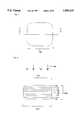
- FIG. 1is a plan view of one embodiment of the microphotodiode retinal implant of this invention (MMRI);
- FIG. 2is a cross-section taken along the plane of the line II--II of FIG. 1;
- FIG. 3is a plan view of a second embodiment of this invention (MMRI-E);
- FIG. 4is a cross-section taken along the plane of the line IV--IV of FIG. 3;
- FIG. 5shows the manufacturing process of the microphotodiode retinal implant of FIG. 1 (MMRI);
- FIG. 6is a plan view of a third embodiment of this invention (MMRI-4), which is composed of two pairs of MMRI subunits;
- FIG. 7is a perspective view in cross-section taken along the plane of line VI--VI of FIG. 6;
- FIG. 8is a plan view of a fourth embodiment of this invention (MMRI-4E), which is composed of two pairs of MMRI-E subunits;
- FIG. 9is a perspective view in cross-section taken along the plane of line VIII--VIII of FIG. 8;
- FIG. 10shows three dimensional and plan views, and a magnified inset view of a 3 inch silicon wafer secured onto a thicker 4 inch silicon wafer during the manufacture of the microphotodiode retinal implants (MMRI-4) of FIG. 6;
- FIG. 11shows the microphotodioce retinal implants (MMRI-4) of FIG. 6 implanted in the preferred location of the subretinal space;
- FIG. 12shows the microphotodiode retinal implants (MMRI-4) of FIG. 6 implanted in an alternate location, on the nerve fiber layer surface of the retina;
- FIG. 13shows a plan view of a fifth embodiment of the microphotodiode implant of this invention (MMRI-IPV);
- FIG. 14is a cross-section take along the plane of line X--X of FIG. 13.
- FIG. 15shows a plan view of a sixth embodiment of the microphotodiode implant of this invention (MMRI-IPIR);
- FIG. 16is a cross-section taken along the plane of line XII--XII of FIG. 15;
- FIG. 17shows a plan view of a seventh embodiment of the microphotodiode implant of this invention (MMRI-IPVIR-A);
- FIG. 18is a cross-section taken along the plane of line XIV--XIV of FIG. 17;
- FIG. 19shows a plan view of a eighth embodiment of the microphotodiode implant of this invention (MMRI-IPVIR-B);
- FIG. 20is a cross-section taken along the plane of line XVI--XVI of FIG. 19;
- FIG. 21is a cross-section of the retina showing the microphotodiode implants of FIG. 17 (MMRI-IPVIR-A) in their preferred location in the subretinal space, with their electrodes penetrating into the sublamina B, and sublamina A locations of the inner plexiform;
- MMRI-IPVIR-Amicrophotodiode implants of FIG. 17
- FIG. 22is a cross-section of the retina showing the microphotodiode implants of FIG. 17 with reversed polarities (MMRI-IPVIR-AR), in a ninth embodiment of this invention, in their preferred location on the nerve fiber layer surface, with their electrodes penetrating into the sublamina B, and sublamina A location of the inner plexiform;
- MMRI-IPVIR-ARreversed polarities
- FIG. 23is a generalized schematic diagram of the Adaptive Imaging Retinal Stimulation System (AIRES) showing its component sub-systems of: the Projection and Tracking Optical System (PTOS), the Neuro-Net Computer (NNC), and the Input Stylus Pad (ISP). Q-SEMCPs are shown implanted in the eye;
- PTOSProjection and Tracking Optical System
- NNCNeuro-Net Computer
- ISPInput Stylus Pad
- FIG. 24A-Dshows a PTOS device configured as a glasses headset, and the schematic of its optics
- FIG. 25shows the components of the AIRES system, consisting of the PTOS, the NNC, and ISP.
- each microphotodiode implant (106)is fabricated as a flattened cubic device (hereafter MMRI) containing a single two-side microphotodiode.
- MMRIflattened cubic device
- each MMRI (106)forms the shape of a flattened cube with rounded corners and edges, and is sized in microscopic dimensions, and is a physically independent unit.
- MMRIs (106)may function as a PiN or NiP device, depending upon which of its two photosensitive sides, the P-side (107a) or the N-side (107b) is stimulated by visible and/or infrared light (108).
- the layers of the MMRI (106)include the P electrode (110) preferably made of P doped polysilicon, a multilayer dielectric filter (122) to allow passage of only visible light (400 nm to 740 nm) to the next P+ layer (112), a contact pad (114) fabricated from any or all or compounds of the following: gold, aluminum, titanium, and chromium, to establish electrical contact between layers (110) and (112), an intrinsic layer (126) which forms naturally between the P+ layer (112) and the N-type silicon substrate (128), a N+ layer (118), a multilayer dielectric filter (124) to allow passage of only infrared light (740 nm to 900 nm) to the N+ layer (118), a contact pad (120) fabricated from any or all compounds of the following: gold, aluminum, titanium, and chromium to establish electrical contact between the N+ layer (118) and the last layer that is the N electrode (116), preferably made of N-doped polysilicon.
- FIGS. 1-2shows that the P electrode (110) and the N electrode (116) cover the entire surface of the MMRI (106), in alternate embodiments, the P electrode (110) may cover a fraction of the photosensitive side P-side (107a), and the N electrode (116) may cover a fraction of the photosensitive side N-side (107b). These fractions may range from 0.1% to 99.9%.
- the purpose of fractional coverage of the P electrode (110) and N electrode (116)is to allow concentration of electric currents produced by the MMRI (106).
- the width and depth of the MMRI (106)are the same dimensions and may vary between 5 ⁇ m and 100 ⁇ m, and the height is 25% to 50% that of the width and depth.
- MMRIs (106)may be manufactured as small as 1 ⁇ m and as large as 2000 ⁇ m in depth and width, and the width and depth need not be the same; and the height of the MMRI may be from 1% to 500% of the width and depth.
- the MMRI N-type silicon substrate (128)has an ohmic restive value between 50 and 2000 ohm-cm 2 .
- the MMRI N-type substrate (128)may have ohmic resistive values of between 1 ohm-cm 2 and 100,000 ohm-cm 2 .
- the designed and preferred electric current output of each MMRI (106)is on the order of 1 to 5000 nA depending on incident lighting (108). Nevertheless, a range of 0.01 nA to 200,000 nA is also suitable.
- MMRI-EIn a second embodiment of this invention (FIGS. 3-4), the MMRIs of FIGS. 1-2 are fabricated so that the polysilicon layer 110 is sandwiched between the multi-layer dielectric visible light filter layer 122 and the P+ layer 112, and the polysilicon layer 116 is sandwiched between the multi-layer dielectric IR filter layer 124 and the N+ layer 124.
- the aluminum contact pads 114 and 120 of FIGS. 1-2are not needed in this embodiment.
- This embodimentresults in MMRI-Es which predominately stimulate retinal cells adjacent to the MMRI-Es rather than on top of the MMRI-Es.
- This second embodimentis used in those patients where side simulation will induce better vision than top stimulation.
- the remaining layers of the intrinsic layer 126, and the N-type silicon substrate layer 128, the P-side 107a, and the N-side 107bare unchanged.
- FIG. 5A through Lillustrates the manufacturing steps of the preferred MMRIs.
- a 3" float zone 1-0-0 N-type silicon wafer (140) at 200 to 400 ohm-cmis thinned to 8 ⁇ m, and a silicon support ring (142) 0.4" to 0.5" wide (prepared by chemical etch and channel stop techniques to have 30-40 degree i.d. taper) is then oxide bonded to target wafer (140).
- P+ layer (144)is ion implanted to 0.2 ⁇ m depth on one side of the wafer (140). The other side is masked from the implantation.
- wafer (140)is flipped over and the N+ layer (146) is ion implanted to 0.2 ⁇ m depth on the second side.
- the first P+ side (144)is masked from implantation.
- both the P+ (144) and N+ (146) layersare thermally driven to 0.5 ⁇ m to 0.6 ⁇ m depth.
- 5EMultiple alternating layers of TiO 2 and quartz are evaporation deposited to produce an interference filter (148) to pass 400-740 nm visible light, but stops 740-900 nm IR light on the P+ side (144).
- the total thickness of this dielectric layer (148)is about 3.5 to 5 ⁇ m.
- the waferis flipped over to expose the N+ side (146) and multiple alternating layers of TiO 2 are evaporation deposited to produce a interference filter (150) which passes 740-900 nm IR light, but stops 400-740 nm visible light on the N+ side (146). Total thickness of this dielectric layer (150) is about 2-3 ⁇ m.
- photoresistis spun-on and both sides of the wafer (140) are patterned with 8 ⁇ m ⁇ 8 ⁇ m contact holes (152) which penetrate the interference films (148 and 150) to the P+ layer (144) and the N+ layer (146), with hole spacing of 50 ⁇ m in a square grid fashion. As shown in FIG.
- 1.0 ⁇ m of aluminum (152)is deposited to both sides of the wafer (140).
- photoresistis spun-on and both sides of the wafer (140) are patterned to leave 12 ⁇ m ⁇ 12 ⁇ m aluminum contact pads (154) over all the 8 ⁇ m ⁇ 8 ⁇ m contact holes, and then thermally drive in the aluminum.
- plasma assisted, low pressure, chemical vapor depositionis used to deposit 0.2 ⁇ m to 0.5 ⁇ m of P+ polysilicon (156) on the P+ side interference filter (148) of the wafer (140) to establish electrical contact with the aluminum contact pads (154), at 250°-300° C. The other side of wafer is masked.
- FIG. 5Iphotoresist is spun-on and both sides of the wafer (140) are patterned to leave 12 ⁇ m ⁇ 12 ⁇ m aluminum contact pads (154) over all the 8 ⁇ m ⁇ 8 ⁇ m contact holes, and then thermally drive in the aluminum.
- plasma assisted, low pressure, chemical vapor depositionis used to deposit
- FIGS. 6-7illustrate the layered microarchitecture of a third embodiment of the artificial retina device of this invention, designated at (8), and is referred to for convenience as a MMRI-4 to distinguish it from other embodiments of this invention.
- MMRI-4 (8)forms the shape of a flattened cube with rounded corners and edges, and is sized in microscopic dimensions. It is comprised of four microphotodiode subunits (10a ⁇ 2 and 10b ⁇ 2). Each microphotodiode subunit (10a or 10b) of the MMRI-4 (8) may be a PiN or NiP device, depending upon which of its photosensitive surfaces is oriented toward light (12). For example, as shown in FIG.
- the near left microphotodiode (10a)is behaving as a PiN subunit, because the P+ tub (14) is facing incident light (12).
- the near right microphotodiode (10b)is behaving as a NiP subunit because its N+ tub (18) is facing incident light (12).
- the MMRI-4 (8)is flipped over, the microphotodiode subunit (10a) will have its N+ tub (18) facing incident light and will therefore behave as a NiP device.
- the microphotodiode subunit (10b)will have a P tub (14) facing incident light and will behave as a PiN device.
- the MMRI-4 (8) in its basic formcontains four positive (P) electrodes (13) disposed on the four P+ tub (14) surfaces on the top and bottom sides of the MMRI-4 (8) (note the bottom structure of the two rear microphotodiode subunits cannot be seen in FIG. 7).
- the P electrodes (13)are preferably made of P doped polysilicon, produced by chemical vapor deposition, and are deposited on the inner corners of the P+ tubs (14).
- Interposed between the P electrodes (13) and the P+ tubs (14),is a layer of gold, titanium or chromium (14a) to promote adhesion and to act as a light block.
- the MMRI-4 (8)also contains four negative (N) electrodes (16) disposed on the four N+ tub (18) surfaces.
- the N electrodes (16)are preferably made of N-doped polysilicon, produced by chemical vapor deposition, and are deposited on the inner corners of the N+ tubs (18). Interposed between the N electrodes (16) and the N+ tubs (18) is also a layer of gold, titanium or chromium (14a) to promote adhesion and to act as a light block.
- the P electrodes (13), and N electrodes (16)may be constructed of any suitable material that will conduct electric current. These conductive materials may include, but are not limited to, gold, chromium, aluminum, iridium, and platinum or any combination or compounds made from these materials.
- the P electrodes (13) and the N electrodes (16)may cover any fraction, from 0.1% to 99.9%, of their respective P+ tub (14) or N+ tub (18) surfaces.
- Filter layers (20)are disposed on the portion of the P+ tub (14) surfaces not covered by the P electrodes (13). These filter layers (20) are preferably fabricated from multi-layer dielectric coatings and allow passage of only visible light (400 nm to 740 nm) to the P+ tub (14) surfaces.
- Filter layers (22)are disposed on the N+ tub (18) surfaces not covered by the N electrodes (16). These filter layers (22), are also preferably fabricated from multi-layer dielectric coatings and allow passage of only infrared light (740 to 900 nm) to the N+ tub (18) surfaces. Under each P+ tub (14), an intrinsic layer (15) forms naturally between the P+ tub (14) and the N-type silicon substrate (25). The N+ tub layers (18) are created by ion implantation of additional N-type phosphorus into the N-type silicon substrate (25). Ion implantation of P-type boron around each MMRI-4 subunit (10a ⁇ 2, 10b ⁇ 2) produces a channel stop (24) to electrically separate the microphotodiode subunits from each other. Outside the channel stop material (24) is surrounding N-type silicon substrate (25b).
- the width and depth of the MMRI-4 (8)are the same dimensions and are between 10 and 50 microns, and the height is 25% to 50% that of the width and depth.
- This flattened cubic configurationwill allow one or the other of the two flattened photoactive sides of the MMRI-4 (8) to be preferentially directed to incident light (12), when the MMRI-4 (8) is implanted in the subretinal space.
- MMRI-4s (8)may be manufactured as small as 1 micron and as large as 1000 microns in depth and width, and the width and depth need not be the same; further the height of the MMRI-4 may be from 1% to 500% of the width and depth. In the embodiment of FIGS.
- the MMRI-4 N type substrate (25 and 25b)has an ohmic resistive value between 50 and 2000 ohm-cm 2 .
- the MMRI-4 N-type substrate (25 and 25b)may have ohmic resistive values of between 1 ohm-cm 2 and 100,000 ohm-cm 2 .
- the designed and preferred electric current output of each MMRI-4 subunit microphotodiode (10a or 10b)is on the order of 1 to 5000 nA depending on incident lighting (12). Nevertheless, a range of 0.01 nA to 200,000 nA may also be suitable.
- the MMRI-4 (8)may also be modified to achieve greater or lesser electrical output by changing the area of each P electrode (13), and/or the N electrode (16) relative to the area of their respective P+ tub (14) and N+ tub (18).
- FIGS. 8-9illustrate the layered microarchitecture of a fourth embodiment of the artificial retina device of this invention, designated at (8a), and is referred to for convenience as a MMRI-4E to distinguish it from other embodiments of this invention.
- MMRI-4E (8a)forms the shape of a flattened cube with rounded corners and edges, and is sized in microscopic dimensions. It is comprised of four microphotodiode subunits (10a ⁇ 2 and 10b ⁇ 2). Each microphotodiode subunit (10a or 10b) of the MMRI-4E (8a) may be a PiN or NiP device, depending upon which of its photosensitive surfaces is oriented toward light (12). For example, as shown in FIG.
- the near left microphotodiode (10a)is behaving as a PiN subunit, because the P+ tub (14) is facing incident light (12).
- the near right microphotodiode (10b)is behaving as a NiP subunit because its N+ tub (18) is facing incident light (12).
- the MMRI-4E (8a)is flipped over, the microphotodiode subunit (10a) will have its N+ tub (18) facing incident light and will therefore behave as a NiP device.
- the microphotodiode subunit (10b)will have a P tub (14) facing incident light and will behave as a PiN device.
- the MMRI-4E (8a) in its basic formcontains four transparent positive (P) electrodes (13) disposed on the four P+ tub (14) surfaces on the top and bottom sides of the MMRI-4E (8a) (note the bottom structure of the two rear microphotodiode subunits cannot be seen in FIG. 9).
- the transparent P electrodes (13)are preferably made of P doped polysilicon, produced by chemical vapor deposition, and are deposited on the P+ tubs (14).
- the MMRI-4E (8a)also contains four transparent negative (N) electrodes (16) disposed on the four N+ tub (18) surfaces.
- the transparent N electrodes (16)are preferably made of N-doped polysilicon, produced by chemical vapor deposition, and are deposited on the N+ tubs (18).
- the P electrodes (13), and N electrodes (16)may be constructed of any suitable material that can be deposited in a thin transparent layer, and that will conduct electric current. These conductive materials may include, but are not limited to, gold, chromium, aluminum, iridium, and platinum or any combination or compounds made from these materials.
- Filter layers (20)are disposed on the P electrodes (13). These filter layers (20) are preferably fabricated from multi-layer dielectric coatings and allow passage of only visible light (400 nm to 740 nm) through to the transparent P electrodes (13) and then to the P+ tub (14) surfaces. Filter layers (22) are disposed on the N+ tub (18) surfaces.
- These filter layers (22),are also preferably fabricated from multi-layer dielectric coatings and allow passage of only infrared light (740 to 900 nm) through to the transparent N electrodes (16) and then to the N+ tub (18) surfaces.
- an intrinsic layer (15)forms naturally between the P+ tub (14) and the N-type silicon substrate (25).
- the N+ tub layers (18)are created by ion implantation of additional N-type phosphorus into the N-type silicon substrate (25). Ion implantation of P-type boron around each MMRI-4 subunit (10a ⁇ 2, 10b ⁇ 2) produces a channel stop (24) to electrically separate the microphotodiode subunits from each other. Outside the channel stop material (24) is surrounding N-type silicon substrate (25b).
- the width and depth of the MMRI-4E (8a)are the same dimensions and are between 10 and 50 microns, and the height is 25% to 50% that of the width and depth.
- This flattened cubic configurationwill allow one or the other of the two flattened photoactive sides of the MMRI-4E (8a) to be preferentially directed to incident light (12), when the MMRI-4E (8a) is implanted in the subretinal space.
- MMRI-4Es (8a)may be manufactured as small as 1 micron and as large as 1000 microns in depth and width, and the width and depth need not be the same; further the height of the MMRI-4E may be from 1% to 500% of the width and depth. In the embodiment of FIGS.
- the MMRI-4E N type substrate (25 and 25b)has an ohmic resistive value between 50 and 2000 ohm-cm 2 .
- the MMRI-4E N-type substrate (25 and 25b)may have ohmic resistive values of between 1 ohm-cm 2 and 100,000 ohm-cm 2 .
- the designed and preferred electric current output of each MMRI-4E subunit microphotodiode (10a or 10b)is on the order of 1 to 5000 nA depending on incident lighting (12). Nevertheless, a range of 0.01 nA to 200,000 nA may also be suitable.
- the MMRI-4E (8a)may also be modified to achieve greater or lesser electrical output by changing the thickness and therefore the transparency of each P electrode (13), and/or the N electrode (16).
- FIG. 10the manufacture of the preferred MMRI-4s (8) is illustrated.
- the first stage in the manufacture of MMRI-4sbegins with a three-inch diameter N type 1-0-0 silicon wafer (30) that is 8 microns thick. This wafer (30) is secured around its circumference to a four-inch wafer (34) approximately 500 microns thick, with titanium pins (32).
- a plurality of N-type square island groups (8) that eventually become the MMRI-4sare isolated from the surrounding N-type substrate (25b) by ion implantation of P-type boron channel stops (24) from both sides.
- the channel stops (24)are heat driven through the entire thickness of the three-inch diameter wafer (30) to isolate four square columns of N-type silicon substrate (25) per square island (8).
- Each square column (25)is 11 microns per side and separated from adjacent square columns (25) of the same MMRI-4 (8) by 1 micron of P-type silicon channel stop (24).
- the resultant square islands (8), including the channel stops (24)are 21 microns per side.
- the square islands (8)are separated from each other by 1 micron of N-type silicon substrate (25b).
- Alignment holes (36)are excimer laser drilled through the three-inch wafer (30). These holes (36) facilitate alignment of fabrication masks from either side of the three-inch wafer (30).
- the P+ tubs (14) shown in FIG. 7are created by ion implantation and thermal diffusion of P-type boron into the N-type substrate square columns (25).
- Two P+ tubs (14)are formed on each side of the MMRI-4 square island (8) and are arranged diagonally to each other.
- Intrinsic layers (15)automatically form between the P+ tubs (14) and the N type silicon substrate of the square columns (25).
- the N+ tubs (18)are created by ion implantation and thermal diffusion of additional N-type phosphorus into the N-type silicon substrate square columns (25) from the opposite side of the P+ tubs (14).
- multilayer dielectric coatings (20) that bandwidth pass visible light (400 to 740 nm), and multilayer dielectric coatings (22) that bandwidth pass infrared light (740 to 900 nm)are deposited on their respective P+ tubs (14) and the N+ tubs (18) after deposition of the gold, chromium or titanium adhesion and light block layer (14a).
- the final three-inch wafer (30), with fabricated MMRI-4 square islands (8),is then removed from the four-inch support wafer (34).
- the three-inch wafer (30)is then rebonded to the four-inch wafer (34) with an aqueous dissolvable adhesive.
- X and Y direction cutsare made to separate the MMRI-4 islands (8) from each other.
- the MMRI-4 islands (8)however, still remain bonded to the support wafer (34) by adhesive.
- the wafer assembly (30 and 34)is then placed in an aqueous solution solvent to dissolve the adhesive.
- the MMRI-4 square islands (8)are recover from the aqueous solution using standard filtering techniques, and are washed, and dried.
- the recovered MMRI-4 islands (8)are briefly tumbled in a glass container using ultrasonic energy. This tumbling process will slightly round off the sharp corners and edges of the MMRI-4s (8).
- the final devices, demonstrated by the MMRI-4s (8) of FIG. 7,are then washed again, recovered, sterilized, and then placed in a biologically compatible semi-solid or liquid vehicle for implantation into the eye.
- FIG. 11shows MMRI-4s (8) implanted in their preferred monolayer position in the subretinal space (82).
- the layers of the eye at the posterior pole from inside the eye to outside the eyeare shown in their respective positions: internal limiting membrane (50); nerve fiber layer (52); ganglion and cell layer (54); inner plexiform layer (56); inner nuclear layer (58); outer plexiform layer (60); outer nuclear cell layer (62); and photoreceptor layer (64), all of which constitute the inner retinal layer (66).
- the MMRI-4s (8)are disposed between the inner retinal layer (66), and the retinal pigment epithelium (68) and Bruch's membrane (70), which together constitute the outer retinal layer (72).
- External to the outer retinal layer (72)are the choriocapillaris (74) and choroid (76) which comprise the choroidal vasculature (78), and sclera (80), which comprised the outer coat of the eye.
- FIG. 12shows MMRI-4s (8) in an alternate embodiment location, positioned on the internal limiting membrane surface (50) of the retina and close to the nerve fiber layer (52).
- MMRI-4s (8)are embedded into a flexible, biologically compatible sheet (44), that allows both of the flattened photoactive surfaces of each MMRI-4s (8) to be exposed.
- Electrical stimulation of the retinal nerve fiber layer (52), through the internal limiting membrane surface (50) by the MMRI-4s (8)will also induce artificial vision, but the quality of images produced will not be as well formed as from stimulation of the retina from the subretinal space ((82) as shown in FIG. 11.
- choriocapillaris (74) and choroid (76)comprise the choroidal vasculature (78), and sclera (80), the outer coat of the eye.
- the two dielectric filter layers embedded in each MMRIwill be both of the visible light transmitting type (210, 222), or will be both of the IR light transmitting type (310, 322).
- the electrodes of these devicesmay be fabricated from gold, although aluminum or platinum may also be used, and will be deposited with an industry standard "wafer bumping" process. This will form each electrode into a projecting-like structure bonded to an aluminum contact pad (214, 224, 314, 324).
- Each gold projecting electrode(202, 204, 302, 304) will be then covered over its entire surface, with the exception of the tip, by an insulating layer of silicon dioxide (208, 226, 308, 326) or alternatively silicon nitrite.
- the height of the projecting electrodewill be higher on one side of the device than on the other side, and may be 5 ⁇ m to 200 ⁇ m on the higher side (202, 302) and 1 ⁇ m to 195 ⁇ m on the lower side (204, 304).
- a visible light responsive devicedesignated at (200) with a higher projecting electrode (HPE) (202) on the negative (N) side (205b), and a lower projecting electrode (LPE) (204) on the positive (P) side (205a)
- MMRI-IPVvisible light responsive device
- HPEhigher projecting electrode
- LPElower projecting electrode
- MMRI-IPIRIR light responsive device
- MMRI-IPV (200) and MMRI-IPIR (300)can also exist as a combination unit (MMRI-IPVIR-A) designated at (400), comprised of one MMRI-IPV (200) and one MMRI-IPIR (300).
- MMRI-IPVIR-Aa combination unit designated at (400), comprised of one MMRI-IPV (200) and one MMRI-IPIR (300).
- HPE (202) of the MMRI-IPV (200) and the HPE (302) MMRI-IPIR (300)will be pointed in the same direction on the one side of the MMRI-IPVIR-A.
- the LPE (204) of the MMRI-IPV (200) and the LPE (304) of the MMRI-IPIR (300)will be also pointed together in the same direction, but on the opposite side of the MMRI-IPVIR-A (400) and in a direction opposite the direction of the HPEs (202, 302).
- the MMRI-IPVIR-A (400)are disposed into the subretinal space (82) of the eye and are used to stimulate those retinas where the photoreceptor layer has completely degenerated leaving the bipolar cell layer (58a) or the inner plexiform layer (56) as the layer adjacent to the subretinal space (82).
- the HPE electrodes (202, 302)will selectively contact the "light channel” synapses in the sublamina "B” (56b) and the LPEs (204, 304) will selectively contact the "dark channel” synapses in sublamina "A" (56A).
- This arrangementwill allow a visible light stimulus to selectively depolarize and activate the light channels in sublamina "B” by causing a negative electric current to be produced by the HPE (202), and an IR light stimulus to selectively hyperpolarize and inhibit the light channels in sublamina "B” by causing a positive electric current to be produced by the HPE (302).
- This arrangementwill also allow an IR light stimulus to selectively depolarize and activate the dark channels in sublamina "A” by causing a negative electric current to be produced by the LPE (304), and a visible light stimulus to selectively hyperpolarize and inhibit the dark channels in sublamina "A” by causing a positive electric current to be produced by the LPE (204).
- MMRI-4 (8), and reversed polarity MMRI-IPVIR-A implants called for convenience, MMRI-IPVIR-ARs (8c),are embedded into a biologically compatible sheet (44) that allows the electrode surfaces of the devices to be exposed.
- the sheet (44), with the embedded MMRI-4 (8)is placed on the internal limiting membrane surface (50) of the retina from the vitreous body side. From this location, MMRI-4s (8) will stimulate the Nerve Fiber Layer (52) and/or Ganglion Cells (54) of the retina.
- polarization changesi.e. hyperpolarization and depolarization, do not have the same effect in the subretinal space on remanent photoreceptor cells as they do in the sublamina B and A regions of the IPL.
- a hyperpolarizing stimulusproduces a sensation of light in the remanent photoreceptor cells while a depolarizing stimulus produces a sensation of darkness in remanent photoreceptor cells.
- FIGS. 13-14therefore illustrate a fifth embodiment of this invention referred to for convenience as a "MMRI-IPV", and is sized in microscopic dimensions, and is designated at (200).
- MMRI-IPV (200)is a physically independent unit with its layered microarchitecture shown in FIG. 14.
- the MMRI-IPV (200)forms the shape of a flattened cube with rounded corners and edges, with an electrically negative high projecting electrode (“HPE”) (202), and an electrically positive low projecting electrode (“LPE”) (204).
- HPEhigh projecting electrode
- LPEelectrically positive low projecting electrode
- a MMRI-IPV (200)may function as a PiN or NiP device when stimulating the inner retina, depending upon which of its two photosensitive sides, the P side (205a) or the N side (205b) is stimulated by visible light (206).
- the layers of the MMRI-IPV (200)are as follows: A negative HPE electrode (202) preferably made of gold, an insulating layer of SiO 2 (208) which covers the N side (205b) except for the tip of the HPE electrode (202), a multilayer dielectric filter (210) to allow passage of only visible light (400 nm to 740 nm), a N+ layer (212), a contact pad (214) fabricated from any of the following, and/or any compounds of the following: gold, aluminum, titanium, and chromium, to establish electrical contact between the negative HPE (202) and the N+ layer (212), a N-type silicon substrate layer (216), an intrinsic layer (218) which forms naturally between the N-type silicon substrate layer (216), and the next P+ layer (2
- FIGS. 15-16illustrates a sixth embodiment of this invention referred to for convenience as a "MMRI-IPIR", and is sized in microscopic dimensions, and is designated at (300).
- a MMRI-IPIR (300)is a physically independent unit with its layered microarchitecture is shown in FIG. 16.
- the MMRI-IPIR (300)forms the shape of a flattened cube with rounded corners and edges, with an electrically positive high projecting electrode (HPE) (302), and an electrically negative low projecting electrode (LPE) (304).
- HPEhigh projecting electrode
- LPEelectrically negative low projecting electrode
- a MMRI-IPIR (300)may function as a PiN or NiP device when stimulating the inner retina, depending upon which of its two photosensitive sides, the N-side (305a) or the P-side (305b) is stimulated by infrared light (306).
- the layers of the MMRI-IPIR(300)are as follows: A positive HPE electrode (302) preferably made of gold, an insulating layer of SiO 2 (308) which covers the P side (305b) except for the tip of the positive HPE electrode (302), a multilayer dielectric filter (310) to allow passage of only IR light (740 nm to 900 nm), a P+ layer (312), a contact pad (314) fabricated from any of the following and/or any compounds of the following: gold, aluminum, titanium, and chromium, to establish electrical contact between the positive HPE (302) and the P+ layer (312), an intrinsic layer (318) which forms naturally between the P+ layer (312) and the next N-type silicon substrate layer (316), a N+ layer (320), a multilayer dielectric filter (322) to allow passage of only IR light (740 nm to 900 nm), a contact pad (324) fabricated from any of the following and/or any compounds of the following: gold, aluminum, titanium, and
- FIGS. 17-18illustrate a seventh embodiment of this invention referred to for convenience as a "MMRI-IPVIR-A", and is sized in microscopic dimensions, and is designated at 400. It is composed of one MMRI-IPV (200), and one MMRI-IPIR (300), separate by a layer of channel block (350).
- the layered microarchitecture of the MMRI-IPV component (200)is shown on the left side and is described first.
- the MMRI-IPV component (200)forms the shape of one-half of a flattened cube with rounded external corners and edges, with an electrically negative high projecting electrode (HPE) (202), and an electrically positive low projecting electrode (LPE) (204).
- HPEelectrically negative high projecting electrode
- LPEelectrically positive low projecting electrode
- the layers of the MMRI-IPV (200)are as follows: A negative HPE electrode (202) preferably made of gold, an insulating layer of SiO 2 (208) which covers the N side (205b) except for the tip of the HPE electrode (202), a multilayer dielectric filter (210) to allow passage of only visible light (400 nm to 740 nm), a N+ layer (212), a contact pad (214) fabricated from any of the following and/or any compounds of the following: gold, aluminum, titanium, and chromium, to establish electrical contact between the negative HPE (202) and the N+ layer (212), a N-type silicon substrate layer (216), an intrinsic layer (218) which forms naturally between the N-type silicon substrate layer (216), and the next P+ layer (220), a multilayer dielectric filter (222) to allow passage of only visible light (400 nm to 740 nm), a contact pad (224) fabricated from any of the following and/or any compounds of the following: gold, aluminum, titanium, and
- An insulating layer of SiO 2 (226)covers the P side (205a) except for the tip of the LPE electrode (204).
- the layered microarchitecture of the MMRI-IPIR component (300) of the MMRI-IPVIR-A (400)is shown on the right side and is now described.
- the MMRI-IPIR component (300)forms the shape of one-half of a flattened cube with rounded external corners and edges, with an electrically positive high projecting electrode (HPE) (302), and an electrically negative low projecting electrode (LPE) (304).
- HPEhigh projecting electrode
- LPEelectrically negative low projecting electrode
- the layers of the MMRI-IPIR (300)are as follows: A positive HPE electrode (302) preferably made of gold, an insulating layer of SiO 2 (308) which covers the P side (305b) except for the tip of the positive HPE electrode (302), a multilayer dielectric filter (310) to allow passage of only IR light (740 nm to 900 nm), a P+ layer (312), a contact pad (314) fabricated from any of the following and/or any compounds of the following: gold, aluminum, titanium, and chromium, to establish electrical contact between the positive HPE (302) and the P+ layer (312), an intrinsic layer (318) which forms naturally between the P+ layer (312) and the next N-type silicon substrate layer (316), a N+ layer (320), a multilayer dielectric filter (322) to allow passage of only IR light (740 nm to 900 nm), a contact pad (324) fabricated from any of the following and/or any compounds of the following: gold, aluminum, titanium, and
- FIGS. 19-20illustrate an eighth embodiment of this invention referred to for convenience as a "MMRI-IPVIR-B", and is sized in microscopic dimensions, and is designated at 500. It is composed of one MMRI-IPV (200), and one MMRI-IPIR(300), separate by a layer of channel block (350).
- the layered microarchitecture of the MMRI-IPV component (200)is shown on the left side and is described first.
- the MMRI-IPV component (200)forms the shape of one-half of a flattened cube with rounded external corners and edges, with an electrically negative high projecting electrode (HPE) (202), and an electrically positive low projecting electrode (LPE) (204).
- HPEelectrically negative high projecting electrode
- LPEelectrically positive low projecting electrode
- the layers of the MMRI-IPV (200)are as follows: A negative HPE electrode (202) preferably made of gold, an insulating layer of SiO 2 (208) which covers the N side (205b) except for the tip of the negative HPE electrode (202), a multilayer dielectric filter (210) to allow passage of only visible light (400 nm to 740 nm), a N+ layer (212), a contact pad (214) fabricated from any of the following and/or any compounds of the following: gold, aluminum, titanium, and chromium, to establish electrical contact between the negative HPE (202) and the N+ layer (212), a N-type silicon substrate layer (216), an intrinsic layer (218) which forms naturally between the N-type silicon substrate layer (216), and the next P+ layer (220), a multilayer dielectric filter (222) to allow passage of only visible light (400 nm to 740 nm), a contact pad (224) fabricated from any of the following and/or any compounds of the following: gold, aluminum, titanium,
- An insulating layer of SiO 2 (226)covers the P side (205a) except for the tip of the LPE electrode (204).
- the layered microarchitecture of the MMRI-IPIR component (300) of the MMRI-IPVIR-B (500)is shown on the right side and is now described.
- the MMRI-IPIR component (300)forms the shape of one-half of a flattened cube with rounded external corners and edges, with an electrically positive high projecting electrode (HPE) (302), and an electrically negative low projecting electrode (LPE) (304).
- the layers of the MMRI-IPIR (300)are as follows: A positive HPE electrode (302) preferably made of gold, an insulating layer of SiO 2 (308) which covers the P side (305b) except for the tip of the positive HPE electrode (302), a multilayer dielectric filter (310) to allow passage of only IR light (740 nm to 900 nm), a P+ layer (312), a contact pad (314) fabricated from any of the following and/or any compounds of the following: gold, aluminum, titanium, and chromium, to establish electrical contact between the positive HPE (302) and the P+ layer (312), an intrinsic layer (318) which forms naturally between the P+ layer (312) and the next N-type silicon substrate layer (316), a N+ layer (320), a multilayer dielectric filter (322) to allow passage of only IR light (740 nm to 900 nm), a contact pad (324) fabricated from any of the following and/or any compounds of the following: gold, aluminum, titanium, and
- FIG. 21shows MMRI-IPVIR-As (400) implanted in their preferred monolayer position in the subretinal space (82).
- the depolarizing high projecting electrodes (HPEs) (202) from the visible light sensing portion of the microphotodiodesstimulate the light channels in sublamina B (56b) of the inner plexiform layer (IPL) (56).
- the hyperpolarizing HPEs (302) from the IR light sensing portion of the microphotodiodes (for darkness detection)inhibit the light channels in sublamina B (56b) of the IPL (56).
- the depolarizing low projecting electrodes (LPEs) (304) from the IR light sensing portion of the microphotodiodes (for darkness detection)stimulate the dark channels in sublamina A (56a) of the IPL (56).
- the hyperpolaring LPEs (204) from the visible light sensing portion of the microphotodiodeinhibit the dark channels in sublamina A (56a) of the IPL (56).
- the layers of the eye, in this schematic of a partially degenerated retina, at the posterior pole from inside the eye to outside the eyeare: internal limiting membrane (50); nerve fiber layer (52); ganglion cell layer (54); inner plexiform layer (56) consisting of sublamina b (56b) and sublamina a (56a); and the partially degenerated inner nuclear layer (58a).
- the MMRI-IPVIR-A (400)are disposed between the partially degenerated inner retinal layer (66a), and the retinal pigment epithelium (68) and Bruch's membrane (70), which together constitute the outer retinal layer (72).
- External to the outer retinal layer (72)are the choriocapillaris (74), choroid (76), and sclera (80).
- MMRI-IPVIR-As (400)instead of MMRI-IPVIR-As (400), component MMRI-IPVs and MMRI-IPIRs of FIGS. 13-16, or MMRI-IPVIR-Bs of FIGS. 19-20 can be implanted into the subretinal space (82).
- FIG. 22shows MMRI-IPVIR-ARs (8c) in a ninth embodiment of this invention, positioned on the internal limiting membrane surface (50) of the retina.
- MMRI-IPVIR-ARs (8c)are embedded into a flexible, biologically compatible sheet (44), which allows both of the photoactive surfaces and their projecting electrodes of each MMRI-IPVIR-ARs (8c) to be exposed.
- the depolarizing high projecting electrodes (HPEs) (302a) on the opposite side of the IR sensing microphotodiodes (for darkness detection)penetrate into the dark channels in sublamina A (56a) of the inner plexiform layer (IPL) (56) to stimulate the sensation of darkness.
- HPEsdepolarizing high projecting electrodes
- the layers of the eye at the posterior pole from inside the eye to outside the eye in this schematic of a partially degenerated retinaare: internal limiting membrane (50); nerve fiber layer (52); ganglion cell layer (54); inner plexiform layer (56) consisting of sublamina b (56b) and sublamina a (56a); the partially degenerated inner nuclear layer (58a); all of which constitute the partially degenerated inner retinal layer (66a).
- External to the outer retinal layer (72)are the choriocapillaris (74), choroid (76), and sclera (80).
- MMRI-IPVIR-ARs (8c)may be fabricated as component opposite polarity MMRI-IPVs and component opposite polarity MMRI-IPIRs, embedded into a flexible, biologically compatible sheet (44), which allows both of the photoactive surfaces and their projecting electrodes of each opposite polarity MMRI-IPV and opposite polarity MMRI-IPIR to be exposed.
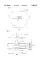
- FIG. 23is a schematic diagram of the Adaptive Imaging Retinal Stimulation System (AIRES) showing its component sub-systems of: the Projection and Tracking Optical System (PTOS) headset (94), the Neuro-Net Computer (NNC) (96), the Imaging CCD Camera (IMCCD) (100) and the Input Stylus Pad (ISP) (102).
- PTOSProjection and Tracking Optical System
- NNCNeuro-Net Computer
- ICCDImaging CCD Camera
- ISPInput Stylus Pad
- a Pupil Reflex Tracking CCD (PRTCCD) (98), and an IR/visible CRT display (IRVCRT) (92)is inside the PTOS (94).
- MMRI-4s (8)are shown in the subretinal space of the eye (90). During function, IR and visible light images from the IRVCRT (92) within the PTOS (94) are optically projected onto the eye (90).
- Intensity, wavelength duration, and pulsing of the imagesis controlled by the NNC (96) and modulated by patient inputs via the interfaced ISP (102).
- the IMCCD (100)which is mounted on or in the PTOS headset (94), provides the image inputs to the NNC (96) which in turn programs the visible and IR image outputs of the IRVCRT (92).
- a PRTCCD (98)is integrated into the PTOS headset (94) to track eye movements via changes in the position of the pupillary Purkinje reflexes.
- the PRTCCD (98)will output to the NNC (96) which in turn will direct the aim of the IMCCD (100) via servo motor control to follow the eye movements.
- the PTOS (94)also may be programmed to provide just a diffuse IR illumination to interact with ambient visible light images (104) on the MMRI-4s (8).
- a patient with a large plurality of implanted MMRI-4s (8)will see pixelated images, cause by localized subretinal hyperpolarization, produced by the PiN configuration of the MMRI-4 subunits (10a). These electrically induced images are caused by the light from incoming ambient images (104) which pass through an external partially reflective and transmissive mirror (106) of the PTOS (94). Images of dark details are induced by depolarizing currents produced by the NiP configuration of MMRI-4 subunits (10b), which are stimulated by IR illumination and/or images provided by the IRVCRT (92).
- the IRVCRT (92)is programmed by the NNC (96) to provide diffuse IR illumination and/or IR images to superimpose upon the visible light images (104) from incoming light.
- Image information for the NNC (96)is obtained from the interfaced IMCCD (100).
- Diffuse IR illumination from the IRVCRT (92)will induce a constant depolarizing "bias current" from the MMRI-4 Nip subunits (10b). This "bias current" will produce the sensation of darkness in the absence of light stimulation to the PiN subunits (10a). However, when light is present to stimulate the PiN subunits (10a), the resultant hyperpolarizing current will offset the IR induced NiP depolarizing bias current. The result is the perception by the patient of a sensation of light.
- NiP depolarizing bias currentwill be initially adjusted by the patient via the ISP (102) and this information will be inputted into the NNC (96). It is then correlated with image processed information coming from the interfaced IMCCD (100). The appropriate amount of NiP "bias current", base upon environmental lighting conditions and images, will then be "learned” by the NNC (96). With additional learning, the NNC (96) will be able to anticipate the amount of NiP "bias current” needed to produce more accurate patient perceived images, without the need for patient input.
- the entire visible light imagemay also be projected by the IRVCRT (92) simultaneously, or in rapid alternation with IR image pulses to entirely control MMRI-4(B) function.
- the partially reflective/transmissive mirror (106) of the PTOS (94)is replaced with a completely reflective mirror, to prevent ambient light images (104) from stimulating the MMRI-4s (8).
- color visionmay possibly be induced, similar to the effect of the Benham top. This phenomenon has also been used in black and white television displays to create the perception of color images in normal sighted persons.
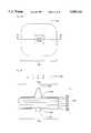
- FIGS. 24, A through Dshows a glasses-like configuration (94) of the PTOS component of the AIRES system.
- FIG. 24Dshows the schematic of the optical system differs somewhat from the generalize schematic of the PTOS component (94) demonstrated in FIG. 23, the spirit and function of both versions of the devices are the same.
- FIG. 24Ais a top view of the PTOS (94). It shows the headpad (108), the temple pieces (110), and the ambient light intensity sensors (112).
- FIG. 24Bis a front view of the PTOS (94). It shows the external partially reflective/transmissive mirror (106), a supporting nose piece (114), ambient light intensity sensors (112), and the window for the IMCCD (100) shown in the FIG. 23 schematic.
- FIG. 24Ais a top view of the PTOS (94). It shows the headpad (108), the temple pieces (110), and the ambient light intensity sensors (112).
- FIG. 24Bis a front view of the PTOS (94). It shows the external partially reflective/trans
- FIG. 24Cis a phantom side view of the PTOS (94). It shows an internal infrared and visible light capable LED light source (92), which has been substituted for the IRVCRT (92) of FIG. 23. Also shown is the partially reflective/transmissive mirror (106), the supporting nose piece (114), the headpad (108), one of the temple pieces (110), and the power supply and signal wire cable (116) to the NNC (96) of FIG. 23.
- FIG. 24Dis a schematic of the PTOS (94). It shows the MMRI-4s (8) disposed in the subretinal space of the eye (90) with an ambient focused image (104). It also shows the internal infrared and visible light capable LED light source (92), the PRTCCD (98), and the external partially reflective/transmissive mirror (106).
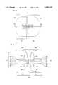
- FIG. 25is diagram showing the components of the AIRES system, consisting of the PTOS (94), the portable NNC (96) which may be secured to the patient's body, and the ISP (102) input device.
Landscapes
- Health & Medical Sciences (AREA)
- Life Sciences & Earth Sciences (AREA)
- Biomedical Technology (AREA)
- Engineering & Computer Science (AREA)
- Animal Behavior & Ethology (AREA)
- General Health & Medical Sciences (AREA)
- Public Health (AREA)
- Veterinary Medicine (AREA)
- Nuclear Medicine, Radiotherapy & Molecular Imaging (AREA)
- Heart & Thoracic Surgery (AREA)
- Ophthalmology & Optometry (AREA)
- Radiology & Medical Imaging (AREA)
- Vascular Medicine (AREA)
- Cardiology (AREA)
- Prostheses (AREA)
Abstract
Description
Claims (46)
Priority Applications (19)
| Application Number | Priority Date | Filing Date | Title |
|---|---|---|---|
| US08/465,766US5895415A (en) | 1995-06-06 | 1995-06-06 | Multi-phasic microphotodiode retinal implant and adaptive imaging retinal stimulation system |
| ES96918042TES2218589T3 (en) | 1995-06-06 | 1996-06-04 | RETINAL IMPLANT OF MULTIPHASIC MICROPHOTODYODE. |
| AU60399/96AAU709207B2 (en) | 1995-06-06 | 1996-06-04 | Multi-phasic microphotodiode retinal implant and adaptive imaging retinal stimulation system |
| AT04008614TATE326260T1 (en) | 1995-06-06 | 1996-06-04 | ARRANGEMENT FOR IRRITATING THE RETINA USING ADAPTIVE IMAGE GENERATION |
| KR1019970708632AKR100485054B1 (en) | 1995-06-06 | 1996-06-04 | Multi-phasic microphotodiode retinala implant and adaptive imaging retinal stimulation system |
| DK96918042TDK0957975T3 (en) | 1995-06-06 | 1996-06-04 | Retinal implant with multi-phase microphoto diodes |
| EP04008614AEP1435255B1 (en) | 1995-06-06 | 1996-06-04 | Adaptive imaging retinal stimulation system |
| DE69636151TDE69636151T2 (en) | 1995-06-06 | 1996-06-04 | Arrangement for irritation of the retina by means of adaptive imaging |
| CA002222741ACA2222741C (en) | 1995-06-06 | 1996-06-04 | Multi-phasic microphotodiode retinal implant and adaptive imaging retinal stimulation system |
| AT96918042TATE264702T1 (en) | 1995-06-06 | 1996-06-04 | RETINAL IMPLANT MADE OF MULTIPHASE MICROPHOTODIODES |
| KR10-2004-7004235AKR100485053B1 (en) | 1995-06-06 | 1996-06-04 | Multi-phasic microphotodiode retinal implant and adaptive imaging stimulation system |
| DE69632272TDE69632272T2 (en) | 1995-06-06 | 1996-06-04 | RETINAL IMPLANT FROM MULTIPHASE MICROPOTODIODS |
| PCT/US1996/008734WO1996039221A1 (en) | 1995-06-06 | 1996-06-04 | Multi-phasic microphotodiode retinal implant and adaptive imaging retinal stimulation system |
| NZ310074ANZ310074A (en) | 1995-06-06 | 1996-06-04 | Dual pin nip microphotodiode retinal implants |
| JP50123597AJP3514464B2 (en) | 1995-06-06 | 1996-06-04 | Multiphase microphotodiode retinal implant and corresponding imaging retinal stimulation system |
| EP96918042AEP0957975B9 (en) | 1995-06-06 | 1996-06-04 | Multi-phasic microphotodiode retinal implant |
| US09/100,336US6230057B1 (en) | 1995-06-06 | 1998-03-26 | Multi-phasic microphotodiode retinal implant and adaptive imaging retinal stimulation system |
| US09/824,519US6611716B2 (en) | 1995-06-06 | 2001-04-02 | Multi-phasic microphotodiode retinal implant and adaptive imaging retinal stimulation system |
| US10/600,404US7139612B2 (en) | 1995-06-06 | 2003-06-20 | Multi-phasic microphotodiode retinal implant and adaptive imaging retinal stimulation system |
Applications Claiming Priority (1)
| Application Number | Priority Date | Filing Date | Title |
|---|---|---|---|
| US08/465,766US5895415A (en) | 1995-06-06 | 1995-06-06 | Multi-phasic microphotodiode retinal implant and adaptive imaging retinal stimulation system |
Related Child Applications (1)
| Application Number | Title | Priority Date | Filing Date |
|---|---|---|---|
| US64270296AContinuation-In-Part | 1995-06-06 | 1996-06-03 |
Publications (1)
| Publication Number | Publication Date |
|---|---|
| US5895415Atrue US5895415A (en) | 1999-04-20 |
Family
ID=23849075
Family Applications (1)
| Application Number | Title | Priority Date | Filing Date |
|---|---|---|---|
| US08/465,766Expired - LifetimeUS5895415A (en) | 1995-06-06 | 1995-06-06 | Multi-phasic microphotodiode retinal implant and adaptive imaging retinal stimulation system |
Country Status (1)
| Country | Link |
|---|---|
| US (1) | US5895415A (en) |
Cited By (170)
| Publication number | Priority date | Publication date | Assignee | Title |
|---|---|---|---|---|
| US6032062A (en)* | 1995-08-10 | 2000-02-29 | Nmi Naturwissenschaftliches Und Medizinisches Institut | Microelectrode arrangement |
| US6120461A (en)* | 1999-08-09 | 2000-09-19 | The United States Of America As Represented By The Secretary Of The Army | Apparatus for tracking the human eye with a retinal scanning display, and method thereof |
| WO2000056393A1 (en)* | 1999-03-24 | 2000-09-28 | Second Sight, Llc | Retinal color prosthesis for color sight restoration |
| US6230057B1 (en) | 1995-06-06 | 2001-05-08 | Optobionics Corporation | Multi-phasic microphotodiode retinal implant and adaptive imaging retinal stimulation system |
| US6298270B1 (en)* | 1996-10-23 | 2001-10-02 | Eberhard-Karls-Universitat Tubingen Universitatsklinkum | Retina implant |
| US6310987B1 (en)* | 1997-06-10 | 2001-10-30 | Mitsubishi Denki Kabushiki Kaisha | Image processor |
| WO2001083026A1 (en) | 2000-05-04 | 2001-11-08 | Optobionics Corporation | Artificial retina device with stimulating and ground return electrodes disposed on opposite sides of the neuroretina and method of attachment |
| US6324429B1 (en)* | 1998-05-08 | 2001-11-27 | Massachusetts Eye And Ear Infirmary | Chronically implantable retinal prosthesis |
| US6347250B1 (en)* | 1996-10-23 | 2002-02-12 | Nmi Univ Tuebingen | Optically controllable microelectrode array for stimulating cells within a tissue |
| US6389317B1 (en) | 2000-03-31 | 2002-05-14 | Optobionics Corporation | Multi-phasic microphotodetector retinal implant with variable voltage and current capability |
| US6458157B1 (en)* | 1997-08-04 | 2002-10-01 | Suaning Gregg Joergen | Retinal stimulator |
| US6507758B1 (en) | 1999-03-24 | 2003-01-14 | Second Sight, Llc | Logarithmic light intensifier for use with photoreceptor-based implanted retinal prosthetics and those prosthetics |
| US6533798B2 (en) | 1999-01-05 | 2003-03-18 | Second Sight, Llc | Intraocular electrode |
| US20030158588A1 (en)* | 2002-01-17 | 2003-08-21 | Rizzo Joseph F. | Minimally invasive retinal prosthesis |
| US20030187491A1 (en)* | 2002-03-28 | 2003-10-02 | Robert Greenberg | Variable pitch electrode array |
| WO2004011080A1 (en)* | 2002-07-30 | 2004-02-05 | Second Sight, Llc | Field focusing and mapping in an electrode array |
| US20040030383A1 (en)* | 2002-06-06 | 2004-02-12 | Havey Gary David | Method and apparatus for sensory substitution, vision prosthesis, or low-vision enhancement utilizing thermal sensing |
| US20040039401A1 (en)* | 2000-03-31 | 2004-02-26 | Chow Alan Y. | Implant instrument |
| US20040102843A1 (en)* | 2001-03-30 | 2004-05-27 | Toru Yagi | Artificial eye system |
| US20040116980A1 (en)* | 2001-02-15 | 2004-06-17 | Jun Ohta | Vision regeneration assisting apparatus |
| WO2004067088A1 (en)* | 2003-01-31 | 2004-08-12 | Eberhard-Karls-Univer Sität Tübingen | Retina implant for stimulating a retina according to incident light |
| WO2004087024A1 (en)* | 2003-04-04 | 2004-10-14 | Carl Zeiss | Energy supply device for a retina implant |
| US20040236389A1 (en)* | 2003-05-01 | 2004-11-25 | Wolfgang Fink | Method and system for training a visual prosthesis |
| US20050004625A1 (en)* | 2001-06-29 | 2005-01-06 | Chow Alan Y. | Treatment of degenerative retinal disease via electrical stimulation of surface structures |
| WO2005000395A1 (en)* | 2003-06-23 | 2005-01-06 | Eberhard-Karls-Universität Tübingen Universitätsklinikum | Active retina implant comprising a plurality of picture elements |
| US20050010266A1 (en)* | 2003-03-24 | 2005-01-13 | Les Bogdanowicz | Device and methodology for ocular stimulation |
| US20050015120A1 (en)* | 2003-07-11 | 2005-01-20 | Seibel Eric J. | Scanning laser device and methods of use |
| US20050033202A1 (en)* | 2001-06-29 | 2005-02-10 | Chow Alan Y. | Mechanically activated objects for treatment of degenerative retinal disease |
| US20050090875A1 (en)* | 2003-09-10 | 2005-04-28 | Palanker Daniel V. | Optical projection and tracking system for retinal prosthesis |
| US20060074461A1 (en)* | 2004-07-23 | 2006-04-06 | Nidek Co., Ltd. | Visual restoration aiding device |
| US7031776B2 (en) | 2001-06-29 | 2006-04-18 | Optobionics | Methods for improving damaged retinal cell function |
| US20060085030A1 (en)* | 2004-10-15 | 2006-04-20 | Bettuchi Michael J | Seal element for anastomosis |
| US20060085034A1 (en)* | 2004-10-18 | 2006-04-20 | Bettuchi Michael J | Support structures and methods of using the same |
| US7037943B2 (en) | 2001-04-10 | 2006-05-02 | Optobionics Corporation | Retinal treatment method |
| US20060116740A1 (en)* | 2002-01-23 | 2006-06-01 | Nidek Co., Ltd. | Ophthalmic treatment apparatus |
| US20060135992A1 (en)* | 2004-10-18 | 2006-06-22 | Bettuchi Michael J | Annular adhesive structure |
| US20060148254A1 (en)* | 2005-01-05 | 2006-07-06 | Mclean George Y | Activated iridium oxide electrodes and methods for their fabrication |
| RU2282420C2 (en)* | 2004-08-09 | 2006-08-27 | Общество с ограниченной ответственностью "ИМПЛАНТ" | Epiretinal implant |
| US20070203510A1 (en)* | 2006-02-28 | 2007-08-30 | Bettuchi Michael J | Annular disk for reduction of anastomotic tension and methods of using the same |
| US20080046033A1 (en)* | 2006-07-28 | 2008-02-21 | Mcclure Kelly H | Visual Prosthesis |
| US20080066500A1 (en)* | 2006-09-15 | 2008-03-20 | Shun-Chang Su | Cable lock that is opened forcibly |
| US20080110959A1 (en)* | 2002-06-17 | 2008-05-15 | Tyco Healthcare Group Lp | Annular support structures |
| US20080140115A1 (en)* | 2004-08-17 | 2008-06-12 | Stopek Joshua B | Stapling Support Structures |
| WO2007142960A3 (en)* | 2006-05-31 | 2008-08-28 | Univ Indiana Res & Tech Corp | Laser scanning digital camera with simplified optics and potential for multiply scattered light imaging |
| US20080228242A1 (en)* | 2003-05-01 | 2008-09-18 | California Institute Of Technology | Method and system for training a visual prosthesis |
| US20080288067A1 (en)* | 2007-05-10 | 2008-11-20 | Newcyte, Inc. | Artificial retinal implant |
| US20080308608A1 (en)* | 2007-06-18 | 2008-12-18 | Prommersberger Megan L | Interlocking buttress material retention system |
| US20080314960A1 (en)* | 2007-06-22 | 2008-12-25 | Stanislaw Marczyk | Detachable buttress material retention systems for use with a surgical stapling device |
| US20090001122A1 (en)* | 2007-06-27 | 2009-01-01 | Megan Prommersberger | Buttress and surgical stapling apparatus |
| US20090095792A1 (en)* | 2006-02-28 | 2009-04-16 | Bettuchi Michael J | Hub for positioning annular structure on a surgical device |
| US20090134200A1 (en)* | 2007-03-06 | 2009-05-28 | Danyel Tarinelli | Surgical stapling apparatus |
| US20090216295A1 (en)* | 2006-04-28 | 2009-08-27 | Eberhart Zrenner | Active sub-retina implant |
| US20090222063A1 (en)* | 2006-09-26 | 2009-09-03 | Albrecht Rothermel | Implantable device |
| US20090222062A1 (en)* | 2006-09-26 | 2009-09-03 | Albrecht Rothermel | Implantable device |
| US20090218384A1 (en)* | 2007-06-18 | 2009-09-03 | Ernie Aranyi | Structure for attachment of buttress material to anvils and cartridges of surgical staplers |
| US20090287230A1 (en)* | 2005-03-15 | 2009-11-19 | Tyco Healthcare Group Lp | Anastomosis composite gasket |
| US20100012704A1 (en)* | 2007-03-06 | 2010-01-21 | Danyel Tarinelli Racenet | Surgical Stapling Apparatus |
| US20100065606A1 (en)* | 2006-10-26 | 2010-03-18 | Stopek Megan L | Methods of Using Shape Memory Alloys for Buttress Attachment |
| US20100128221A1 (en)* | 2006-05-31 | 2010-05-27 | Indiana University Research And Technology Corporation | Laser scanning digital camera with pupil periphery illumination and potential for multiply scattered light imaging |
| US20100147923A1 (en)* | 2005-03-15 | 2010-06-17 | Tyco Healthcare Group Lp | Circular anastomosis structures |
| US20100147922A1 (en)* | 2008-12-16 | 2010-06-17 | Tyco Healthcare Group Lp | Surgical Apparatus Including Surgical Buttress |
| US20100204754A1 (en)* | 2009-02-09 | 2010-08-12 | Rainbow Medical Ltd. | Retinal prosthesis |
| US20100241060A1 (en)* | 2009-03-18 | 2010-09-23 | Roizman Keith | Surgical devices and methods |
| US20100243708A1 (en)* | 2009-03-31 | 2010-09-30 | Ernie Aranyi | Surgical stapling apparatus |
| US20100243707A1 (en)* | 2009-03-31 | 2010-09-30 | Lee Olson | Surgical stapling apparatus |
| US20100249877A1 (en)* | 2007-11-21 | 2010-09-30 | The Trustees Of Boston College | Apparatus and Methods for Visual Perception Using an Array of Nanoscale Waveguides |
| US20110042442A1 (en)* | 2004-10-18 | 2011-02-24 | Tyco Healthcare Group Lp | Annular Adhesive Structure |
| US20110101070A1 (en)* | 2007-05-25 | 2011-05-05 | Tyco Healthcare Group Lp | Staple buttress retention system |
| US7967179B2 (en) | 2009-03-31 | 2011-06-28 | Tyco Healthcare Group Lp | Center cinch and release of buttress material |
| US20110172736A1 (en)* | 2010-01-14 | 2011-07-14 | Nano-Retina, Inc. | Penetrating electrodes for retinal stimulation |
| US8180453B2 (en) | 1999-03-24 | 2012-05-15 | Second Sight Medical Products, Inc. | Electrode array for neural stimulation |
| US8348130B2 (en) | 2010-12-10 | 2013-01-08 | Covidien Lp | Surgical apparatus including surgical buttress |
| US8428740B2 (en) | 2010-08-06 | 2013-04-23 | Nano-Retina, Inc. | Retinal prosthesis techniques |
| US8442641B2 (en) | 2010-08-06 | 2013-05-14 | Nano-Retina, Inc. | Retinal prosthesis techniques |
| US8479968B2 (en) | 2011-03-10 | 2013-07-09 | Covidien Lp | Surgical instrument buttress attachment |
| US8561873B2 (en) | 2009-10-15 | 2013-10-22 | Covidien Lp | Staple line reinforcement for anvil and cartridge |
| US8571669B2 (en) | 2011-02-24 | 2013-10-29 | Nano-Retina, Inc. | Retinal prosthesis with efficient processing circuits |
| US8584920B2 (en) | 2011-11-04 | 2013-11-19 | Covidien Lp | Surgical stapling apparatus including releasable buttress |
| US8631989B2 (en) | 2009-03-31 | 2014-01-21 | Covidien Lp | Surgical stapling apparatus |
| US8706243B2 (en) | 2009-02-09 | 2014-04-22 | Rainbow Medical Ltd. | Retinal prosthesis techniques |
| US8820606B2 (en) | 2012-02-24 | 2014-09-02 | Covidien Lp | Buttress retention system for linear endostaplers |
| US8967448B2 (en) | 2011-12-14 | 2015-03-03 | Covidien Lp | Surgical stapling apparatus including buttress attachment via tabs |
| US20150065837A1 (en)* | 1996-09-04 | 2015-03-05 | Geelux Holding, Ltd. | Device for generating a detectable signal based upon concentration of at least one substance |
| US9010609B2 (en) | 2012-01-26 | 2015-04-21 | Covidien Lp | Circular stapler including buttress |
| US9010608B2 (en) | 2011-12-14 | 2015-04-21 | Covidien Lp | Releasable buttress retention on a surgical stapler |
| US9010612B2 (en) | 2012-01-26 | 2015-04-21 | Covidien Lp | Buttress support design for EEA anvil |
| US9084602B2 (en) | 2011-01-26 | 2015-07-21 | Covidien Lp | Buttress film with hemostatic action for surgical stapling apparatus |
| US9113885B2 (en) | 2011-12-14 | 2015-08-25 | Covidien Lp | Buttress assembly for use with surgical stapling device |
| US20150246220A1 (en)* | 2012-05-09 | 2015-09-03 | Po-Kang Lin | Structure of Artificial Electronic Retina |
| US9161753B2 (en) | 2012-10-10 | 2015-10-20 | Covidien Lp | Buttress fixation for a circular stapler |
| US9192383B2 (en) | 2013-02-04 | 2015-11-24 | Covidien Lp | Circular stapling device including buttress material |
| US9192384B2 (en) | 2012-11-09 | 2015-11-24 | Covidien Lp | Recessed groove for better suture retention |
| US9204881B2 (en) | 2013-01-11 | 2015-12-08 | Covidien Lp | Buttress retainer for EEA anvil |
| US9237892B2 (en) | 2011-12-14 | 2016-01-19 | Covidien Lp | Buttress attachment to the cartridge surface |
| US9295466B2 (en) | 2012-11-30 | 2016-03-29 | Covidien Lp | Surgical apparatus including surgical buttress |
| US9326773B2 (en) | 2012-01-26 | 2016-05-03 | Covidien Lp | Surgical device including buttress material |
| US9331791B2 (en) | 2014-01-21 | 2016-05-03 | Nano Retina Ltd. | Transfer of power and data |
| US9351732B2 (en) | 2011-12-14 | 2016-05-31 | Covidien Lp | Buttress attachment to degradable polymer zones |
| US9351731B2 (en) | 2011-12-14 | 2016-05-31 | Covidien Lp | Surgical stapling apparatus including releasable surgical buttress |
| US9370417B2 (en) | 2013-03-14 | 2016-06-21 | Nano-Retina, Inc. | Foveated retinal prosthesis |
| US9402627B2 (en) | 2012-12-13 | 2016-08-02 | Covidien Lp | Folded buttress for use with a surgical apparatus |
| US9414839B2 (en) | 2013-02-04 | 2016-08-16 | Covidien Lp | Buttress attachment for circular stapling device |
| US9433420B2 (en) | 2013-01-23 | 2016-09-06 | Covidien Lp | Surgical apparatus including surgical buttress |
| US9474902B2 (en) | 2013-12-31 | 2016-10-25 | Nano Retina Ltd. | Wearable apparatus for delivery of power to a retinal prosthesis |
| US9486215B2 (en) | 2009-03-31 | 2016-11-08 | Covidien Lp | Surgical stapling apparatus |
| US9504470B2 (en) | 2013-02-25 | 2016-11-29 | Covidien Lp | Circular stapling device with buttress |
| US9572576B2 (en) | 2012-07-18 | 2017-02-21 | Covidien Lp | Surgical apparatus including surgical buttress |
| US9610080B2 (en) | 2009-10-15 | 2017-04-04 | Covidien Lp | Staple line reinforcement for anvil and cartridge |
| US9655620B2 (en) | 2013-10-28 | 2017-05-23 | Covidien Lp | Circular surgical stapling device including buttress material |
| US9675351B2 (en) | 2011-10-26 | 2017-06-13 | Covidien Lp | Buttress release from surgical stapler by knife pushing |
| US9681936B2 (en) | 2012-11-30 | 2017-06-20 | Covidien Lp | Multi-layer porous film material |
| US9693772B2 (en) | 2009-10-15 | 2017-07-04 | Covidien Lp | Staple line reinforcement for anvil and cartridge |
| US9782173B2 (en) | 2013-03-07 | 2017-10-10 | Covidien Lp | Circular stapling device including buttress release mechanism |
| US9844378B2 (en) | 2014-04-29 | 2017-12-19 | Covidien Lp | Surgical stapling apparatus and methods of adhering a surgical buttress thereto |
| US9931116B2 (en) | 2012-02-10 | 2018-04-03 | Covidien Lp | Buttress composition |
| EP3461529A1 (en) | 2017-09-27 | 2019-04-03 | Pixium Vision SA | Tip, inserter attachment and delivery device |
| US10293553B2 (en) | 2009-10-15 | 2019-05-21 | Covidien Lp | Buttress brachytherapy and integrated staple line markers for margin identification |
| US10368868B2 (en) | 2017-03-09 | 2019-08-06 | Covidien Lp | Structure for attaching buttress material to anvil and cartridge of surgical stapling instrument |
| US10420556B2 (en) | 2012-11-09 | 2019-09-24 | Covidien Lp | Surgical stapling apparatus including buttress attachment |
| WO2019211847A1 (en) | 2018-05-02 | 2019-11-07 | Nano-Retina Ltd. | Retinal implant fixation apparatus and techniques |
| US10470767B2 (en) | 2015-02-10 | 2019-11-12 | Covidien Lp | Surgical stapling instrument having ultrasonic energy delivery |
| US10576298B2 (en) | 2009-10-15 | 2020-03-03 | Covidien Lp | Buttress brachytherapy and integrated staple line markers for margin identification |
| US10722234B2 (en) | 2013-02-28 | 2020-07-28 | Covidien Lp | Adherence concepts for non-woven absorbable felt buttresses |
| US10758237B2 (en) | 2018-04-30 | 2020-09-01 | Covidien Lp | Circular stapling apparatus with pinned buttress |
| US10806459B2 (en) | 2018-09-14 | 2020-10-20 | Covidien Lp | Drug patterned reinforcement material for circular anastomosis |
| US10835216B2 (en) | 2014-12-24 | 2020-11-17 | Covidien Lp | Spinneret for manufacture of melt blown nonwoven fabric |
| US10842485B2 (en) | 2009-10-15 | 2020-11-24 | Covidien Lp | Brachytherapy buttress |
| US10849625B2 (en) | 2017-08-07 | 2020-12-01 | Covidien Lp | Surgical buttress retention systems for surgical stapling apparatus |
| US10874768B2 (en) | 2017-01-20 | 2020-12-29 | Covidien Lp | Drug eluting medical device |
| US10881395B2 (en) | 2012-08-20 | 2021-01-05 | Covidien Lp | Buttress attachment features for surgical stapling apparatus |
| US10925607B2 (en) | 2017-02-28 | 2021-02-23 | Covidien Lp | Surgical stapling apparatus with staple sheath |
| US10945733B2 (en) | 2017-08-23 | 2021-03-16 | Covidien Lp | Surgical buttress reload and tip attachment assemblies for surgical stapling apparatus |
| US10952729B2 (en) | 2018-10-03 | 2021-03-23 | Covidien Lp | Universal linear buttress retention/release assemblies and methods |
| US10959731B2 (en) | 2016-06-14 | 2021-03-30 | Covidien Lp | Buttress attachment for surgical stapling instrument |
| US11020578B2 (en) | 2015-04-10 | 2021-06-01 | Covidien Lp | Surgical stapler with integrated bladder |
| US11026686B2 (en) | 2016-11-08 | 2021-06-08 | Covidien Lp | Structure for attaching buttress to anvil and/or cartridge of surgical stapling instrument |
| US11065000B2 (en) | 2018-02-22 | 2021-07-20 | Covidien Lp | Surgical buttresses for surgical stapling apparatus |
| US11096610B2 (en) | 2017-03-28 | 2021-08-24 | Covidien Lp | Surgical implants including sensing fibers |
| US11141151B2 (en) | 2017-12-08 | 2021-10-12 | Covidien Lp | Surgical buttress for circular stapling |
| US11219460B2 (en) | 2018-07-02 | 2022-01-11 | Covidien Lp | Surgical stapling apparatus with anvil buttress |
| US11284896B2 (en) | 2018-05-09 | 2022-03-29 | Covidien Lp | Surgical buttress loading and attaching/detaching assemblies |
| US11305118B2 (en) | 2018-11-30 | 2022-04-19 | Biovisics Medical, Inc. | Head worn apparatuses for vision therapy |
| US11338139B2 (en) | 2018-10-01 | 2022-05-24 | Biovisics Medical, Inc. | System and methods for controlled electrical modulation for vision therapy |
| US11337699B2 (en) | 2020-04-28 | 2022-05-24 | Covidien Lp | Magnesium infused surgical buttress for surgical stapler |
| US11399833B2 (en) | 2020-10-19 | 2022-08-02 | Covidien Lp | Anvil buttress attachment for surgical stapling apparatus |
| US11426163B2 (en) | 2018-05-09 | 2022-08-30 | Covidien Lp | Universal linear surgical stapling buttress |
| US11432818B2 (en) | 2018-05-09 | 2022-09-06 | Covidien Lp | Surgical buttress assemblies |
| US11471680B2 (en) | 2019-04-10 | 2022-10-18 | Biovisics, Inc. | Systems and interfaces for ocular therapy |
| US11478245B2 (en) | 2019-05-08 | 2022-10-25 | Covidien Lp | Surgical stapling device |
| US11511112B2 (en) | 2019-06-14 | 2022-11-29 | Biovisics Medical, Inc. | Wearable medical device |
| US11510670B1 (en) | 2021-06-23 | 2022-11-29 | Covidien Lp | Buttress attachment for surgical stapling apparatus |
| US11523824B2 (en) | 2019-12-12 | 2022-12-13 | Covidien Lp | Anvil buttress loading for a surgical stapling apparatus |
| US11534170B2 (en) | 2021-01-04 | 2022-12-27 | Covidien Lp | Anvil buttress attachment for surgical stapling apparatus |
| US11547407B2 (en) | 2020-03-19 | 2023-01-10 | Covidien Lp | Staple line reinforcement for surgical stapling apparatus |
| US11571208B2 (en) | 2019-10-11 | 2023-02-07 | Covidien Lp | Surgical buttress loading units |
| US11596399B2 (en) | 2021-06-23 | 2023-03-07 | Covidien Lp | Anvil buttress attachment for surgical stapling apparatus |
| US11596403B2 (en) | 2019-05-08 | 2023-03-07 | Covidien Lp | Surgical stapling device |
| US11672538B2 (en) | 2021-06-24 | 2023-06-13 | Covidien Lp | Surgical stapling device including a buttress retention assembly |
| US11678879B2 (en) | 2021-07-01 | 2023-06-20 | Covidien Lp | Buttress attachment for surgical stapling apparatus |
| US11684368B2 (en) | 2021-07-14 | 2023-06-27 | Covidien Lp | Surgical stapling device including a buttress retention assembly |
| US11707276B2 (en) | 2020-09-08 | 2023-07-25 | Covidien Lp | Surgical buttress assemblies and techniques for surgical stapling |
| US11730472B2 (en) | 2019-04-25 | 2023-08-22 | Covidien Lp | Surgical system and surgical loading units thereof |
| US11751875B2 (en) | 2021-10-13 | 2023-09-12 | Coviden Lp | Surgical buttress attachment assemblies for surgical stapling apparatus |
| US11801052B2 (en) | 2021-08-30 | 2023-10-31 | Covidien Lp | Assemblies for surgical stapling instruments |
| US11806017B2 (en) | 2021-11-23 | 2023-11-07 | Covidien Lp | Anvil buttress loading system for surgical stapling apparatus |
| US20230355973A1 (en)* | 2020-09-24 | 2023-11-09 | University Of Southern California | System and method for restoring color perception to the blind |
| US11969169B2 (en) | 2019-09-10 | 2024-04-30 | Covidien Lp | Anvil buttress loading unit for a surgical stapling apparatus |
| US12023498B2 (en) | 2019-07-12 | 2024-07-02 | Biovisics Medical, Inc. | Ocular therapy modes and systems |
| US12070213B2 (en) | 2022-02-24 | 2024-08-27 | Covidien Lp | Surgical medical devices |
| US12076013B2 (en) | 2021-08-03 | 2024-09-03 | Covidien Lp | Surgical buttress attachment assemblies for surgical stapling apparatus |
Citations (31)
| Publication number | Priority date | Publication date | Assignee | Title |
|---|---|---|---|---|
| US2760483A (en)* | 1953-10-29 | 1956-08-28 | Tassicker Graham Edward | Retinal stimulator |
| US3594823A (en)* | 1969-02-11 | 1971-07-27 | Patent Management Inc | Visual substitution system with receptor scanning means |
| US3628193A (en)* | 1969-02-19 | 1971-12-21 | Inst Of Medical Sciences The | Tactile image projection system |
| US3766311A (en)* | 1972-04-26 | 1973-10-16 | H Boll | Sensory substitution system |
| US3848608A (en)* | 1973-07-23 | 1974-11-19 | Gen Electric | Subject integument spatial stimulator |
| US3914800A (en)* | 1974-06-06 | 1975-10-28 | Inst Of Medical Sciences | Fluid mechanical tactile oscilloscope to augment the five senses |
| US4001867A (en)* | 1974-08-22 | 1977-01-04 | Dionics, Inc. | Semiconductive devices with integrated circuit switches |
| US4251887A (en)* | 1979-04-02 | 1981-02-24 | Anis Aziz Y | Posterior chamber capsular lens implant and method for implantation of the lens |
| US4272910A (en)* | 1979-07-31 | 1981-06-16 | Danz W R | Ocular prosthetic or the like |
| US4551149A (en)* | 1982-02-16 | 1985-11-05 | Michael Sciarra | Prosthetic vision system |
| US4600004A (en)* | 1982-09-08 | 1986-07-15 | Osvaldo Lopez | Intraocular lens holder and inserter |
| US4601545A (en)* | 1984-05-16 | 1986-07-22 | Kern Seymour P | Variable power lens system |
| US4628933A (en)* | 1985-07-23 | 1986-12-16 | Michelson Robin P | Method and apparatus for visual prosthesis |
| EP0233789A2 (en)* | 1986-02-21 | 1987-08-26 | THE COOPER COMPANIES, INC. (formerly called CooperVision, Inc.) | Tool for inserting an intraocular lens |
| US4836202A (en)* | 1986-11-03 | 1989-06-06 | Coopervision, Inc. | Instrument for manipulating compressible intraocular lenses |
| US4873448A (en)* | 1986-04-30 | 1989-10-10 | Omron Tateisi Electronics Co. | Input circuit having a photo-coupler with bi-directional indicator |
| US5016633A (en)* | 1989-08-08 | 1991-05-21 | Chow Alan Y | Artificial retina device |
| US5024223A (en)* | 1989-08-08 | 1991-06-18 | Chow Alan Y | Artificial retina device |
| US5109844A (en)* | 1990-10-11 | 1992-05-05 | Duke University | Retinal microstimulation |
| EP0501904A2 (en)* | 1991-03-01 | 1992-09-02 | International Business Machines Corporation | Opto-photo-electric switch |
| US5159927A (en)* | 1989-07-26 | 1992-11-03 | Ferdinand Schmid | Visual prosthesis apparatus and method |
| US5223728A (en)* | 1992-04-02 | 1993-06-29 | Motorola, Inc. | Optical switch integrated circuit |
| US5256882A (en)* | 1991-09-17 | 1993-10-26 | Kabushiki Kaisha Toshiba | Signal transmission circuit having a latch-up function |
| US5338991A (en)* | 1992-12-28 | 1994-08-16 | Lu Chao Cheng | High power solid state relay with input presence and polarity indication |
| US5351309A (en)* | 1992-06-30 | 1994-09-27 | National Science Council | Image edge sensor |
| US5397350A (en)* | 1993-05-03 | 1995-03-14 | Chow; Alan Y. | Independent photoelectric artificial retina device and method of using same |
| US5411540A (en)* | 1993-06-03 | 1995-05-02 | Massachusetts Institute Of Technology | Method and apparatus for preferential neuron stimulation |
| US5476494A (en)* | 1992-09-11 | 1995-12-19 | Massachusetts Institute Of Technology | Low pressure neural contact structure |
| US5491349A (en)* | 1991-06-13 | 1996-02-13 | Kabushiki Kaisha Toshiba | Multi-color light emitting device |
| US5556423A (en)* | 1993-05-03 | 1996-09-17 | Alan Y. Chow | Independent photoelectric artificial retina device and method of using same |
| US5717201A (en)* | 1996-04-18 | 1998-02-10 | National Science Council | Double four-quadrant angle-position detector |
- 1995
- 1995-06-06USUS08/465,766patent/US5895415A/ennot_activeExpired - Lifetime
Patent Citations (32)
| Publication number | Priority date | Publication date | Assignee | Title |
|---|---|---|---|---|
| US2760483A (en)* | 1953-10-29 | 1956-08-28 | Tassicker Graham Edward | Retinal stimulator |
| US3594823A (en)* | 1969-02-11 | 1971-07-27 | Patent Management Inc | Visual substitution system with receptor scanning means |
| US3628193A (en)* | 1969-02-19 | 1971-12-21 | Inst Of Medical Sciences The | Tactile image projection system |
| US3766311A (en)* | 1972-04-26 | 1973-10-16 | H Boll | Sensory substitution system |
| US3848608A (en)* | 1973-07-23 | 1974-11-19 | Gen Electric | Subject integument spatial stimulator |
| US3914800A (en)* | 1974-06-06 | 1975-10-28 | Inst Of Medical Sciences | Fluid mechanical tactile oscilloscope to augment the five senses |
| US4001867A (en)* | 1974-08-22 | 1977-01-04 | Dionics, Inc. | Semiconductive devices with integrated circuit switches |
| US4251887A (en)* | 1979-04-02 | 1981-02-24 | Anis Aziz Y | Posterior chamber capsular lens implant and method for implantation of the lens |
| US4272910A (en)* | 1979-07-31 | 1981-06-16 | Danz W R | Ocular prosthetic or the like |
| US4551149A (en)* | 1982-02-16 | 1985-11-05 | Michael Sciarra | Prosthetic vision system |
| US4600004A (en)* | 1982-09-08 | 1986-07-15 | Osvaldo Lopez | Intraocular lens holder and inserter |
| US4601545A (en)* | 1984-05-16 | 1986-07-22 | Kern Seymour P | Variable power lens system |
| US4628933A (en)* | 1985-07-23 | 1986-12-16 | Michelson Robin P | Method and apparatus for visual prosthesis |
| EP0233789A2 (en)* | 1986-02-21 | 1987-08-26 | THE COOPER COMPANIES, INC. (formerly called CooperVision, Inc.) | Tool for inserting an intraocular lens |
| US4750498A (en)* | 1986-02-21 | 1988-06-14 | Coopervision, Inc. | Method and tool for inserting an intraocular lens |
| US4873448A (en)* | 1986-04-30 | 1989-10-10 | Omron Tateisi Electronics Co. | Input circuit having a photo-coupler with bi-directional indicator |
| US4836202A (en)* | 1986-11-03 | 1989-06-06 | Coopervision, Inc. | Instrument for manipulating compressible intraocular lenses |
| US5159927A (en)* | 1989-07-26 | 1992-11-03 | Ferdinand Schmid | Visual prosthesis apparatus and method |
| US5016633A (en)* | 1989-08-08 | 1991-05-21 | Chow Alan Y | Artificial retina device |
| US5024223A (en)* | 1989-08-08 | 1991-06-18 | Chow Alan Y | Artificial retina device |
| US5109844A (en)* | 1990-10-11 | 1992-05-05 | Duke University | Retinal microstimulation |
| EP0501904A2 (en)* | 1991-03-01 | 1992-09-02 | International Business Machines Corporation | Opto-photo-electric switch |
| US5491349A (en)* | 1991-06-13 | 1996-02-13 | Kabushiki Kaisha Toshiba | Multi-color light emitting device |
| US5256882A (en)* | 1991-09-17 | 1993-10-26 | Kabushiki Kaisha Toshiba | Signal transmission circuit having a latch-up function |
| US5223728A (en)* | 1992-04-02 | 1993-06-29 | Motorola, Inc. | Optical switch integrated circuit |
| US5351309A (en)* | 1992-06-30 | 1994-09-27 | National Science Council | Image edge sensor |
| US5476494A (en)* | 1992-09-11 | 1995-12-19 | Massachusetts Institute Of Technology | Low pressure neural contact structure |
| US5338991A (en)* | 1992-12-28 | 1994-08-16 | Lu Chao Cheng | High power solid state relay with input presence and polarity indication |
| US5397350A (en)* | 1993-05-03 | 1995-03-14 | Chow; Alan Y. | Independent photoelectric artificial retina device and method of using same |
| US5556423A (en)* | 1993-05-03 | 1996-09-17 | Alan Y. Chow | Independent photoelectric artificial retina device and method of using same |
| US5411540A (en)* | 1993-06-03 | 1995-05-02 | Massachusetts Institute Of Technology | Method and apparatus for preferential neuron stimulation |
| US5717201A (en)* | 1996-04-18 | 1998-02-10 | National Science Council | Double four-quadrant angle-position detector |
Non-Patent Citations (66)
| Title |
|---|
| Agnew, W.F. McCreery, D.B. Neural Prostheses Fundamental Studies, Englewood Cliffs, Prentice Hall, 1990; 25 65.* |
| Agnew, W.F. McCreery, D.B. Neural Prostheses Fundamental Studies, Englewood Cliffs, Prentice Hall, 1990; 25-65. |
| Armington, J.C., Brigell, M. "Effects Of Stimulus Location And Pattern Upon The Visually Evoked Cortical Potential And The Electroretinogram", Int J. Neurosci, 1981; 14:169-178. |
| Armington, J.C., Brigell, M. Effects Of Stimulus Location And Pattern Upon The Visually Evoked Cortical Potential And The Electroretinogram , Int J. Neurosci, 1981; 14:169 178.* |
| Article published in Science News, Feb. 2, 1974, vol. 105, No. 5, p. 105.* |
| Article published in Science, Jul., 1981.* |
| Baylor, D.A., Fuortes, M.G.F., "Electrical Responses Of Single Cones In The Retina Of The Turtle", J Physiol, 1970; 207:77-92. |
| Baylor, D.A., Fuortes, M.G.F., Electrical Responses Of Single Cones In The Retina Of The Turtle , J Physiol, 1970; 207:77 92.* |
| Boettner, E.A, Wolter, J.R. "Transmission Of The Ocular Media", Invest Ophthalmol, 1962; 1:776-783. |
| Boettner, E.A, Wolter, J.R. Transmission Of The Ocular Media , Invest Ophthalmol, 1962; 1:776 783.* |
| Brady, G.S., Clauser, H.R., Materials Handbook, Thirteenth Edition, New York, McGraw Hill, 1991; 739 740.* |
| Brady, G.S., Clauser, H.R., Materials Handbook, Thirteenth Edition, New York, McGraw-Hill, 1991; 739-740. |
| Brindley G.S., "Beats Produced By Simultaneous Stimulation Of The Human Eye With Intermittent Light And Intermittent Or Alternating Electric Current", J. Physiol, 1962; 164: 156-167. |
| Brindley G.S., Beats Produced By Simultaneous Stimulation Of The Human Eye With Intermittent Light And Intermittent Or Alternating Electric Current , J. Physiol, 1962; 164: 156 167.* |
| Brindley, G.S. "The Site Of Electrical Excitation Of The Human Eye", J. Physiol, 1955; 127-189-200. |
| Brindley, G.S. The Site Of Electrical Excitation Of The Human Eye , J. Physiol, 1955; 127 189 200.* |
| Brown, et al., "Monolithically Integrated 1×12 Array Of Planar InGaAs/InP Photodiodes", Journal of Lightwave Technology, vol. LT-4, No. 3, Mar. 1986, pp. 283-286. |
| Brown, et al., Monolithically Integrated 1 12 Array Of Planar InGaAs/InP Photodiodes , Journal of Lightwave Technology, vol. LT 4, No. 3, Mar. 1986, pp. 283 286.* |
| Chow, A.Y., "Electrical Stimulation Of The Rabbit Retina With Subretinal Electrodes And High Density Microphotodiode Array Implants", ARVO Abstracts, Invest Ophthalmol Vis Sci. 199334 (Suppl):835. |
| Chow, A.Y., Electrical Stimulation Of The Rabbit Retina With Subretinal Electrodes And High Density Microphotodiode Array Implants , ARVO Abstracts, Invest Ophthalmol Vis Sci. 199334 (Suppl):835.* |
| Curcio, C.A., Sloan, K.R., Kaliha, R.E. Hendrickson, A.E., "Human Photoreceptor Topography", J of Comparative Neurology, 1990;292:497-523. |
| Curcio, C.A., Sloan, K.R., Kaliha, R.E. Hendrickson, A.E., Human Photoreceptor Topography , J of Comparative Neurology, 1990;292:497 523.* |
| Dawson, W.W., Radtke, N.D., "The Electrical Stimulation Of The Retina by Indwelling Electrodes", Invest Ophthalmol Vis Sci., 1977;16:249-252. |
| Dawson, W.W., Radtke, N.D., The Electrical Stimulation Of The Retina by Indwelling Electrodes , Invest Ophthalmol Vis Sci., 1977;16:249 252.* |
| Dowling, J.E., Ripps, H, "Visual Adaptation In The Retina Of The Skate", J Gen Physiol, 1970;56:491-520. |
| Dowling, J.E., Ripps, H, Visual Adaptation In The Retina Of The Skate , J Gen Physiol, 1970;56:491 520.* |
| Eagle, R.C., Lucier, A.C., Bernardino, V.B., et al., "Retinal Pigment Epithelial Abnormalities In Fundus Flavimaculatus", Ophthalmol, 1980; 87:1189-1200. |
| Eagle, R.C., Lucier, A.C., Bernardino, V.B., et al., Retinal Pigment Epithelial Abnormalities In Fundus Flavimaculatus , Ophthalmol, 1980; 87:1189 1200.* |
| Fenwick, P.B.C., Stone, S.A. Bushman, J., Enderby, D., "Changes In The Patter Reversal Visual Evoked Potential As A Function Of Inspired Nitrous Oxide Concentration", Electroencephalogr Clin Neurophysiol, 1984; 57178-183. |
| Fenwick, P.B.C., Stone, S.A. Bushman, J., Enderby, D., Changes In The Patter Reversal Visual Evoked Potential As A Function Of Inspired Nitrous Oxide Concentration , Electroencephalogr Clin Neurophysiol, 1984; 57178 183.* |
| Granit R. Helme T. "Changes In Retinal Excitability Due To Polarization And Some Observations On The Relation Between The Processes in Retina And Nerve", J. Neurophysiol, 1939;; 2:556-565. |
| Granit R. Helme T. Changes In Retinal Excitability Due To Polarization And Some Observations On The Relation Between The Processes in Retina And Nerve , J. Neurophysiol, 1939;; 2:556 565.* |
| Hagins, W.A., Penn, R.D., Yoshikami, S. "Dark Current And Photocurrent In Retinal Rods", Biophys J., 1970;10:380-412. |
| Hagins, W.A., Penn, R.D., Yoshikami, S. Dark Current And Photocurrent In Retinal Rods , Biophys J., 1970;10:380 412.* |
| Humayun M.S., Propst R.H., Hickingbotham, D., deJuan E. Jr., Dagnelie G., "Visual Sensations Produced By Electrical Stimulation Of The Retinal Surface In Patients With End-Stage Retinitis Pigmentosa (RP)", ARVO Abstracts, Invest Ophthalmol Vis. Sci., 1993; 34 (Suppl):835. |
| Humayun M.S., Propst R.H., Hickingbotham, D., deJuan E. Jr., Dagnelie G., Visual Sensations Produced By Electrical Stimulation Of The Retinal Surface In Patients With End Stage Retinitis Pigmentosa (RP) , ARVO Abstracts, Invest Ophthalmol Vis. Sci., 1993; 34 (Suppl):835.* |
| Humayun, M., Propst R., De Juan, E., et al. "Bipolar Surface Electrical Stimulation Of The Vertebrate Retina", Arch Ophthalmol, 1994; 112:110-116. |
| Humayun, M., Propst R., De Juan, E., et al. Bipolar Surface Electrical Stimulation Of The Vertebrate Retina , Arch Ophthalmol, 1994; 112:110 116.* |
| Kataoka, "An Attempt Towards An Artificial Retina: 3-D IC Technology For An Intelligent Image Sensor", Transducers '85: International Conference On Solid-State Sensors And Actuators 1985, pp. 440-442. |
| Kataoka, An Attempt Towards An Artificial Retina: 3 D IC Technology For An Intelligent Image Sensor , Transducers 85: International Conference On Solid State Sensors And Actuators 1985, pp. 440 442.* |
| Knighton R.W. "An Electrically Evoked Slow Potential Of The Frog's Retina. I. Properties Of Response", J. Neurophysiol, 1975; 38-185-197. |
| Knighton R.W. An Electrically Evoked Slow Potential Of The Frog s Retina. I. Properties Of Response , J. Neurophysiol, 1975; 38 185 197.* |
| Melen, et al. "A Transparent Electrode CCD Image Sensor For A Reading Aid For The Blind", IEEE Journal Of Solid-State Circuits, vol. SC-9, No. 2, Apr. 1974, pp. 41-48. |
| Melen, et al. A Transparent Electrode CCD Image Sensor For A Reading Aid For The Blind , IEEE Journal Of Solid State Circuits, vol. SC 9, No. 2, Apr. 1974, pp. 41 48.* |
| Narayanan, M.V., Rizzo, J.F., Edell, D., et al. "Development Of A Silicon Retinal Implant: Cortical Evoked Potentials Following Focal Stimulation Of The Rabbit Retina With Light And Electricity", ARVO Abstracts, Invest Ophthalmol Vis Sci., 1994;35(Suppl):1380. |
| Narayanan, M.V., Rizzo, J.F., Edell, D., et al. Development Of A Silicon Retinal Implant: Cortical Evoked Potentials Following Focal Stimulation Of The Rabbit Retina With Light And Electricity , ARVO Abstracts, Invest Ophthalmol Vis Sci., 1994;35(Suppl):1380.* |
| Pagon, R.A., "Retinitis Pigmentosa", Surv Ophthalmol,. 1988; 33:137-177. |
| Pagon, R.A., Retinitis Pigmentosa , Surv Ophthalmol,. 1988; 33:137 177.* |
| Paton, D., Goldberg, M.F., Management Of Ocular Injuries, Philadelphia, W.B. Saunders Co., 1976; 134 135.* |
| Paton, D., Goldberg, M.F., Management Of Ocular Injuries, Philadelphia, W.B. Saunders Co., 1976; 134-135. |
| Potts, AM, Inoue J., Buffum D., "The Electrically Evoked Response Of The Visual System (EER)", Invest Ophthalmol Vis Sci., 1968; 7:269-278. |
| Potts, AM, Inoue J., Buffum D., The Electrically Evoked Response Of The Visual System (EER) , Invest Ophthalmol Vis Sci., 1968; 7:269 278.* |
| Rovamo, J., Virsu, A., "An Estimation And Application Of The Human Cortical Magnification Factor", Exp Brain Res., 1979;37:495-510. |
| Rovamo, J., Virsu, A., An Estimation And Application Of The Human Cortical Magnification Factor , Exp Brain Res., 1979;37:495 510.* |
| Rubin, M.L., Optics for Clinicians, Gainsville, TRIAD Scientific Publishers, 1974;119 123.* |
| Rubin, M.L., Optics for Clinicians, Gainsville, TRIAD Scientific Publishers, 1974;119-123. |
| Shannon, R.V. "A Model Of Safe Levels For Electrical Stimulation", IEEE Tarns Biomed Eng., 1992; 39:424-426. |
| Shannon, R.V. A Model Of Safe Levels For Electrical Stimulation , IEEE Tarns Biomed Eng., 1992; 39:424 426.* |
| Stone J.L., Barlow, W.E., Humayun, M.S., deJuan E., Jr., Milam, A.H., "Morphometric Analysis Of Macular Photoreceptor And Ganglion Cells In Retinas With Retinitis Pigmentosa", Arch Ophthalmol, 1992; 110:1634-1639. |
| Stone J.L., Barlow, W.E., Humayun, M.S., deJuan E., Jr., Milam, A.H., Morphometric Analysis Of Macular Photoreceptor And Ganglion Cells In Retinas With Retinitis Pigmentosa , Arch Ophthalmol, 1992; 110:1634 1639.* |
| Tasman E., ed. Duane s Foundations of Clinical Ophthalmology, vol. 3, Philadelphia, Lippincott, 1992; chapter 13:20 25, chapter 60:1 12.* |
| Tasman E., ed. Duane's Foundations of Clinical Ophthalmology, vol. 3, Philadelphia, Lippincott, 1992; chapter 13:20-25, chapter 60:1-12. |
| Terr, L.I., Linthicum, F.H., House, W.F., "Histopathologic Study Of The Cochlear Nuclei After 10 Years Of Electrical Stimulation Of The Human Cochlea", Am J Otol., 1988,; 9:1-7. |
| Terr, L.I., Linthicum, F.H., House, W.F., Histopathologic Study Of The Cochlear Nuclei After 10 Years Of Electrical Stimulation Of The Human Cochlea , Am J Otol., 1988,; 9:1 7.* |
| Tomita, T., "Electrical Activity Of Vertebrate Photoreceptor", Q Rev Biophys., 1970;3:179-222. |
| Tomita, T., Electrical Activity Of Vertebrate Photoreceptor , Q Rev Biophys., 1970;3:179 222.* |
Cited By (391)
| Publication number | Priority date | Publication date | Assignee | Title |
|---|---|---|---|---|
| US7139612B2 (en) | 1995-06-06 | 2006-11-21 | Optobionics Corporation | Multi-phasic microphotodiode retinal implant and adaptive imaging retinal stimulation system |
| US20040088026A1 (en)* | 1995-06-06 | 2004-05-06 | Optobionics Corporation | Multi-phasic microphotodiode retinal implant and adaptive imaging retinal stimulation system |
| US6230057B1 (en) | 1995-06-06 | 2001-05-08 | Optobionics Corporation | Multi-phasic microphotodiode retinal implant and adaptive imaging retinal stimulation system |
| US6611716B2 (en)* | 1995-06-06 | 2003-08-26 | Optobionics Corporation | Multi-phasic microphotodiode retinal implant and adaptive imaging retinal stimulation system |
| US20020087202A1 (en)* | 1995-06-06 | 2002-07-04 | Optobionics Corportion | Multi-phasic microphotodiode retinal implant and adaptive imaging retinal stimulation system |
| US6032062A (en)* | 1995-08-10 | 2000-02-29 | Nmi Naturwissenschaftliches Und Medizinisches Institut | Microelectrode arrangement |
| US20150065837A1 (en)* | 1996-09-04 | 2015-03-05 | Geelux Holding, Ltd. | Device for generating a detectable signal based upon concentration of at least one substance |
| US6298270B1 (en)* | 1996-10-23 | 2001-10-02 | Eberhard-Karls-Universitat Tubingen Universitatsklinkum | Retina implant |
| US6347250B1 (en)* | 1996-10-23 | 2002-02-12 | Nmi Univ Tuebingen | Optically controllable microelectrode array for stimulating cells within a tissue |
| US6310987B1 (en)* | 1997-06-10 | 2001-10-30 | Mitsubishi Denki Kabushiki Kaisha | Image processor |
| US6458157B1 (en)* | 1997-08-04 | 2002-10-01 | Suaning Gregg Joergen | Retinal stimulator |
| US6324429B1 (en)* | 1998-05-08 | 2001-11-27 | Massachusetts Eye And Ear Infirmary | Chronically implantable retinal prosthesis |
| US6533798B2 (en) | 1999-01-05 | 2003-03-18 | Second Sight, Llc | Intraocular electrode |
| US7314474B1 (en) | 1999-01-05 | 2008-01-01 | Second Sight Medical Products, Inc. | Method and apparatus for intraocular electrode inserter |
| WO2000056393A1 (en)* | 1999-03-24 | 2000-09-28 | Second Sight, Llc | Retinal color prosthesis for color sight restoration |
| US6507758B1 (en) | 1999-03-24 | 2003-01-14 | Second Sight, Llc | Logarithmic light intensifier for use with photoreceptor-based implanted retinal prosthetics and those prosthetics |
| US8046078B2 (en) | 1999-03-24 | 2011-10-25 | Second Sight Medical Products, Inc. | Logarithmic light intensifier for use with photoreceptor-based implanted retinal prosthetics and those prosthetics |
| US20020091422A1 (en)* | 1999-03-24 | 2002-07-11 | Greenberg Robert J. | Visual prosthesis with operational data telemetry |
| US20070016294A1 (en)* | 1999-03-24 | 2007-01-18 | Greenberg Robert J | Logarithmic light intensifier for use with photoreceptor-based implanted retinal prosthetics and those prosthetics |
| US20080294224A1 (en)* | 1999-03-24 | 2008-11-27 | Greenberg Robert J | Visual Color Prosthesis |
| US7539544B2 (en) | 1999-03-24 | 2009-05-26 | Second Sight Medical Products, Inc. | Logarithmic light intensifier for use with photoreceptor-based implanted retinal prosthetics and those prosthetics |
| US7840274B2 (en)* | 1999-03-24 | 2010-11-23 | Second Sight Medical Products, Inc. | Visual color prosthesis |
| US8180453B2 (en) | 1999-03-24 | 2012-05-15 | Second Sight Medical Products, Inc. | Electrode array for neural stimulation |
| US20090204212A1 (en)* | 1999-03-24 | 2009-08-13 | Greenberg Robert J | Logarithmic Light Intensifier for use with Photoreceptor-Based Implanted Retinal Prosthetics and those Prosthetics |
| US6120461A (en)* | 1999-08-09 | 2000-09-19 | The United States Of America As Represented By The Secretary Of The Army | Apparatus for tracking the human eye with a retinal scanning display, and method thereof |
| US6389317B1 (en) | 2000-03-31 | 2002-05-14 | Optobionics Corporation | Multi-phasic microphotodetector retinal implant with variable voltage and current capability |
| EP1267991A4 (en)* | 2000-03-31 | 2005-08-31 | Optobionics Corp | MULTIPHASE MICROPHOTODETECTION RIMPLANT FOR RETINA WITH VARIABLE VOLTAGE AND ELECTRICITY AND DEVICE FOR INTRODUCTION |
| US20040082981A1 (en)* | 2000-03-31 | 2004-04-29 | Optobionics Corporation | Multi-phasic microphotodetector retinal implant with variable voltage and current capability and apparatus for insertion |
| US20040039401A1 (en)* | 2000-03-31 | 2004-02-26 | Chow Alan Y. | Implant instrument |
| US7006873B2 (en) | 2000-03-31 | 2006-02-28 | Optobionics Corporation | Adjustment of electrical stimulus in a retinal implant |
| AU2001243665B2 (en)* | 2000-03-31 | 2004-12-09 | Pixium Vision Sa | Multi-phasic microphotodetector retinal implant with variable voltage and current capability and apparatus for insertion |
| AU2001243665B9 (en)* | 2000-03-31 | 2005-01-06 | Pixium Vision Sa | Multi-phasic microphotodetector retinal implant with variable voltage and current capability and apparatus for insertion |
| US7979134B2 (en) | 2000-05-04 | 2011-07-12 | Imi Intelligent Medical Implants Ag | Artificial retina device with stimulating and ground return electrodes disposed on opposite sides of the neuroretina and method of attachment |
| US20060142857A1 (en)* | 2000-05-04 | 2006-06-29 | Optobionics Corporation | Artificial retina device with stimulating and ground return electrodes disposed on opposite sides of the neuroretina and method of attachment |
| WO2001083026A1 (en) | 2000-05-04 | 2001-11-08 | Optobionics Corporation | Artificial retina device with stimulating and ground return electrodes disposed on opposite sides of the neuroretina and method of attachment |
| US20110238134A1 (en)* | 2000-05-04 | 2011-09-29 | Imi Intelligent Medical Implants Ag | Artificial retina device with stimulating and ground return electrodes disposed on opposite sides of the neuroretina and method of attachment |
| US6427087B1 (en)* | 2000-05-04 | 2002-07-30 | Optobionics Corporation | Artificial retina device with stimulating and ground return electrodes disposed on opposite sides of the neuroretina and method of attachment |
| EP2289594A1 (en)* | 2000-05-04 | 2011-03-02 | IMI Intelligent Medical Implants AG | Artificial retina device |
| AU2001255783B2 (en)* | 2000-05-04 | 2004-12-09 | Pixium Vision Sa | Artificial retina device with stimulating and ground return electrodes disposed on opposite sides of the neuroretina and method of attachment |
| US8306626B2 (en) | 2000-05-04 | 2012-11-06 | Imi Intelligent Medical Implants Ag | Artificial retina device with stimulating and ground return electrodes disposed on opposite sides of the neuroretina and method of attachment |
| JP2003531697A (en)* | 2000-05-04 | 2003-10-28 | オプトバイオニックス コーポレイション | Artificial retinal device in which stimulation electrode and ground return electrode are arranged on both sides of neural retina and method for wearing the same |
| US20020169486A1 (en)* | 2000-05-04 | 2002-11-14 | Optobionics Corporation | Artificial retina device with stimulating and ground return electrodes disposed on opposite sides of the neuroretina and method of attachment |
| US7003354B2 (en)* | 2000-05-04 | 2006-02-21 | Optobionics Corporation | Artificial retina device with stimulating and ground return electrodes disposed on opposite sides of the neuroretina and method of attachment |
| EP2158937A3 (en)* | 2000-05-04 | 2010-04-14 | IMI Intelligent Medical Implants AG | Artificial retina device |
| US20040116980A1 (en)* | 2001-02-15 | 2004-06-17 | Jun Ohta | Vision regeneration assisting apparatus |
| US7308315B2 (en)* | 2001-02-15 | 2007-12-11 | Nidek Co., Ltd. | Vision regeneration assisting apparatus |
| US20040102843A1 (en)* | 2001-03-30 | 2004-05-27 | Toru Yagi | Artificial eye system |
| US7248928B2 (en)* | 2001-03-30 | 2007-07-24 | Nidek Co., Ltd. | Artificial eye system |
| US7037943B2 (en) | 2001-04-10 | 2006-05-02 | Optobionics Corporation | Retinal treatment method |
| US20050033202A1 (en)* | 2001-06-29 | 2005-02-10 | Chow Alan Y. | Mechanically activated objects for treatment of degenerative retinal disease |
| US20100121231A1 (en)* | 2001-06-29 | 2010-05-13 | Chow Alan Y | Mechanically activated objects for treatment of degenerative retinal disease |
| US7031776B2 (en) | 2001-06-29 | 2006-04-18 | Optobionics | Methods for improving damaged retinal cell function |
| US7981062B2 (en) | 2001-06-29 | 2011-07-19 | Imi Intelligent Medical Implants Ag | Mechanically activated objects for treatment of degenerative retinal disease |
| US20050004625A1 (en)* | 2001-06-29 | 2005-01-06 | Chow Alan Y. | Treatment of degenerative retinal disease via electrical stimulation of surface structures |
| US20030158588A1 (en)* | 2002-01-17 | 2003-08-21 | Rizzo Joseph F. | Minimally invasive retinal prosthesis |
| US6976998B2 (en) | 2002-01-17 | 2005-12-20 | Massachusetts Institute Of Technology | Minimally invasive retinal prosthesis |
| US20060116740A1 (en)* | 2002-01-23 | 2006-06-01 | Nidek Co., Ltd. | Ophthalmic treatment apparatus |
| US7706886B2 (en)* | 2002-01-23 | 2010-04-27 | Nidek Co., Ltd. | Ophthalmic treatment stimulation method for inhibiting death of retinal cells |
| US9089690B2 (en) | 2002-03-28 | 2015-07-28 | Second Sight Medical Products, Inc. | Variable pitch electrode array |
| US7149586B2 (en) | 2002-03-28 | 2006-12-12 | Second Sight Medical Products, Inc. | Variable pitch electrode array |
| US20030187491A1 (en)* | 2002-03-28 | 2003-10-02 | Robert Greenberg | Variable pitch electrode array |
| US20090326623A1 (en)* | 2002-03-28 | 2009-12-31 | Robert Greenberg | Variable pitch electrode array |
| US7308314B2 (en)* | 2002-06-06 | 2007-12-11 | Advanced Medical Electronics | Method and apparatus for sensory substitution, vision prosthesis, or low-vision enhancement utilizing thermal sensing |
| US20040030383A1 (en)* | 2002-06-06 | 2004-02-12 | Havey Gary David | Method and apparatus for sensory substitution, vision prosthesis, or low-vision enhancement utilizing thermal sensing |
| US9351729B2 (en) | 2002-06-17 | 2016-05-31 | Covidien Lp | Annular support structures |
| US8192460B2 (en) | 2002-06-17 | 2012-06-05 | Tyco Healthcare Group Lp | Annular support structures |
| US20100065607A1 (en)* | 2002-06-17 | 2010-03-18 | Tyco Healthcare Group Lp | Annular support structures |
| US20080110959A1 (en)* | 2002-06-17 | 2008-05-15 | Tyco Healthcare Group Lp | Annular support structures |
| WO2004011080A1 (en)* | 2002-07-30 | 2004-02-05 | Second Sight, Llc | Field focusing and mapping in an electrode array |
| EP2839858A1 (en)* | 2002-07-30 | 2015-02-25 | Second Sight Medical Products, Inc. | Field focusing and mapping in an electrode array |
| EP1562672A4 (en)* | 2002-07-30 | 2009-12-23 | Second Sight Medical Prod Inc | FIELD FOCUSING AND MAPPING IN AN ELECTRODE ARRANGEMENT |
| WO2004067088A1 (en)* | 2003-01-31 | 2004-08-12 | Eberhard-Karls-Univer Sität Tübingen | Retina implant for stimulating a retina according to incident light |
| US20060069416A1 (en)* | 2003-01-31 | 2006-03-30 | Wilfried Nisch | Retina implant for stimulating a retina as a function of incident light |
| US7321795B2 (en) | 2003-03-24 | 2008-01-22 | Les Bogdanowicz | Compositions for electric stimulation of the eye |
| US20050010266A1 (en)* | 2003-03-24 | 2005-01-13 | Les Bogdanowicz | Device and methodology for ocular stimulation |
| WO2004087024A1 (en)* | 2003-04-04 | 2004-10-14 | Carl Zeiss | Energy supply device for a retina implant |
| US7321796B2 (en) | 2003-05-01 | 2008-01-22 | California Institute Of Technology | Method and system for training a visual prosthesis |
| US20080154338A1 (en)* | 2003-05-01 | 2008-06-26 | Wolfgang Fink | Method and system for training a visual prosthesis |
| US20080228242A1 (en)* | 2003-05-01 | 2008-09-18 | California Institute Of Technology | Method and system for training a visual prosthesis |
| US20040236389A1 (en)* | 2003-05-01 | 2004-11-25 | Wolfgang Fink | Method and system for training a visual prosthesis |
| US8260428B2 (en) | 2003-05-01 | 2012-09-04 | California Institute Of Technology | Method and system for training a visual prosthesis |
| EP2098264A1 (en)* | 2003-06-23 | 2009-09-09 | Retina Implant AG | Active retina implant with a number of image elements |
| WO2005000395A1 (en)* | 2003-06-23 | 2005-01-06 | Eberhard-Karls-Universität Tübingen Universitätsklinikum | Active retina implant comprising a plurality of picture elements |
| US20060184245A1 (en)* | 2003-06-23 | 2006-08-17 | Heinz-Gerhard Graf | Active retina implant with a multiplicity of pixel elements |
| US7751896B2 (en) | 2003-06-23 | 2010-07-06 | Retina Implant Ag | Active retina implant with a multiplicity of pixel elements |
| US7311723B2 (en)* | 2003-07-11 | 2007-12-25 | University Of Washington | Scanning laser device and methods of use |
| US20110004272A1 (en)* | 2003-07-11 | 2011-01-06 | Washington, University Of | Scanning laser device and methods of use |
| US20050015120A1 (en)* | 2003-07-11 | 2005-01-20 | Seibel Eric J. | Scanning laser device and methods of use |
| EP1670544A4 (en)* | 2003-09-10 | 2008-10-22 | Univ Leland Stanford Junior | SYSTEM FOR PROJECTION AND OPTICAL MONITORING FOR RETINAL PROSTHESIS |
| WO2005026786A3 (en)* | 2003-09-10 | 2006-04-27 | Univ The Board Of Trustees Of | Optical projection and tracking system for retinal prosthesis |
| US20050090875A1 (en)* | 2003-09-10 | 2005-04-28 | Palanker Daniel V. | Optical projection and tracking system for retinal prosthesis |
| US20060074461A1 (en)* | 2004-07-23 | 2006-04-06 | Nidek Co., Ltd. | Visual restoration aiding device |
| US7403822B2 (en)* | 2004-07-23 | 2008-07-22 | Nidek Co., Ltd. | Visual restoration aiding device |
| RU2282420C2 (en)* | 2004-08-09 | 2006-08-27 | Общество с ограниченной ответственностью "ИМПЛАНТ" | Epiretinal implant |
| US20080140115A1 (en)* | 2004-08-17 | 2008-06-12 | Stopek Joshua B | Stapling Support Structures |
| US20060085030A1 (en)* | 2004-10-15 | 2006-04-20 | Bettuchi Michael J | Seal element for anastomosis |
| US9737304B2 (en) | 2004-10-15 | 2017-08-22 | Covidien Lp | Seal element for anastomosis |
| US10456139B2 (en) | 2004-10-15 | 2019-10-29 | Covidien Lp | Seal element for anastomosis |
| US8663258B2 (en) | 2004-10-15 | 2014-03-04 | Covidien Lp | Seal element for anastomosis |
| US20100282814A1 (en)* | 2004-10-15 | 2010-11-11 | Tyco Healthcaere Group LP | Seal Element for Anastomosis |
| US8236015B2 (en) | 2004-10-15 | 2012-08-07 | Tyco Healthcare Group Lp | Seal element for anastomosis |
| US9028528B2 (en) | 2004-10-15 | 2015-05-12 | Covidien Lp | Seal element for anastomosis |
| US8372094B2 (en) | 2004-10-15 | 2013-02-12 | Covidien Lp | Seal element for anastomosis |
| US8308045B2 (en) | 2004-10-18 | 2012-11-13 | Tyco Healthcare Group Lp | Annular adhesive structure |
| US20100282815A1 (en)* | 2004-10-18 | 2010-11-11 | Tyco Healthcare Group Lp | Annular Adhesive Structure |
| US7938307B2 (en) | 2004-10-18 | 2011-05-10 | Tyco Healthcare Group Lp | Support structures and methods of using the same |
| US10154840B2 (en) | 2004-10-18 | 2018-12-18 | Covidien Lp | Annular adhesive structure |
| US8511533B2 (en) | 2004-10-18 | 2013-08-20 | Covidien Lp | Annular adhesive structure |
| US20060085034A1 (en)* | 2004-10-18 | 2006-04-20 | Bettuchi Michael J | Support structures and methods of using the same |
| US9445817B2 (en) | 2004-10-18 | 2016-09-20 | Covidien Lp | Support structures and methods of using the same |
| US9220504B2 (en) | 2004-10-18 | 2015-12-29 | Covidien Lp | Annular adhesive structure |
| US8313014B2 (en) | 2004-10-18 | 2012-11-20 | Covidien Lp | Support structures and methods of using the same |
| US20060135992A1 (en)* | 2004-10-18 | 2006-06-22 | Bettuchi Michael J | Annular adhesive structure |
| US8312885B2 (en) | 2004-10-18 | 2012-11-20 | Tyco Healthcare Group Lp | Annular adhesive structure |
| US8684250B2 (en) | 2004-10-18 | 2014-04-01 | Covidien Lp | Annular adhesive structure |
| US7823592B2 (en) | 2004-10-18 | 2010-11-02 | Tyco Healthcare Group Lp | Annular adhesive structure |
| US8276800B2 (en) | 2004-10-18 | 2012-10-02 | Tyco Healthcare Group Lp | Support structures and methods of using the same |
| US8225799B2 (en) | 2004-10-18 | 2012-07-24 | Tyco Healthcare Group Lp | Support structures and methods of using the same |
| US11045200B2 (en) | 2004-10-18 | 2021-06-29 | Covidien Lp | Support structures and methods of using the same |
| US8146791B2 (en) | 2004-10-18 | 2012-04-03 | Tyco Healthcare Group Lp | Annular adhesive structure |
| US20110057016A1 (en)* | 2004-10-18 | 2011-03-10 | Tyco Healthcare Group Lp | Support Structures and Methods of Using the Same |
| US20110230901A1 (en)* | 2004-10-18 | 2011-09-22 | Tyco Healthcare Group Lp | Support structures and methods of using the same |
| US20110024476A1 (en)* | 2004-10-18 | 2011-02-03 | Tyco Healthcare Group Lp | Annular Adhesive Structure |
| US20110024481A1 (en)* | 2004-10-18 | 2011-02-03 | Tyco Healthcare Group Lp | Annular Adhesive Structure |
| US20110036894A1 (en)* | 2004-10-18 | 2011-02-17 | Tyco Healthcare Group Lp | Support structures and methods of using the same |
| US20110046650A1 (en)* | 2004-10-18 | 2011-02-24 | Tyco Healthcare Group Lp | Support Structures and Methods of Using the Same |
| US20110042442A1 (en)* | 2004-10-18 | 2011-02-24 | Tyco Healthcare Group Lp | Annular Adhesive Structure |
| US10813636B2 (en) | 2004-10-18 | 2020-10-27 | Covidien Lp | Annular adhesive structure |
| US20060148254A1 (en)* | 2005-01-05 | 2006-07-06 | Mclean George Y | Activated iridium oxide electrodes and methods for their fabrication |
| US10470771B2 (en) | 2005-03-15 | 2019-11-12 | Covidien Lp | Circular anastomosis structures |
| US20090287230A1 (en)* | 2005-03-15 | 2009-11-19 | Tyco Healthcare Group Lp | Anastomosis composite gasket |
| US20100147923A1 (en)* | 2005-03-15 | 2010-06-17 | Tyco Healthcare Group Lp | Circular anastomosis structures |
| US20090095792A1 (en)* | 2006-02-28 | 2009-04-16 | Bettuchi Michael J | Hub for positioning annular structure on a surgical device |
| US8286849B2 (en) | 2006-02-28 | 2012-10-16 | Tyco Healthcare Group Lp | Hub for positioning annular structure on a surgical device |
| US20070203510A1 (en)* | 2006-02-28 | 2007-08-30 | Bettuchi Michael J | Annular disk for reduction of anastomotic tension and methods of using the same |
| US20100264195A1 (en)* | 2006-02-28 | 2010-10-21 | Tyco Healthcare Group Lp | Hub for positioning annular structure on a surgical device |
| US7793813B2 (en) | 2006-02-28 | 2010-09-14 | Tyco Healthcare Group Lp | Hub for positioning annular structure on a surgical device |
| US20090216295A1 (en)* | 2006-04-28 | 2009-08-27 | Eberhart Zrenner | Active sub-retina implant |
| WO2007142960A3 (en)* | 2006-05-31 | 2008-08-28 | Univ Indiana Res & Tech Corp | Laser scanning digital camera with simplified optics and potential for multiply scattered light imaging |
| US20100128221A1 (en)* | 2006-05-31 | 2010-05-27 | Indiana University Research And Technology Corporation | Laser scanning digital camera with pupil periphery illumination and potential for multiply scattered light imaging |
| US8488895B2 (en) | 2006-05-31 | 2013-07-16 | Indiana University Research And Technology Corp. | Laser scanning digital camera with pupil periphery illumination and potential for multiply scattered light imaging |
| US20090244482A1 (en)* | 2006-05-31 | 2009-10-01 | Elsner Ann E | Laser scanning digital camera with simplified optics and potential for multiply scattered light imaging |
| US7831106B2 (en) | 2006-05-31 | 2010-11-09 | Indiana University Research And Technology Corporation | Laser scanning digital camera with simplified optics and potential for multiply scattered light imaging |
| US10052481B2 (en)* | 2006-07-28 | 2018-08-21 | Second Sight Medical Products, Inc. | Visual prosthesis |
| US20080046033A1 (en)* | 2006-07-28 | 2008-02-21 | Mcclure Kelly H | Visual Prosthesis |
| US20080066500A1 (en)* | 2006-09-15 | 2008-03-20 | Shun-Chang Su | Cable lock that is opened forcibly |
| US8849401B2 (en) | 2006-09-26 | 2014-09-30 | Retina Implant Ag | Implantable device |
| US20090222062A1 (en)* | 2006-09-26 | 2009-09-03 | Albrecht Rothermel | Implantable device |
| US20090222063A1 (en)* | 2006-09-26 | 2009-09-03 | Albrecht Rothermel | Implantable device |
| US8612017B2 (en) | 2006-09-26 | 2013-12-17 | Retina Implant Ag | Implantable device |
| US20100065606A1 (en)* | 2006-10-26 | 2010-03-18 | Stopek Megan L | Methods of Using Shape Memory Alloys for Buttress Attachment |
| US8028883B2 (en) | 2006-10-26 | 2011-10-04 | Tyco Healthcare Group Lp | Methods of using shape memory alloys for buttress attachment |
| US9433413B2 (en) | 2006-10-26 | 2016-09-06 | Covidien Lp | Methods of using shape memory alloys for buttress attachment |
| US8453652B2 (en) | 2006-10-26 | 2013-06-04 | Covidien Lp | Methods of using shape memory alloys for buttress attachment |
| US8245901B2 (en) | 2006-10-26 | 2012-08-21 | Tyco Healthcare Group Lp | Methods of using shape memory alloys for buttress attachment |
| US20090134200A1 (en)* | 2007-03-06 | 2009-05-28 | Danyel Tarinelli | Surgical stapling apparatus |
| US20100012704A1 (en)* | 2007-03-06 | 2010-01-21 | Danyel Tarinelli Racenet | Surgical Stapling Apparatus |
| US9192379B2 (en) | 2007-03-06 | 2015-11-24 | Covidien Lp | Surgical stapling apparatus |
| US9192378B2 (en) | 2007-03-06 | 2015-11-24 | Covidien Lp | Surgical stapling apparatus |
| US10828027B2 (en) | 2007-03-06 | 2020-11-10 | Covidien Lp | Surgical stapling apparatus |
| US9192380B2 (en) | 2007-03-06 | 2015-11-24 | Covidien Lp | Surgical stapling apparatus |
| US8413871B2 (en) | 2007-03-06 | 2013-04-09 | Covidien Lp | Surgical stapling apparatus |
| US9345479B2 (en) | 2007-03-06 | 2016-05-24 | Covidien Lp | Surgical stapling apparatus |
| US11510668B2 (en) | 2007-03-06 | 2022-11-29 | Covidien Lp | Surgical stapling apparatus |
| US20100072254A1 (en)* | 2007-03-06 | 2010-03-25 | Tyco Healthcare Group Lp | Surgical stapling apparatus |
| US8011555B2 (en) | 2007-03-06 | 2011-09-06 | Tyco Healthcare Group Lp | Surgical stapling apparatus |
| US8371493B2 (en) | 2007-03-06 | 2013-02-12 | Covidien Lp | Surgical stapling apparatus |
| US10111659B2 (en) | 2007-03-06 | 2018-10-30 | Covidien Lp | Surgical stapling apparatus |
| US20080288067A1 (en)* | 2007-05-10 | 2008-11-20 | Newcyte, Inc. | Artificial retinal implant |
| US8433417B2 (en)* | 2007-05-10 | 2013-04-30 | Newcyte, Inc. | Carbon nanostructure artificial retinal implant |
| US9433412B2 (en) | 2007-05-25 | 2016-09-06 | Covidien Lp | Staple buttress retention system |
| US8038045B2 (en) | 2007-05-25 | 2011-10-18 | Tyco Healthcare Group Lp | Staple buttress retention system |
| US20110101070A1 (en)* | 2007-05-25 | 2011-05-05 | Tyco Healthcare Group Lp | Staple buttress retention system |
| US9775618B2 (en) | 2007-05-25 | 2017-10-03 | Covidien Lp | Staple buttress retention system |
| US8308042B2 (en) | 2007-06-18 | 2012-11-13 | Tyco Healthcare Group Lp | Structure for attachment of buttress material to anvils and cartridges of surgical stapler |
| US20090218384A1 (en)* | 2007-06-18 | 2009-09-03 | Ernie Aranyi | Structure for attachment of buttress material to anvils and cartridges of surgical staplers |
| US11419608B2 (en) | 2007-06-18 | 2022-08-23 | Covidien Lp | Interlocking buttress material retention system |
| US20080308608A1 (en)* | 2007-06-18 | 2008-12-18 | Prommersberger Megan L | Interlocking buttress material retention system |
| US9016543B2 (en) | 2007-06-18 | 2015-04-28 | Covidien Lp | Interlocking buttress material retention system |
| US9364234B2 (en) | 2007-06-18 | 2016-06-14 | Covidien Lp | Interlocking buttress material retention system |
| US10022125B2 (en) | 2007-06-18 | 2018-07-17 | Covidien Lp | Interlocking buttress material retention system |
| US7665646B2 (en) | 2007-06-18 | 2010-02-23 | Tyco Healthcare Group Lp | Interlocking buttress material retention system |
| US7909224B2 (en) | 2007-06-18 | 2011-03-22 | Tyco Healthcare Group Lp | Interlocking buttress material retention system |
| US8616430B2 (en) | 2007-06-18 | 2013-12-31 | Covidien Lp | Interlocking buttress material retention system |
| US7950561B2 (en) | 2007-06-18 | 2011-05-31 | Tyco Healthcare Group Lp | Structure for attachment of buttress material to anvils and cartridges of surgical staplers |
| US8308046B2 (en) | 2007-06-18 | 2012-11-13 | Tyco Healthcare Group Lp | Interlocking buttress material retention system |
| US20110168759A1 (en)* | 2007-06-18 | 2011-07-14 | Prommersberger Megan L | Interlocking Buttress Material Retention System |
| US20110215133A1 (en)* | 2007-06-18 | 2011-09-08 | Tyco Healthcare Group Lp | Structure for attachment of buttress material to anvils and cartridges of surgical stapler |
| US10675032B2 (en) | 2007-06-18 | 2020-06-09 | Covidien Lp | Interlocking buttress material retention system |
| US20100116868A1 (en)* | 2007-06-18 | 2010-05-13 | Tyco Healthcare Group Lp | Interlocking buttress material retention system |
| US9113873B2 (en) | 2007-06-22 | 2015-08-25 | Covidien Lp | Detachable buttress material retention systems for use with a surgical stapling device |
| US20080314960A1 (en)* | 2007-06-22 | 2008-12-25 | Stanislaw Marczyk | Detachable buttress material retention systems for use with a surgical stapling device |
| US9198663B1 (en) | 2007-06-22 | 2015-12-01 | Covidien Lp | Detachable buttress material retention systems for use with a surgical stapling device |
| US8512402B2 (en) | 2007-06-22 | 2013-08-20 | Covidien Lp | Detachable buttress material retention systems for use with a surgical stapling device |
| US7845533B2 (en) | 2007-06-22 | 2010-12-07 | Tyco Healthcare Group Lp | Detachable buttress material retention systems for use with a surgical stapling device |
| US8062330B2 (en) | 2007-06-27 | 2011-11-22 | Tyco Healthcare Group Lp | Buttress and surgical stapling apparatus |
| US20090001122A1 (en)* | 2007-06-27 | 2009-01-01 | Megan Prommersberger | Buttress and surgical stapling apparatus |
| US10611060B2 (en) | 2007-06-27 | 2020-04-07 | Covidien Lp | Buttress and surgical stapling apparatus |
| US8496683B2 (en) | 2007-06-27 | 2013-07-30 | Covidien Lp | Buttress and surgical stapling apparatus |
| US9005243B2 (en) | 2007-06-27 | 2015-04-14 | Covidien Lp | Buttress and surgical stapling apparatus |
| US9636850B2 (en) | 2007-06-27 | 2017-05-02 | Covidien Lp | Buttress and surgical stapling apparatus |
| US8588920B2 (en) | 2007-11-21 | 2013-11-19 | The Trustees Of Boston College | Apparatus and methods for visual perception using an array of nanoscale waveguides |
| US20100249877A1 (en)* | 2007-11-21 | 2010-09-30 | The Trustees Of Boston College | Apparatus and Methods for Visual Perception Using an Array of Nanoscale Waveguides |
| US10617419B2 (en) | 2008-12-16 | 2020-04-14 | Covidien Lp | Surgical apparatus including surgical buttress |
| US8668129B2 (en) | 2008-12-16 | 2014-03-11 | Covidien Lp | Surgical apparatus including surgical buttress |
| US20100147922A1 (en)* | 2008-12-16 | 2010-06-17 | Tyco Healthcare Group Lp | Surgical Apparatus Including Surgical Buttress |
| US9907969B2 (en) | 2009-02-09 | 2018-03-06 | Nano-Retina, Inc. | Retinal prosthesis with an external power source |
| US20100204754A1 (en)* | 2009-02-09 | 2010-08-12 | Rainbow Medical Ltd. | Retinal prosthesis |
| US9198753B2 (en) | 2009-02-09 | 2015-12-01 | Nano-Retina Inc. | Techniques for powering a retinal prosthesis |
| US9265945B2 (en) | 2009-02-09 | 2016-02-23 | Nano-Retina, Inc. | Retinal prosthesis |
| US9566191B2 (en) | 2009-02-09 | 2017-02-14 | Nano-Retina, Inc. | Retinal prosthesis with visible-light filter |
| US8150526B2 (en) | 2009-02-09 | 2012-04-03 | Nano-Retina, Inc. | Retinal prosthesis |
| US8706243B2 (en) | 2009-02-09 | 2014-04-22 | Rainbow Medical Ltd. | Retinal prosthesis techniques |
| US20100241060A1 (en)* | 2009-03-18 | 2010-09-23 | Roizman Keith | Surgical devices and methods |
| US8939344B2 (en) | 2009-03-31 | 2015-01-27 | Covidien Lp | Surgical stapling apparatus |
| US10327772B2 (en) | 2009-03-31 | 2019-06-25 | Covidien Lp | Center cinch and release of buttress material |
| US12201297B2 (en) | 2009-03-31 | 2025-01-21 | Covidien Lp | Surgical stapling apparatus |
| US11666334B2 (en) | 2009-03-31 | 2023-06-06 | Covidien Lp | Surgical stapling apparatus |
| US9010606B2 (en) | 2009-03-31 | 2015-04-21 | Covidien Lp | Surgical stapling apparatus |
| US20100243708A1 (en)* | 2009-03-31 | 2010-09-30 | Ernie Aranyi | Surgical stapling apparatus |
| US8011550B2 (en) | 2009-03-31 | 2011-09-06 | Tyco Healthcare Group Lp | Surgical stapling apparatus |
| US8631989B2 (en) | 2009-03-31 | 2014-01-21 | Covidien Lp | Surgical stapling apparatus |
| US9445812B2 (en) | 2009-03-31 | 2016-09-20 | Covidien Lp | Center cinch and release of buttress material |
| US11116503B2 (en) | 2009-03-31 | 2021-09-14 | Covidien Lp | Center cinch and release of buttress material |
| US20100243707A1 (en)* | 2009-03-31 | 2010-09-30 | Lee Olson | Surgical stapling apparatus |
| US8408440B2 (en) | 2009-03-31 | 2013-04-02 | Covidien Lp | Surgical stapling apparatus |
| US8757466B2 (en) | 2009-03-31 | 2014-06-24 | Covidien Lp | Surgical stapling apparatus |
| US8016178B2 (en) | 2009-03-31 | 2011-09-13 | Tyco Healthcare Group Lp | Surgical stapling apparatus |
| US10368869B2 (en) | 2009-03-31 | 2019-08-06 | Covidien Lp | Surgical stapling apparatus |
| US9486215B2 (en) | 2009-03-31 | 2016-11-08 | Covidien Lp | Surgical stapling apparatus |
| US7967179B2 (en) | 2009-03-31 | 2011-06-28 | Tyco Healthcare Group Lp | Center cinch and release of buttress material |
| US9693772B2 (en) | 2009-10-15 | 2017-07-04 | Covidien Lp | Staple line reinforcement for anvil and cartridge |
| US9610080B2 (en) | 2009-10-15 | 2017-04-04 | Covidien Lp | Staple line reinforcement for anvil and cartridge |
| US10842485B2 (en) | 2009-10-15 | 2020-11-24 | Covidien Lp | Brachytherapy buttress |
| US10576298B2 (en) | 2009-10-15 | 2020-03-03 | Covidien Lp | Buttress brachytherapy and integrated staple line markers for margin identification |
| US9622745B2 (en) | 2009-10-15 | 2017-04-18 | Covidien Lp | Staple line reinforcement for anvil and cartridge |
| US10293553B2 (en) | 2009-10-15 | 2019-05-21 | Covidien Lp | Buttress brachytherapy and integrated staple line markers for margin identification |
| US8561873B2 (en) | 2009-10-15 | 2013-10-22 | Covidien Lp | Staple line reinforcement for anvil and cartridge |
| US11617584B2 (en) | 2009-10-15 | 2023-04-04 | Covidien Lp | Staple line reinforcement for anvil and cartridge |
| US10682140B2 (en) | 2009-10-15 | 2020-06-16 | Covidien Lp | Staple line reinforcement for anvil and cartridge |
| US20110172736A1 (en)* | 2010-01-14 | 2011-07-14 | Nano-Retina, Inc. | Penetrating electrodes for retinal stimulation |
| US8718784B2 (en) | 2010-01-14 | 2014-05-06 | Nano-Retina, Inc. | Penetrating electrodes for retinal stimulation |
| US8442641B2 (en) | 2010-08-06 | 2013-05-14 | Nano-Retina, Inc. | Retinal prosthesis techniques |
| US8428740B2 (en) | 2010-08-06 | 2013-04-23 | Nano-Retina, Inc. | Retinal prosthesis techniques |
| US8348130B2 (en) | 2010-12-10 | 2013-01-08 | Covidien Lp | Surgical apparatus including surgical buttress |
| US9084602B2 (en) | 2011-01-26 | 2015-07-21 | Covidien Lp | Buttress film with hemostatic action for surgical stapling apparatus |
| US9192464B2 (en) | 2011-02-24 | 2015-11-24 | Nano-Retina, Inc. | Retinal prosthesis with efficient processing circuits |
| US8571669B2 (en) | 2011-02-24 | 2013-10-29 | Nano-Retina, Inc. | Retinal prosthesis with efficient processing circuits |
| US8479968B2 (en) | 2011-03-10 | 2013-07-09 | Covidien Lp | Surgical instrument buttress attachment |
| US9107665B2 (en) | 2011-03-10 | 2015-08-18 | Covidien Lp | Surgical instrument buttress attachment |
| US9055944B2 (en) | 2011-03-10 | 2015-06-16 | Covidien Lp | Surgical instrument buttress attachment |
| US9675351B2 (en) | 2011-10-26 | 2017-06-13 | Covidien Lp | Buttress release from surgical stapler by knife pushing |
| US10667814B2 (en) | 2011-10-26 | 2020-06-02 | Covidien Lp | Buttress release from surgical stapler by knife pushing |
| US9107667B2 (en) | 2011-11-04 | 2015-08-18 | Covidien Lp | Surgical stapling apparatus including releasable buttress |
| US8870050B2 (en) | 2011-11-04 | 2014-10-28 | Covidien Lp | Surgical stapling apparatus including releasable buttress |
| US8584920B2 (en) | 2011-11-04 | 2013-11-19 | Covidien Lp | Surgical stapling apparatus including releasable buttress |
| US9237893B2 (en) | 2011-12-14 | 2016-01-19 | Covidien Lp | Surgical stapling apparatus including buttress attachment via tabs |
| US9351731B2 (en) | 2011-12-14 | 2016-05-31 | Covidien Lp | Surgical stapling apparatus including releasable surgical buttress |
| US9597077B2 (en) | 2011-12-14 | 2017-03-21 | Covidien Lp | Buttress attachment to the cartridge surface |
| US10357249B2 (en) | 2011-12-14 | 2019-07-23 | Covidien Lp | Surgical stapling apparatus including releasable surgical buttress |
| US9237892B2 (en) | 2011-12-14 | 2016-01-19 | Covidien Lp | Buttress attachment to the cartridge surface |
| US9351732B2 (en) | 2011-12-14 | 2016-05-31 | Covidien Lp | Buttress attachment to degradable polymer zones |
| US11229434B2 (en) | 2011-12-14 | 2022-01-25 | Covidien Lp | Surgical stapling apparatus including releasable surgical buttress |
| US9277922B2 (en) | 2011-12-14 | 2016-03-08 | Covidien Lp | Surgical stapling apparatus including buttress attachment via tabs |
| US10321908B2 (en) | 2011-12-14 | 2019-06-18 | Covidien Lp | Surgical stapling apparatus including buttress attachment via tabs |
| US9010608B2 (en) | 2011-12-14 | 2015-04-21 | Covidien Lp | Releasable buttress retention on a surgical stapler |
| US10828034B2 (en) | 2011-12-14 | 2020-11-10 | Covidien Lp | Buttress attachment to the cartridge surface |
| US9113885B2 (en) | 2011-12-14 | 2015-08-25 | Covidien Lp | Buttress assembly for use with surgical stapling device |
| US8967448B2 (en) | 2011-12-14 | 2015-03-03 | Covidien Lp | Surgical stapling apparatus including buttress attachment via tabs |
| US10098639B2 (en) | 2011-12-14 | 2018-10-16 | Covidien Lp | Buttress attachment to the cartridge surface |
| US10786255B2 (en) | 2011-12-14 | 2020-09-29 | Covidien Lp | Buttress assembly for use with surgical stapling device |
| US10695066B2 (en) | 2012-01-26 | 2020-06-30 | Covidien Lp | Surgical device including buttress material |
| US9775617B2 (en) | 2012-01-26 | 2017-10-03 | Covidien Lp | Circular stapler including buttress |
| US9010609B2 (en) | 2012-01-26 | 2015-04-21 | Covidien Lp | Circular stapler including buttress |
| US9010612B2 (en) | 2012-01-26 | 2015-04-21 | Covidien Lp | Buttress support design for EEA anvil |
| US9326773B2 (en) | 2012-01-26 | 2016-05-03 | Covidien Lp | Surgical device including buttress material |
| US9186144B2 (en) | 2012-01-26 | 2015-11-17 | Covidien Lp | Buttress support design for EEA anvil |
| US11419609B2 (en) | 2012-01-26 | 2022-08-23 | Covidien Lp | Surgical device including buttress material |
| US9931116B2 (en) | 2012-02-10 | 2018-04-03 | Covidien Lp | Buttress composition |
| US9198660B2 (en) | 2012-02-24 | 2015-12-01 | Covidien Lp | Buttress retention system for linear endostaplers |
| US9010610B2 (en) | 2012-02-24 | 2015-04-21 | Covidien Lp | Buttress retention system for linear endostaplers |
| US8820606B2 (en) | 2012-02-24 | 2014-09-02 | Covidien Lp | Buttress retention system for linear endostaplers |
| US20150246220A1 (en)* | 2012-05-09 | 2015-09-03 | Po-Kang Lin | Structure of Artificial Electronic Retina |
| US9427569B2 (en)* | 2012-05-09 | 2016-08-30 | Po-Kang Lin | Structure of artificial electronic retina |
| US10485540B2 (en) | 2012-07-18 | 2019-11-26 | Covidien Lp | Surgical apparatus including surgical buttress |
| US11399832B2 (en) | 2012-07-18 | 2022-08-02 | Covidien Lp | Surgical apparatus including surgical buttress |
| US9572576B2 (en) | 2012-07-18 | 2017-02-21 | Covidien Lp | Surgical apparatus including surgical buttress |
| US10881395B2 (en) | 2012-08-20 | 2021-01-05 | Covidien Lp | Buttress attachment features for surgical stapling apparatus |
| US9161753B2 (en) | 2012-10-10 | 2015-10-20 | Covidien Lp | Buttress fixation for a circular stapler |
| US11207072B2 (en) | 2012-10-10 | 2021-12-28 | Covidien Lp | Buttress fixation for a circular stapler |
| US11759211B2 (en) | 2012-10-10 | 2023-09-19 | Covidien Lp | Buttress fixation for a circular stapler |
| US10285704B2 (en) | 2012-10-10 | 2019-05-14 | Covidien Lp | Buttress fixation for a circular stapler |
| US9192384B2 (en) | 2012-11-09 | 2015-11-24 | Covidien Lp | Recessed groove for better suture retention |
| US10420556B2 (en) | 2012-11-09 | 2019-09-24 | Covidien Lp | Surgical stapling apparatus including buttress attachment |
| US9295466B2 (en) | 2012-11-30 | 2016-03-29 | Covidien Lp | Surgical apparatus including surgical buttress |
| US9681936B2 (en) | 2012-11-30 | 2017-06-20 | Covidien Lp | Multi-layer porous film material |
| US10390827B2 (en) | 2012-11-30 | 2019-08-27 | Covidien Lp | Multi-layer porous film material |
| US10245031B2 (en) | 2012-11-30 | 2019-04-02 | Covidien Lp | Surgical apparatus including surgical buttress |
| US10349942B2 (en) | 2012-12-13 | 2019-07-16 | Covidien Lp | Folded buttress for use with a surgical apparatus |
| US11026688B2 (en) | 2012-12-13 | 2021-06-08 | Covidien Lp | Folded buttress for use with a surgical apparatus |
| US11806018B2 (en) | 2012-12-13 | 2023-11-07 | Coviden Lp | Folded buttress for use with a surgical apparatus |
| US9402627B2 (en) | 2012-12-13 | 2016-08-02 | Covidien Lp | Folded buttress for use with a surgical apparatus |
| US9204881B2 (en) | 2013-01-11 | 2015-12-08 | Covidien Lp | Buttress retainer for EEA anvil |
| US9433420B2 (en) | 2013-01-23 | 2016-09-06 | Covidien Lp | Surgical apparatus including surgical buttress |
| US9974542B2 (en) | 2013-01-23 | 2018-05-22 | Covidien Lp | Surgical apparatus including surgical buttress |
| US10595872B2 (en) | 2013-02-04 | 2020-03-24 | Covidien Lp | Circular stapling device including buttress material |
| US9192383B2 (en) | 2013-02-04 | 2015-11-24 | Covidien Lp | Circular stapling device including buttress material |
| US9414839B2 (en) | 2013-02-04 | 2016-08-16 | Covidien Lp | Buttress attachment for circular stapling device |
| US9895151B2 (en) | 2013-02-04 | 2018-02-20 | Covidien Lp | Circular stapling device including buttress material |
| US10478191B2 (en) | 2013-02-04 | 2019-11-19 | Covidien Lp | Buttress attachment for circular stapling device |
| US11484316B2 (en) | 2013-02-04 | 2022-11-01 | Covidien Lp | Circular stapling device including buttress material |
| US10321911B2 (en) | 2013-02-25 | 2019-06-18 | Covidien Lp | Circular stapling device with buttress |
| US9504470B2 (en) | 2013-02-25 | 2016-11-29 | Covidien Lp | Circular stapling device with buttress |
| US11076857B2 (en) | 2013-02-25 | 2021-08-03 | Covidien Lp | Circular stapling device with buttress |
| US10722234B2 (en) | 2013-02-28 | 2020-07-28 | Covidien Lp | Adherence concepts for non-woven absorbable felt buttresses |
| US9782173B2 (en) | 2013-03-07 | 2017-10-10 | Covidien Lp | Circular stapling device including buttress release mechanism |
| US9370417B2 (en) | 2013-03-14 | 2016-06-21 | Nano-Retina, Inc. | Foveated retinal prosthesis |
| US11272936B2 (en) | 2013-10-28 | 2022-03-15 | Covidien Lp | Circular surgical stapling device including buttress material |
| US9655620B2 (en) | 2013-10-28 | 2017-05-23 | Covidien Lp | Circular surgical stapling device including buttress material |
| US10548598B2 (en) | 2013-10-28 | 2020-02-04 | Covidien Lp | Circular surgical stapling device including buttress material |
| US9474902B2 (en) | 2013-12-31 | 2016-10-25 | Nano Retina Ltd. | Wearable apparatus for delivery of power to a retinal prosthesis |
| US9331791B2 (en) | 2014-01-21 | 2016-05-03 | Nano Retina Ltd. | Transfer of power and data |
| US9844378B2 (en) | 2014-04-29 | 2017-12-19 | Covidien Lp | Surgical stapling apparatus and methods of adhering a surgical buttress thereto |
| US10835216B2 (en) | 2014-12-24 | 2020-11-17 | Covidien Lp | Spinneret for manufacture of melt blown nonwoven fabric |
| US10470767B2 (en) | 2015-02-10 | 2019-11-12 | Covidien Lp | Surgical stapling instrument having ultrasonic energy delivery |
| US11020578B2 (en) | 2015-04-10 | 2021-06-01 | Covidien Lp | Surgical stapler with integrated bladder |
| US10959731B2 (en) | 2016-06-14 | 2021-03-30 | Covidien Lp | Buttress attachment for surgical stapling instrument |
| US11596404B2 (en) | 2016-11-08 | 2023-03-07 | Covidien Lp | Structure for attaching buttress to anvil and/or cartridge of surgical stapling instrument |
| US11026686B2 (en) | 2016-11-08 | 2021-06-08 | Covidien Lp | Structure for attaching buttress to anvil and/or cartridge of surgical stapling instrument |
| US10874768B2 (en) | 2017-01-20 | 2020-12-29 | Covidien Lp | Drug eluting medical device |
| US11571498B2 (en) | 2017-01-20 | 2023-02-07 | Covidien Lp | Drug eluting medical device |
| US10925607B2 (en) | 2017-02-28 | 2021-02-23 | Covidien Lp | Surgical stapling apparatus with staple sheath |
| US11272932B2 (en) | 2017-03-09 | 2022-03-15 | Covidien Lp | Structure for attaching buttress material to anvil and cartridge of surgical stapling instrument |
| US10368868B2 (en) | 2017-03-09 | 2019-08-06 | Covidien Lp | Structure for attaching buttress material to anvil and cartridge of surgical stapling instrument |
| US11096610B2 (en) | 2017-03-28 | 2021-08-24 | Covidien Lp | Surgical implants including sensing fibers |
| US10849625B2 (en) | 2017-08-07 | 2020-12-01 | Covidien Lp | Surgical buttress retention systems for surgical stapling apparatus |
| US11426164B2 (en) | 2017-08-07 | 2022-08-30 | Covidien Lp | Surgical buttress retention systems for surgical stapling apparatus |
| US11446033B2 (en) | 2017-08-23 | 2022-09-20 | Covidien Lp | Surgical buttress reload and tip attachment assemblies for surgical stapling apparatus |
| US11801053B2 (en) | 2017-08-23 | 2023-10-31 | Covidien Lp | Surgical buttress reload and tip attachment assemblies for surgical stapling apparatus |
| US10945733B2 (en) | 2017-08-23 | 2021-03-16 | Covidien Lp | Surgical buttress reload and tip attachment assemblies for surgical stapling apparatus |
| EP3461529A1 (en) | 2017-09-27 | 2019-04-03 | Pixium Vision SA | Tip, inserter attachment and delivery device |
| WO2019063655A1 (en) | 2017-09-27 | 2019-04-04 | Pixium Vision Sa | Tip, inserter attachment and delivery device |
| US11141151B2 (en) | 2017-12-08 | 2021-10-12 | Covidien Lp | Surgical buttress for circular stapling |
| US11653916B2 (en) | 2017-12-08 | 2023-05-23 | Covidien Lp | Surgical buttress for circular stapling |
| US11065000B2 (en) | 2018-02-22 | 2021-07-20 | Covidien Lp | Surgical buttresses for surgical stapling apparatus |
| US10758237B2 (en) | 2018-04-30 | 2020-09-01 | Covidien Lp | Circular stapling apparatus with pinned buttress |
| US11350940B2 (en) | 2018-04-30 | 2022-06-07 | Covidien Lp | Circular stapling apparatus with pinned buttress |
| WO2019211847A1 (en) | 2018-05-02 | 2019-11-07 | Nano-Retina Ltd. | Retinal implant fixation apparatus and techniques |
| US11432818B2 (en) | 2018-05-09 | 2022-09-06 | Covidien Lp | Surgical buttress assemblies |
| US11284896B2 (en) | 2018-05-09 | 2022-03-29 | Covidien Lp | Surgical buttress loading and attaching/detaching assemblies |
| US11426163B2 (en) | 2018-05-09 | 2022-08-30 | Covidien Lp | Universal linear surgical stapling buttress |
| US11931039B2 (en) | 2018-05-09 | 2024-03-19 | Covidien Lp | Surgical buttress loading and attaching/detaching assemblies |
| US11219460B2 (en) | 2018-07-02 | 2022-01-11 | Covidien Lp | Surgical stapling apparatus with anvil buttress |
| US11376008B2 (en) | 2018-09-14 | 2022-07-05 | Covidien Lp | Drug patterned reinforcement material for circular anastomosis |
| US10806459B2 (en) | 2018-09-14 | 2020-10-20 | Covidien Lp | Drug patterned reinforcement material for circular anastomosis |
| US12420097B2 (en) | 2018-10-01 | 2025-09-23 | I-Lumen Scientific, Inc. | System and methods for controlled electrical modulation for vision therapy |
| US11338139B2 (en) | 2018-10-01 | 2022-05-24 | Biovisics Medical, Inc. | System and methods for controlled electrical modulation for vision therapy |
| US10952729B2 (en) | 2018-10-03 | 2021-03-23 | Covidien Lp | Universal linear buttress retention/release assemblies and methods |
| US11627964B2 (en) | 2018-10-03 | 2023-04-18 | Covidien Lp | Universal linear buttress retention/release assemblies and methods |
| US11305118B2 (en) | 2018-11-30 | 2022-04-19 | Biovisics Medical, Inc. | Head worn apparatuses for vision therapy |
| US11471680B2 (en) | 2019-04-10 | 2022-10-18 | Biovisics, Inc. | Systems and interfaces for ocular therapy |
| US11730472B2 (en) | 2019-04-25 | 2023-08-22 | Covidien Lp | Surgical system and surgical loading units thereof |
| US11478245B2 (en) | 2019-05-08 | 2022-10-25 | Covidien Lp | Surgical stapling device |
| US11596403B2 (en) | 2019-05-08 | 2023-03-07 | Covidien Lp | Surgical stapling device |
| US11511112B2 (en) | 2019-06-14 | 2022-11-29 | Biovisics Medical, Inc. | Wearable medical device |
| US12023498B2 (en) | 2019-07-12 | 2024-07-02 | Biovisics Medical, Inc. | Ocular therapy modes and systems |
| US11969169B2 (en) | 2019-09-10 | 2024-04-30 | Covidien Lp | Anvil buttress loading unit for a surgical stapling apparatus |
| US11571208B2 (en) | 2019-10-11 | 2023-02-07 | Covidien Lp | Surgical buttress loading units |
| US11523824B2 (en) | 2019-12-12 | 2022-12-13 | Covidien Lp | Anvil buttress loading for a surgical stapling apparatus |
| US12376854B2 (en) | 2019-12-12 | 2025-08-05 | Covidien Lp | Anvil buttress loading for a surgical stapling apparatus |
| US11547407B2 (en) | 2020-03-19 | 2023-01-10 | Covidien Lp | Staple line reinforcement for surgical stapling apparatus |
| US11337699B2 (en) | 2020-04-28 | 2022-05-24 | Covidien Lp | Magnesium infused surgical buttress for surgical stapler |
| US11707276B2 (en) | 2020-09-08 | 2023-07-25 | Covidien Lp | Surgical buttress assemblies and techniques for surgical stapling |
| US20230355973A1 (en)* | 2020-09-24 | 2023-11-09 | University Of Southern California | System and method for restoring color perception to the blind |
| US11957348B2 (en) | 2020-10-19 | 2024-04-16 | Covidien Lp | Anvil buttress attachment for surgical stapling apparatus |
| US11399833B2 (en) | 2020-10-19 | 2022-08-02 | Covidien Lp | Anvil buttress attachment for surgical stapling apparatus |
| US11534170B2 (en) | 2021-01-04 | 2022-12-27 | Covidien Lp | Anvil buttress attachment for surgical stapling apparatus |
| US12004746B2 (en) | 2021-01-04 | 2024-06-11 | Covidien Lp | Anvil buttress attachment for surgical stapling apparatus |
| US12127740B2 (en) | 2021-06-23 | 2024-10-29 | Covidien Lp | Buttress attachment for surgical stapling apparatus |
| US11596399B2 (en) | 2021-06-23 | 2023-03-07 | Covidien Lp | Anvil buttress attachment for surgical stapling apparatus |
| US11510670B1 (en) | 2021-06-23 | 2022-11-29 | Covidien Lp | Buttress attachment for surgical stapling apparatus |
| US11672538B2 (en) | 2021-06-24 | 2023-06-13 | Covidien Lp | Surgical stapling device including a buttress retention assembly |
| US12102322B2 (en) | 2021-07-01 | 2024-10-01 | Covidien Lp | Buttress attachment for surgical stapling apparatus |
| US11678879B2 (en) | 2021-07-01 | 2023-06-20 | Covidien Lp | Buttress attachment for surgical stapling apparatus |
| US11684368B2 (en) | 2021-07-14 | 2023-06-27 | Covidien Lp | Surgical stapling device including a buttress retention assembly |
| US12076013B2 (en) | 2021-08-03 | 2024-09-03 | Covidien Lp | Surgical buttress attachment assemblies for surgical stapling apparatus |
| US11801052B2 (en) | 2021-08-30 | 2023-10-31 | Covidien Lp | Assemblies for surgical stapling instruments |
| US11751875B2 (en) | 2021-10-13 | 2023-09-12 | Coviden Lp | Surgical buttress attachment assemblies for surgical stapling apparatus |
| US11806017B2 (en) | 2021-11-23 | 2023-11-07 | Covidien Lp | Anvil buttress loading system for surgical stapling apparatus |
| US12137908B2 (en) | 2021-11-23 | 2024-11-12 | Covidien Lp | Anvil buttress loading system for surgical stapling apparatus |
| US12070213B2 (en) | 2022-02-24 | 2024-08-27 | Covidien Lp | Surgical medical devices |
Similar Documents
| Publication | Publication Date | Title |
|---|---|---|
| US5895415A (en) | Multi-phasic microphotodiode retinal implant and adaptive imaging retinal stimulation system | |
| US7139612B2 (en) | Multi-phasic microphotodiode retinal implant and adaptive imaging retinal stimulation system | |
| US6389317B1 (en) | Multi-phasic microphotodetector retinal implant with variable voltage and current capability | |
| AU2001243665A1 (en) | Multi-phasic microphotodetector retinal implant with variable voltage and current capability and apparatus for insertion | |
| CN119105183A (en) | Light control device and method for regional visual information and sampling changes | |
| US20230113255A1 (en) | Sub-type artificial retina device, and driving method and manufacturing method thereof | |
| HK1067872A (en) | Multi-phasic microphotodiode retinal implant and adaptive imaging retinal stimulation system | |
| Palanker et al. | Towards high-resolution optoelectronic retinal prosthesis | |
| Besch et al. | THE ROYAL W^ doi: 10.1098/rspb. 2010.1747 | |
| Palanker et al. | Design of the optoelectronic high-resolution retinal prosthesis | |
| HK1055267A (en) | Multi-phasic microphotodetector retinal implant with variable voltage and current capability and apparatus for insertion |
Legal Events
| Date | Code | Title | Description |
|---|---|---|---|
| AS | Assignment | Owner name:CHOW, ALAN Y., ILLINOIS Free format text:ASSIGNMENT OF ASSIGNORS INTEREST;ASSIGNOR:CHOW, VINCENT;REEL/FRAME:008875/0787 Effective date:19971208 | |
| AS | Assignment | Owner name:OPTOBIONICS CORPORATION, ILLINOIS Free format text:ASSIGNMENT OF ASSIGNORS INTEREST;ASSIGNOR:CHOW, ALAN Y.;REEL/FRAME:009075/0395 Effective date:19980303 | |
| STCF | Information on status: patent grant | Free format text:PATENTED CASE | |
| FEPP | Fee payment procedure | Free format text:PAYOR NUMBER ASSIGNED (ORIGINAL EVENT CODE: ASPN); ENTITY STATUS OF PATENT OWNER: SMALL ENTITY | |
| FPAY | Fee payment | Year of fee payment:4 | |
| FPAY | Fee payment | Year of fee payment:8 | |
| AS | Assignment | Owner name:POLARIS VENTURE PARTNERS FOUNDERS' FUND, L.P., MAS Free format text:SECURITY AGREEMENT;ASSIGNOR:OPTOBIONICS CORPORATION;REEL/FRAME:019181/0882 Effective date:20070412 Owner name:POLARIS VENTURE PARTNERS ENTREPRENEURS' FUND III, Free format text:SECURITY AGREEMENT;ASSIGNOR:OPTOBIONICS CORPORATION;REEL/FRAME:019181/0882 Effective date:20070412 Owner name:POLARIS VENTURE PARTNERS FOUNDERS' FUND III, L.P., Free format text:SECURITY AGREEMENT;ASSIGNOR:OPTOBIONICS CORPORATION;REEL/FRAME:019181/0882 Effective date:20070412 Owner name:ARCH V ENTREPRENEURS FUND, L.P., ILLINOIS Free format text:SECURITY AGREEMENT;ASSIGNOR:OPTOBIONICS CORPORATION;REEL/FRAME:019181/0882 Effective date:20070412 Owner name:ARCH VENTURE FUND III, L.P., ILLINOIS Free format text:SECURITY AGREEMENT;ASSIGNOR:OPTOBIONICS CORPORATION;REEL/FRAME:019181/0882 Effective date:20070412 Owner name:MEDTRONIC INTERNATIONAL, LTD., MINNESOTA Free format text:SECURITY AGREEMENT;ASSIGNOR:OPTOBIONICS CORPORATION;REEL/FRAME:019181/0882 Effective date:20070412 Owner name:POLARIS VENTURE PARTNERS, L.P., MASSACHUSETTS Free format text:SECURITY AGREEMENT;ASSIGNOR:OPTOBIONICS CORPORATION;REEL/FRAME:019181/0882 Effective date:20070412 Owner name:CHO, ALAN, ILLINOIS Free format text:SECURITY AGREEMENT;ASSIGNOR:OPTOBIONICS CORPORATION;REEL/FRAME:019181/0882 Effective date:20070412 Owner name:POLARIS VENTURE PARTNERS III, L.P., MASSACHUSETTS Free format text:SECURITY AGREEMENT;ASSIGNOR:OPTOBIONICS CORPORATION;REEL/FRAME:019181/0882 Effective date:20070412 Owner name:ATV ENTREPRENEURS V, L.P., MASSACHUSETTS Free format text:SECURITY AGREEMENT;ASSIGNOR:OPTOBIONICS CORPORATION;REEL/FRAME:019181/0882 Effective date:20070412 Owner name:ARCH VENTURE FUND V, L.P., ILLINOIS Free format text:SECURITY AGREEMENT;ASSIGNOR:OPTOBIONICS CORPORATION;REEL/FRAME:019181/0882 Effective date:20070412 Owner name:ADVANCED TECHNOLOGY VENTURES V, L.P., MASSACHUSETT Free format text:SECURITY AGREEMENT;ASSIGNOR:OPTOBIONICS CORPORATION;REEL/FRAME:019181/0882 Effective date:20070412 | |
| AS | Assignment | Owner name:IMI INTELLIGENT MEDICAL IMPLANTS AG, SWITZERLAND Free format text:ASSIGNMENT OF ASSIGNORS INTEREST;ASSIGNOR:OPTOBIONICS CORPORATION;REEL/FRAME:020507/0679 Effective date:20070921 | |
| FPAY | Fee payment | Year of fee payment:12 | |
| AS | Assignment | Owner name:PIXIUM VISION SA, FRANCE Free format text:ASSIGNMENT OF ASSIGNORS INTEREST;ASSIGNOR:IMI INTELLIGENT MEDICAL IMPLANTS AG;REEL/FRAME:031719/0914 Effective date:20131106 |