US5894565A - Field programmable gate array with distributed RAM and increased cell utilization - Google Patents
Field programmable gate array with distributed RAM and increased cell utilizationDownload PDFInfo
- Publication number
- US5894565A US5894565AUS08/650,477US65047796AUS5894565AUS 5894565 AUS5894565 AUS 5894565AUS 65047796 AUS65047796 AUS 65047796AUS 5894565 AUS5894565 AUS 5894565A
- Authority
- US
- United States
- Prior art keywords
- cells
- bus lines
- blocks
- logic
- columns
- Prior art date
- Legal status (The legal status is an assumption and is not a legal conclusion. Google has not performed a legal analysis and makes no representation as to the accuracy of the status listed.)
- Expired - Lifetime
Links
Images


Classifications
- G—PHYSICS
- G06—COMPUTING OR CALCULATING; COUNTING
- G06F—ELECTRIC DIGITAL DATA PROCESSING
- G06F13/00—Interconnection of, or transfer of information or other signals between, memories, input/output devices or central processing units
- H—ELECTRICITY
- H03—ELECTRONIC CIRCUITRY
- H03K—PULSE TECHNIQUE
- H03K19/00—Logic circuits, i.e. having at least two inputs acting on one output; Inverting circuits
- H03K19/02—Logic circuits, i.e. having at least two inputs acting on one output; Inverting circuits using specified components
- H03K19/173—Logic circuits, i.e. having at least two inputs acting on one output; Inverting circuits using specified components using elementary logic circuits as components
- H03K19/177—Logic circuits, i.e. having at least two inputs acting on one output; Inverting circuits using specified components using elementary logic circuits as components arranged in matrix form
- H03K19/17736—Structural details of routing resources
- H—ELECTRICITY
- H03—ELECTRONIC CIRCUITRY
- H03K—PULSE TECHNIQUE
- H03K19/00—Logic circuits, i.e. having at least two inputs acting on one output; Inverting circuits
- H03K19/02—Logic circuits, i.e. having at least two inputs acting on one output; Inverting circuits using specified components
- H03K19/173—Logic circuits, i.e. having at least two inputs acting on one output; Inverting circuits using specified components using elementary logic circuits as components
- H03K19/1733—Controllable logic circuits
- H03K19/1735—Controllable logic circuits by wiring, e.g. uncommitted logic arrays
- H—ELECTRICITY
- H03—ELECTRONIC CIRCUITRY
- H03K—PULSE TECHNIQUE
- H03K19/00—Logic circuits, i.e. having at least two inputs acting on one output; Inverting circuits
- H03K19/02—Logic circuits, i.e. having at least two inputs acting on one output; Inverting circuits using specified components
- H03K19/173—Logic circuits, i.e. having at least two inputs acting on one output; Inverting circuits using specified components using elementary logic circuits as components
- H03K19/1733—Controllable logic circuits
- H03K19/1737—Controllable logic circuits using multiplexers
- H—ELECTRICITY
- H03—ELECTRONIC CIRCUITRY
- H03K—PULSE TECHNIQUE
- H03K19/00—Logic circuits, i.e. having at least two inputs acting on one output; Inverting circuits
- H03K19/02—Logic circuits, i.e. having at least two inputs acting on one output; Inverting circuits using specified components
- H03K19/173—Logic circuits, i.e. having at least two inputs acting on one output; Inverting circuits using specified components using elementary logic circuits as components
- H03K19/177—Logic circuits, i.e. having at least two inputs acting on one output; Inverting circuits using specified components using elementary logic circuits as components arranged in matrix form
- H03K19/17724—Structural details of logic blocks
- H03K19/17728—Reconfigurable logic blocks, e.g. lookup tables
Definitions
- the present inventionrelates to programmable multifunctional digital logic array integrated circuits of the type known as field programmable gate arrays (FPGAs), and in particular to improvements in the structure of the configurable logic cells of such FPGAs, as well as of the direct cell-to-cell connections and of the interconnecting bus network of such FPGAs, designed to improve cell utilization and functionality for carrying out logic functions.
- FPGAsfield programmable gate arrays
- the inventionalso relates to FPGAs that include user-accessible memory elements therein for integrating some memory storage capability for use by the FPGA devices' logic cells.
- Digital logiccan be implemented using any of several available integrated circuit architectures, including hardwired application-specific integrated circuits (ASICs), mask or fuse-programmed custom gate arrays (CGAs), programmable array logic (PALs), programmable logic arrays (PLAs) and other programmable logic devices (PLDs) that typically employ nonvolatile EPROM or EEPROM memory cell technology for configuration by the user, and field programmable gate arrays (FPGAs) which generally use SRAM configuration bits that are set during each power-up of the chip.
- ASICsapplication-specific integrated circuits
- CGAsprogrammable array logic
- PALsprogrammable array logic arrays
- PLDsprogrammable logic arrays
- FPGAsfield programmable gate arrays
- those with user programmable, erasable and reprogrammable capabilityare usually preferred over those with fixed or only one-time programmable functionality.
- FPGAsare capable of implementing large highly complex logic functions, that need not be converted to two-level sum-of-products form to be programmed into these devices.
- the SRAM-controlled switchesnot only permit different functions to be loaded so as to very easily reconfigure a device, but also are optimized for high speed operation.
- a typical FPGA architectureis composed of a two-dimensional array or matrix of configurable logic cells that can be selectively linked together by a programmable interconnect structure made up of both direct connections between neighboring logic cells and a network of bus lines and connecting switches distributed between the rows and columns of cells in the matrix.
- a set of input/output padsconnect to the bus network, the perimeter logic cells or both, allowing signals to be transmitted into and out of the chip.
- Each individual logic cellis programmed to carry out a relatively simple logic function.
- Each logic celltypically includes input and output select logic (MUXes), combinatorial logic, one or more storage elements (flip-flop registers) for synchronous operation, and possibly one or more internal feedback lines for performing sequential logic.
- the combinatorial logic in the cells of some FPGAsis in the form of fixed-function logic gates, possibly with selectable input configurations.
- a preferred FPGA celluses look-up table memory (configured SRAM) to provide a wider variety of logic functions.
- the memory cells of the look-up tablestore a set of data bits whose values correspond to the truth table for a particular function.
- a set of input signals presented on the memory's address linescauses the memory to provide a one-bit output that is the value stored at the address designated by those input signals.
- the look-up table memoryimplements a function determined by the stored truth values in the memory.
- the interconnect structureprovides direct connections between each cell and its nearest neighbors in the same row or column of the matrix.
- 5,296,759additionally provides connections in one direction to diagonally adjacent cells.
- a set of "local" bus linesprovide connections between the cells and a bussing network.
- Regularly spaced configurable switches, called repeater unitsconnect the short local bus segments to longer express busses.
- the repeatersare normally aligned in rows and columns, thereby partitioning the overall array into blocks of cells.
- One common arrangementorganizes groups of 64 logic cells into 8 ⁇ 8 blocks, each having an associated set of local bus segments.
- the express bussesspan more than one block of cells across the repeaters allowing signals to be routed between different blocks of cells.
- the express bus linesaccess the logic cells only through the local bus segments, reducing signal propagation delays on the express lines.
- RAMuser-accessible random access memory
- Alteraprovides RAM on the outer edge of the array
- Actelprovides alternating bands of logic cells and RAM.
- Xilinxallows the look-up table memory within the logic cells to be updated by the user during device operation so as to change the functions provided by those cells.
- An object of the present inventionis to provide an FPGA with increased logic-cell functionality, improved cell utilization, more efficient signal routing by the bussing network and direct cell-to-cell connections, and integrated user-accessible memory capability in the device.
- an FPGA matrixin which user-accessible memory structures (or dedicated logic), i.e. both the memory structures and the dedicated logic considered as "dedicated function elements", is provided in the normally empty spaces at the corners of each block of logic cells at the intersection of rows and columns of repeater switch units.
- One type of memory structurecould be random access memory, i.e., a RAM structure. Address and data lines of the RAM are connected to the bus lines, as are the write enable and output enable control ports of the RAM.
- the RAMmay be either a single-port or dual-port SRAM. Pairs of adjacent columns of RAM may be addressed by the same set of bus lines.
- the memory structurescould also be non-volatile memory structures.
- the objectis further met by an FPGA in which a matrix of logic cells have a first set of direct connections to four nearest neighbor logic cells in the same row or column of cells and also have a second set of direct connections to four other diagonally neighboring logic cells.
- each logic cellincludes combinatorial logic in the form of a pair of structures that may function as look-up tables, user-accessible memory elements or both. These structures are both addressable by a common set of inputs and whose outputs are selectively available to the same set of outputs, where either output has selective access to a register, and where yet another input to the cell can selectively output one or the other memory element output to effectively combine both memory elements into a single larger, fully addressable memory element.
- Two of the memory element address inputscan receive inputs selectable from any of four direct connect inputs or a local bus input.
- I/O padsmay be connectable to multiple logic cells on the perimeter of the matrix of cells and may also be connectable to multiple rows or columns of bus lines. Each perimeter logic cell and row or column of bus lines may be connectable to any of several I/O pads. There can be additional I/O pads connectable only to bus lines.
- FIG. 2is a schematic top plan view of four logic cells of the FPGA circuit of FIG. 1, illustrating direct connections between cells.
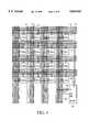
- FIG. 4is a schematic top plan view of a 4 ⁇ 4 block of logic cells of the FPGA circuit of FIG. 1 with bussing network and RAM.
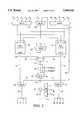
- FIG. 5is a schematic logic level circuit diagram of one logic cell of the FPGA circuit of FIG. 1.
- FIGS. 7 and 8are schematic logic level circuit diagrams of two alternate logic cell embodiments of an FPGA circuit of the present invention.
- FIGS. 9 and 10are schematic top plan views of portions of the FPGA circuit of FIG. 1 showing clock and reset signal distribution for the present invention.
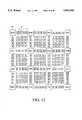
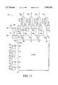
- FIG. 11is a schematic top plan view of four blocks of cells of FIG. 4, illustrating the staggered arrangement of repeater switch units in the FPGA circuit of the present invention.
- FIG. 12is a schematic top plan view of a 3 ⁇ 3 set of blocks of cells of the FPGA of FIGS. 1 and 4, illustrating the placement of dedicated function elements (DFE) such as RAM at corners of each block between rows and columns of repeaters.
- DFEdedicated function elements
- FIG. 13is a schematic logic level circuit diagram of a RAM and the RAM-bus interface for the FPGA circuit of the present invention.
- FIG. 14is a schematic top plan view of a portion of an FPGA circuit of the present invention containing eight blocks of logic cells and their associated RAM blocks, and showing an alternate RAM to bus network connection scheme from that shown in FIG. 4.
- FIG. 17is a schematic logic level circuit diagram of a corner logic cell of the FPGA and the cell-to-pad interface according to one embodiment of the present invention.
- FIG. 18is a partial schematic diagram of a set of logic cells at the perimeter of the FPGA circuit of FIG. 1, illustrating an alternative connectivity of such cells to I/O pads of the circuit from that shown in FIG. 16.
- FIGS. 20 and 21are schematic logic level circuit diagrams of cell-pad interfaces for two types of I/O pads according to a third connectivity embodiment.
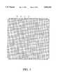
- Blocks 15 of logic cells 11need not have the same size over the entire FPGA device. For example, different quadrants of the device may contain 4 ⁇ 4, 6 ⁇ 6 or 8 ⁇ 8 square blocks or 4 ⁇ 6, 4 ⁇ 8, 6 ⁇ 8, 6 ⁇ 12 or 8 ⁇ 16 rectangular blocks, etc.
- each logic cellhas a set of B inputs (designated here as B n , B e , B s , B w ) receiving signals output by the respective B outputs of the four nearest neighbor cells.
- B n , B e , B s , B wB inputs
- Each logic cellalso has a set of A inputs (designated A n , A e , A s , A w ) receiving signals output by the respective A outputs of the four nearest neighbor cells in the same row or column as the receiving cell, and a set of B inputs (designated B nw , B ne , B se , B sw ) receiving signals output by the respective B outputs of the four diagonally adjacent neighboring cells.
- a inputsdesignated A n , A e , A s , A w
- B inputsdesignated B nw , B ne , B se , B sw
- FIG. 4shows the cell-to-bus connections in the FPGA circuit.
- the 4 ⁇ 4 group of logic cells 11 in a single blockhave bus lines distributed between the rows and columns of cells.
- Each set of three bus linesincludes one local bus line 23 and two express bus lines 25.
- Logic cells 11are directly connected only to the local bus lines 23, with access to the express bus lines 25 being indirect through the local bus lines at connective repeater units 27 located at the perimeter of each block of cells.
- one embodiment of a logic cell in the FPGA of the present inventionhas four sets of inputs, including those designated as A inputs (direct connections A n , A e , A s , A w from neighboring cells and a local bus input A L ), a second set designated as B inputs (direct connections B n , B e , B s , B w from the neighboring cells and a local bus input B L ), a third local bus input designated as C L , and a fourth local bus input designated as D L .
- the logic cellalso has three sets of outputs, including A outputs and B outputs connected to the respective A inputs and B inputs of the four neighboring cells, and also including a local bus output L.
- the A and B outputs and the direct A and B inputsare connected as described above with reference to FIG. 2.
- the local bus inputs (A L , B L , C L , D L ) and local bus output (L) of a cellare connected to the ten neighboring horizontal and vertical local bus lines 23 through connecting signal paths 29 as previously described with reference to FIG. 4 and in greater detail in the manner shown in FIG. 6.
- each of the local bus connecting signal paths (H0-H4 and V0-V4)pass through a corresponding pass gate 31 to one of five intermediate signal lines 33 0 -33 4 within the cell.
- Each intermediate signal line 33 0 -33 4can be coupled by the pass gates 31 to either of two local bus connecting signal paths, one of them from a corresponding vertical bus line (via paths V0-V4) and the other from a horizontal bus line (via paths H0-H4).
- each of these five intermediate signal lines 33 0 -33 4is connected to four bus input select multiplexers 35 A -35 D .
- each multiplexer 35 A-35 Dhas five inputs, one for each intermediate signal line 33 0 -33 4 .
- the output of each multiplexer 35 A -35 Dform the four local bus inputs (A L , B L , C L , D L ) of the cell.
- any one of the ten neighboring local bus lines to which the logic cell is connectedcan provide input signals to any one of the four local bus inputs, as configured by the pass gates 31 and the selections of the multiplexers 35 A-35 D .
- the local bus output L for the logic cellalso connects to the five intermediate signal lines 33 0 -33 4 through a set of pass gates 37.
- the output Lcan be connected to provide output signals to any of the ten neighboring local bus lines, as configured by the pass gates 37 and 31.
- the output Lcan be connected to both a horizontal bus line and a vertical bus line at the same time, by enabling both corresponding connecting pass gates 31.
- the userWhile usually, one of the intermediate signal lines 33 is selected by a pass gate 37 for use of the local bus output L and the other four intermediate signal lines 33 are selected by the multiplexers 35 A -35 D (and disabling the corresponding output pass gates 37) for receipt of local bus input signals, the user has the option of configuring the output pass gates 37 and input select multiplexers 35 A -35 D for providing a feedback path from the local bus output L to any of local bus inputs A L , B L or D L if extra feedback paths are needed. (As seen in FIG. 5, the internal cell structure already allows selection of feedback versus the C L local bus input by the multiplexer 39.)
- each logic cellmay include two 8-bit look-up tables (L.U.T.s) 45 and 47 that are addressed by the A, B and C inputs.
- the look-up tablestypically consist of static RAM memory cells that are operated as read-only memory, i.e., that are loaded during initial configuration of the FPGA device and are not dynamically reprogrammed during operation.
- the set of A inputs(A n , A e , A s , A w ,A L ) are received by a multiplexer 41 and one of them is selected.
- the selected output of this A multiplexeris connected to the a 0 address input of the first L.U.T. 45 and the a 1 address input of the second L.U.T.
- the set of B inputs(B n , B e , B s , B w , B L ) are likewise selected by a B input select multiplexer 43 and the selected output is connected to the a 0 address input of the second L.U.T. 47 and the a 1 address input of the first L.U.T. 45.
- a third multiplexer 39receives the local bus input C L and an internal feedback signal on the feedback line 40, and outputs one of them to the a 2 address inputs of the first and second L.U.T.s 45 and 47.
- the logic celluses the two 8-bit look-up tables 45 and 47 to provide a wide variety of combinatorial logic.
- the outputs 49 and 51 of the look-up tables 45 and 47branch into a number of signal paths leading both to the cell's A and B outputs and to the local bus output L.
- the L.U.T. outputs 49 and 51are connected to respective data lines 52 and 53 which may be coupled by respective first and second output multiplexers 54 and 55 to the output lines 56 and 57 providing output signals to the respective A and B outputs.
- the L.U.T. outputs 49 and 51also connect to respective second data lines 59 and 60 leading to yet a third output multiplexer 61.
- the control signal for the multiplexer 61is derived from the local bus input D L or from a fixed logic level signal ("0" or "1") as selected by a multiplexer 62.
- the selected third multiplexer output 63is split into two parallel paths, one a combinatorial or nonregistered path 65, the other a registered path containing a flip-flop 66.
- a fourth output multiplexer 67connects one of those two paths to its output 69.
- the fourth multiplexer output 69also splits into several parallel paths.
- One of these paths 70leads to the first output multiplexer 54 for possible selection and coupling to the A outputs of the cell, and another of these paths 71 leads to the second output multiplexer 55 for possible selection and coupling to the B outputs of the cell.
- a third pathleads through an output buffer 73 to an output line 75 providing output signals to the cell's local bus output L.
- the output buffer 73may be a tristate buffer controlled by an enable signal provided by yet another multiplexer 74. Selectable options include a logic "1" signal in which the buffer 73 is always enabled and two dynamic output enable signals OE H and OE V received from dedicated bus lines.
- a fourth path for the fourth multiplexer output 69is a feedback path 40 leading to the input multiplexer 39 for possible selection in place of local bus input C L .
- the cell's structuregives it considerable flexibility, while maintaining relative simplicity and compact size.
- the A and B input multiplexers 41 and 43provide complete symmetry with respect to the four nearest neighbor cells.
- the local bus input circuitry of FIG. 6provides complete identity of options for all ten of the cell's local bus connections.
- the A and B outputsare provided with matching options.
- the A outputscan be provided with the output of the first look-up table 45, either nonregistered via direct signal line 52 or registered via the second signal line 59, the register 66 and signal line 70. Or it can be provided with the output of the second look-up table 47, via the second signal line 60 and signal line 70, again either registered or nonregistered.
- the outputs of look-up tables 45' and 47'connect through output multiplexers 54' and 55' to respective A and B outputs of the logic cell.
- the tables 45' and 47'also connect to a third multiplexer 61' controlled by a fixed "0" or "1" control signal or by the local bus input D L , as selected by yet another multiplexer 62'.
- the two look-up tables 45' and 47'effectively combine into a single 16-bit table with local bus input D L acting as a fourth address input.
- the selected output of third multiplexer 61'connects to a registered/nonregistered selection circuit consisting of a nonregistered signal path 65', a flip-flop register 66' in a registered signal path, and a multiplexer 67' selecting one of these two signal paths.
- the resulting output 69'connects through multiplexers 54' and 55' to the cell's A and B outputs and through an output buffer 73' to the cell's local bus output L.
- the output buffer 73'may be a tristate buffer responsive to an output enable signal selected by a multiplexer 74'.
- FIG. 7also illustrates that the output buffer circuit 73' may also include output polarity control via yet another multiplexer 72'.
- the input multiplexers 41", 43" and 39"are connected to the A, B and C direct and local bus inputs, and the feedback line 40", and to the address inputs a 0 , a 1 , and a 2 of the SRAMs 45" and 47" in the same manner as in FIG. 5.
- the outputs 49" and 51" of the SRAMs 45" and 47"each split into a nonregistered path 64" and 65” and a registered path containing a flip-flop 66" and 68" that lead to output multiplexers 54" and 55", respectively.
- the selected output 69" from the output multiplexer 61"connects to a feedback line 40" leading to the input multiplexer 39" and also connects through a buffer 73" to a local bus output L.
- the buffer 73"may have output enable control from a local bus OE H or OE V via a multiplexer 74".
- the circuitry between the SRAM outputs 49" and 51" and the direct A and B outputs and local bus output Lmay be as in FIG. 5.
- the write access to the SRAMs 45" and 47" unique to this cell embodimentis provided by a DATA -- IN line 84" connected to the FPGA's bus network and to data inputs d 0 of the two SRAMs 45" and 47", by address inputs a 0 -a 2 , and by write enable circuitry providing a write enable signal WE to either of SRAMs 45" and 47".
- the write enable circuitryincludes two AND gates 76" and 77" with three inputs 78"-80" each and each with an output coupled to the write enable input to one of the SRAMs 45" and 47".
- One of the AND gate inputs 78"receives the same control signal selected by multiplexer 62" as the local bus output multiplexer 61".
- input 78"selectively receives either fixed logic low ("0") or high ("1") or dynamic local bus input signals D H or D V .
- the input 78"is inverted prior to arrival at AND gate 76" but is not inverted prior to arrival at the other AND gate 77".
- only one of the SRAMs 45" and 47”will receive a write enable signal at a time. If the input 78" is at a low logic level, the left SRAM 45" will be enabled, but if the input 78" is at a high logic level, the right SRAM 47” will be enabled.
- Use of the same control signal for the local bus output multiplexers 61"ensures that the data written from DATA -- IN line 84" can be verified at the local bus output L.
- FIG. 9shows clock distribution circuitry for an FPGA of the present invention.
- Other possible clock distribution arrangementsmay include some other number of clock lines, partially populating multiplexers 88, etc.
- Each column of logic cells 11may be provided with its own clock select multiplexer 88 having inputs respectively connected to some or all of the global clock lines CK0-CK7.
- the RESET signal provided by a global RESET line 114 to reset column lines 115may likewise have its polarity determined by sectors of logic cells by means of reset polarity-select and distribution-enable circuit 116 constructed in the same manner as the clock circuits 94.
- the logic cells 11are organized into 4 ⁇ 4 blocks 15 of cells, at the boundaries 13 of which are located a set of connecting switches, called “repeaters", 27, for the bus network.
- the bus networkincludes sets of horizontal bus lines 21 running between the rows of logic cells 11 and sets of vertical bus lines 19 running between the columns of logic cells 11.
- Each set of bus lines 19 or 21includes a local bus line 23 limited to a single block 15 of cells and two express bus lines 25 extending by means of the repeaters 27 through multiple blocks of cells. For simplicity, only one set of three bus lines 23 and 25 is shown for each row and column of cells 11. However, as also previously mentioned there are normally five sets of three bus lines 19 and 21 for each row and column of cells 11, as seen in FIG. 4.
- the repeaters 27allow local bus lines 23 to be connected to express bus lines 25. Only local bus lines connect directly to the logic cells 11.
- the repeaters 27have a staggered arrangement in which any one repeater 27 provides a selectable connection between a local bus line 23 and only one of the two express bus lines 25 in the set and in which successive repeaters 27 connect to alternate express bus lines in the set.
- each express bus line 25encounters a repeater 27 every eight rows or columns of cells 11 rather than every four rows or columns, while each local bus line 23 encounters a repeater 27 every four rows or columns of cells 11.
- Each local bus line 23 in a block 15 of cells 11is connectable to each of its corresponding express bus lines 25 at opposite ends of the block 15.
- DFEdedicated function elements 83
- RAMrandom access memory
- DFEdedicated function elements 83
- RAMrandom access memory
- dedicated or specialized circuitssuch as multipliers, shift registers, fixed-function digital or analog logic, microcontrollers, comparators, and analog-to-digital or digital-to-analog converters. Since the corner spaces naturally result from the block organization of the cells and their associated bussing and repeaters, the placement of dedicated logic of memory in such spaces comes at little or no cost in silicon area for the overall device.
- the input buffers 90are connected through flip-flops 93 to data lines 95 0 -95 3 .
- the output buffers 91are directly connected to the data lines 95 0 -95 3 .
- a write enable signal WEis received from a write enable line 96 via a flip-flop register 97.
- the register output Q of flip-flop 97connects via a first branch to a write enable input port of the SRAM 85 and via a second branch 99 through respective side branches 99 0 -99 3 to the tristate control inputs of input buffers 90 for each data port d 0 -d 3 .
- An output enable signal OEis also received from an output enable line 102 via a flip-flop register 103.
- the output 104 of register 103connects to a first input of an AND gate 101, while a third branch 100 of the output of flip-flop register 97 connects to a complementary second input of the AND gate 101.
- the output 105 of AND gate 101connects through respective side branches 105 0 -105 3 to the tristate control inputs of output buffers 91 for each data port d 0- d 3 .
- a 5-bit addressis synchronously received from the outputs of registers 87 at the address ports 9 0 -9 4 and a write enable signal is also synchronously received at the write enable port WE of the SRAM 85 via the first branch 98 from flip-flop register 97.
- the write enable signalalso enables the input buffers 90 via side branches 99 0 -99 3 and disables the output buffers 91 via AND gate 101 and side branches 105 0 -105 3 .
- data bits received on data lines 95 0 -95 3are transmitted through the input buffers 90 and data lines 89 0 -89 3 to the respective data ports d 0 -d 3 and written into the SRAM 85 at the address received at address ports a 0 -a 4 .
- an address and an output enable signal OEare synchronously received via registers 87 and 103 at address ports a 0 -a 4 and at AND gate 101, respectively.
- the write enable signal WE transmitted by register 97is low, disabling the input buffers 90 via branch lines 99 0 -99 3 and allowing the AND gate 101 to enable the output buffers 91 via branch lines 105 0 -105 3 .
- Data stored at the received addressis output through data ports d 0 -d 3 to data lines 95 0 -95 3 .
- the RAM block 83can be suitably modified so that the write enable and output enable signals are active low.
- the RAM block 83 of FIG. 13may be connected to the bus network such that each of the five address lines 86 are connected to a different one of the five vertical local bus lines 23 corresponding to one column of cells 11, the write enable and output enable lines 96 and 102 are connected to two vertical express bus lines 25 corresponding to that same column of cells, and each of the four data lines 95 are connected to a different horizontal local bus line corresponding to each of the four rows of cells 11 in the 4 ⁇ 4 group of cells adjacent that RAM block 83.
- Other connection schemesare also possible.
- FIG. 14shows eight of the 4 ⁇ 4 blocks 15 of logic cells 11, together with some of vertical and horizontal express bus lines 19 and 21 running between the rows and columns of cells 11 in and between the blocks 15. Turning switches 81 connect selected vertical and horizontal bus lines 19 and 21 to each other where they intersect. At the lower righthand corner of each block 15 of logic cells 11 is a RAM block 83. As seen in FIG. 14
- each RAMblock 83may be a dual port SRAM with a write enable port WE, write address ports A in and data input ports D in for write operations to the SRAM, and with a read enable port OE, separate read address ports A out and separate data output ports D out for reading data from the SRAM.
- write enable port WEwrite enable port
- OEread enable port
- a 6-bit write address(WRITE ADDR.) corresponding to a set of locations in RAM to which 8 data bits are to be written is received from the bus network or from external pads of the device.
- Two of the six bitsare seen to be input into a conventional 2-to-4 bit decoder 171.
- Decoder 171activates one and only one of its four outputs 173 depending on which of the four possible two-bit input values it receives.
- Each of the four decoder outputs 173is connected into an input of one of four OR gates 175.
- a global write enable signal WEis received at the other input of the four OR gates 175.
- the OR gate outputs 177connect to vertical express bus lines 19 corresponding to each of the four columns of blocks 15 and their corresponding columns of RAM blocks 83.
- the write enable port WE of these RAM blocksconnect to these particular vertical express bus lines to receive a decoded write enable signal from the corresponding OR gate outputs 177.
- one of the four columns of RAM blocks 83will be activated for a write operation if the global write enable signal WE is active.
- the other four write address bits in the 6-bit addressconnect to horizontal express bus lines 21 and then through turning switches 81 to vertical bus lines 19 connected to write address ports A in of each RAM block 83.
- Eight data input lines D in (0)-D in (7)connect through horizontal busses 19 adjacent to each row of logic cells 11 to the data input ports D in of the RAM blocks 83, with each RAM block 83 receiving four parallel data input signals from either D in (0)-D in (3) or D in (4)-D in (7).
- two rows of RAM blocksare needed to write single bytes of data to any given address.
- a 6-bit READ ADDRESSis provided with two of the address bits connecting to another 2-to-4 bit decoder 172 providing four outputs 174, one for each column of RAM, and with the four remaining address bits connecting through horizontal express bus lines 21 and turning switches 81 to vertical express bus lines 19 leading to read address ports of the RAM blocks 83.
- all eight RAM blocksare provided with four address bits, but only one column of RAM blocks are provided with a read enable signal derived from the two address bits input into the decoder 172.
- Eight data output lines D out (0)-D out (7)connect via horizontal express bus lines to the data output ports D out in two rows of RAM blocks 83.
- One valuable arrangementprovides mirror symmetry between the read and write address ports A in and A out in adjacent columns of RAM blocks 83. This reduces by approximately half the required number of vertical bus resources used for address signals when building a dual port RAM element. Note that in FIG. 14 the first two columns of RAM blocks share common read address lines 176. Likewise, the last two columns of RAM blocks share common read address lines 178. The second and third columns of RAM blocks share common write address lines 179. In larger groups of memory blocks, such as those with eight or sixteen columns of RAM blocks and 3-to-8 or 4-to-16 bit decoders, use of vertical bus resources would alternate from read address lines in one column of logic blocks 15 to write address lines in the next column of logic blocks 15.
- each block of logic cellscould also be specialized logic structures, such as multipliers.
- a 4 ⁇ 4 multipliercan be connected to the bus network in the same way as the dual-port SRAM seen in FIGS. 14 and 15, with one set of address inputs replaced by one four-bit operand and the other set of address inputs replaced by a second four-bit operand.
- the eight-bit product output of the multiplierreplaces the two four-bit data in and data out lines of the RAM.
- the logic cells 11 at the edge of the arraymay be connected to the input/output (I/O) pads 17 in any of a number of ways.
- One way shown hereconnects each logic cell, e.g. cell 112, to three neighboring I/O pads 117-119 via I/O lines 121-123 and also connects each I/O pad, e.g. pad 118, to three neighboring logic cells 111-113 via I/O lines 122, 124 and 125.
- An exception to this schemeusually occurs at the corners of the array and at the ends of the line of pads.
- the end pad 131connects to only two logic cells 134 and 135 via I/O lines 132 and 133.
- the corner logic cell 135connects to four I/O pads, namely pads 130 and 131 in one line of I/O pads and pads 139 and 140 in another line of pads, via I/O lines 132 and 136-138.
- Other arrangementsare possible.
- FIG. 17Connects for other logic cells and I/O pads are analogous.
- the particular logic cell 135 seen in FIG. 17is the lower righthand corner cell of the array, i.e. the cell in the bottom row and rightmost column in FIG. 1. As seen in FIG. 16, this particular cell 135 connects to the two rightmost I/O pads 139 and 140 in the bottom line of pads and to the two bottommost I/O pads 130 and 131 in the right line of pads of the circuit.
- the cell 135 in FIG. 17is connected like all of the other cells in the array to a set of adjacent vertical and horizontal bus lines 19 and 21, either directly to local buses 23 or indirectly to express buses 25 via the local buses 23 and repeatable switches 27. As in FIGS.
- the connections between the cell 135 and the 5 horizontal and 5 vertical local bus lines 23may be made via a set of ten bidirectional data bus lines 29.
- the corner cell 135also makes direct connections to the nearest neighbor cells (not shown) as in FIG. 2. However, because the cell 135 lacks neighbors to its right and below it, the four unused A and B direct inputs (A E , B E , A S and B S ) and the four unused A and B direct outputs (two A's and two B's) are used to facilitate the connections to the I/O pads, and to certain express bus lines 25.
- each of the 5 horizontal express lines 25 that does not encounter the end repeater units 27connects to a pair of 5-to-1 multiplexers 141 and 143 and a pair of five-element sets of switches 145 and 147.
- the 5 vertical express lines 25 that do not encounter end repeater units 27 terminating the column of bus linesare connected to multiplexers 142 and 144 and sets of switches 146 and 148.
- the outputs of multiplexers 141 and 142connect to respective direct B inputs B E and B S and also to output signal paths 153 and 154 leading to I/O pads.
- the outputs of multiplexers 143 and 144connect only to output signal paths 155 and 156 leading to I/O pads.
- the sets of switches 145 and 146connect the direct B outputs of the cell 135 to the 10 horizontal and vertical express lines 25 not terminated by repeaters 27.
- the sets of switches 147 and 148connect input signal paths 169 and 170 from I/O pads to the same 10 horizontal and vertical express lines 25.
- the input signal paths 169 and 170also connect to respective direct A inputs A E and A S of the cell 135.
- the right-side output signal paths 151, 153 and 155each go to the bottommost two pads 130 and 131 on the right line of pads and to the rightmost pad 139 on the bottom line of pads in FIG. 16.
- the bottom-side output signal paths 152, 154 and 156each go to the rightmost two pads 139 and 140 on the bottom line of pads and the bottommost pad 131 on the right line of pads in FIG. 16.
- each of the output signal paths 151-156is selectively connectable to any of three different pads from the four available pad connections.
- Signal paths 155 and 156may also be used to provide a tristate enable signal to an output buffer between the paths 151-154 and the I/O pads.
- the input signal paths 169 and 170are likewise connectable to the I/O pads.
- Conductive lines 161, 163 and 165connect to respective pads 130, 131 and 139, while conductive lines 162, 164 and 166 connect to respective pads 131, 139 and 140 seen in FIG. 16.
- the input select multiplexers 167 and 168each connect a selected conductive line 161-166 to the input signal paths 169 and 170.
- the number of I/O padscan be increased, from one pad 17 per perimeter logic cell 11 in FIG. 16, to three pads 17' per pair of perimeter logic cells 12 shown here, or even to as many as two pads per perimeter logic cell, if desired.
- the I/O pads 180, 181, 183, 184, etc., directly opposite one of the noncorner perimeter logic cells 187-190can be connected to three perimeter logic cells and to their associated bus lines as in FIG. 16.
- I/O pad 181is connectable to the perimeter logic cells 187-189 and associated bus lines as will be seen below with reference to FIG. 19.
- I/O pads 182, 185, etc.are indirectly connectable to the two nearest perimeter logic cells through the bus lines associated with them, as will be seen in FIG. 19.
- each noncorner perimeter logic cell 187-190, etc.is connectable to four I/O pads.
- cell 188is connectable to the I/O pads 180-183.
- Corner cells 191, etc.connect to six I/O pads 184-186 and 192-194, three from each line of pads.
- the I/O pad 181is connected to an input buffer 201, whose output 202 splits into three input lines 203-205 leading to direct cell inputs 206-208 of the logic cells 187-189.
- the buffer's output 202is also connectable, through programmable switches 209, to bidirectional signal lines 210-212 leading to repeater switch units 27 at the ends of horizontal bus lines 21 associated with each of three rows of logic cells that include the cells 187-189.
- an output multiplexer 213Associated with the I/O pad 181 is associated with the I/O pad 181.
- This multiplexer 213is connected to the bidirectional signal lines 210-212 from the three rows of horizontal bus lines 21 associated with the logic cells 187-189, and is also connected to cell output lines 214-216 coming from the direct cell outputs 217-219 of the logic cells 187-189.
- Each of these signal lines 210-212 and 217-219connects to the inputs of the multiplexer 213, which selects at most one of them for transmission through an output buffer 220 to the I/O pad 181.
- I/O pads 180 and 183 directly opposite cells 187 and 189are connected in a manner identical to I/O pad 181.
- I/O pad 182is located between I/O pads 181 and 183. While I/O pads 181 and 183 are positioned directly opposite perimeter logic cells 188 and 189, pad 182 is not positioned opposite any logic cell but rather is located opposite the space between the rows associated with cells 188 and 189 and containing the horizontal bus lines 21 associated with cell 189.
- the I/O pad 182is connected to an input buffer 221 whose output is connectable through programmable switches 222 to bidirectional signal lines 223 and 224. These signal lines 223 and 224 also couple through an output multiplexer 225 to an output buffer 226 connected to the I/O pad 182.
- the bidirectional signal lines 223 and 224connect to the signal lines 210 leading to and from the end repeater switch units 27 for the horizontal bus lines 21 associated with cells 188 and 189.
- FIGS. 20 and 21yet another embodiment of an input/output interface for FPGAs of the present invention is shown for two of the I/O pads 230 and 231.
- FIG. 20shows only the paths associated with one I/O pad 231 located immediately opposite a logic cell 228. The scheme is repeated for each cell 227, 228, 229, etc. around the perimeter of the matrix of cells in the FPGA device.
- FIG. 21shows only the paths associated with one I/O pad 230 located opposite a position between two logic cells 227 and 228. This scheme is also repeated around the perimeter of the FPGA, although usually these second I/O pads 230 are found only at every other available position between cells. Both types of I/O pads, those directly opposite logic cells and those opposite between cell positions are normally found together in an FPGA, as seen in the second I/O interface embodiment in FIG. 19.
- the I/O pads 231 and 230have pull-up transistors 232 and 252 whose gates are controlled by a user-configurable bit (PULL-UP).
- the primary function of these transistors 232 and 252is to provide a logical "1" to unused pads.
- a transistor 232 or 252is approximately equivalent to a 10K resistor to V cc .
- Each pad 231 and 230has an input buffer 234 and 254, respectively, connected thereto, and also has an output buffer 233 and 253, respectively, also connected thereto.
- the input buffers 234 and 254have a selectable threshold level, either TTL or CMOS, which is determined by a user-configurable bit (TTL/CMOS).
- the output buffers 233 and 253have selectable drive levels controlled by another user-configurable bit (HALF/FULL DRIVE).
- the drive levelsdiffer in their DC current sinking capabilities.
- the bufferscould have controllable slew rate, fast or slow, with the same full DC current sinking capability.
- An "OPEN COLLECTOR" configuration bitselectively enables or disables the active pull-up of the output buffer 233 or 253.
- the enable signal (TRI-STATE) for the tristate output buffers 233 and 253are selected by multiplexers 235 and 255 from a number of options.
- the optionstypically include fixed logic levels “0" and "1" in which the buffer is either always driving or never driving, and a number of dynamic signals generated in the array.
- the primary I/O pads 231 directly opposite a perimeter logic cell 228have three dynamic signal selections (CELL 1, CELL 2, CELL 3) associated with the three available output cells 227, 228 and 229, while the secondary I/O pads 230 located in a between-cell position have two dynamic signal selections (CELL 1, CELL 2) associated with its two available output cells 227 and 228.
- the dynamic signalsmay be generated within the respective cells themselves or may be provided by bus lines 247, 248 or 249 associated with those cells.
- the I/O pad 231connects through an output selection multiplexer 237 and the output buffer 233 to bus lines 247, 248 and 249 associated with three neighboring perimeter logic cells 227, 228 and 229 (designated CELL 1, CELL 2 and CELL 3 respectively) by way of lines 241-244. Note that two signal options are available from the bus lines 248 associated with the cell 228 immediately opposite the pad 231, while only one signal option is available from the neighboring bus lines 247 and 249.
- the output select multiplexer 237also receives a direct cell output 245 from logic cell 228.
- the I/O pad 231connects through input buffer 234 to a direct cell input 250 to logic cell 228 and also connects via user-configurable switches 251 to the same set of lines 241-244 leading to the bus lines 247-249.
- the pad 230 located opposite the position between cells 227 and 228connects through an output selection multiplexer 257 and output buffer 253 to bus lines 247 and 248 associated with the cells 227 and 228 by way of lines 261 and 262.
- the multiplexer 257also receives direct diagonal cell outputs 263 and 264 from the cells 227 and 228.
- the I/O pad 230connects through input buffer 254 to direct diagonal cell inputs 265 and 266 of cells 227 and 228 and also connects via user-configurable switches 267 to the lines 261 and 262 leading to the busses 247 and 248.
Landscapes
- Physics & Mathematics (AREA)
- Mathematical Physics (AREA)
- Engineering & Computer Science (AREA)
- General Engineering & Computer Science (AREA)
- Computer Hardware Design (AREA)
- Computing Systems (AREA)
- Computer Networks & Wireless Communication (AREA)
- Theoretical Computer Science (AREA)
- General Physics & Mathematics (AREA)
- Logic Circuits (AREA)
- Design And Manufacture Of Integrated Circuits (AREA)
- Static Random-Access Memory (AREA)
Abstract
Description
Claims (18)
Priority Applications (20)
| Application Number | Priority Date | Filing Date | Title |
|---|---|---|---|
| US08/650,477US5894565A (en) | 1996-05-20 | 1996-05-20 | Field programmable gate array with distributed RAM and increased cell utilization |
| DE69730254TDE69730254T2 (en) | 1996-05-20 | 1997-05-09 | FPGA with lookup tables |
| PCT/US1997/007924WO1997044730A1 (en) | 1996-05-20 | 1997-05-09 | Field programmable gate array with distributed ram and increased cell utilization |
| CN97190570ACN1105970C (en) | 1996-05-20 | 1997-05-09 | Field programmable gate array with distributed RAM and increased cell utilization |
| EP01107759AEP1150431B1 (en) | 1996-05-20 | 1997-05-09 | FPGA with look-up tables |
| DE69721343TDE69721343T2 (en) | 1996-05-20 | 1997-05-09 | FPGA with set / reset lines |
| DE69711159TDE69711159T2 (en) | 1996-05-20 | 1997-05-09 | USER PROGRAMMABLE LOGICAL FIELD WITH DISTRIBUTED RAM AND INCREASED CELL USE |
| HK98112366.4AHK1011227B (en) | 1996-05-20 | 1997-05-09 | Field programmable gate array with distributed ram |
| EP01107756AEP1158402B1 (en) | 1996-05-20 | 1997-05-09 | FPGA with column set/reset lines |
| EP97926441AEP0846289B1 (en) | 1996-05-20 | 1997-05-09 | Field programmable gate array with distributed ram and increased cell utilization |
| EP01107758AEP1158403B1 (en) | 1996-05-20 | 1997-05-09 | FPGA with configurable clock lines |
| DE69721344TDE69721344T2 (en) | 1996-05-20 | 1997-05-09 | FPGA with configurable clock lines |
| KR10-1998-0700335AKR100429063B1 (en) | 1996-05-20 | 1997-05-09 | Field programmable gate array with distributed ram and increased cell utilization |
| EP01107760AEP1143336B1 (en) | 1996-05-20 | 1997-05-09 | FPGA with increased cell utilization |
| DE69721342TDE69721342T2 (en) | 1996-05-20 | 1997-05-09 | FPGA with increased cell usage |
| JP9542458AJPH11510038A (en) | 1996-05-20 | 1997-05-09 | Field programmable gate array having distributed RAM and increased cell utilization |
| US08/937,105US6014509A (en) | 1996-05-20 | 1997-09-24 | Field programmable gate array having access to orthogonal and diagonal adjacent neighboring cells |
| US08/936,334US6026227A (en) | 1996-05-20 | 1997-09-24 | FPGA logic cell internal structure including pair of look-up tables |
| US09/078,409US6167559A (en) | 1996-05-20 | 1998-05-13 | FPGA structure having main, column and sector clock lines |
| US09/650,979US6292021B1 (en) | 1996-05-20 | 2000-08-29 | FPGA structure having main, column and sector reset lines |
Applications Claiming Priority (1)
| Application Number | Priority Date | Filing Date | Title |
|---|---|---|---|
| US08/650,477US5894565A (en) | 1996-05-20 | 1996-05-20 | Field programmable gate array with distributed RAM and increased cell utilization |
Related Child Applications (3)
| Application Number | Title | Priority Date | Filing Date |
|---|---|---|---|
| US08/936,334DivisionUS6026227A (en) | 1996-05-20 | 1997-09-24 | FPGA logic cell internal structure including pair of look-up tables |
| US08/937,105DivisionUS6014509A (en) | 1996-05-20 | 1997-09-24 | Field programmable gate array having access to orthogonal and diagonal adjacent neighboring cells |
| US09/078,409DivisionUS6167559A (en) | 1996-05-20 | 1998-05-13 | FPGA structure having main, column and sector clock lines |
Publications (1)
| Publication Number | Publication Date |
|---|---|
| US5894565Atrue US5894565A (en) | 1999-04-13 |
Family
ID=24609080
Family Applications (5)
| Application Number | Title | Priority Date | Filing Date |
|---|---|---|---|
| US08/650,477Expired - LifetimeUS5894565A (en) | 1996-05-20 | 1996-05-20 | Field programmable gate array with distributed RAM and increased cell utilization |
| US08/937,105Expired - LifetimeUS6014509A (en) | 1996-05-20 | 1997-09-24 | Field programmable gate array having access to orthogonal and diagonal adjacent neighboring cells |
| US08/936,334Expired - LifetimeUS6026227A (en) | 1996-05-20 | 1997-09-24 | FPGA logic cell internal structure including pair of look-up tables |
| US09/078,409Expired - LifetimeUS6167559A (en) | 1996-05-20 | 1998-05-13 | FPGA structure having main, column and sector clock lines |
| US09/650,979Expired - LifetimeUS6292021B1 (en) | 1996-05-20 | 2000-08-29 | FPGA structure having main, column and sector reset lines |
Family Applications After (4)
| Application Number | Title | Priority Date | Filing Date |
|---|---|---|---|
| US08/937,105Expired - LifetimeUS6014509A (en) | 1996-05-20 | 1997-09-24 | Field programmable gate array having access to orthogonal and diagonal adjacent neighboring cells |
| US08/936,334Expired - LifetimeUS6026227A (en) | 1996-05-20 | 1997-09-24 | FPGA logic cell internal structure including pair of look-up tables |
| US09/078,409Expired - LifetimeUS6167559A (en) | 1996-05-20 | 1998-05-13 | FPGA structure having main, column and sector clock lines |
| US09/650,979Expired - LifetimeUS6292021B1 (en) | 1996-05-20 | 2000-08-29 | FPGA structure having main, column and sector reset lines |
Country Status (7)
| Country | Link |
|---|---|
| US (5) | US5894565A (en) |
| EP (5) | EP1158403B1 (en) |
| JP (1) | JPH11510038A (en) |
| KR (1) | KR100429063B1 (en) |
| CN (1) | CN1105970C (en) |
| DE (5) | DE69721343T2 (en) |
| WO (1) | WO1997044730A1 (en) |
Cited By (107)
| Publication number | Priority date | Publication date | Assignee | Title |
|---|---|---|---|---|
| US6020756A (en)* | 1998-03-03 | 2000-02-01 | Xilinx, Inc. | Multiplexer enhanced configurable logic block |
| US6034545A (en)* | 1998-01-30 | 2000-03-07 | Arm Limited | Macrocell for data processing circuit |
| US6069490A (en)* | 1997-12-02 | 2000-05-30 | Xilinx, Inc. | Routing architecture using a direct connect routing mesh |
| US6144220A (en)* | 1996-09-03 | 2000-11-07 | Xilinx, Inc. | FPGA Architecture using multiplexers that incorporate a logic gate |
| US6150841A (en)* | 1999-06-06 | 2000-11-21 | Lattice Semiconductor Corporation | Enhanced macrocell module for high density CPLD architectures |
| US6160419A (en)* | 1997-11-03 | 2000-12-12 | Altera Corporation | Programmable logic architecture incorporating a content addressable embedded array block |
| US6198304B1 (en)* | 1998-02-23 | 2001-03-06 | Xilinx, Inc. | Programmable logic device |
| US6242814B1 (en)* | 1998-07-31 | 2001-06-05 | Lsi Logic Corporation | Universal I/O pad structure for in-line or staggered wire bonding or arrayed flip-chip assembly |
| US6262595B1 (en)* | 1997-06-10 | 2001-07-17 | Altera Corporation | High-speed programmable interconnect |
| US6294927B1 (en)* | 2000-06-16 | 2001-09-25 | Chip Express (Israel) Ltd | Configurable cell for customizable logic array device |
| US20020108006A1 (en)* | 2000-10-26 | 2002-08-08 | Warren Snyder | Microcontroller programmable system on a chip |
| WO2002103908A1 (en)* | 2001-06-20 | 2002-12-27 | Telefonaktiebolaget Lm Ericsson (Publ) | Upgrading field programmable gate arrays overs data-communication networks |
| US6624658B2 (en)* | 1999-02-04 | 2003-09-23 | Advantage Logic, Inc. | Method and apparatus for universal program controlled bus architecture |
| US6744278B1 (en)* | 2000-09-02 | 2004-06-01 | Actel Corporation | Tileable field-programmable gate array architecture |
| US20050086649A1 (en)* | 2001-08-16 | 2005-04-21 | Martin Vorbach | Method for the translation of programs for reconfigurable architectures |
| US20060157833A1 (en)* | 2004-12-13 | 2006-07-20 | Hiromitsu Mashita | Semiconductor device, method for making pattern layout, method for making mask pattern, method for making layout, method for manufacturing photo mask, photo mask, and method for manufacturing semiconductor device |
| US20070150637A1 (en)* | 2002-02-18 | 2007-06-28 | Martin Vorbach | Bus systems and method for reconfiguration |
| US7389487B1 (en)* | 1998-04-28 | 2008-06-17 | Actel Corporation | Dedicated interface architecture for a hybrid integrated circuit |
| US20080191739A1 (en)* | 1996-09-04 | 2008-08-14 | Pani Peter M | Method and apparatus for universal program controlled bus architecture |
| US20080276030A1 (en)* | 1998-03-16 | 2008-11-06 | Actel Corporation | Sram bus architecture and interconnect to an fpga |
| CN100495696C (en)* | 2005-11-17 | 2009-06-03 | 中国科学院电子学研究所 | Symmetrical Wiring Channels for Programmable Logic Devices |
| US20090144485A1 (en)* | 1996-12-27 | 2009-06-04 | Martin Vorbach | Process for automatic dynamic reloading of data flow processors (dfps) and units with two- or three-dimensional programmable cell architectures (fpgas, dpgas, and the like) |
| US7571395B1 (en)* | 2005-08-03 | 2009-08-04 | Xilinx, Inc. | Generation of a circuit design from a command language specification of blocks in matrix form |
| US20090199167A1 (en)* | 2006-01-18 | 2009-08-06 | Martin Vorbach | Hardware Definition Method |
| US20100002485A1 (en)* | 2005-12-30 | 2010-01-07 | Micron Technology, Inc. | Configurable inputs and outputs for memory stacking system and method |
| US20100039139A1 (en)* | 2002-09-06 | 2010-02-18 | Martin Vorbach | Reconfigurable sequencer structure |
| US7702616B1 (en) | 2006-06-21 | 2010-04-20 | Actuate Corporation | Methods and apparatus for processing a query joining tables stored at different data sources |
| US7720838B1 (en)* | 2006-06-21 | 2010-05-18 | Actuate Corporation | Methods and apparatus for joining tables from different data sources |
| US7737724B2 (en) | 2007-04-17 | 2010-06-15 | Cypress Semiconductor Corporation | Universal digital block interconnection and channel routing |
| US7759972B1 (en)* | 2007-10-31 | 2010-07-20 | Altera Corporation | Integrated circuit architectures with heterogeneous high-speed serial interface circuitry |
| US7761845B1 (en) | 2002-09-09 | 2010-07-20 | Cypress Semiconductor Corporation | Method for parameterizing a user module |
| US7765095B1 (en) | 2000-10-26 | 2010-07-27 | Cypress Semiconductor Corporation | Conditional branching in an in-circuit emulation system |
| US7770113B1 (en) | 2001-11-19 | 2010-08-03 | Cypress Semiconductor Corporation | System and method for dynamically generating a configuration datasheet |
| US20100199069A1 (en)* | 2009-02-03 | 2010-08-05 | Won-Sub Kim | Scheduler of reconfigurable array, method of scheduling commands, and computing apparatus |
| US7774190B1 (en) | 2001-11-19 | 2010-08-10 | Cypress Semiconductor Corporation | Sleep and stall in an in-circuit emulation system |
| US7822968B2 (en) | 1996-12-09 | 2010-10-26 | Martin Vorbach | Circuit having a multidimensional structure of configurable cells that include multi-bit-wide inputs and outputs |
| US7825688B1 (en) | 2000-10-26 | 2010-11-02 | Cypress Semiconductor Corporation | Programmable microcontroller architecture(mixed analog/digital) |
| US7840842B2 (en) | 2001-09-03 | 2010-11-23 | Martin Vorbach | Method for debugging reconfigurable architectures |
| US7844437B1 (en) | 2001-11-19 | 2010-11-30 | Cypress Semiconductor Corporation | System and method for performing next placements and pruning of disallowed placements for programming an integrated circuit |
| US7844796B2 (en) | 2001-03-05 | 2010-11-30 | Martin Vorbach | Data processing device and method |
| US20110026519A1 (en)* | 2009-05-09 | 2011-02-03 | Cypress Semiconductor Corporation | Dynamically reconfigurable analog routing circuits and methods for system on a chip |
| US7893724B2 (en) | 2004-03-25 | 2011-02-22 | Cypress Semiconductor Corporation | Method and circuit for rapid alignment of signals |
| US7899962B2 (en) | 1996-12-20 | 2011-03-01 | Martin Vorbach | I/O and memory bus system for DFPs and units with two- or multi-dimensional programmable cell architectures |
| WO2011029037A1 (en)* | 2009-09-04 | 2011-03-10 | Integrated Device Technology, Inc. | Method and apparatus for compression of configuration bitstream of field programmable logic |
| US7917875B1 (en)* | 2005-08-04 | 2011-03-29 | Freescale Semiconductor, Inc. | Clock tree adjustable buffer |
| US20110145547A1 (en)* | 2001-08-10 | 2011-06-16 | Martin Vorbach | Reconfigurable elements |
| US20110215834A1 (en)* | 2010-03-05 | 2011-09-08 | Xilinx, Inc. | Programmable integrated circuit with mirrored interconnect structure |
| US8026739B2 (en) | 2007-04-17 | 2011-09-27 | Cypress Semiconductor Corporation | System level interconnect with programmable switching |
| US8040266B2 (en) | 2007-04-17 | 2011-10-18 | Cypress Semiconductor Corporation | Programmable sigma-delta analog-to-digital converter |
| US8049569B1 (en) | 2007-09-05 | 2011-11-01 | Cypress Semiconductor Corporation | Circuit and method for improving the accuracy of a crystal-less oscillator having dual-frequency modes |
| US8058899B2 (en) | 2000-10-06 | 2011-11-15 | Martin Vorbach | Logic cell array and bus system |
| US8069436B2 (en) | 2004-08-13 | 2011-11-29 | Cypress Semiconductor Corporation | Providing hardware independence to automate code generation of processing device firmware |
| US8067948B2 (en) | 2006-03-27 | 2011-11-29 | Cypress Semiconductor Corporation | Input/output multiplexer bus |
| US8069405B1 (en) | 2001-11-19 | 2011-11-29 | Cypress Semiconductor Corporation | User interface for efficiently browsing an electronic document using data-driven tabs |
| US8069428B1 (en) | 2001-10-24 | 2011-11-29 | Cypress Semiconductor Corporation | Techniques for generating microcontroller configuration information |
| US8078970B1 (en) | 2001-11-09 | 2011-12-13 | Cypress Semiconductor Corporation | Graphical user interface with user-selectable list-box |
| US8078894B1 (en) | 2007-04-25 | 2011-12-13 | Cypress Semiconductor Corporation | Power management architecture, method and configuration system |
| US8085067B1 (en) | 2005-12-21 | 2011-12-27 | Cypress Semiconductor Corporation | Differential-to-single ended signal converter circuit and method |
| US8085100B2 (en) | 2005-02-04 | 2011-12-27 | Cypress Semiconductor Corporation | Poly-phase frequency synthesis oscillator |
| US8089461B2 (en) | 2005-06-23 | 2012-01-03 | Cypress Semiconductor Corporation | Touch wake for electronic devices |
| US8092083B2 (en) | 2007-04-17 | 2012-01-10 | Cypress Semiconductor Corporation | Temperature sensor with digital bandgap |
| US8099618B2 (en) | 2001-03-05 | 2012-01-17 | Martin Vorbach | Methods and devices for treating and processing data |
| US8103496B1 (en) | 2000-10-26 | 2012-01-24 | Cypress Semicondutor Corporation | Breakpoint control in an in-circuit emulation system |
| US8103497B1 (en) | 2002-03-28 | 2012-01-24 | Cypress Semiconductor Corporation | External interface for event architecture |
| US8120408B1 (en) | 2005-05-05 | 2012-02-21 | Cypress Semiconductor Corporation | Voltage controlled oscillator delay cell and method |
| US8130025B2 (en) | 2007-04-17 | 2012-03-06 | Cypress Semiconductor Corporation | Numerical band gap |
| US8149048B1 (en) | 2000-10-26 | 2012-04-03 | Cypress Semiconductor Corporation | Apparatus and method for programmable power management in a programmable analog circuit block |
| US8156284B2 (en) | 2002-08-07 | 2012-04-10 | Martin Vorbach | Data processing method and device |
| US8160864B1 (en) | 2000-10-26 | 2012-04-17 | Cypress Semiconductor Corporation | In-circuit emulator and pod synchronized boot |
| US8209653B2 (en) | 2001-09-03 | 2012-06-26 | Martin Vorbach | Router |
| US8217700B1 (en)* | 2008-07-01 | 2012-07-10 | Cypress Semiconductor Corporation | Multifunction input/output circuit |
| US8230411B1 (en) | 1999-06-10 | 2012-07-24 | Martin Vorbach | Method for interleaving a program over a plurality of cells |
| US8281108B2 (en) | 2002-01-19 | 2012-10-02 | Martin Vorbach | Reconfigurable general purpose processor having time restricted configurations |
| US8281265B2 (en) | 2002-08-07 | 2012-10-02 | Martin Vorbach | Method and device for processing data |
| US8286125B2 (en) | 2004-08-13 | 2012-10-09 | Cypress Semiconductor Corporation | Model for a hardware device-independent method of defining embedded firmware for programmable systems |
| US8301872B2 (en) | 2000-06-13 | 2012-10-30 | Martin Vorbach | Pipeline configuration protocol and configuration unit communication |
| US20120326749A1 (en)* | 2009-12-14 | 2012-12-27 | Ecole Centrale De Lyon | Interconnected array of logic cells reconfigurable with intersecting interconnection topology |
| US8402313B1 (en) | 2002-05-01 | 2013-03-19 | Cypress Semiconductor Corporation | Reconfigurable testing system and method |
| US8441298B1 (en)* | 2008-07-01 | 2013-05-14 | Cypress Semiconductor Corporation | Analog bus sharing using transmission gates |
| USRE44365E1 (en) | 1997-02-08 | 2013-07-09 | Martin Vorbach | Method of self-synchronization of configurable elements of a programmable module |
| US8499270B1 (en) | 2007-04-25 | 2013-07-30 | Cypress Semiconductor Corporation | Configuration of programmable IC design elements |
| US8516025B2 (en) | 2007-04-17 | 2013-08-20 | Cypress Semiconductor Corporation | Clock driven dynamic datapath chaining |
| US8533677B1 (en) | 2001-11-19 | 2013-09-10 | Cypress Semiconductor Corporation | Graphical user interface for dynamically reconfiguring a programmable device |
| US8558578B1 (en) | 2009-05-05 | 2013-10-15 | Cypress Semiconductor Corporation | Programmable input/output circuit |
| US8686549B2 (en) | 2001-09-03 | 2014-04-01 | Martin Vorbach | Reconfigurable elements |
| WO2014123616A1 (en)* | 2013-02-08 | 2014-08-14 | The Trustees Of Princeton University | Fine-grain dynamically reconfigurable fpga architecture |
| US8812820B2 (en) | 2003-08-28 | 2014-08-19 | Pact Xpp Technologies Ag | Data processing device and method |
| US8819505B2 (en) | 1997-12-22 | 2014-08-26 | Pact Xpp Technologies Ag | Data processor having disabled cores |
| US8914590B2 (en) | 2002-08-07 | 2014-12-16 | Pact Xpp Technologies Ag | Data processing method and device |
| US9037807B2 (en) | 2001-03-05 | 2015-05-19 | Pact Xpp Technologies Ag | Processor arrangement on a chip including data processing, memory, and interface elements |
| US9092595B2 (en) | 1997-10-08 | 2015-07-28 | Pact Xpp Technologies Ag | Multiprocessor having associated RAM units |
| US9141390B2 (en) | 2001-03-05 | 2015-09-22 | Pact Xpp Technologies Ag | Method of processing data with an array of data processors according to application ID |
| US9170812B2 (en) | 2002-03-21 | 2015-10-27 | Pact Xpp Technologies Ag | Data processing system having integrated pipelined array data processor |
| US9250908B2 (en) | 2001-03-05 | 2016-02-02 | Pact Xpp Technologies Ag | Multi-processor bus and cache interconnection system |
| US20160070849A1 (en)* | 2014-09-09 | 2016-03-10 | International Business Machines Corporation | Critical region identification |
| US9330041B1 (en)* | 2012-02-17 | 2016-05-03 | Netronome Systems, Inc. | Staggered island structure in an island-based network flow processor |
| US9436631B2 (en) | 2001-03-05 | 2016-09-06 | Pact Xpp Technologies Ag | Chip including memory element storing higher level memory data on a page by page basis |
| US9448964B2 (en) | 2009-05-04 | 2016-09-20 | Cypress Semiconductor Corporation | Autonomous control in a programmable system |
| US20160358653A1 (en)* | 2015-06-08 | 2016-12-08 | Altera Corporation | Hardware programmable device with integrated search engine |
| US9552047B2 (en) | 2001-03-05 | 2017-01-24 | Pact Xpp Technologies Ag | Multiprocessor having runtime adjustable clock and clock dependent power supply |
| US9564902B2 (en) | 2007-04-17 | 2017-02-07 | Cypress Semiconductor Corporation | Dynamically configurable and re-configurable data path |
| US9720805B1 (en) | 2007-04-25 | 2017-08-01 | Cypress Semiconductor Corporation | System and method for controlling a target device |
| US9952282B1 (en) | 2009-05-05 | 2018-04-24 | Cypress Semiconductor Corporation | Combined analog architecture and functionality in a mixed-signal array |
| US10031733B2 (en) | 2001-06-20 | 2018-07-24 | Scientia Sol Mentis Ag | Method for processing data |
| US10698662B2 (en) | 2001-11-15 | 2020-06-30 | Cypress Semiconductor Corporation | System providing automatic source code generation for personalization and parameterization of user modules |
| US10911038B1 (en) | 2012-07-18 | 2021-02-02 | Netronome Systems, Inc. | Configuration mesh data bus and transactional memories in a multi-processor integrated circuit |
| US11043823B2 (en)* | 2017-04-06 | 2021-06-22 | Tesla, Inc. | System and method for facilitating conditioning and testing of rechargeable battery cells |
Families Citing this family (103)
| Publication number | Priority date | Publication date | Assignee | Title |
|---|---|---|---|---|
| US5943242A (en) | 1995-11-17 | 1999-08-24 | Pact Gmbh | Dynamically reconfigurable data processing system |
| KR19990071991A (en)* | 1996-10-10 | 1999-09-27 | 파레 호세 마리아 인센서 | Process for prototyping of mixed-signal applications and field programmable systems on chip for application of these processes |
| US6338106B1 (en) | 1996-12-20 | 2002-01-08 | Pact Gmbh | I/O and memory bus system for DFPS and units with two or multi-dimensional programmable cell architectures |
| DE19654846A1 (en)* | 1996-12-27 | 1998-07-09 | Pact Inf Tech Gmbh | Process for the independent dynamic reloading of data flow processors (DFPs) as well as modules with two- or multi-dimensional programmable cell structures (FPGAs, DPGAs, etc.) |
| DE19704728A1 (en) | 1997-02-08 | 1998-08-13 | Pact Inf Tech Gmbh | Method for self-synchronization of configurable elements of a programmable module |
| DE19704742A1 (en)* | 1997-02-11 | 1998-09-24 | Pact Inf Tech Gmbh | Internal bus system for DFPs, as well as modules with two- or multi-dimensional programmable cell structures, for coping with large amounts of data with high networking effort |
| US6185724B1 (en)* | 1997-12-02 | 2001-02-06 | Xilinx, Inc. | Template-based simulated annealing move-set that improves FPGA architectural feature utilization |
| US6202194B1 (en)* | 1997-12-11 | 2001-03-13 | Intrinsity, Inc. | Method and apparatus for routing 1 of N signals |
| DE19807872A1 (en) | 1998-02-25 | 1999-08-26 | Pact Inf Tech Gmbh | Method of managing configuration data in data flow processors |
| DE19810294A1 (en)* | 1998-03-10 | 1999-09-16 | Bayerische Motoren Werke Ag | Data bus for several subscribers that exchange data messages via at least one electrical cable e.g. in vehicle |
| US6204686B1 (en)* | 1998-12-16 | 2001-03-20 | Vantis Corporation | Methods for configuring FPGA's having variable grain blocks and shared logic for providing symmetric routing of result output to differently-directed and tristateable interconnect resources |
| JP3616518B2 (en) | 1999-02-10 | 2005-02-02 | 日本電気株式会社 | Programmable device |
| US6407576B1 (en) | 1999-03-04 | 2002-06-18 | Altera Corporation | Interconnection and input/output resources for programmable logic integrated circuit devices |
| WO2000052826A2 (en)* | 1999-03-04 | 2000-09-08 | Altera Corporation | Interconnection and input/output resources for programmable logic integrated circuit devices |
| AU4992300A (en)* | 1999-05-07 | 2000-11-21 | Morphics Technology, Inc. | Apparatus and method for programmable datapath arithmetic arrays |
| US6360348B1 (en)* | 1999-08-27 | 2002-03-19 | Motorola, Inc. | Method and apparatus for coding and decoding data |
| US6215327B1 (en)* | 1999-09-01 | 2001-04-10 | The United States Of America As Represented By The Secretary Of The Air Force | Molecular field programmable gate array |
| US6438737B1 (en)* | 2000-02-15 | 2002-08-20 | Intel Corporation | Reconfigurable logic for a computer |
| US6256253B1 (en)* | 2000-02-18 | 2001-07-03 | Infineon Technologies North America Corp. | Memory device with support for unaligned access |
| US6769109B2 (en)* | 2000-02-25 | 2004-07-27 | Lightspeed Semiconductor Corporation | Programmable logic array embedded in mask-programmed ASIC |
| US6694491B1 (en) | 2000-02-25 | 2004-02-17 | Lightspeed Semiconductor Corporation | Programmable logic array embedded in mask-programmed ASIC |
| US20010025363A1 (en)* | 2000-03-24 | 2001-09-27 | Cary Ussery | Designer configurable multi-processor system |
| US6661812B1 (en)* | 2000-04-05 | 2003-12-09 | Triscend Corporation | Bidirectional bus for use as an interconnect routing resource |
| WO2001093426A1 (en)* | 2000-05-30 | 2001-12-06 | Koninklijke Philips Electronics N.V. | Integrated circuit with a matrix of programmable logic cells |
| US7055125B2 (en)* | 2000-09-08 | 2006-05-30 | Lightspeed Semiconductor Corp. | Depopulated programmable logic array |
| US20020089348A1 (en)* | 2000-10-02 | 2002-07-11 | Martin Langhammer | Programmable logic integrated circuit devices including dedicated processor components |
| AU2060002A (en) | 2000-10-06 | 2002-04-22 | Pact Inf Tech Gmbh | Method and device |
| US20040015899A1 (en)* | 2000-10-06 | 2004-01-22 | Frank May | Method for processing data |
| US6981090B1 (en)* | 2000-10-26 | 2005-12-27 | Cypress Semiconductor Corporation | Multiple use of microcontroller pad |
| US6892310B1 (en)* | 2000-10-26 | 2005-05-10 | Cypress Semiconductor Corporation | Method for efficient supply of power to a microcontroller |
| US6990555B2 (en)* | 2001-01-09 | 2006-01-24 | Pact Xpp Technologies Ag | Method of hierarchical caching of configuration data having dataflow processors and modules having two- or multidimensional programmable cell structure (FPGAs, DPGAs, etc.) |
| US7210129B2 (en) | 2001-08-16 | 2007-04-24 | Pact Xpp Technologies Ag | Method for translating programs for reconfigurable architectures |
| US20090210653A1 (en)* | 2001-03-05 | 2009-08-20 | Pact Xpp Technologies Ag | Method and device for treating and processing data |
| US7581076B2 (en) | 2001-03-05 | 2009-08-25 | Pact Xpp Technologies Ag | Methods and devices for treating and/or processing data |
| US20090300262A1 (en)* | 2001-03-05 | 2009-12-03 | Martin Vorbach | Methods and devices for treating and/or processing data |
| AU2002347560A1 (en)* | 2001-06-20 | 2003-01-02 | Pact Xpp Technologies Ag | Data processing method |
| DE10139610A1 (en)* | 2001-08-11 | 2003-03-06 | Daimler Chrysler Ag | Universal computer architecture |
| US7139292B1 (en)* | 2001-08-31 | 2006-11-21 | Cypress Semiconductor Corp. | Configurable matrix architecture |
| US6839886B2 (en)* | 2001-09-24 | 2005-01-04 | Broadcom Corporation | Method and apparatus for facilitating circuit design |
| DE10159480B4 (en)* | 2001-12-04 | 2006-05-24 | Daimlerchrysler Ag | control device |
| US7577822B2 (en)* | 2001-12-14 | 2009-08-18 | Pact Xpp Technologies Ag | Parallel task operation in processor and reconfigurable coprocessor configured based on information in link list including termination information for synchronization |
| AU2003214046A1 (en)* | 2002-01-18 | 2003-09-09 | Pact Xpp Technologies Ag | Method and device for partitioning large computer programs |
| EP1518186A2 (en)* | 2002-03-21 | 2005-03-30 | PACT XPP Technologies AG | Method and device for data processing |
| US6970967B2 (en)* | 2002-06-18 | 2005-11-29 | Texas Instruments Incorporated | Crossbar circuit having a plurality of repeaters forming different repeater arrangements |
| US20040199894A1 (en)* | 2002-07-23 | 2004-10-07 | Klein Robert C. | Interconnect structure for electrical devices |
| US20110238948A1 (en)* | 2002-08-07 | 2011-09-29 | Martin Vorbach | Method and device for coupling a data processing unit and a data processing array |
| US7782398B2 (en)* | 2002-09-04 | 2010-08-24 | Chan Thomas M | Display processor integrated circuit with on-chip programmable logic for implementing custom enhancement functions |
| US7202908B2 (en)* | 2002-09-04 | 2007-04-10 | Darien K. Wallace | Deinterlacer using both low angle and high angle spatial interpolation |
| US7136108B2 (en)* | 2002-09-04 | 2006-11-14 | Darien K. Wallace | Segment buffer loading in a deinterlacer |
| US7480010B2 (en)* | 2002-09-04 | 2009-01-20 | Denace Enterprise Co., L.L.C. | Customizable ASIC with substantially non-customizable portion that supplies pixel data to a mask-programmable portion in multiple color space formats |
| US6774670B1 (en)* | 2002-12-30 | 2004-08-10 | Actel Corporation | Intra-tile buffer system for a field programmable gate array |
| DE112004000026D2 (en)* | 2003-04-04 | 2006-06-14 | Pact Xpp Technologies Ag | Method and device for data processing |
| US6996785B1 (en) | 2003-04-25 | 2006-02-07 | Universal Network Machines, Inc . | On-chip packet-based interconnections using repeaters/routers |
| US6882555B2 (en)* | 2003-06-18 | 2005-04-19 | Lattice Semiconductor Corporation | Bi-directional buffering for memory data lines |
| JP4334541B2 (en)* | 2003-07-16 | 2009-09-30 | イノテック株式会社 | Semiconductor integrated circuit |
| US7306977B1 (en)* | 2003-08-29 | 2007-12-11 | Xilinx, Inc. | Method and apparatus for facilitating signal routing within a programmable logic device |
| DE102004056322B4 (en)* | 2003-11-21 | 2012-07-19 | Infineon Technologies Ag | Logic Ground Cell and Logic Ground Cell Arrangement |
| US7167022B1 (en)* | 2004-03-25 | 2007-01-23 | Altera Corporation | Omnibus logic element including look up table based logic elements |
| WO2011061099A1 (en)* | 2004-04-02 | 2011-05-26 | Panasonic Corporation | Reset/load and signal distribution network |
| DE102004021047B3 (en)* | 2004-04-29 | 2005-10-06 | Koenig & Bauer Ag | Method for comparing an image with at least one reference image |
| US7243329B2 (en) | 2004-07-02 | 2007-07-10 | Altera Corporation | Application-specific integrated circuit equivalents of programmable logic and associated methods |
| JP2006053687A (en)* | 2004-08-10 | 2006-02-23 | Sony Corp | Arithmetic unit |
| JP2008530642A (en)* | 2005-02-07 | 2008-08-07 | ペーアーツェーテー イクスペーペー テクノロジーズ アクチエンゲゼルシャフト | Low latency mass parallel data processor |
| JP2006285572A (en)* | 2005-03-31 | 2006-10-19 | Toshiba Corp | Layout method of semiconductor integrated circuit |
| TWI321841B (en)* | 2005-04-29 | 2010-03-11 | Taiwan Semiconductor Mfg | System on chip development with reconfigurable multi-project wafer technology |
| WO2007062327A2 (en)* | 2005-11-18 | 2007-05-31 | Ideal Industries, Inc. | Releasable wire connector |
| WO2007060738A1 (en)* | 2005-11-28 | 2007-05-31 | Taiyo Yuden Co., Ltd. | Semiconductor device |
| US8352242B2 (en)* | 2006-02-21 | 2013-01-08 | Mentor Graphics Corporation | Communication scheme between programmable sub-cores in an emulation environment |
| EP2048784A4 (en)* | 2006-07-27 | 2010-10-27 | Panasonic Corp | INTEGRATED SEMICONDUCTOR CIRCUIT, PROGRAM CONVERTING APPARATUS, AND MAPPING APPARATUS |
| US8018248B2 (en)* | 2006-09-21 | 2011-09-13 | Quicklogic Corporation | Adjustable interface buffer circuit between a programmable logic device and a dedicated device |
| US7557607B1 (en)* | 2007-05-14 | 2009-07-07 | Xilinx, Inc. | Interface device reset |
| US7535254B1 (en) | 2007-05-14 | 2009-05-19 | Xilinx, Inc. | Reconfiguration of a hard macro via configuration registers |
| US7702840B1 (en) | 2007-05-14 | 2010-04-20 | Xilinx, Inc. | Interface device lane configuration |
| US7573295B1 (en) | 2007-05-14 | 2009-08-11 | Xilinx, Inc. | Hard macro-to-user logic interface |
| US7626418B1 (en) | 2007-05-14 | 2009-12-01 | Xilinx, Inc. | Configurable interface |
| US7979228B2 (en)* | 2007-07-20 | 2011-07-12 | The Regents Of The University Of Michigan | High resolution time measurement in a FPGA |
| US7941777B1 (en)* | 2007-08-08 | 2011-05-10 | Xilinx, Inc. | Generating a module interface for partial reconfiguration design flows |
| US8131909B1 (en)* | 2007-09-19 | 2012-03-06 | Agate Logic, Inc. | System and method of signal processing engines with programmable logic fabric |
| US7970979B1 (en)* | 2007-09-19 | 2011-06-28 | Agate Logic, Inc. | System and method of configurable bus-based dedicated connection circuits |
| AU2008318371B2 (en)* | 2007-11-02 | 2013-10-17 | University Of Washington | Data acquisition for positron emission tomography |
| GB0802245D0 (en)* | 2008-02-07 | 2008-03-12 | Univ Durham | Self-repairing electronic data systems |
| JP5260077B2 (en)* | 2008-02-15 | 2013-08-14 | 太陽誘電株式会社 | Programmable logic device and its construction method and its use |
| FR2933826B1 (en)* | 2008-07-09 | 2011-11-18 | Univ Paris Curie | PROGRAMMABLE LOGIC NETWORK, INTERCONNECT SWITCH AND LOGIC UNIT FOR SUCH A NETWORK |
| US20100057685A1 (en)* | 2008-09-02 | 2010-03-04 | Qimonda Ag | Information storage and retrieval system |
| US8380911B2 (en) | 2010-09-13 | 2013-02-19 | Lsi Corporation | Peripheral device, program and methods for responding to a warm reboot condition |
| US8913601B1 (en)* | 2010-10-01 | 2014-12-16 | Xilinx, Inc. | Programmable integrated circuit and method of asynchronously routing data in a circuit block of an integrated circuit |
| KR20130006942A (en)* | 2011-06-27 | 2013-01-18 | 삼성전자주식회사 | Reconfigurable logic device |
| CN103259528A (en)* | 2012-02-17 | 2013-08-21 | 京微雅格(北京)科技有限公司 | Integrated circuit of an isomerism programmable logic structure |
| US8608490B2 (en)* | 2012-03-21 | 2013-12-17 | Ideal Industries, Inc. | Modular wiring system |
| EP2831882A4 (en) | 2012-03-30 | 2015-10-28 | Intel Corp | Spin transfer torque based memory elements for programmable device arrays |
| CN103777136B (en)* | 2012-10-24 | 2016-06-08 | 中国科学院微电子研究所 | Configuration method of field programmable gate array |
| US8645892B1 (en)* | 2013-01-07 | 2014-02-04 | Freescale Semiconductor, Inc. | Configurable circuit and mesh structure for integrated circuit |
| FR3003969B1 (en)* | 2013-03-28 | 2015-04-17 | Nanoxplore | PROGRAMMABLE INTERCONNECTION DEVICE |
| TWI636667B (en)* | 2013-04-02 | 2018-09-21 | Taiyo Yuden Co., Ltd. | Reconfigurable logic element |
| CN104678815B (en)* | 2013-11-27 | 2017-08-04 | 京微雅格(北京)科技有限公司 | Interface structure and configuration method of FPGA chip |
| US20170031621A1 (en)* | 2013-12-23 | 2017-02-02 | Aaron Brady | Grid Processing Electronic Memory |
| US10454480B2 (en) | 2016-08-03 | 2019-10-22 | Silicon Mobility | Embedded FPGA with multiple configurable flexible logic blocks instantiated and interconnected by abutment |
| US10116311B2 (en) | 2016-08-03 | 2018-10-30 | Silicon Mobility | Embedded FPGA with multiple configurable flexible logic blocks instantiated and interconnected by abutment |
| US10797706B2 (en)* | 2016-12-27 | 2020-10-06 | Semiconductor Energy Laboratory Co., Ltd. | Semiconductor device |
| JP2018120992A (en)* | 2017-01-26 | 2018-08-02 | 株式会社東芝 | Integrated circuits and electronic equipment |
| CN108427829B (en)* | 2018-02-09 | 2022-11-08 | 京微齐力(北京)科技有限公司 | FPGA with common line structure |
| CN115496024B (en)* | 2021-06-18 | 2025-09-12 | 易灵思有限公司 | Field Programmable Gate Array |
| CN115098434A (en)* | 2022-06-30 | 2022-09-23 | 成都奥瑞科电子科技有限公司 | Programmable storage and calculation integrated acceleration array based on multistage assembly line |
Citations (41)
| Publication number | Priority date | Publication date | Assignee | Title |
|---|---|---|---|---|
| US4700187A (en)* | 1985-12-02 | 1987-10-13 | Concurrent Logic, Inc. | Programmable, asynchronous logic cell and array |
| US4706216A (en)* | 1985-02-27 | 1987-11-10 | Xilinx, Inc. | Configurable logic element |
| US4873459A (en)* | 1986-09-19 | 1989-10-10 | Actel Corporation | Programmable interconnect architecture |
| US4918440A (en)* | 1986-11-07 | 1990-04-17 | Furtek Frederick C | Programmable logic cell and array |
| US4935734A (en)* | 1985-09-11 | 1990-06-19 | Pilkington Micro-Electronics Limited | Semi-conductor integrated circuits/systems |
| US5019736A (en)* | 1986-11-07 | 1991-05-28 | Concurrent Logic, Inc. | Programmable logic cell and array |
| US5144166A (en)* | 1990-11-02 | 1992-09-01 | Concurrent Logic, Inc. | Programmable logic cell and array |
| US5185706A (en)* | 1989-08-15 | 1993-02-09 | Advanced Micro Devices, Inc. | Programmable gate array with logic cells having configurable output enable |
| US5204556A (en)* | 1991-05-06 | 1993-04-20 | Lattice Semiconductor Corporation | Programmable interconnect structure for logic blocks |
| US5224056A (en)* | 1991-10-30 | 1993-06-29 | Xilinx, Inc. | Logic placement using positionally asymmetrical partitioning algorithm |
| US5231588A (en)* | 1989-08-15 | 1993-07-27 | Advanced Micro Devices, Inc. | Programmable gate array with logic cells having symmetrical input/output structures |
| USRE34363E (en)* | 1984-03-12 | 1993-08-31 | Xilinx, Inc. | Configurable electrical circuit having configurable logic elements and configurable interconnects |
| US5253363A (en)* | 1988-03-15 | 1993-10-12 | Edward Hyman | Method and apparatus for compiling and implementing state-machine states and outputs for a universal cellular sequential local array |
| US5254886A (en)* | 1992-06-19 | 1993-10-19 | Actel Corporation | Clock distribution scheme for user-programmable logic array architecture |
| US5258668A (en)* | 1992-05-08 | 1993-11-02 | Altera Corporation | Programmable logic array integrated circuits with cascade connections between logic modules |
| US5260881A (en)* | 1989-10-30 | 1993-11-09 | Advanced Micro Devices, Inc. | Programmable gate array with improved configurable logic block |
| US5260610A (en)* | 1991-09-03 | 1993-11-09 | Altera Corporation | Programmable logic element interconnections for programmable logic array integrated circuits |
| US5296759A (en)* | 1991-08-29 | 1994-03-22 | National Semiconductor Corporation | Diagonal wiring between abutting logic cells in a configurable logic array |
| US5296090A (en)* | 1991-12-03 | 1994-03-22 | New England Medical Center Hospitals, Inc. | High resolution track etch autoradiography |
| US5302865A (en)* | 1993-02-16 | 1994-04-12 | Intel Corporation | High-speed comparator logic for wide compares in programmable logic devices |
| US5311080A (en)* | 1993-03-26 | 1994-05-10 | At&T Bell Laboratories | Field programmable gate array with direct input/output connection |
| US5313119A (en)* | 1991-03-18 | 1994-05-17 | Crosspoint Solutions, Inc. | Field programmable gate array |
| US5317698A (en)* | 1992-08-18 | 1994-05-31 | Actel Corporation | FPGA architecture including direct logic function circuit to I/O interconnections |
| US5343406A (en)* | 1989-07-28 | 1994-08-30 | Xilinx, Inc. | Distributed memory architecture for a configurable logic array and method for using distributed memory |
| US5349250A (en)* | 1993-09-02 | 1994-09-20 | Xilinx, Inc. | Logic structure and circuit for fast carry |
| US5352940A (en)* | 1993-05-27 | 1994-10-04 | Altera Corporation | Ram convertible look-up table based macrocell for PLDs |
| US5359536A (en)* | 1989-08-15 | 1994-10-25 | Advanced Micro Devices, Inc. | Programmable gate array with improved interconnect structure, input/output structure and configurable logic block |
| US5365125A (en)* | 1992-07-23 | 1994-11-15 | Xilinx, Inc. | Logic cell for field programmable gate array having optional internal feedback and optional cascade |
| US5377123A (en)* | 1992-06-08 | 1994-12-27 | Hyman; Edward | Programmable logic device |
| US5386156A (en)* | 1993-08-27 | 1995-01-31 | At&T Corp. | Programmable function unit with programmable fast ripple logic |
| US5386154A (en)* | 1992-07-23 | 1995-01-31 | Xilinx, Inc. | Compact logic cell for field programmable gate array chip |
| US5408434A (en)* | 1993-02-16 | 1995-04-18 | Inmos Limited | Memory device that functions as a content addressable memory or a random access memory |
| US5414377A (en)* | 1992-12-21 | 1995-05-09 | Xilinx, Inc. | Logic block with look-up table for configuration and memory |
| US5424589A (en)* | 1993-02-12 | 1995-06-13 | The Board Of Trustees Of The Leland Stanford Junior University | Electrically programmable inter-chip interconnect architecture |
| US5425036A (en)* | 1992-09-18 | 1995-06-13 | Quickturn Design Systems, Inc. | Method and apparatus for debugging reconfigurable emulation systems |
| US5426379A (en)* | 1994-07-29 | 1995-06-20 | Xilinx, Inc. | Field programmable gate array with built-in bitstream data expansion |
| US5442306A (en)* | 1994-09-09 | 1995-08-15 | At&T Corp. | Field programmable gate array using look-up tables, multiplexers and decoders |
| US5455525A (en)* | 1993-12-06 | 1995-10-03 | Intelligent Logic Systems, Inc. | Hierarchically-structured programmable logic array and system for interconnecting logic elements in the logic array |
| US5457409A (en)* | 1992-08-03 | 1995-10-10 | Advanced Micro Devices, Inc. | Architecture of a multiple array high density programmable logic device with a plurality of programmable switch matrices |
| US5537057A (en)* | 1995-02-14 | 1996-07-16 | Altera Corporation | Programmable logic array device with grouped logic regions and three types of conductors |
| US5671432A (en)* | 1995-06-02 | 1997-09-23 | International Business Machines Corporation | Programmable array I/O-routing resource |
Family Cites Families (17)
| Publication number | Priority date | Publication date | Assignee | Title |
|---|---|---|---|---|
| US34363A (en)* | 1862-02-11 | Improvement in machinery for cleaning cotton | ||
| CA1234224A (en)* | 1985-05-28 | 1988-03-15 | Boleslav Sykora | Computer memory management system |
| US5255203A (en)* | 1989-08-15 | 1993-10-19 | Advanced Micro Devices, Inc. | Interconnect structure for programmable logic device |
| US5295090A (en)* | 1992-05-10 | 1994-03-15 | Xilinx, Inc. | Logic structure and circuit for fast carry |
| US5245227A (en)* | 1990-11-02 | 1993-09-14 | Atmel Corporation | Versatile programmable logic cell for use in configurable logic arrays |
| US5513124A (en)* | 1991-10-30 | 1996-04-30 | Xilinx, Inc. | Logic placement using positionally asymmetrical partitioning method |
| US5208491A (en)* | 1992-01-07 | 1993-05-04 | Washington Research Foundation | Field programmable gate array |
| US5367209A (en)* | 1992-01-07 | 1994-11-22 | Hauck Scott A | Field programmable gate array for synchronous and asynchronous operation |
| US5384497A (en)* | 1992-11-04 | 1995-01-24 | At&T Corp. | Low-skew signal routing in a programmable array |
| US5457410A (en)* | 1993-08-03 | 1995-10-10 | Btr, Inc. | Architecture and interconnect scheme for programmable logic circuits |
| US5425039A (en)* | 1994-02-24 | 1995-06-13 | Micron Optics, Inc. | Single-frequency fiber Fabry-Perot micro lasers |
| KR100360074B1 (en)* | 1994-03-15 | 2003-01-24 | 내셔널 세미콘덕터 코포레이션 | Logical three-dimensional interconnection between integrated circuit chips using two-dimensional multichip module packages |
| US5732246A (en)* | 1995-06-07 | 1998-03-24 | International Business Machines Corporation | Programmable array interconnect latch |
| US5692147A (en)* | 1995-06-07 | 1997-11-25 | International Business Machines Corporation | Memory mapping method and apparatus to fold sparsely populated structures into densely populated memory columns or rows by selectively transposing X and Y address portions, and programmable gate array applications thereof |
| US5559450A (en)* | 1995-07-27 | 1996-09-24 | Lucent Technologies Inc. | Field programmable gate array with multi-port RAM |
| US5712579A (en)* | 1995-10-16 | 1998-01-27 | Xilinx, Inc. | Deskewed clock distribution network with edge clock |
| US5841295A (en)* | 1996-02-09 | 1998-11-24 | Hewlett-Packard Company | Hybrid programmable logic device |
- 1996
- 1996-05-20USUS08/650,477patent/US5894565A/ennot_activeExpired - Lifetime
- 1997
- 1997-05-09CNCN97190570Apatent/CN1105970C/ennot_activeExpired - Fee Related
- 1997-05-09DEDE69721343Tpatent/DE69721343T2/ennot_activeExpired - Fee Related
- 1997-05-09JPJP9542458Apatent/JPH11510038A/ennot_activeCeased
- 1997-05-09DEDE69730254Tpatent/DE69730254T2/ennot_activeExpired - Fee Related
- 1997-05-09WOPCT/US1997/007924patent/WO1997044730A1/enactiveIP Right Grant
- 1997-05-09EPEP01107758Apatent/EP1158403B1/ennot_activeExpired - Lifetime
- 1997-05-09EPEP01107759Apatent/EP1150431B1/ennot_activeExpired - Lifetime
- 1997-05-09EPEP01107756Apatent/EP1158402B1/ennot_activeExpired - Lifetime
- 1997-05-09EPEP01107760Apatent/EP1143336B1/ennot_activeExpired - Lifetime
- 1997-05-09DEDE69721344Tpatent/DE69721344T2/ennot_activeExpired - Fee Related
- 1997-05-09DEDE69711159Tpatent/DE69711159T2/ennot_activeExpired - Fee Related
- 1997-05-09EPEP97926441Apatent/EP0846289B1/ennot_activeExpired - Lifetime
- 1997-05-09KRKR10-1998-0700335Apatent/KR100429063B1/ennot_activeExpired - Fee Related
- 1997-05-09DEDE69721342Tpatent/DE69721342T2/ennot_activeExpired - Fee Related
- 1997-09-24USUS08/937,105patent/US6014509A/ennot_activeExpired - Lifetime
- 1997-09-24USUS08/936,334patent/US6026227A/ennot_activeExpired - Lifetime
- 1998
- 1998-05-13USUS09/078,409patent/US6167559A/ennot_activeExpired - Lifetime
- 2000
- 2000-08-29USUS09/650,979patent/US6292021B1/ennot_activeExpired - Lifetime
Patent Citations (46)
| Publication number | Priority date | Publication date | Assignee | Title |
|---|---|---|---|---|
| USRE34363E (en)* | 1984-03-12 | 1993-08-31 | Xilinx, Inc. | Configurable electrical circuit having configurable logic elements and configurable interconnects |
| US4706216A (en)* | 1985-02-27 | 1987-11-10 | Xilinx, Inc. | Configurable logic element |
| US4758985A (en)* | 1985-02-27 | 1988-07-19 | Xilinx, Inc. | Microprocessor oriented configurable logic element |
| US4935734A (en)* | 1985-09-11 | 1990-06-19 | Pilkington Micro-Electronics Limited | Semi-conductor integrated circuits/systems |
| US4700187A (en)* | 1985-12-02 | 1987-10-13 | Concurrent Logic, Inc. | Programmable, asynchronous logic cell and array |
| US4873459B1 (en)* | 1986-09-19 | 1995-01-10 | Actel Corp | Programmable interconnect architecture |
| US4873459A (en)* | 1986-09-19 | 1989-10-10 | Actel Corporation | Programmable interconnect architecture |
| US4918440A (en)* | 1986-11-07 | 1990-04-17 | Furtek Frederick C | Programmable logic cell and array |
| US5019736A (en)* | 1986-11-07 | 1991-05-28 | Concurrent Logic, Inc. | Programmable logic cell and array |
| US5253363A (en)* | 1988-03-15 | 1993-10-12 | Edward Hyman | Method and apparatus for compiling and implementing state-machine states and outputs for a universal cellular sequential local array |
| US5432719A (en)* | 1989-07-28 | 1995-07-11 | Xilinx, Inc. | Distributed memory architecture for a configurable logic array and method for using distribution memory |
| US5343406A (en)* | 1989-07-28 | 1994-08-30 | Xilinx, Inc. | Distributed memory architecture for a configurable logic array and method for using distributed memory |
| US5185706A (en)* | 1989-08-15 | 1993-02-09 | Advanced Micro Devices, Inc. | Programmable gate array with logic cells having configurable output enable |
| US5231588A (en)* | 1989-08-15 | 1993-07-27 | Advanced Micro Devices, Inc. | Programmable gate array with logic cells having symmetrical input/output structures |
| US5359536A (en)* | 1989-08-15 | 1994-10-25 | Advanced Micro Devices, Inc. | Programmable gate array with improved interconnect structure, input/output structure and configurable logic block |
| US5260881A (en)* | 1989-10-30 | 1993-11-09 | Advanced Micro Devices, Inc. | Programmable gate array with improved configurable logic block |
| US5144166A (en)* | 1990-11-02 | 1992-09-01 | Concurrent Logic, Inc. | Programmable logic cell and array |
| US5313119A (en)* | 1991-03-18 | 1994-05-17 | Crosspoint Solutions, Inc. | Field programmable gate array |
| US5204556A (en)* | 1991-05-06 | 1993-04-20 | Lattice Semiconductor Corporation | Programmable interconnect structure for logic blocks |
| US5336950A (en)* | 1991-08-29 | 1994-08-09 | National Semiconductor Corporation | Configuration features in a configurable logic array |
| US5296759A (en)* | 1991-08-29 | 1994-03-22 | National Semiconductor Corporation | Diagonal wiring between abutting logic cells in a configurable logic array |
| US5260610A (en)* | 1991-09-03 | 1993-11-09 | Altera Corporation | Programmable logic element interconnections for programmable logic array integrated circuits |
| US5224056A (en)* | 1991-10-30 | 1993-06-29 | Xilinx, Inc. | Logic placement using positionally asymmetrical partitioning algorithm |
| US5296090A (en)* | 1991-12-03 | 1994-03-22 | New England Medical Center Hospitals, Inc. | High resolution track etch autoradiography |
| US5258668A (en)* | 1992-05-08 | 1993-11-02 | Altera Corporation | Programmable logic array integrated circuits with cascade connections between logic modules |
| US5377123A (en)* | 1992-06-08 | 1994-12-27 | Hyman; Edward | Programmable logic device |
| US5254886A (en)* | 1992-06-19 | 1993-10-19 | Actel Corporation | Clock distribution scheme for user-programmable logic array architecture |
| US5386154A (en)* | 1992-07-23 | 1995-01-31 | Xilinx, Inc. | Compact logic cell for field programmable gate array chip |
| US5365125A (en)* | 1992-07-23 | 1994-11-15 | Xilinx, Inc. | Logic cell for field programmable gate array having optional internal feedback and optional cascade |
| US5457409A (en)* | 1992-08-03 | 1995-10-10 | Advanced Micro Devices, Inc. | Architecture of a multiple array high density programmable logic device with a plurality of programmable switch matrices |
| US5317698A (en)* | 1992-08-18 | 1994-05-31 | Actel Corporation | FPGA architecture including direct logic function circuit to I/O interconnections |
| US5425036A (en)* | 1992-09-18 | 1995-06-13 | Quickturn Design Systems, Inc. | Method and apparatus for debugging reconfigurable emulation systems |
| US5414377A (en)* | 1992-12-21 | 1995-05-09 | Xilinx, Inc. | Logic block with look-up table for configuration and memory |
| US5424589A (en)* | 1993-02-12 | 1995-06-13 | The Board Of Trustees Of The Leland Stanford Junior University | Electrically programmable inter-chip interconnect architecture |
| US5302865A (en)* | 1993-02-16 | 1994-04-12 | Intel Corporation | High-speed comparator logic for wide compares in programmable logic devices |
| US5408434A (en)* | 1993-02-16 | 1995-04-18 | Inmos Limited | Memory device that functions as a content addressable memory or a random access memory |
| US5311080A (en)* | 1993-03-26 | 1994-05-10 | At&T Bell Laboratories | Field programmable gate array with direct input/output connection |
| US5352940A (en)* | 1993-05-27 | 1994-10-04 | Altera Corporation | Ram convertible look-up table based macrocell for PLDs |
| US5386156A (en)* | 1993-08-27 | 1995-01-31 | At&T Corp. | Programmable function unit with programmable fast ripple logic |
| US5349250A (en)* | 1993-09-02 | 1994-09-20 | Xilinx, Inc. | Logic structure and circuit for fast carry |
| US5455525A (en)* | 1993-12-06 | 1995-10-03 | Intelligent Logic Systems, Inc. | Hierarchically-structured programmable logic array and system for interconnecting logic elements in the logic array |
| US5426379A (en)* | 1994-07-29 | 1995-06-20 | Xilinx, Inc. | Field programmable gate array with built-in bitstream data expansion |
| US5442306A (en)* | 1994-09-09 | 1995-08-15 | At&T Corp. | Field programmable gate array using look-up tables, multiplexers and decoders |
| US5537057A (en)* | 1995-02-14 | 1996-07-16 | Altera Corporation | Programmable logic array device with grouped logic regions and three types of conductors |
| US5598109A (en)* | 1995-02-14 | 1997-01-28 | Altera Corporation | Programmable logic array device with grouped logic regions and three types of conductors |
| US5671432A (en)* | 1995-06-02 | 1997-09-23 | International Business Machines Corporation | Programmable array I/O-routing resource |
Non-Patent Citations (16)
| Title |
|---|
| Altera, FLEX 10K Embedded Programmable Logic Family , Data Sheet, Jul. 1995, ver. 1, pp. 1 54.* |
| Altera, FLEX 10K Embedded Programmable Logic Family, Data Sheet, Jul. 1995, ver. 1, pp. 1-54. |
| Altera, FLEX 8000 Prgrammable Logic Device Family , Data Sheet, Mar, 1995, ver. 6, pp. 37 56.* |
| Altera, FLEX 8000 Prgrammable Logic Device Family, Data Sheet, Mar, 1995, ver. 6, pp. 37-56. |
| Atmel, Field Programmable Gate Arrays , AT6000 Series, pp. 1 20.* |
| Atmel, Field Programmable Gate Arrays, AT6000 Series, pp. 1-20. |
| Keiichi Kawana et al., "An Efficient Logic Block Interconnect Architecture for User-Programmable Gate Array", Proceedings of the IEEE 1990 Custom Integrated Circuits Conference, cat. No. 90Ch2860-5, pp. 31.3.1-31.3.4 (May 1990). |
| Keiichi Kawana et al., An Efficient Logic Block Interconnect Architecture for User Programmable Gate Array , Proceedings of the IEEE 1990 Custom Integrated Circuits Conference , cat. No. 90Ch2860 5, pp. 31.3.1 31.3.4 (May 1990).* |
| Xilinx, A Technical Overview For the First Time User , FPGA Product Description and Specifications, pp. 2 1 to 2 103.* |
| Xilinx, A Technical Overview For the First-Time User, FPGA Product Description and Specifications, pp. 2-1 to 2-103. |
| Xilinx, XC3000, XC3000A, XC3000L, XC3100, XC3100A Logic Cell Array Families , FPGA Product Description and Specifications, pp. 105 195.* |
| Xilinx, XC3000, XC3000A, XC3000L, XC3100, XC3100A Logic Cell Array Families, FPGA Product Description and Specifications, pp. 105-195. |
| Xilinx, XC4000 Series Field Programmable Gate Arrays , Advanced Product Information, Feb. 2, 1996, (Version 0.91), pp. 1 112.* |
| Xilinx, XC4000 Series Field Programmable Gate Arrays, Advanced Product Information, Feb. 2, 1996, (Version 0.91), pp. 1-112. |
| Xilinx, XC5200 Logic Cell Array Family , Preliminary Product Description, Oct. 1995 (Version 3.0), pp. 1 30.* |
| Xilinx, XC5200 Logic Cell Array Family, Preliminary Product Description, Oct. 1995 (Version 3.0), pp. 1-30. |
Cited By (193)
| Publication number | Priority date | Publication date | Assignee | Title |
|---|---|---|---|---|
| US6144220A (en)* | 1996-09-03 | 2000-11-07 | Xilinx, Inc. | FPGA Architecture using multiplexers that incorporate a logic gate |
| US20040178822A1 (en)* | 1996-09-04 | 2004-09-16 | Pani Peter M. | Method and apparatus for universal program controlled bus architecture |
| US7830173B2 (en) | 1996-09-04 | 2010-11-09 | Actel Corporation | Method and apparatus for universal program controlled bus architecture |
| US20110043248A1 (en)* | 1996-09-04 | 2011-02-24 | Pani Peter M | Method and apparatus for universal program controlled bus architecture |
| US20080191739A1 (en)* | 1996-09-04 | 2008-08-14 | Pani Peter M | Method and apparatus for universal program controlled bus architecture |
| US7382156B2 (en) | 1996-09-04 | 2008-06-03 | Actel Corporation | Method and apparatus for universal program controlled bus architecture |
| US7915918B2 (en) | 1996-09-04 | 2011-03-29 | Actel Corporation | Method and apparatus for universal program controlled bus architecture |
| US20060202716A1 (en)* | 1996-09-04 | 2006-09-14 | Pani Peter M | Method and apparatus for universal program controlled bus architecture |
| US6975138B2 (en) | 1996-09-04 | 2005-12-13 | Advantage Logic, Inc. | Method and apparatus for universal program controlled bus architecture |
| US7822968B2 (en) | 1996-12-09 | 2010-10-26 | Martin Vorbach | Circuit having a multidimensional structure of configurable cells that include multi-bit-wide inputs and outputs |
| US8156312B2 (en) | 1996-12-09 | 2012-04-10 | Martin Vorbach | Processor chip for reconfigurable data processing, for processing numeric and logic operations and including function and interconnection control units |
| US8195856B2 (en) | 1996-12-20 | 2012-06-05 | Martin Vorbach | I/O and memory bus system for DFPS and units with two- or multi-dimensional programmable cell architectures |
| US7899962B2 (en) | 1996-12-20 | 2011-03-01 | Martin Vorbach | I/O and memory bus system for DFPs and units with two- or multi-dimensional programmable cell architectures |
| US7822881B2 (en) | 1996-12-27 | 2010-10-26 | Martin Vorbach | Process for automatic dynamic reloading of data flow processors (DFPs) and units with two- or three-dimensional programmable cell architectures (FPGAs, DPGAs, and the like) |
| US20090144485A1 (en)* | 1996-12-27 | 2009-06-04 | Martin Vorbach | Process for automatic dynamic reloading of data flow processors (dfps) and units with two- or three-dimensional programmable cell architectures (fpgas, dpgas, and the like) |
| USRE45109E1 (en) | 1997-02-08 | 2014-09-02 | Pact Xpp Technologies Ag | Method of self-synchronization of configurable elements of a programmable module |
| USRE44365E1 (en) | 1997-02-08 | 2013-07-09 | Martin Vorbach | Method of self-synchronization of configurable elements of a programmable module |
| USRE45223E1 (en) | 1997-02-08 | 2014-10-28 | Pact Xpp Technologies Ag | Method of self-synchronization of configurable elements of a programmable module |
| USRE44383E1 (en) | 1997-02-08 | 2013-07-16 | Martin Vorbach | Method of self-synchronization of configurable elements of a programmable module |
| US6262595B1 (en)* | 1997-06-10 | 2001-07-17 | Altera Corporation | High-speed programmable interconnect |
| US6384629B2 (en) | 1997-06-10 | 2002-05-07 | Altera Corporation | High-speed programmable interconnect |
| US9092595B2 (en) | 1997-10-08 | 2015-07-28 | Pact Xpp Technologies Ag | Multiprocessor having associated RAM units |
| US6160419A (en)* | 1997-11-03 | 2000-12-12 | Altera Corporation | Programmable logic architecture incorporating a content addressable embedded array block |
| US6069490A (en)* | 1997-12-02 | 2000-05-30 | Xilinx, Inc. | Routing architecture using a direct connect routing mesh |
| US8819505B2 (en) | 1997-12-22 | 2014-08-26 | Pact Xpp Technologies Ag | Data processor having disabled cores |
| US6034545A (en)* | 1998-01-30 | 2000-03-07 | Arm Limited | Macrocell for data processing circuit |
| US6198304B1 (en)* | 1998-02-23 | 2001-03-06 | Xilinx, Inc. | Programmable logic device |
| US6020756A (en)* | 1998-03-03 | 2000-02-01 | Xilinx, Inc. | Multiplexer enhanced configurable logic block |
| US20080276030A1 (en)* | 1998-03-16 | 2008-11-06 | Actel Corporation | Sram bus architecture and interconnect to an fpga |
| US8990757B2 (en) | 1998-04-28 | 2015-03-24 | Microsemi SoC Corporation | Dedicated interface architecture for a hybrid integrated circuit |
| US7389487B1 (en)* | 1998-04-28 | 2008-06-17 | Actel Corporation | Dedicated interface architecture for a hybrid integrated circuit |
| US6242814B1 (en)* | 1998-07-31 | 2001-06-05 | Lsi Logic Corporation | Universal I/O pad structure for in-line or staggered wire bonding or arrayed flip-chip assembly |
| US6624658B2 (en)* | 1999-02-04 | 2003-09-23 | Advantage Logic, Inc. | Method and apparatus for universal program controlled bus architecture |
| US8468329B2 (en) | 1999-02-25 | 2013-06-18 | Martin Vorbach | Pipeline configuration protocol and configuration unit communication |
| US6150841A (en)* | 1999-06-06 | 2000-11-21 | Lattice Semiconductor Corporation | Enhanced macrocell module for high density CPLD architectures |
| US8726250B2 (en) | 1999-06-10 | 2014-05-13 | Pact Xpp Technologies Ag | Configurable logic integrated circuit having a multidimensional structure of configurable elements |
| US9690747B2 (en) | 1999-06-10 | 2017-06-27 | PACT XPP Technologies, AG | Configurable logic integrated circuit having a multidimensional structure of configurable elements |
| US8312200B2 (en) | 1999-06-10 | 2012-11-13 | Martin Vorbach | Processor chip including a plurality of cache elements connected to a plurality of processor cores |
| US8230411B1 (en) | 1999-06-10 | 2012-07-24 | Martin Vorbach | Method for interleaving a program over a plurality of cells |
| US8301872B2 (en) | 2000-06-13 | 2012-10-30 | Martin Vorbach | Pipeline configuration protocol and configuration unit communication |
| US6924662B2 (en) | 2000-06-16 | 2005-08-02 | Chip Express (Israel) Ltd. | Configurable cell for customizable logic array device |
| US20040027156A1 (en)* | 2000-06-16 | 2004-02-12 | Lior Amarilio | Configurable cell for customizable logic array device |
| US6294927B1 (en)* | 2000-06-16 | 2001-09-25 | Chip Express (Israel) Ltd | Configurable cell for customizable logic array device |
| WO2001097382A1 (en)* | 2000-06-16 | 2001-12-20 | Chip Express (Israel) Ltd. | Configurable cell for customizable logic array device |
| US6744278B1 (en)* | 2000-09-02 | 2004-06-01 | Actel Corporation | Tileable field-programmable gate array architecture |
| US7137095B1 (en)* | 2000-09-02 | 2006-11-14 | Actel Corporation | Freeway routing system for a gate array |
| US20070089082A1 (en)* | 2000-09-02 | 2007-04-19 | Actel Corporation | Freeway routing system for a gate array |
| US8058899B2 (en) | 2000-10-06 | 2011-11-15 | Martin Vorbach | Logic cell array and bus system |
| US8471593B2 (en) | 2000-10-06 | 2013-06-25 | Martin Vorbach | Logic cell array and bus system |
| US9047440B2 (en) | 2000-10-06 | 2015-06-02 | Pact Xpp Technologies Ag | Logical cell array and bus system |
| US10020810B2 (en) | 2000-10-26 | 2018-07-10 | Cypress Semiconductor Corporation | PSoC architecture |
| US7825688B1 (en) | 2000-10-26 | 2010-11-02 | Cypress Semiconductor Corporation | Programmable microcontroller architecture(mixed analog/digital) |
| US9843327B1 (en) | 2000-10-26 | 2017-12-12 | Cypress Semiconductor Corporation | PSOC architecture |
| US8176296B2 (en)* | 2000-10-26 | 2012-05-08 | Cypress Semiconductor Corporation | Programmable microcontroller architecture |
| US20020108006A1 (en)* | 2000-10-26 | 2002-08-08 | Warren Snyder | Microcontroller programmable system on a chip |
| US8160864B1 (en) | 2000-10-26 | 2012-04-17 | Cypress Semiconductor Corporation | In-circuit emulator and pod synchronized boot |
| US8555032B2 (en) | 2000-10-26 | 2013-10-08 | Cypress Semiconductor Corporation | Microcontroller programmable system on a chip with programmable interconnect |
| US10248604B2 (en) | 2000-10-26 | 2019-04-02 | Cypress Semiconductor Corporation | Microcontroller programmable system on a chip |
| US10261932B2 (en) | 2000-10-26 | 2019-04-16 | Cypress Semiconductor Corporation | Microcontroller programmable system on a chip |
| US9766650B2 (en) | 2000-10-26 | 2017-09-19 | Cypress Semiconductor Corporation | Microcontroller programmable system on a chip with programmable interconnect |
| US8358150B1 (en) | 2000-10-26 | 2013-01-22 | Cypress Semiconductor Corporation | Programmable microcontroller architecture(mixed analog/digital) |
| US7765095B1 (en) | 2000-10-26 | 2010-07-27 | Cypress Semiconductor Corporation | Conditional branching in an in-circuit emulation system |
| US9286254B2 (en) | 2000-10-26 | 2016-03-15 | Cypress Semiconductor Corporation | Microcontroller programmable system on a chip with programmable interconnect |
| US8736303B2 (en) | 2000-10-26 | 2014-05-27 | Cypress Semiconductor Corporation | PSOC architecture |
| US8149048B1 (en) | 2000-10-26 | 2012-04-03 | Cypress Semiconductor Corporation | Apparatus and method for programmable power management in a programmable analog circuit block |
| US10725954B2 (en) | 2000-10-26 | 2020-07-28 | Monterey Research, Llc | Microcontroller programmable system on a chip |
| US8103496B1 (en) | 2000-10-26 | 2012-01-24 | Cypress Semicondutor Corporation | Breakpoint control in an in-circuit emulation system |
| US8312301B2 (en) | 2001-03-05 | 2012-11-13 | Martin Vorbach | Methods and devices for treating and processing data |
| US7844796B2 (en) | 2001-03-05 | 2010-11-30 | Martin Vorbach | Data processing device and method |
| US8145881B2 (en) | 2001-03-05 | 2012-03-27 | Martin Vorbach | Data processing device and method |
| US8099618B2 (en) | 2001-03-05 | 2012-01-17 | Martin Vorbach | Methods and devices for treating and processing data |
| US9141390B2 (en) | 2001-03-05 | 2015-09-22 | Pact Xpp Technologies Ag | Method of processing data with an array of data processors according to application ID |
| US9037807B2 (en) | 2001-03-05 | 2015-05-19 | Pact Xpp Technologies Ag | Processor arrangement on a chip including data processing, memory, and interface elements |
| US9075605B2 (en) | 2001-03-05 | 2015-07-07 | Pact Xpp Technologies Ag | Methods and devices for treating and processing data |
| US9436631B2 (en) | 2001-03-05 | 2016-09-06 | Pact Xpp Technologies Ag | Chip including memory element storing higher level memory data on a page by page basis |
| US9552047B2 (en) | 2001-03-05 | 2017-01-24 | Pact Xpp Technologies Ag | Multiprocessor having runtime adjustable clock and clock dependent power supply |
| US9250908B2 (en) | 2001-03-05 | 2016-02-02 | Pact Xpp Technologies Ag | Multi-processor bus and cache interconnection system |
| WO2002103908A1 (en)* | 2001-06-20 | 2002-12-27 | Telefonaktiebolaget Lm Ericsson (Publ) | Upgrading field programmable gate arrays overs data-communication networks |
| US10031733B2 (en) | 2001-06-20 | 2018-07-24 | Scientia Sol Mentis Ag | Method for processing data |
| US20110145547A1 (en)* | 2001-08-10 | 2011-06-16 | Martin Vorbach | Reconfigurable elements |
| US20050086649A1 (en)* | 2001-08-16 | 2005-04-21 | Martin Vorbach | Method for the translation of programs for reconfigurable architectures |
| US8869121B2 (en) | 2001-08-16 | 2014-10-21 | Pact Xpp Technologies Ag | Method for the translation of programs for reconfigurable architectures |
| US7996827B2 (en) | 2001-08-16 | 2011-08-09 | Martin Vorbach | Method for the translation of programs for reconfigurable architectures |
| US8209653B2 (en) | 2001-09-03 | 2012-06-26 | Martin Vorbach | Router |
| US8069373B2 (en) | 2001-09-03 | 2011-11-29 | Martin Vorbach | Method for debugging reconfigurable architectures |
| US7840842B2 (en) | 2001-09-03 | 2010-11-23 | Martin Vorbach | Method for debugging reconfigurable architectures |
| US8686549B2 (en) | 2001-09-03 | 2014-04-01 | Martin Vorbach | Reconfigurable elements |
| US8429385B2 (en) | 2001-09-03 | 2013-04-23 | Martin Vorbach | Device including a field having function cells and information providing cells controlled by the function cells |
| US8407525B2 (en) | 2001-09-03 | 2013-03-26 | Pact Xpp Technologies Ag | Method for debugging reconfigurable architectures |
| US8686475B2 (en) | 2001-09-19 | 2014-04-01 | Pact Xpp Technologies Ag | Reconfigurable elements |
| US10466980B2 (en) | 2001-10-24 | 2019-11-05 | Cypress Semiconductor Corporation | Techniques for generating microcontroller configuration information |
| US8793635B1 (en) | 2001-10-24 | 2014-07-29 | Cypress Semiconductor Corporation | Techniques for generating microcontroller configuration information |
| US8069428B1 (en) | 2001-10-24 | 2011-11-29 | Cypress Semiconductor Corporation | Techniques for generating microcontroller configuration information |
| US8078970B1 (en) | 2001-11-09 | 2011-12-13 | Cypress Semiconductor Corporation | Graphical user interface with user-selectable list-box |
| US10698662B2 (en) | 2001-11-15 | 2020-06-30 | Cypress Semiconductor Corporation | System providing automatic source code generation for personalization and parameterization of user modules |
| US7844437B1 (en) | 2001-11-19 | 2010-11-30 | Cypress Semiconductor Corporation | System and method for performing next placements and pruning of disallowed placements for programming an integrated circuit |
| US7770113B1 (en) | 2001-11-19 | 2010-08-03 | Cypress Semiconductor Corporation | System and method for dynamically generating a configuration datasheet |
| US8533677B1 (en) | 2001-11-19 | 2013-09-10 | Cypress Semiconductor Corporation | Graphical user interface for dynamically reconfiguring a programmable device |
| US7774190B1 (en) | 2001-11-19 | 2010-08-10 | Cypress Semiconductor Corporation | Sleep and stall in an in-circuit emulation system |
| US8370791B2 (en) | 2001-11-19 | 2013-02-05 | Cypress Semiconductor Corporation | System and method for performing next placements and pruning of disallowed placements for programming an integrated circuit |
| US8069405B1 (en) | 2001-11-19 | 2011-11-29 | Cypress Semiconductor Corporation | User interface for efficiently browsing an electronic document using data-driven tabs |
| US8281108B2 (en) | 2002-01-19 | 2012-10-02 | Martin Vorbach | Reconfigurable general purpose processor having time restricted configurations |
| US20070150637A1 (en)* | 2002-02-18 | 2007-06-28 | Martin Vorbach | Bus systems and method for reconfiguration |
| US8127061B2 (en) | 2002-02-18 | 2012-02-28 | Martin Vorbach | Bus systems and reconfiguration methods |
| US9170812B2 (en) | 2002-03-21 | 2015-10-27 | Pact Xpp Technologies Ag | Data processing system having integrated pipelined array data processor |
| US8103497B1 (en) | 2002-03-28 | 2012-01-24 | Cypress Semiconductor Corporation | External interface for event architecture |
| US8402313B1 (en) | 2002-05-01 | 2013-03-19 | Cypress Semiconductor Corporation | Reconfigurable testing system and method |
| US8914590B2 (en) | 2002-08-07 | 2014-12-16 | Pact Xpp Technologies Ag | Data processing method and device |
| US8281265B2 (en) | 2002-08-07 | 2012-10-02 | Martin Vorbach | Method and device for processing data |
| US8156284B2 (en) | 2002-08-07 | 2012-04-10 | Martin Vorbach | Data processing method and device |
| US8803552B2 (en) | 2002-09-06 | 2014-08-12 | Pact Xpp Technologies Ag | Reconfigurable sequencer structure |
| US9274984B2 (en) | 2002-09-06 | 2016-03-01 | Pact Xpp Technologies Ag | Multi-processor with selectively interconnected memory units |
| US7928763B2 (en) | 2002-09-06 | 2011-04-19 | Martin Vorbach | Multi-core processing system |
| US10296488B2 (en) | 2002-09-06 | 2019-05-21 | Pact Xpp Schweiz Ag | Multi-processor with selectively interconnected memory units |
| US20100039139A1 (en)* | 2002-09-06 | 2010-02-18 | Martin Vorbach | Reconfigurable sequencer structure |
| US7782087B2 (en) | 2002-09-06 | 2010-08-24 | Martin Vorbach | Reconfigurable sequencer structure |
| US8310274B2 (en) | 2002-09-06 | 2012-11-13 | Martin Vorbach | Reconfigurable sequencer structure |
| US7761845B1 (en) | 2002-09-09 | 2010-07-20 | Cypress Semiconductor Corporation | Method for parameterizing a user module |
| US8812820B2 (en) | 2003-08-28 | 2014-08-19 | Pact Xpp Technologies Ag | Data processing device and method |
| US7893724B2 (en) | 2004-03-25 | 2011-02-22 | Cypress Semiconductor Corporation | Method and circuit for rapid alignment of signals |
| US8286125B2 (en) | 2004-08-13 | 2012-10-09 | Cypress Semiconductor Corporation | Model for a hardware device-independent method of defining embedded firmware for programmable systems |
| US8069436B2 (en) | 2004-08-13 | 2011-11-29 | Cypress Semiconductor Corporation | Providing hardware independence to automate code generation of processing device firmware |
| US7716617B2 (en)* | 2004-12-13 | 2010-05-11 | Kabushiki Kaisha Tosbhia | Semiconductor device, method for making pattern layout, method for making mask pattern, method for making layout, method for manufacturing photo mask, photo mask, and method for manufacturing semiconductor device |
| US20060157833A1 (en)* | 2004-12-13 | 2006-07-20 | Hiromitsu Mashita | Semiconductor device, method for making pattern layout, method for making mask pattern, method for making layout, method for manufacturing photo mask, photo mask, and method for manufacturing semiconductor device |
| US8085100B2 (en) | 2005-02-04 | 2011-12-27 | Cypress Semiconductor Corporation | Poly-phase frequency synthesis oscillator |
| US8120408B1 (en) | 2005-05-05 | 2012-02-21 | Cypress Semiconductor Corporation | Voltage controlled oscillator delay cell and method |
| US8089461B2 (en) | 2005-06-23 | 2012-01-03 | Cypress Semiconductor Corporation | Touch wake for electronic devices |
| US7571395B1 (en)* | 2005-08-03 | 2009-08-04 | Xilinx, Inc. | Generation of a circuit design from a command language specification of blocks in matrix form |
| US7917875B1 (en)* | 2005-08-04 | 2011-03-29 | Freescale Semiconductor, Inc. | Clock tree adjustable buffer |
| CN100495696C (en)* | 2005-11-17 | 2009-06-03 | 中国科学院电子学研究所 | Symmetrical Wiring Channels for Programmable Logic Devices |
| US8085067B1 (en) | 2005-12-21 | 2011-12-27 | Cypress Semiconductor Corporation | Differential-to-single ended signal converter circuit and method |
| US8559238B2 (en) | 2005-12-30 | 2013-10-15 | Round Rock Research, Llc | Configurable inputs and outputs for memory stacking system and method |
| US20100002485A1 (en)* | 2005-12-30 | 2010-01-07 | Micron Technology, Inc. | Configurable inputs and outputs for memory stacking system and method |
| US8098508B2 (en)* | 2005-12-30 | 2012-01-17 | Round Rock Research, Llc | Configurable inputs and outputs for memory stacking system and method |
| US8250503B2 (en) | 2006-01-18 | 2012-08-21 | Martin Vorbach | Hardware definition method including determining whether to implement a function as hardware or software |
| US20090199167A1 (en)* | 2006-01-18 | 2009-08-06 | Martin Vorbach | Hardware Definition Method |
| US8067948B2 (en) | 2006-03-27 | 2011-11-29 | Cypress Semiconductor Corporation | Input/output multiplexer bus |
| US8717042B1 (en) | 2006-03-27 | 2014-05-06 | Cypress Semiconductor Corporation | Input/output multiplexer bus |
| US7720838B1 (en)* | 2006-06-21 | 2010-05-18 | Actuate Corporation | Methods and apparatus for joining tables from different data sources |
| US7702616B1 (en) | 2006-06-21 | 2010-04-20 | Actuate Corporation | Methods and apparatus for processing a query joining tables stored at different data sources |
| US7945561B1 (en) | 2006-06-21 | 2011-05-17 | Actuate Corporation | Methods and apparatus for processing a query joining tables stored at different data sources |
| US9564902B2 (en) | 2007-04-17 | 2017-02-07 | Cypress Semiconductor Corporation | Dynamically configurable and re-configurable data path |
| US8092083B2 (en) | 2007-04-17 | 2012-01-10 | Cypress Semiconductor Corporation | Temperature sensor with digital bandgap |
| US8476928B1 (en) | 2007-04-17 | 2013-07-02 | Cypress Semiconductor Corporation | System level interconnect with programmable switching |
| US8026739B2 (en) | 2007-04-17 | 2011-09-27 | Cypress Semiconductor Corporation | System level interconnect with programmable switching |
| US8482313B2 (en) | 2007-04-17 | 2013-07-09 | Cypress Semiconductor Corporation | Universal digital block interconnection and channel routing |
| US7737724B2 (en) | 2007-04-17 | 2010-06-15 | Cypress Semiconductor Corporation | Universal digital block interconnection and channel routing |
| US8040266B2 (en) | 2007-04-17 | 2011-10-18 | Cypress Semiconductor Corporation | Programmable sigma-delta analog-to-digital converter |
| US8516025B2 (en) | 2007-04-17 | 2013-08-20 | Cypress Semiconductor Corporation | Clock driven dynamic datapath chaining |
| US8130025B2 (en) | 2007-04-17 | 2012-03-06 | Cypress Semiconductor Corporation | Numerical band gap |
| US8499270B1 (en) | 2007-04-25 | 2013-07-30 | Cypress Semiconductor Corporation | Configuration of programmable IC design elements |
| US9720805B1 (en) | 2007-04-25 | 2017-08-01 | Cypress Semiconductor Corporation | System and method for controlling a target device |
| US8909960B1 (en) | 2007-04-25 | 2014-12-09 | Cypress Semiconductor Corporation | Power management architecture, method and configuration system |
| US8078894B1 (en) | 2007-04-25 | 2011-12-13 | Cypress Semiconductor Corporation | Power management architecture, method and configuration system |
| US8049569B1 (en) | 2007-09-05 | 2011-11-01 | Cypress Semiconductor Corporation | Circuit and method for improving the accuracy of a crystal-less oscillator having dual-frequency modes |
| US7759972B1 (en)* | 2007-10-31 | 2010-07-20 | Altera Corporation | Integrated circuit architectures with heterogeneous high-speed serial interface circuitry |
| US8890600B1 (en) | 2008-07-01 | 2014-11-18 | Cypress Semicondductor Corporation | Bus sharing scheme |
| US9720865B1 (en) | 2008-07-01 | 2017-08-01 | Cypress Semiconductor Corporation | Bus sharing scheme |
| US10762019B2 (en) | 2008-07-01 | 2020-09-01 | Cypress Semiconductor Corporation | Bus sharing scheme |
| US8441298B1 (en)* | 2008-07-01 | 2013-05-14 | Cypress Semiconductor Corporation | Analog bus sharing using transmission gates |
| US8217700B1 (en)* | 2008-07-01 | 2012-07-10 | Cypress Semiconductor Corporation | Multifunction input/output circuit |
| US20100199069A1 (en)* | 2009-02-03 | 2010-08-05 | Won-Sub Kim | Scheduler of reconfigurable array, method of scheduling commands, and computing apparatus |
| US8745608B2 (en) | 2009-02-03 | 2014-06-03 | Samsung Electronics Co., Ltd. | Scheduler of reconfigurable array, method of scheduling commands, and computing apparatus |
| US9448964B2 (en) | 2009-05-04 | 2016-09-20 | Cypress Semiconductor Corporation | Autonomous control in a programmable system |
| US10153770B2 (en) | 2009-05-05 | 2018-12-11 | Cypress Semiconductor Corporation | Programmable input/output circuit |
| US10345377B2 (en) | 2009-05-05 | 2019-07-09 | Cypress Semiconductor Corporation | Combined analog architecture and functionality in a mixed-signal array |
| US9013209B1 (en) | 2009-05-05 | 2015-04-21 | Cypress Semiconductor Corporation | Programmable input/output circuit |
| US11088692B2 (en) | 2009-05-05 | 2021-08-10 | Cypress Semiconductor Corporation | Programmable input/output circuit |
| US11105851B2 (en) | 2009-05-05 | 2021-08-31 | Cypress Semiconductor Corporation | Combined analog architecture and functionality in a mixed-signal array |
| US10634722B1 (en) | 2009-05-05 | 2020-04-28 | Cypress Semiconductor Corporation | Combined analog architecture and functionality in a mixed-signal array |
| US10666258B2 (en) | 2009-05-05 | 2020-05-26 | Cypress Semiconductor Corporation | Programmable input/output circuit |
| US9952282B1 (en) | 2009-05-05 | 2018-04-24 | Cypress Semiconductor Corporation | Combined analog architecture and functionality in a mixed-signal array |
| US8558578B1 (en) | 2009-05-05 | 2013-10-15 | Cypress Semiconductor Corporation | Programmable input/output circuit |
| US9612987B2 (en) | 2009-05-09 | 2017-04-04 | Cypress Semiconductor Corporation | Dynamically reconfigurable analog routing circuits and methods for system on a chip |
| US20110026519A1 (en)* | 2009-05-09 | 2011-02-03 | Cypress Semiconductor Corporation | Dynamically reconfigurable analog routing circuits and methods for system on a chip |
| WO2011029037A1 (en)* | 2009-09-04 | 2011-03-10 | Integrated Device Technology, Inc. | Method and apparatus for compression of configuration bitstream of field programmable logic |
| US8742789B2 (en)* | 2009-12-14 | 2014-06-03 | Ecole Centrale De Lyon | Interconnected array of logic cells reconfigurable with intersecting interconnection topology |
| US20120326749A1 (en)* | 2009-12-14 | 2012-12-27 | Ecole Centrale De Lyon | Interconnected array of logic cells reconfigurable with intersecting interconnection topology |
| US20110215834A1 (en)* | 2010-03-05 | 2011-09-08 | Xilinx, Inc. | Programmable integrated circuit with mirrored interconnect structure |
| US8120382B2 (en)* | 2010-03-05 | 2012-02-21 | Xilinx, Inc. | Programmable integrated circuit with mirrored interconnect structure |
| US9330041B1 (en)* | 2012-02-17 | 2016-05-03 | Netronome Systems, Inc. | Staggered island structure in an island-based network flow processor |
| US10911038B1 (en) | 2012-07-18 | 2021-02-02 | Netronome Systems, Inc. | Configuration mesh data bus and transactional memories in a multi-processor integrated circuit |
| US9735783B2 (en)* | 2013-02-08 | 2017-08-15 | The Trustees Of Princeton University | Fine-grain dynamically reconfigurable FPGA architecture |
| CN105340181A (en)* | 2013-02-08 | 2016-02-17 | 普林斯顿大学受托公司 | Fine-grain dynamically reconfigurable FPGA architecture |
| US20150381182A1 (en)* | 2013-02-08 | 2015-12-31 | The Trustees Of Princeton University | Fine-grain dynamically reconfigurable fpga architecture |
| WO2014123616A1 (en)* | 2013-02-08 | 2014-08-14 | The Trustees Of Princeton University | Fine-grain dynamically reconfigurable fpga architecture |
| US9378326B2 (en)* | 2014-09-09 | 2016-06-28 | International Business Machines Corporation | Critical region identification |
| US20160070849A1 (en)* | 2014-09-09 | 2016-03-10 | International Business Machines Corporation | Critical region identification |
| US20160217248A1 (en)* | 2014-09-09 | 2016-07-28 | International Business Machines Corporation | Critical region identification |
| US10140414B2 (en)* | 2014-09-09 | 2018-11-27 | International Business Machines Corporation | Critical region identification |
| US9659140B2 (en)* | 2014-09-09 | 2017-05-23 | International Business Machines Corporation | Critical region identification |
| US20160358653A1 (en)* | 2015-06-08 | 2016-12-08 | Altera Corporation | Hardware programmable device with integrated search engine |
| US11043823B2 (en)* | 2017-04-06 | 2021-06-22 | Tesla, Inc. | System and method for facilitating conditioning and testing of rechargeable battery cells |
Also Published As
| Publication number | Publication date |
|---|---|
| DE69721344D1 (en) | 2003-05-28 |
| DE69711159T2 (en) | 2002-11-07 |
| CN1194702A (en) | 1998-09-30 |
| EP1158403B1 (en) | 2003-04-23 |
| CN1105970C (en) | 2003-04-16 |
| US6014509A (en) | 2000-01-11 |
| WO1997044730A1 (en) | 1997-11-27 |
| DE69730254T2 (en) | 2005-08-04 |
| DE69721343D1 (en) | 2003-05-28 |
| HK1011227A1 (en) | 1999-07-09 |
| DE69711159D1 (en) | 2002-04-25 |
| US6167559A (en) | 2000-12-26 |
| US6026227A (en) | 2000-02-15 |
| EP1158402A1 (en) | 2001-11-28 |
| KR100429063B1 (en) | 2004-08-04 |
| EP1150431A1 (en) | 2001-10-31 |
| EP1158402B1 (en) | 2003-04-23 |
| EP1158403A1 (en) | 2001-11-28 |
| EP0846289A4 (en) | 2000-11-22 |
| JPH11510038A (en) | 1999-08-31 |
| EP0846289A1 (en) | 1998-06-10 |
| DE69721343T2 (en) | 2004-02-19 |
| DE69730254D1 (en) | 2004-09-16 |
| DE69721342D1 (en) | 2003-05-28 |
| EP1150431B1 (en) | 2004-08-11 |
| KR19990029032A (en) | 1999-04-15 |
| DE69721344T2 (en) | 2004-02-19 |
| DE69721342T2 (en) | 2004-02-05 |
| US6292021B1 (en) | 2001-09-18 |
| EP0846289B1 (en) | 2002-03-20 |
| EP1143336A1 (en) | 2001-10-10 |
| EP1143336B1 (en) | 2003-04-23 |
Similar Documents
| Publication | Publication Date | Title |
|---|---|---|
| US5894565A (en) | Field programmable gate array with distributed RAM and increased cell utilization | |
| US6069490A (en) | Routing architecture using a direct connect routing mesh | |
| US6396303B1 (en) | Expandable interconnect structure for FPGAS | |
| US5933023A (en) | FPGA architecture having RAM blocks with programmable word length and width and dedicated address and data lines | |
| EP0806836B1 (en) | Architecture and interconnect scheme for programmable logic circuits | |
| EP0461798B1 (en) | Configurable interconnect structure | |
| US5701091A (en) | Routing resources for hierarchical FPGA | |
| US6567969B1 (en) | Configurable logic array including lookup table means for generating functions of different numbers of input terms | |
| US6414514B1 (en) | Logic device architecture and method of operation | |
| US7557611B2 (en) | Block level routing architecture in a field programmable gate array | |
| EP1594228A2 (en) | Architecture and interconnect scheme for programmable logic circuits | |
| US5463328A (en) | Expanded programmable logic architecture | |
| US6838903B1 (en) | Block connector splitting in logic block of a field programmable gate array | |
| US6320412B1 (en) | Architecture and interconnect for programmable logic circuits | |
| HK1011227B (en) | Field programmable gate array with distributed ram | |
| AU723157B2 (en) | Configurable logic array | |
| GB2300506A (en) | Routing in logic array |
Legal Events
| Date | Code | Title | Description |
|---|---|---|---|
| AS | Assignment | Owner name:ATMEL CORPORATION, CALIFORNIA Free format text:ASSIGNMENT OF ASSIGNORS INTEREST;ASSIGNORS:FURTEK, FREDERICK C.;MASON, MARTIN T.;LUKING, ROBERT B.;REEL/FRAME:008117/0773;SIGNING DATES FROM 19960708 TO 19960709 | |
| STCF | Information on status: patent grant | Free format text:PATENTED CASE | |
| AS | Assignment | Owner name:ATMEL CORPORATION, CALIFORNIA Free format text:ASSIGNMENT OF ASSIGNORS INTEREST;ASSIGNOR:ATMEL CORPORATION;REEL/FRAME:010231/0283 Effective date:19990913 | |
| FPAY | Fee payment | Year of fee payment:4 | |
| FPAY | Fee payment | Year of fee payment:8 | |
| FEPP | Fee payment procedure | Free format text:PAYOR NUMBER ASSIGNED (ORIGINAL EVENT CODE: ASPN); ENTITY STATUS OF PATENT OWNER: LARGE ENTITY | |
| FPAY | Fee payment | Year of fee payment:12 | |
| AS | Assignment | Owner name:MORGAN STANLEY SENIOR FUNDING, INC. AS ADMINISTRATIVE AGENT, NEW YORK Free format text:PATENT SECURITY AGREEMENT;ASSIGNOR:ATMEL CORPORATION;REEL/FRAME:031912/0173 Effective date:20131206 Owner name:MORGAN STANLEY SENIOR FUNDING, INC. AS ADMINISTRAT Free format text:PATENT SECURITY AGREEMENT;ASSIGNOR:ATMEL CORPORATION;REEL/FRAME:031912/0173 Effective date:20131206 | |
| AS | Assignment | Owner name:ATMEL CORPORATION, CALIFORNIA Free format text:TERMINATION AND RELEASE OF SECURITY INTEREST IN PATENT COLLATERAL;ASSIGNOR:MORGAN STANLEY SENIOR FUNDING, INC.;REEL/FRAME:038376/0001 Effective date:20160404 |