US5894152A - SOI/bulk hybrid substrate and method of forming the same - Google Patents
SOI/bulk hybrid substrate and method of forming the sameDownload PDFInfo
- Publication number
- US5894152A US5894152AUS08/878,225US87822597AUS5894152AUS 5894152 AUS5894152 AUS 5894152AUS 87822597 AUS87822597 AUS 87822597AUS 5894152 AUS5894152 AUS 5894152A
- Authority
- US
- United States
- Prior art keywords
- semiconductor
- surface area
- perimeter
- semiconductor apparatus
- soi
- Prior art date
- Legal status (The legal status is an assumption and is not a legal conclusion. Google has not performed a legal analysis and makes no representation as to the accuracy of the status listed.)
- Expired - Lifetime
Links
Images


Classifications
- H—ELECTRICITY
- H10—SEMICONDUCTOR DEVICES; ELECTRIC SOLID-STATE DEVICES NOT OTHERWISE PROVIDED FOR
- H10D—INORGANIC ELECTRIC SEMICONDUCTOR DEVICES
- H10D86/00—Integrated devices formed in or on insulating or conducting substrates, e.g. formed in silicon-on-insulator [SOI] substrates or on stainless steel or glass substrates
- H10D86/01—Manufacture or treatment
- H—ELECTRICITY
- H10—SEMICONDUCTOR DEVICES; ELECTRIC SOLID-STATE DEVICES NOT OTHERWISE PROVIDED FOR
- H10D—INORGANIC ELECTRIC SEMICONDUCTOR DEVICES
- H10D86/00—Integrated devices formed in or on insulating or conducting substrates, e.g. formed in silicon-on-insulator [SOI] substrates or on stainless steel or glass substrates
- H10D86/201—Integrated devices formed in or on insulating or conducting substrates, e.g. formed in silicon-on-insulator [SOI] substrates or on stainless steel or glass substrates the substrates comprising an insulating layer on a semiconductor body, e.g. SOI
- H—ELECTRICITY
- H01—ELECTRIC ELEMENTS
- H01L—SEMICONDUCTOR DEVICES NOT COVERED BY CLASS H10
- H01L21/00—Processes or apparatus adapted for the manufacture or treatment of semiconductor or solid state devices or of parts thereof
- H01L21/70—Manufacture or treatment of devices consisting of a plurality of solid state components formed in or on a common substrate or of parts thereof; Manufacture of integrated circuit devices or of parts thereof
- H01L21/71—Manufacture of specific parts of devices defined in group H01L21/70
- H01L21/76—Making of isolation regions between components
- H01L21/762—Dielectric regions, e.g. EPIC dielectric isolation, LOCOS; Trench refilling techniques, SOI technology, use of channel stoppers
- H01L21/7624—Dielectric regions, e.g. EPIC dielectric isolation, LOCOS; Trench refilling techniques, SOI technology, use of channel stoppers using semiconductor on insulator [SOI] technology
Definitions
- the present inventionrelates generally to semiconductor devices and, more specifically, to a semiconductor substrate having both bulk chip areas and areas of silicon on insulator in which selected areas of silicon on insulator are electrically connected to the wafer so as to reduce floating body problems and methods of forming the same.
- MOSmetal-oxide-semiconductor
- parasitic paths and junction capacitance problemsmay also occur because of the source/drain diffusions' physical proximity to other FET's and the bulk substrate. These problems also result in difficulties when trying to scale down to the sizes necessary for greater integration. Furthermore, sub-threshold slope and substrate sensitivity result in difficulties in scaling bulk CMOS technology to low-voltage applications.
- SOIsilicon on insulator
- DRAMdynamic random access memory
- SOIelectrostatic discharge
- the present inventionprovides an SOI/bulk hybrid semiconductor substrate comprising a single crystalline substrate having an upper surface, a first surface area on the upper surface comprising an SOI region, a second surface area on the upper surface comprising a single crystalline region having substantially the same crystal structure as the substrate, and a conductive electrode formed only at a portion of the perimeter of the SOI region electrically connecting the semiconductor of the SOI to the substrate, the resistivity of the electrode being substantially less than that of any of the semiconductor regions to which it makes contact.
- the conductive electrodeis electrically isolated from the bulk region by first forming the conductive spacers and then forming an overlying dielectric spacer on the surface of the conductive electrode.
- the hybrid semiconductor substratemay be manufactured by initially providing a standard SOI wafer comprising a bulk semiconductor substrate, a layer of an oxide on an upper surface of the substrate, and a thin layer of single crystal semiconductor material on an upper surface of the oxide layer.
- a thin layer of a polish stop materialsuch as silicon nitride is deposited (5-10 nm) followed by a layer of sacrificial material that may be etched selective to the polish stop, such as silicon dioxide (100 nm). Openings are patterned in the oxide layer and etched through the nitride, SOI, and back oxide, stopping on the surface of the substrate.
- Spacer materialis deposited on the entire surface and then reactive ion etched back to form spacers on the sidewalls of the openings.
- Single crystalline siliconis then epitaxially grown. The surface of the entire structure is then planarized by chemical mechanical polishing. The areas of single crystal epitaxial silicon and SOI may then be processed to form the appropriate devices on the planar surface.
- the bulk devices and the SOI devicesmay be formed on a planar surface in order to form bulk/SOI hybrids without having topology problems resulting from photolithographic depth of focus problems.
- the methodprovides the ability to selectively form areas that will allow for isolation or connection depending upon the device requirements.
- the SOI devicesmay be electrically connected to the substrate or ground in order to eliminate floating body effects and, also, to increase the effectiveness of electrostatic discharge devices.
- FIG. 1is a cross-sectional schematic of a first step in practicing the method of the present invention
- FIG. 2is a cross-sectional schematic of a second step in practicing the method of the present invention.
- FIG. 3is a cross-sectional schematic of a third step in practicing the method of the present invention.
- FIG. 4is a cross-sectional schematic of a fourth step in practicing the method of the present invention.
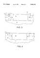
- FIG. 5is a top down schematic of the present invention.
- FIG. 6is a cross-sectional schematic of an alternative final product in accordance with the present invention.
- a standard silicon on insulator (“SOI”) substrateis provided.
- the standard SOIis a single crystalline semiconductor having a substantially planar surface and includes an insulative layer 14 and a thin semi-conductive layer 16 in a first surface area on the planar surface and a bulk area 12 in a second surface area of the planar surface.
- the bulk area 12is a single crystalline region having substantially the same crystalline structure as the planar surface.
- the insulative layer 14is typically a silicon oxide and the single crystalline semiconductor materials are usually silicon.
- the substratemay be manufactured in a number of different ways including: silicon implanted with oxide (“SIMOX”) in which the bulk wafer is high energy implanted with a large dose of oxygen; bond and etch back (“BE-SOI”) in which two bulk wafers have an oxide grown on a surface and a dopant profile is incorporated in one of the wafers to act as a marker layer, the two oxide surfaces are bonded together and then one of the wafers is etched back to the marker dopant layer; or a method known as "smart cut” in which one of the wafers is hydrogen implanted before the first wafer is bonded to the second wafer, the two are bonded together and then the excess silicon of one of the wafers is cracked off using the hydrogen in the silicon structure to cause the cracking in the proper level, or by any other suitable means of making SOI.
- SIMOXsilicon implanted with oxide
- BE-SOIbond and etch back
- two bulk wafershave an oxide grown on a surface and a dop
- a thin polish stop layer 18(see FIG. 2), typically in the range of from about 5 nm to about 10 nm, of silicon nitride is deposited on the thin layer of silicon.
- a sacrificial layerin this case an oxide layer 20, typically about 100 nm thick, is then deposited on the thin nitride layer 18, as shown in FIG. 2.
- the oxide layer 20serves to provide a buffer region for subsequently grown epitaxial (“epi”) silicon. The buffer region avoids epi overgrowth on the nitride layer, thus improving the crystal quality at the edges of the array block, as will be explained further hereinafter.
- openings 22are formed in the oxide layer by the usual methods, typically by photolithographically defining the area using a photoresist material and then etching the defined area. The materials are etched through the oxide 20, nitride 18, SOI and back oxide layers 14 and 16, stopping on the top of the bulk substrate 12. These openings will form the array blocks in a DRAM product or the like. Electrically insulating spacers, such as nitride, or electrically conducting spacers, such as polysilicon 24 may then be formed in chosen locations around portions of the perimeter of the semiconductor on insulator region.
- a conductive spacer 24it will serve to electrically connect the semiconductor 16 of the SOI region to the substrate, because the resistivity of the spacer is substantially lower than that of any of the semiconductor regions to which it makes contact.
- materials for conductive spacersinclude, but are not limited to, doped polysilicon; intrinsic polysilicon; copper; aluminum-copper; titanium; titanium silicide; nickel silicide; and cobalt silicide.
- the spacers 24are formed using known methods, by depositing a layer of the desired spacer material and then directionally etching the material back to form the spacers. If spacers 24 are desired on one side but not the other, a block mask may be used to protect the desired spacer and the other spacers are etched away.
- a P-type epi layer 30is then grown up from the substrate surface.
- the epi layer 30may be grown either selectively or non-selectively. If growth is non-selective, the silicon that grows on the surface of the pad oxide layer may be removed by polishing the entire surface. Non-selective growth may be chosen for the easily controllable reaction conditions and the time savings. Growth conditions are adjusted so that the top surface of the epi is at least as high as the upper surface of the thin polish stop 18.
- the substrate prior to polishingis shown in FIG. 3.
- polishing the epitaxially grown silicon regionsrequires the use of a polishing slurry that is selective to the oxide and the nitride polish stops.
- the polishing padis preferably rigid to avoid excessive recessing of the epi with respect to the polish stop surface.
- the polishing processwould involve two polishing steps. The first step will polish the epi using the oxide layer as the polish stop. This will typically recess the surface of the epi 30 below the oxide surface. If epi growth is controlled well enough to stop before the top of the oxide layer, this first step is unnecessary. After the first polish, the second epi polish will use the nitride as the polish stop.
- the same pad and slurrymay be used in the second step as was used for the first polish.
- This stepplanarizes the epi 30 to the top of the nitride 18.
- the polish timeswill be determined by the amount of epi growth. The closer the height of the epi 18 is to the height of the nitride stop 18, the less polishing is required.
- An ideal deposition target, accounting for uniformity and some overgrowth for defects,might be the midpoint of the oxide stop. Since the top surface of the epi should be within a few hundred angstroms of the top of the nitride layer, any dishing that may occur should be minor and not result in depth of focus concerns for the array area relative to the SOI area.
- an area 100 of SOIis completely surrounded by a bulk area 102, which is in turn completely surrounded by areas of SOI 104.
- First or conductive spacers 105are provided along two edges or a first portion of the perimeter of the interior SOI 100.
- a second or insulative spacer 107is provided along one edge or a second portion of the perimeter of the bulk area 102.
- the epitaxially grown siliconis directly in contact with the SOI region.
- the epimay be grown in the opening contacting all the adjacent SOI regions. This provides a body contact to the SOI regions adjacent the opening. This would be used with critical circuitry that would suffer from floating body effects such as passgate metal oxide semiconductor field effect transistors (MOSFET's) or devices requiring close matching such as sense amplifiers or static random access memory (SRAM) cells.
- MOSFET'spassgate metal oxide semiconductor field effect transistors
- SRAMstatic random access memory
- Insulative spacers on all sides of the SOIallow non-contacted body SOI devices to be constructed adjacent the bulk devices. This provides the maximum performance advantages of SOI when the detrimental floating body effects are not severe enough to result in a loss of device stability, i.e., with grounded source devices that operate with low voltage power supplies, typically less than 1.5 V.
- Insulative spacersmay be used on one edge of the SOI without spacers on any of the other edges. This arrangement provides layout flexibility for forming combinations of contacted body SOI, bulk, and floating body SOI devices near each other.
- Conductive spacersmay be provided on all sides of the SOI region. This arrangement provides very low electrical resistance and thermal paths from the body of the SOI to the substrate. This is useful for providing stability for higher voltage applications where body current may be relatively large. This also provides improved power dissipation capability for SOI as compared to the arrangement in which the epi is grown contacting the SOI regions.
- a conductive spacer 124is formed to first provide the very low resistance path from SOI region 120 to the substrate, and an insulative spacer 126 is formed on the conductive spacer 124 to provide dielectric isolation between the SOI region 120 and the adjacent bulk device region 122.
- the insulative spacer 126may also be created in the same step in selected portions of the perimeter where the conductive spacer 124 is not present, and may not be in selected portions of the perimeter where the conductive spacer 124 is present, depending on the desired structure and function of the various parametrial devices.
- the ability to include portions that are both electrically contacted to the substrate while being dielectrically isolated from the epi regionis useful and important for low-noise and mixed analog/digital applications.
Landscapes
- Engineering & Computer Science (AREA)
- Physics & Mathematics (AREA)
- Condensed Matter Physics & Semiconductors (AREA)
- General Physics & Mathematics (AREA)
- Manufacturing & Machinery (AREA)
- Computer Hardware Design (AREA)
- Microelectronics & Electronic Packaging (AREA)
- Power Engineering (AREA)
- Element Separation (AREA)
- Recrystallisation Techniques (AREA)
- Semiconductor Memories (AREA)
- Thin Film Transistor (AREA)
Abstract
Description
Claims (19)
Priority Applications (7)
| Application Number | Priority Date | Filing Date | Title |
|---|---|---|---|
| US08/878,225US5894152A (en) | 1997-06-18 | 1997-06-18 | SOI/bulk hybrid substrate and method of forming the same |
| TW087106112ATW405220B (en) | 1997-06-18 | 1998-04-21 | Soi/bulk hybrid substrate and method of forming the same |
| KR1019980017441AKR100289830B1 (en) | 1997-06-18 | 1998-05-14 | Soi/bulk hybrid substrate and method of forming the same |
| MYPI98002182AMY117502A (en) | 1997-06-18 | 1998-05-15 | Soi/bulk hybrid substrate and method of forming the same. |
| CN98108451ACN1123071C (en) | 1997-06-18 | 1998-05-15 | SOI/bulk hybrid substrate and method of forming the same |
| JP10160221AJP2980586B2 (en) | 1997-06-18 | 1998-06-09 | Semiconductor device and manufacturing method thereof |
| US09/187,292US6107125A (en) | 1997-06-18 | 1998-11-05 | SOI/bulk hybrid substrate and method of forming the same |
Applications Claiming Priority (1)
| Application Number | Priority Date | Filing Date | Title |
|---|---|---|---|
| US08/878,225US5894152A (en) | 1997-06-18 | 1997-06-18 | SOI/bulk hybrid substrate and method of forming the same |
Related Child Applications (1)
| Application Number | Title | Priority Date | Filing Date |
|---|---|---|---|
| US09/187,292DivisionUS6107125A (en) | 1997-06-18 | 1998-11-05 | SOI/bulk hybrid substrate and method of forming the same |
Publications (1)
| Publication Number | Publication Date |
|---|---|
| US5894152Atrue US5894152A (en) | 1999-04-13 |
Family
ID=25371618
Family Applications (2)
| Application Number | Title | Priority Date | Filing Date |
|---|---|---|---|
| US08/878,225Expired - LifetimeUS5894152A (en) | 1997-06-18 | 1997-06-18 | SOI/bulk hybrid substrate and method of forming the same |
| US09/187,292Expired - LifetimeUS6107125A (en) | 1997-06-18 | 1998-11-05 | SOI/bulk hybrid substrate and method of forming the same |
Family Applications After (1)
| Application Number | Title | Priority Date | Filing Date |
|---|---|---|---|
| US09/187,292Expired - LifetimeUS6107125A (en) | 1997-06-18 | 1998-11-05 | SOI/bulk hybrid substrate and method of forming the same |
Country Status (6)
| Country | Link |
|---|---|
| US (2) | US5894152A (en) |
| JP (1) | JP2980586B2 (en) |
| KR (1) | KR100289830B1 (en) |
| CN (1) | CN1123071C (en) |
| MY (1) | MY117502A (en) |
| TW (1) | TW405220B (en) |
Cited By (43)
| Publication number | Priority date | Publication date | Assignee | Title |
|---|---|---|---|---|
| US6114197A (en)* | 1998-02-26 | 2000-09-05 | Sharp Laboratories Of America, Inc. | Method of forming fully depleted SIMOX CMOS having electrostatic discharge protection |
| US6201761B1 (en) | 2000-01-26 | 2001-03-13 | Advanced Micro Devices, Inc. | Field effect transistor with controlled body bias |
| US6229187B1 (en) | 1999-10-20 | 2001-05-08 | Advanced Micro Devices, Inc. | Field effect transistor with non-floating body and method for forming same on a bulk silicon wafer |
| US6245636B1 (en) | 1999-10-20 | 2001-06-12 | Advanced Micro Devices, Inc. | Method of formation of pseudo-SOI structures with direct contact of transistor body to the substrate |
| US6255147B1 (en) | 2000-01-31 | 2001-07-03 | Advanced Micro Devices, Inc. | Silicon on insulator circuit structure with extra narrow field transistors and method of forming same |
| US6261876B1 (en) | 1999-11-04 | 2001-07-17 | International Business Machines Corporation | Planar mixed SOI-bulk substrate for microelectronic applications |
| US6313507B1 (en) | 1998-12-24 | 2001-11-06 | Hyundai Electronics Industries Co., Ltd. | SOI semiconductor device capable of preventing floating body effect |
| US6350653B1 (en) | 2000-10-12 | 2002-02-26 | International Business Machines Corporation | Embedded DRAM on silicon-on-insulator substrate |
| US6376286B1 (en)* | 1999-10-20 | 2002-04-23 | Advanced Micro Devices, Inc. | Field effect transistor with non-floating body and method for forming same on a bulk silicon wafer |
| US6404014B1 (en)* | 1999-02-16 | 2002-06-11 | International Business Machines Corporation | Planar and densely patterned silicon-on-insulator structure |
| US6429070B1 (en) | 2000-08-30 | 2002-08-06 | Micron Technology, Inc. | DRAM cell constructions, and methods of forming DRAM cells |
| US6465852B1 (en) | 1999-10-20 | 2002-10-15 | Advanced Micro Devices, Inc. | Silicon wafer including both bulk and SOI regions and method for forming same on a bulk silicon wafer |
| US6498372B2 (en)* | 2001-02-16 | 2002-12-24 | International Business Machines Corporation | Conductive coupling of electrical structures to a semiconductor device located under a buried oxide layer |
| US6501134B1 (en)* | 2001-01-09 | 2002-12-31 | Advanced Micro Devices, Inc. | Ultra thin SOI devices with improved short-channel control |
| US6514809B1 (en)* | 2000-11-03 | 2003-02-04 | Advanced Micro Devices, Inc. | SOI field effect transistors with body contacts formed by selective etch and fill |
| US20030057490A1 (en)* | 2001-09-26 | 2003-03-27 | Kabushiki Kaisha Toshiba | Semiconductor device substrate and method of manufacturing semiconductor device substrate |
| US20030057487A1 (en)* | 2001-09-27 | 2003-03-27 | Kabushiki Kaisha Toshiba | Semiconductor chip having multiple functional blocks integrated in a single chip and method for fabricating the same |
| US6544837B1 (en) | 2000-03-17 | 2003-04-08 | International Business Machines Corporation | SOI stacked DRAM logic |
| US6630714B2 (en)* | 2001-12-27 | 2003-10-07 | Kabushiki Kaisha Toshiba | Semiconductor device formed in semiconductor layer arranged on substrate with one of insulating film and cavity interposed between the substrate and the semiconductor layer |
| US6635552B1 (en) | 2000-06-12 | 2003-10-21 | Micron Technology, Inc. | Methods of forming semiconductor constructions |
| US20040041265A1 (en)* | 2002-08-29 | 2004-03-04 | Micron Technology, Inc. | Localized biasing for silicon on insulator structures |
| US20040040492A1 (en)* | 2002-09-04 | 2004-03-04 | Kiyofumi Sakaguchi | Substrate and manufacturing method therefor |
| US20040048454A1 (en)* | 2002-09-10 | 2004-03-11 | Kiyofumi Sakaguchi | Substrate and manufacturing method therefor |
| US20040048091A1 (en)* | 2002-09-11 | 2004-03-11 | Nobuhiko Sato | Substrate and manufacturing method therefor |
| US20040058511A1 (en)* | 2002-09-04 | 2004-03-25 | Kiyofumi Sakaguchi | Substrate and manufacturing method therefor |
| US20040150044A1 (en)* | 2003-01-21 | 2004-08-05 | Hajime Nagano | Element formation substrate, method of manufacturing the same, and semiconductor device |
| US6777288B1 (en)* | 2002-11-06 | 2004-08-17 | National Semiconductor Corporation | Vertical MOS transistor |
| US20040164334A1 (en)* | 2000-06-09 | 2004-08-26 | Masleid Robert P. | Hybrid bulk/silicon-on-insulator multiprocessors |
| US6828202B1 (en) | 2002-10-01 | 2004-12-07 | T-Ram, Inc. | Semiconductor region self-aligned with ion implant shadowing |
| US20040248363A1 (en)* | 2003-06-09 | 2004-12-09 | International Business Machines Corporation | Soi trench capacitor cell incorporating a low-leakage floating body array transistor |
| US6855976B2 (en)* | 2001-12-27 | 2005-02-15 | Kabushiki Kaisha Toshiba | Semiconductor device using partial SOI substrate and manufacturing method thereof |
| US20050282392A1 (en)* | 2004-06-16 | 2005-12-22 | International Business Machines Corporation | Sti formation in semiconductor device including soi and bulk silicon regions |
| US20060065954A1 (en)* | 2004-03-12 | 2006-03-30 | Nowak Edward J | High-performance CMOS SOI devices on hybrid crystal-oriented substrates |
| US20060091427A1 (en)* | 2004-11-01 | 2006-05-04 | Advanced Micro Devices, Inc. | Silicon-on-insulator semiconductor device with silicon layers having different crystal orientations and method of forming the silicon-on-insulator semiconductor device |
| US20070228377A1 (en)* | 2006-03-31 | 2007-10-04 | Karsten Wieczorek | Semiconductor device comprising soi transistors and bulk transistors and a method of forming the same |
| US20090032874A1 (en)* | 2007-07-05 | 2009-02-05 | Stmicroelectronics Sa | Method for integrating silicon-on-nothing devices with standard cmos devices |
| EP1875507A4 (en)* | 2005-04-15 | 2009-08-05 | Ibm | HYBRID CRYSTALLINE ORIENTATION CMOS STRUCTURE FOR ADAPTIVE WELL POLARIZATION AND IMPROVING POWER AND PERFORMANCE |
| US20090256202A1 (en)* | 2008-04-14 | 2009-10-15 | Abou-Khalil Michel J | Semiconductor-on-insulator device structures with a body-to-substrate connection for enhanced electrostatic discharge protection, and design structures for such semiconductor-on-insulator device structures |
| US20090302387A1 (en)* | 2006-04-07 | 2009-12-10 | International Business Machines Corporation | Integrated circuit chip with fets having mixed body thicknesses and method of manufacture thereof |
| US8877609B2 (en) | 2011-05-11 | 2014-11-04 | Shin-Etsu Handotai Co., Ltd. | Method for manufacturing bonded substrate having an insulator layer in part of bonded substrate |
| US8912055B2 (en) | 2011-05-03 | 2014-12-16 | Imec | Method for manufacturing a hybrid MOSFET device and hybrid MOSFET obtainable thereby |
| US8916426B2 (en) | 2012-03-27 | 2014-12-23 | International Business Machines Corporation | Passive devices for FinFET integrated circuit technologies |
| US9059041B2 (en) | 2013-07-02 | 2015-06-16 | International Business Machines Corporation | Dual channel hybrid semiconductor-on-insulator semiconductor devices |
Families Citing this family (41)
| Publication number | Priority date | Publication date | Assignee | Title |
|---|---|---|---|---|
| US6245600B1 (en)* | 1999-07-01 | 2001-06-12 | International Business Machines Corporation | Method and structure for SOI wafers to avoid electrostatic discharge |
| TW469596B (en)* | 2000-04-19 | 2001-12-21 | Winbond Electronics Corp | Structure of SOI having substrate contact |
| KR100374554B1 (en)* | 2000-09-22 | 2003-03-04 | 주식회사 하이닉스반도체 | Structure of body-substrate contact for soi semiconductor device and method for fabricating the same |
| US6462381B1 (en)* | 2001-02-22 | 2002-10-08 | Advanced Micro Devices, Inc. | Silicon-on-insulator (SOI) electrostatic discharge (ESD) protection device with backside contact opening |
| JP2003100861A (en)* | 2001-09-20 | 2003-04-04 | Mitsubishi Electric Corp | Method for manufacturing semiconductor device |
| JP2007180569A (en)* | 2001-12-27 | 2007-07-12 | Toshiba Corp | Semiconductor device |
| JP2003203967A (en) | 2001-12-28 | 2003-07-18 | Toshiba Corp | Method for manufacturing partial SOI wafer, semiconductor device, and method for manufacturing the same |
| JP3974542B2 (en) | 2003-03-17 | 2007-09-12 | 株式会社東芝 | Semiconductor substrate manufacturing method and semiconductor device manufacturing method |
| US6867433B2 (en)* | 2003-04-30 | 2005-03-15 | Taiwan Semiconductor Manufacturing Company, Ltd. | Semiconductor-on-insulator chip incorporating strained-channel partially-depleted, fully-depleted, and multiple-gate transistors |
| US6936910B2 (en)* | 2003-05-09 | 2005-08-30 | International Business Machines Corporation | BiCMOS technology on SOI substrates |
| US20040222436A1 (en)* | 2003-05-09 | 2004-11-11 | International Business Machines Corporation | Bicmos technology on soi substrates |
| US20050012087A1 (en)* | 2003-07-15 | 2005-01-20 | Yi-Ming Sheu | Self-aligned MOSFET having an oxide region below the channel |
| US6936881B2 (en)* | 2003-07-25 | 2005-08-30 | Taiwan Semiconductor Manufacturing Company, Ltd. | Capacitor that includes high permittivity capacitor dielectric |
| US6940705B2 (en)* | 2003-07-25 | 2005-09-06 | Taiwan Semiconductor Manufacturing Company, Ltd. | Capacitor with enhanced performance and method of manufacture |
| US7078742B2 (en)* | 2003-07-25 | 2006-07-18 | Taiwan Semiconductor Manufacturing Co., Ltd. | Strained-channel semiconductor structure and method of fabricating the same |
| US7101742B2 (en)* | 2003-08-12 | 2006-09-05 | Taiwan Semiconductor Manufacturing Company, Ltd. | Strained channel complementary field-effect transistors and methods of manufacture |
| US20050035369A1 (en)* | 2003-08-15 | 2005-02-17 | Chun-Chieh Lin | Structure and method of forming integrated circuits utilizing strained channel transistors |
| US7112495B2 (en)* | 2003-08-15 | 2006-09-26 | Taiwan Semiconductor Manufacturing Company, Ltd. | Structure and method of a strained channel transistor and a second semiconductor component in an integrated circuit |
| US20050035410A1 (en)* | 2003-08-15 | 2005-02-17 | Yee-Chia Yeo | Semiconductor diode with reduced leakage |
| US7071052B2 (en)* | 2003-08-18 | 2006-07-04 | Taiwan Semiconductor Manufacturing Company, Ltd. | Resistor with reduced leakage |
| JP2005072084A (en) | 2003-08-28 | 2005-03-17 | Toshiba Corp | Semiconductor device and manufacturing method thereof |
| US7888201B2 (en) | 2003-11-04 | 2011-02-15 | Taiwan Semiconductor Manufacturing Company, Ltd. | Semiconductor-on-insulator SRAM configured using partially-depleted and fully-depleted transistors |
| US7087965B2 (en) | 2004-04-22 | 2006-08-08 | International Business Machines Corporation | Strained silicon CMOS on hybrid crystal orientations |
| US7208815B2 (en)* | 2004-05-28 | 2007-04-24 | Taiwan Semiconductor Manufacturing Company, Ltd. | CMOS logic gate fabricated on hybrid crystal orientations and method of forming thereof |
| US7112455B2 (en) | 2004-06-10 | 2006-09-26 | Freescale Semiconductor, Inc | Semiconductor optical devices and method for forming |
| DE102004032917B4 (en)* | 2004-07-07 | 2010-01-28 | Qimonda Ag | Method for producing a double-gate transistor |
| US7422956B2 (en)* | 2004-12-08 | 2008-09-09 | Advanced Micro Devices, Inc. | Semiconductor device and method of making semiconductor device comprising multiple stacked hybrid orientation layers |
| US7223640B2 (en)* | 2005-03-03 | 2007-05-29 | Advanced Micro Devices, Inc. | Semiconductor component and method of manufacture |
| WO2006103491A1 (en)* | 2005-03-29 | 2006-10-05 | S.O.I.Tec Silicon On Insulator Technologies | Hybrid fully soi-type multilayer structure |
| KR100688546B1 (en)* | 2005-05-13 | 2007-03-02 | 삼성전자주식회사 | Semiconductor device with decoupling capacitor and manufacturing method thereof |
| US7432149B2 (en)* | 2005-06-23 | 2008-10-07 | Taiwan Semiconductor Manufacturing Company, Ltd. | CMOS on SOI substrates with hybrid crystal orientations |
| US7611937B2 (en)* | 2005-06-24 | 2009-11-03 | Taiwan Semiconductor Manufacturing Company, Ltd. | High performance transistors with hybrid crystal orientations |
| US7531392B2 (en) | 2006-02-27 | 2009-05-12 | International Business Machines Corporation | Multi-orientation semiconductor-on-insulator (SOI) substrate, and method of fabricating same |
| US7396407B2 (en)* | 2006-04-18 | 2008-07-08 | International Business Machines Corporation | Trench-edge-defect-free recrystallization by edge-angle-optimized solid phase epitaxy: method and applications to hybrid orientation substrates |
| US7820501B2 (en) | 2006-10-11 | 2010-10-26 | International Business Machines Corporation | Decoder for a stationary switch machine |
| JP2008172082A (en)* | 2007-01-12 | 2008-07-24 | Toshiba Corp | Semiconductor device and manufacturing method of semiconductor device |
| US8558278B2 (en) | 2007-01-16 | 2013-10-15 | Taiwan Semiconductor Manufacturing Company, Ltd. | Strained transistor with optimized drive current and method of forming |
| US7393738B1 (en)* | 2007-01-16 | 2008-07-01 | International Business Machines Corporation | Subground rule STI fill for hot structure |
| US7772048B2 (en)* | 2007-02-23 | 2010-08-10 | Freescale Semiconductor, Inc. | Forming semiconductor fins using a sacrificial fin |
| US7943961B2 (en) | 2008-03-13 | 2011-05-17 | Taiwan Semiconductor Manufacturing Company, Ltd. | Strain bars in stressed layers of MOS devices |
| US7808051B2 (en) | 2008-09-29 | 2010-10-05 | Taiwan Semiconductor Manufacturing Company, Ltd. | Standard cell without OD space effect in Y-direction |
Citations (11)
| Publication number | Priority date | Publication date | Assignee | Title |
|---|---|---|---|---|
| US3943555A (en)* | 1974-05-02 | 1976-03-09 | Rca Corporation | SOS Bipolar transistor |
| US5032529A (en)* | 1988-08-24 | 1991-07-16 | Harris Corporation | Trench gate VCMOS method of manufacture |
| EP0610599A1 (en)* | 1993-01-04 | 1994-08-17 | Texas Instruments Incorporated | High voltage transistor with drift region |
| US5399507A (en)* | 1994-06-27 | 1995-03-21 | Motorola, Inc. | Fabrication of mixed thin-film and bulk semiconductor substrate for integrated circuit applications |
| US5484738A (en)* | 1992-06-17 | 1996-01-16 | International Business Machines Corporation | Method of forming silicon on oxide semiconductor device structure for BiCMOS integrated circuits |
| US5548149A (en)* | 1993-06-24 | 1996-08-20 | Texas Instruments Incorporated | Varying the thickness of the surface silicon layer in a silicon-on-insulator substrate |
| US5554870A (en)* | 1994-02-04 | 1996-09-10 | Motorola, Inc. | Integrated circuit having both vertical and horizontal devices and process for making the same |
| US5581101A (en)* | 1995-01-03 | 1996-12-03 | International Business Machines Corporation | FET and/or bipolar devices formed in thin vertical silicon on insulator (SOI) structures |
| US5583358A (en)* | 1988-01-08 | 1996-12-10 | Hitachi, Ltd. | Semiconductor memory device having stacked capacitors |
| US5589695A (en)* | 1993-11-29 | 1996-12-31 | Texas Instruments Incorporated | High-performance high-voltage device structures |
| US5818069A (en)* | 1997-06-20 | 1998-10-06 | Advanced Micro Devices, Inc. | Ultra high density series-connected transistors formed on separate elevational levels |
Family Cites Families (3)
| Publication number | Priority date | Publication date | Assignee | Title |
|---|---|---|---|---|
| JPS6358817A (en)* | 1986-08-29 | 1988-03-14 | Toshiba Corp | Composite semiconductor crystal structure |
| JPS6412543A (en)* | 1987-07-07 | 1989-01-17 | Toshiba Corp | Manufacture of semiconductor device |
| US5273915A (en)* | 1992-10-05 | 1993-12-28 | Motorola, Inc. | Method for fabricating bipolar junction and MOS transistors on SOI |
- 1997
- 1997-06-18USUS08/878,225patent/US5894152A/ennot_activeExpired - Lifetime
- 1998
- 1998-04-21TWTW087106112Apatent/TW405220B/ennot_activeIP Right Cessation
- 1998-05-14KRKR1019980017441Apatent/KR100289830B1/ennot_activeExpired - Fee Related
- 1998-05-15CNCN98108451Apatent/CN1123071C/ennot_activeExpired - Lifetime
- 1998-05-15MYMYPI98002182Apatent/MY117502A/enunknown
- 1998-06-09JPJP10160221Apatent/JP2980586B2/ennot_activeExpired - Fee Related
- 1998-11-05USUS09/187,292patent/US6107125A/ennot_activeExpired - Lifetime
Patent Citations (12)
| Publication number | Priority date | Publication date | Assignee | Title |
|---|---|---|---|---|
| US3943555A (en)* | 1974-05-02 | 1976-03-09 | Rca Corporation | SOS Bipolar transistor |
| US5583358A (en)* | 1988-01-08 | 1996-12-10 | Hitachi, Ltd. | Semiconductor memory device having stacked capacitors |
| US5032529A (en)* | 1988-08-24 | 1991-07-16 | Harris Corporation | Trench gate VCMOS method of manufacture |
| US5484738A (en)* | 1992-06-17 | 1996-01-16 | International Business Machines Corporation | Method of forming silicon on oxide semiconductor device structure for BiCMOS integrated circuits |
| EP0610599A1 (en)* | 1993-01-04 | 1994-08-17 | Texas Instruments Incorporated | High voltage transistor with drift region |
| US5554546A (en)* | 1993-01-04 | 1996-09-10 | Texas Instruments Inc. | Method of fabricating a high voltage transistor |
| US5548149A (en)* | 1993-06-24 | 1996-08-20 | Texas Instruments Incorporated | Varying the thickness of the surface silicon layer in a silicon-on-insulator substrate |
| US5589695A (en)* | 1993-11-29 | 1996-12-31 | Texas Instruments Incorporated | High-performance high-voltage device structures |
| US5554870A (en)* | 1994-02-04 | 1996-09-10 | Motorola, Inc. | Integrated circuit having both vertical and horizontal devices and process for making the same |
| US5399507A (en)* | 1994-06-27 | 1995-03-21 | Motorola, Inc. | Fabrication of mixed thin-film and bulk semiconductor substrate for integrated circuit applications |
| US5581101A (en)* | 1995-01-03 | 1996-12-03 | International Business Machines Corporation | FET and/or bipolar devices formed in thin vertical silicon on insulator (SOI) structures |
| US5818069A (en)* | 1997-06-20 | 1998-10-06 | Advanced Micro Devices, Inc. | Ultra high density series-connected transistors formed on separate elevational levels |
Non-Patent Citations (5)
| Title |
|---|
| IBM/Selective SOI and Integration with Planar Oxide Isolated Bulk Devices/vol. 35 No. 5 Oct. 1992.* |
| IBM/Selective SOI and Integration with Planar Oxide-Isolated Bulk Devices/vol. 35 No. 5 Oct. 1992. |
| Proceedings 1996 IEEEE International SOI Conference, Oct. 1996/Floating Body Concerns for SOI Dynamic Random Access Memory.* |
| Proceedings 1996 IEEEE International SOI Conference, Oct. 1996/Floating-Body Concerns for SOI Dynamic Random Access Memory. |
| SOI/Bulk Hybrid Technology on Simox Wafers for High Performance Circuits with Good ESD Immunity/Manuscript/1995.* |
Cited By (98)
| Publication number | Priority date | Publication date | Assignee | Title |
|---|---|---|---|---|
| US6114197A (en)* | 1998-02-26 | 2000-09-05 | Sharp Laboratories Of America, Inc. | Method of forming fully depleted SIMOX CMOS having electrostatic discharge protection |
| US6313507B1 (en) | 1998-12-24 | 2001-11-06 | Hyundai Electronics Industries Co., Ltd. | SOI semiconductor device capable of preventing floating body effect |
| US6455396B1 (en) | 1998-12-24 | 2002-09-24 | Hyundai Electronics Industries Co., Ltd. | SOI semiconductor device capable of preventing floating body effect |
| US6404014B1 (en)* | 1999-02-16 | 2002-06-11 | International Business Machines Corporation | Planar and densely patterned silicon-on-insulator structure |
| US6245636B1 (en) | 1999-10-20 | 2001-06-12 | Advanced Micro Devices, Inc. | Method of formation of pseudo-SOI structures with direct contact of transistor body to the substrate |
| US6376286B1 (en)* | 1999-10-20 | 2002-04-23 | Advanced Micro Devices, Inc. | Field effect transistor with non-floating body and method for forming same on a bulk silicon wafer |
| US6229187B1 (en) | 1999-10-20 | 2001-05-08 | Advanced Micro Devices, Inc. | Field effect transistor with non-floating body and method for forming same on a bulk silicon wafer |
| US6465852B1 (en) | 1999-10-20 | 2002-10-15 | Advanced Micro Devices, Inc. | Silicon wafer including both bulk and SOI regions and method for forming same on a bulk silicon wafer |
| US6261876B1 (en) | 1999-11-04 | 2001-07-17 | International Business Machines Corporation | Planar mixed SOI-bulk substrate for microelectronic applications |
| US6201761B1 (en) | 2000-01-26 | 2001-03-13 | Advanced Micro Devices, Inc. | Field effect transistor with controlled body bias |
| US6255147B1 (en) | 2000-01-31 | 2001-07-03 | Advanced Micro Devices, Inc. | Silicon on insulator circuit structure with extra narrow field transistors and method of forming same |
| US6544837B1 (en) | 2000-03-17 | 2003-04-08 | International Business Machines Corporation | SOI stacked DRAM logic |
| US6590258B2 (en) | 2000-03-17 | 2003-07-08 | International Business Machines Corporation | SIO stacked DRAM logic |
| US20040164334A1 (en)* | 2000-06-09 | 2004-08-26 | Masleid Robert P. | Hybrid bulk/silicon-on-insulator multiprocessors |
| US6864524B2 (en)* | 2000-06-09 | 2005-03-08 | Fujitsu Limited | Hybrid bulk/silicon-on-insulator multiprocessors |
| US7045439B2 (en) | 2000-06-12 | 2006-05-16 | Micron Technology, Inc. | Methods of forming semiconductor constructions |
| US6638834B2 (en) | 2000-06-12 | 2003-10-28 | Micron Technology, Inc. | Methods of forming semiconductor constructions |
| US6844243B1 (en) | 2000-06-12 | 2005-01-18 | Micron Technology, Inc. | Methods of forming semiconductor constructions |
| US6653677B2 (en) | 2000-06-12 | 2003-11-25 | Micron Technology, Inc. | Semiconductor constructions |
| US6635552B1 (en) | 2000-06-12 | 2003-10-21 | Micron Technology, Inc. | Methods of forming semiconductor constructions |
| US6734062B2 (en) | 2000-08-30 | 2004-05-11 | Micron Technology, Inc. | Methods of forming DRAM cells |
| US6707090B2 (en) | 2000-08-30 | 2004-03-16 | Micron Technology, Inc. | DRAM cell constructions |
| US6429070B1 (en) | 2000-08-30 | 2002-08-06 | Micron Technology, Inc. | DRAM cell constructions, and methods of forming DRAM cells |
| US20030160242A1 (en)* | 2000-08-30 | 2003-08-28 | Fernando Gonzalez | DRAM cell constructions |
| US6639243B2 (en) | 2000-08-30 | 2003-10-28 | Micron Technology, Inc. | DRAM cell constructions |
| US6590259B2 (en)* | 2000-10-12 | 2003-07-08 | International Business Machines Corporation | Semiconductor device of an embedded DRAM on SOI substrate |
| US6350653B1 (en) | 2000-10-12 | 2002-02-26 | International Business Machines Corporation | Embedded DRAM on silicon-on-insulator substrate |
| SG108827A1 (en)* | 2000-10-12 | 2005-02-28 | Ibm | Embedded dram on silicon-on-insulator substrate |
| US6514809B1 (en)* | 2000-11-03 | 2003-02-04 | Advanced Micro Devices, Inc. | SOI field effect transistors with body contacts formed by selective etch and fill |
| US6501134B1 (en)* | 2001-01-09 | 2002-12-31 | Advanced Micro Devices, Inc. | Ultra thin SOI devices with improved short-channel control |
| US6498372B2 (en)* | 2001-02-16 | 2002-12-24 | International Business Machines Corporation | Conductive coupling of electrical structures to a semiconductor device located under a buried oxide layer |
| US7521300B2 (en) | 2001-09-26 | 2009-04-21 | Kabushiki Kaisha Toshiba | Semiconductor device substrate including a single-crystalline layer and method of manufacturing semiconductor device substrate |
| US20060234478A1 (en)* | 2001-09-26 | 2006-10-19 | Kabushiki Kaisha Toshiba | Semiconductor device substrate and method of manufacturing semiconductor device substrate |
| US7187035B2 (en) | 2001-09-26 | 2007-03-06 | Kabushiki Kaisha Toshiba | Semiconductor device comprising multiple layers with trenches formed on a semiconductor substrate |
| US20030057490A1 (en)* | 2001-09-26 | 2003-03-27 | Kabushiki Kaisha Toshiba | Semiconductor device substrate and method of manufacturing semiconductor device substrate |
| US7018904B2 (en) | 2001-09-27 | 2006-03-28 | Kabushiki Kaisha Toshiba | Semiconductor chip having multiple functional blocks integrated in a single chip and method for fabricating the same |
| US6835981B2 (en) | 2001-09-27 | 2004-12-28 | Kabushiki Kaisha Toshiba | Semiconductor chip which combines bulk and SOI regions and separates same with plural isolation regions |
| US7148543B2 (en) | 2001-09-27 | 2006-12-12 | Kabushiki Kaisha Toshiba | Semiconductor chip which combines bulk and SOI regions and separates same with plural isolation regions |
| US20050019999A1 (en)* | 2001-09-27 | 2005-01-27 | Kabushiki Kaisha Toshiba | Semiconductor chip having multiple functional blocks integrated in a single chip and method for fabricating the same |
| US20030057487A1 (en)* | 2001-09-27 | 2003-03-27 | Kabushiki Kaisha Toshiba | Semiconductor chip having multiple functional blocks integrated in a single chip and method for fabricating the same |
| US20050156245A1 (en)* | 2001-12-27 | 2005-07-21 | Tsutomu Sato | Semiconductor device formed in semiconductor layer arranged on substrate with one of insulating film and cavity interposed between the substrate and the semiconductor layer |
| US6630714B2 (en)* | 2001-12-27 | 2003-10-07 | Kabushiki Kaisha Toshiba | Semiconductor device formed in semiconductor layer arranged on substrate with one of insulating film and cavity interposed between the substrate and the semiconductor layer |
| US20040026739A1 (en)* | 2001-12-27 | 2004-02-12 | Tsutomu Sato | Semiconductor device formed in semiconductor layer arranged on substrate with one of insulating film and cavity interposed between the substrate and the semiconductor layer |
| US7112822B2 (en) | 2001-12-27 | 2006-09-26 | Kabushiki Kaisha Toshiba | Semiconductor device using partial SOI substrate and manufacturing method thereof |
| US6855976B2 (en)* | 2001-12-27 | 2005-02-15 | Kabushiki Kaisha Toshiba | Semiconductor device using partial SOI substrate and manufacturing method thereof |
| US20080012078A1 (en)* | 2001-12-27 | 2008-01-17 | Tsutomu Sato | Semiconductor device formed in semiconductor layer arranged on substrate with one of insulating film and cavity interposed between the substrate and the semiconductor layer |
| US20060273330A1 (en)* | 2001-12-27 | 2006-12-07 | Hajime Nagano | Semiconductor device using partial SOI substrate and manufacturing method thereof |
| US20050093066A1 (en)* | 2001-12-27 | 2005-05-05 | Hajime Nagano | Semiconductor device using partial SOI substrate and manufacturing method thereof |
| US7420249B2 (en) | 2001-12-27 | 2008-09-02 | Kabushiki Kaisha Toshiba | Semiconductor device formed in semiconductor layer arranged on substrate with one of insulating film and cavity interposed between the substrate and the semiconductor layer |
| US7439112B2 (en) | 2001-12-27 | 2008-10-21 | Kabushiki Kaisha Toshiba | Semiconductor device using partial SOI substrate and manufacturing method thereof |
| US7019365B2 (en) | 2001-12-27 | 2006-03-28 | Kabushiki Kaisha Toshiba | Semiconductor device formed in semiconductor layer arranged on substrate with one of insulating film and cavity interposed between the substrate and the semiconductor layer |
| US7659152B2 (en) | 2002-08-29 | 2010-02-09 | Micron Technology, Inc. | Localized biasing for silicon on insulator structures |
| US7608927B2 (en) | 2002-08-29 | 2009-10-27 | Micron Technology, Inc. | Localized biasing for silicon on insulator structures |
| US20100012995A1 (en)* | 2002-08-29 | 2010-01-21 | Fernando Gonzalez | Localized biasing for silicon on insulator structures |
| US8159014B2 (en) | 2002-08-29 | 2012-04-17 | Micron Technology, Inc. | Localized biasing for silicon on insulator structures |
| US20050032284A1 (en)* | 2002-08-29 | 2005-02-10 | Micron Technology, Inc. | Localized biasing for silicon on insulator structures |
| US8643110B2 (en) | 2002-08-29 | 2014-02-04 | Micron Technology, Inc. | Localized biasing for silicon on insulator structures |
| US20040041265A1 (en)* | 2002-08-29 | 2004-03-04 | Micron Technology, Inc. | Localized biasing for silicon on insulator structures |
| US6951796B2 (en) | 2002-09-04 | 2005-10-04 | Canon Kabushiki Kaisha | Substrate and manufacturing method therefor |
| US20040058511A1 (en)* | 2002-09-04 | 2004-03-25 | Kiyofumi Sakaguchi | Substrate and manufacturing method therefor |
| US20040040492A1 (en)* | 2002-09-04 | 2004-03-04 | Kiyofumi Sakaguchi | Substrate and manufacturing method therefor |
| US6946354B2 (en) | 2002-09-10 | 2005-09-20 | Canon Kabushiki Kaisha | Substrate and manufacturing method therefor |
| US20040048454A1 (en)* | 2002-09-10 | 2004-03-11 | Kiyofumi Sakaguchi | Substrate and manufacturing method therefor |
| US20040048091A1 (en)* | 2002-09-11 | 2004-03-11 | Nobuhiko Sato | Substrate and manufacturing method therefor |
| US6828202B1 (en) | 2002-10-01 | 2004-12-07 | T-Ram, Inc. | Semiconductor region self-aligned with ion implant shadowing |
| US6777288B1 (en)* | 2002-11-06 | 2004-08-17 | National Semiconductor Corporation | Vertical MOS transistor |
| US6949421B1 (en) | 2002-11-06 | 2005-09-27 | National Semiconductor Corporation | Method of forming a vertical MOS transistor |
| US20080044983A1 (en)* | 2003-01-21 | 2008-02-21 | Kabushiki Kaisha Toshiba | Element formation substrate, method of manufacturing the same, and semiconductor device |
| US20040150044A1 (en)* | 2003-01-21 | 2004-08-05 | Hajime Nagano | Element formation substrate, method of manufacturing the same, and semiconductor device |
| US7285825B2 (en)* | 2003-01-21 | 2007-10-23 | Kabushiki Kaisha Toshiba | Element formation substrate for forming semiconductor device |
| US7510945B2 (en) | 2003-01-21 | 2009-03-31 | Kabushiki Kaisha Toshiba | Element formation substrate, method of manufacturing the same, and semiconductor device |
| US6964897B2 (en) | 2003-06-09 | 2005-11-15 | International Business Machines Corporation | SOI trench capacitor cell incorporating a low-leakage floating body array transistor |
| US20040248363A1 (en)* | 2003-06-09 | 2004-12-09 | International Business Machines Corporation | Soi trench capacitor cell incorporating a low-leakage floating body array transistor |
| US7498216B2 (en)* | 2004-03-12 | 2009-03-03 | International Business Machines Corporation | Method of forming high-performance CMOS SOI devices on hybrid crystal-oriented substrates |
| US20060065954A1 (en)* | 2004-03-12 | 2006-03-30 | Nowak Edward J | High-performance CMOS SOI devices on hybrid crystal-oriented substrates |
| US20060244093A1 (en)* | 2004-06-16 | 2006-11-02 | Steigerwalt Michael D | Sti formation in semiconductor device including soi and bulk silicon regions |
| US7118986B2 (en) | 2004-06-16 | 2006-10-10 | International Business Machines Corporation | STI formation in semiconductor device including SOI and bulk silicon regions |
| US20050282392A1 (en)* | 2004-06-16 | 2005-12-22 | International Business Machines Corporation | Sti formation in semiconductor device including soi and bulk silicon regions |
| US20060091427A1 (en)* | 2004-11-01 | 2006-05-04 | Advanced Micro Devices, Inc. | Silicon-on-insulator semiconductor device with silicon layers having different crystal orientations and method of forming the silicon-on-insulator semiconductor device |
| US7235433B2 (en)* | 2004-11-01 | 2007-06-26 | Advanced Micro Devices, Inc. | Silicon-on-insulator semiconductor device with silicon layers having different crystal orientations and method of forming the silicon-on-insulator semiconductor device |
| EP1875507A4 (en)* | 2005-04-15 | 2009-08-05 | Ibm | HYBRID CRYSTALLINE ORIENTATION CMOS STRUCTURE FOR ADAPTIVE WELL POLARIZATION AND IMPROVING POWER AND PERFORMANCE |
| US7629233B2 (en) | 2005-04-15 | 2009-12-08 | International Business Machines Corporation | Hybrid crystal orientation CMOS structure for adaptive well biasing and for power and performance enhancement |
| DE102006015076A1 (en)* | 2006-03-31 | 2007-10-11 | Advanced Micro Devices, Inc., Sunnyvale | Semiconductor device with SOI transistors and solid-state transistors and a method for manufacturing |
| US20070228377A1 (en)* | 2006-03-31 | 2007-10-04 | Karsten Wieczorek | Semiconductor device comprising soi transistors and bulk transistors and a method of forming the same |
| US7955937B2 (en) | 2006-03-31 | 2011-06-07 | Advanced Micro Devices, Inc. | Method for manufacturing semiconductor device comprising SOI transistors and bulk transistors |
| DE102006015076B4 (en)* | 2006-03-31 | 2014-03-20 | Advanced Micro Devices, Inc. | Semiconductor device with SOI transistors and solid-state transistors and a method for manufacturing |
| US20090302387A1 (en)* | 2006-04-07 | 2009-12-10 | International Business Machines Corporation | Integrated circuit chip with fets having mixed body thicknesses and method of manufacture thereof |
| US7968944B2 (en)* | 2006-04-07 | 2011-06-28 | International Business Machines Corporation | Integrated circuit chip with FETs having mixed body thicknesses and method of manufacture thereof |
| US20090032874A1 (en)* | 2007-07-05 | 2009-02-05 | Stmicroelectronics Sa | Method for integrating silicon-on-nothing devices with standard cmos devices |
| US7906381B2 (en) | 2007-07-05 | 2011-03-15 | Stmicroelectronics S.A. | Method for integrating silicon-on-nothing devices with standard CMOS devices |
| US8217455B2 (en)* | 2008-04-14 | 2012-07-10 | International Business Machines Corporation | Semiconductor-on-insulator device structures with a body-to-substrate connection for enhanced electrostatic discharge protection, and design structures for such semiconductor-on-insulator device structures |
| US20090256202A1 (en)* | 2008-04-14 | 2009-10-15 | Abou-Khalil Michel J | Semiconductor-on-insulator device structures with a body-to-substrate connection for enhanced electrostatic discharge protection, and design structures for such semiconductor-on-insulator device structures |
| US8912055B2 (en) | 2011-05-03 | 2014-12-16 | Imec | Method for manufacturing a hybrid MOSFET device and hybrid MOSFET obtainable thereby |
| US8877609B2 (en) | 2011-05-11 | 2014-11-04 | Shin-Etsu Handotai Co., Ltd. | Method for manufacturing bonded substrate having an insulator layer in part of bonded substrate |
| US8916426B2 (en) | 2012-03-27 | 2014-12-23 | International Business Machines Corporation | Passive devices for FinFET integrated circuit technologies |
| US9236398B2 (en) | 2012-03-27 | 2016-01-12 | Globalfoundries Inc. | Passive devices for FinFET integrated circuit technologies |
| US9059041B2 (en) | 2013-07-02 | 2015-06-16 | International Business Machines Corporation | Dual channel hybrid semiconductor-on-insulator semiconductor devices |
| US9293474B2 (en) | 2013-07-02 | 2016-03-22 | International Business Machines Corporation | Dual channel hybrid semiconductor-on-insulator semiconductor devices |
Also Published As
| Publication number | Publication date |
|---|---|
| JP2980586B2 (en) | 1999-11-22 |
| CN1202736A (en) | 1998-12-23 |
| TW405220B (en) | 2000-09-11 |
| KR19990006452A (en) | 1999-01-25 |
| MY117502A (en) | 2004-07-31 |
| US6107125A (en) | 2000-08-22 |
| KR100289830B1 (en) | 2001-12-12 |
| JPH1117001A (en) | 1999-01-22 |
| CN1123071C (en) | 2003-10-01 |
Similar Documents
| Publication | Publication Date | Title |
|---|---|---|
| US5894152A (en) | SOI/bulk hybrid substrate and method of forming the same | |
| JP3431734B2 (en) | SOI field effect transistor and method of manufacturing the same | |
| US6586284B2 (en) | Silicon-on-insulator (SOI) substrate, method for fabricating SOI substrate and SOI MOSFET using the SOI substrate | |
| JP4074451B2 (en) | Manufacturing method of semiconductor device | |
| US6133116A (en) | Methods of forming trench isolation regions having conductive shields therein | |
| JP3963970B2 (en) | DRAM cell and method of forming the same | |
| US7659152B2 (en) | Localized biasing for silicon on insulator structures | |
| US6268621B1 (en) | Vertical channel field effect transistor | |
| US20020115244A1 (en) | SOI MOSFET having body contact for preventing floating body effect and method of fabricating the same | |
| US6337253B1 (en) | Process of making buried capacitor for silicon-on-insulator structure | |
| US6294817B1 (en) | Source/drain-on insulator (S/DOI) field effect transistor using oxidized amorphous silicon and method of fabrication | |
| US7432560B2 (en) | Body-tied-to-source MOSFETs with asymmetrical source and drain regions and methods of fabricating the same | |
| US6633067B2 (en) | Compact SOI body contact link | |
| US20030025157A1 (en) | Deep trench body SOI contacts with epitaxial layer formation | |
| KR100486190B1 (en) | Memory cell for dynamic random access memory(dram) | |
| US6514809B1 (en) | SOI field effect transistors with body contacts formed by selective etch and fill | |
| US6300172B1 (en) | Method of field isolation in silicon-on-insulator technology | |
| US6420749B1 (en) | Trench field shield in trench isolation | |
| US7098102B2 (en) | Shallow trench isolation structure and dynamic random access memory, and fabricating methods thereof | |
| EP0905772A2 (en) | Trench capacitor DRAM cell and method of making the same | |
| WO2001043198A2 (en) | Source/drain-on-insulator (s/doi) field effect transistor using silicon nitride and silicon oxide and method of fabrication | |
| JPH0669450A (en) | Method of manufacturing SOI type dynamic semiconductor memory device | |
| HK1017500A (en) | Trench capacitor dram cell and method of making the same | |
| HK1017771A (en) | Trench capacitor dram cell and method of making the same |
Legal Events
| Date | Code | Title | Description |
|---|---|---|---|
| AS | Assignment | Owner name:INTERNATIONAL BUSINESS MACHINES CORPORATION, NEW Y Free format text:ASSIGNMENT OF ASSIGNORS INTEREST;ASSIGNORS:JASO, MARK A.;MANDELMAN, JACK A.;TONTI, WILLIAM R.;AND OTHERS;REEL/FRAME:008617/0607;SIGNING DATES FROM 19970530 TO 19970609 | |
| AS | Assignment | Owner name:INTERNATIONAL BUSINESS MACHINES CORPORATION, NEW Y Free format text:RE-RECORD TO CORRECT THE EXECUTION DATES OF THE CONVEYING PARTIES PREVIOUSLY RECORDED ON REEL 8617, FRAME 0607;ASSIGNORS:JASO, MARK A.;MANDELMAN, JACK A.;TONTI, WILLIAM R.;AND OTHERS;REEL/FRAME:008763/0327;SIGNING DATES FROM 19970530 TO 19970609 | |
| STCF | Information on status: patent grant | Free format text:PATENTED CASE | |
| FEPP | Fee payment procedure | Free format text:PAYOR NUMBER ASSIGNED (ORIGINAL EVENT CODE: ASPN); ENTITY STATUS OF PATENT OWNER: LARGE ENTITY | |
| FPAY | Fee payment | Year of fee payment:4 | |
| FPAY | Fee payment | Year of fee payment:8 | |
| FPAY | Fee payment | Year of fee payment:12 | |
| AS | Assignment | Owner name:GLOBALFOUNDRIES U.S. 2 LLC, NEW YORK Free format text:ASSIGNMENT OF ASSIGNORS INTEREST;ASSIGNOR:INTERNATIONAL BUSINESS MACHINES CORPORATION;REEL/FRAME:036550/0001 Effective date:20150629 | |
| AS | Assignment | Owner name:GLOBALFOUNDRIES INC., CAYMAN ISLANDS Free format text:ASSIGNMENT OF ASSIGNORS INTEREST;ASSIGNORS:GLOBALFOUNDRIES U.S. 2 LLC;GLOBALFOUNDRIES U.S. INC.;REEL/FRAME:036779/0001 Effective date:20150910 | |
| AS | Assignment | Owner name:GLOBALFOUNDRIES U.S. INC., NEW YORK Free format text:RELEASE BY SECURED PARTY;ASSIGNOR:WILMINGTON TRUST, NATIONAL ASSOCIATION;REEL/FRAME:056987/0001 Effective date:20201117 |