US5893756A - Use of ethylene glycol as a corrosion inhibitor during cleaning after metal chemical mechanical polishing - Google Patents
Use of ethylene glycol as a corrosion inhibitor during cleaning after metal chemical mechanical polishingDownload PDFInfo
- Publication number
- US5893756A US5893756AUS08/918,483US91848397AUS5893756AUS 5893756 AUS5893756 AUS 5893756AUS 91848397 AUS91848397 AUS 91848397AUS 5893756 AUS5893756 AUS 5893756A
- Authority
- US
- United States
- Prior art keywords
- amount
- substrate surface
- ethylene glycol
- hydrofluoric acid
- dielectric layer
- Prior art date
- Legal status (The legal status is an assumption and is not a legal conclusion. Google has not performed a legal analysis and makes no representation as to the accuracy of the status listed.)
- Expired - Lifetime
Links
Images


Classifications
- C—CHEMISTRY; METALLURGY
- C23—COATING METALLIC MATERIAL; COATING MATERIAL WITH METALLIC MATERIAL; CHEMICAL SURFACE TREATMENT; DIFFUSION TREATMENT OF METALLIC MATERIAL; COATING BY VACUUM EVAPORATION, BY SPUTTERING, BY ION IMPLANTATION OR BY CHEMICAL VAPOUR DEPOSITION, IN GENERAL; INHIBITING CORROSION OF METALLIC MATERIAL OR INCRUSTATION IN GENERAL
- C23F—NON-MECHANICAL REMOVAL OF METALLIC MATERIAL FROM SURFACE; INHIBITING CORROSION OF METALLIC MATERIAL OR INCRUSTATION IN GENERAL; MULTI-STEP PROCESSES FOR SURFACE TREATMENT OF METALLIC MATERIAL INVOLVING AT LEAST ONE PROCESS PROVIDED FOR IN CLASS C23 AND AT LEAST ONE PROCESS COVERED BY SUBCLASS C21D OR C22F OR CLASS C25
- C23F11/00—Inhibiting corrosion of metallic material by applying inhibitors to the surface in danger of corrosion or adding them to the corrosive agent
- C23F11/08—Inhibiting corrosion of metallic material by applying inhibitors to the surface in danger of corrosion or adding them to the corrosive agent in other liquids
- C23F11/10—Inhibiting corrosion of metallic material by applying inhibitors to the surface in danger of corrosion or adding them to the corrosive agent in other liquids using organic inhibitors
- C23F11/12—Oxygen-containing compounds
- C23F11/122—Alcohols; Aldehydes; Ketones
- H—ELECTRICITY
- H01—ELECTRIC ELEMENTS
- H01L—SEMICONDUCTOR DEVICES NOT COVERED BY CLASS H10
- H01L21/00—Processes or apparatus adapted for the manufacture or treatment of semiconductor or solid state devices or of parts thereof
- H01L21/02—Manufacture or treatment of semiconductor devices or of parts thereof
- H01L21/02041—Cleaning
- H01L21/02057—Cleaning during device manufacture
- H01L21/02068—Cleaning during device manufacture during, before or after processing of conductive layers, e.g. polysilicon or amorphous silicon layers
- H01L21/02074—Cleaning during device manufacture during, before or after processing of conductive layers, e.g. polysilicon or amorphous silicon layers the processing being a planarization of conductive layers
- H—ELECTRICITY
- H01—ELECTRIC ELEMENTS
- H01L—SEMICONDUCTOR DEVICES NOT COVERED BY CLASS H10
- H01L21/00—Processes or apparatus adapted for the manufacture or treatment of semiconductor or solid state devices or of parts thereof
- H01L21/02—Manufacture or treatment of semiconductor devices or of parts thereof
- H01L21/04—Manufacture or treatment of semiconductor devices or of parts thereof the devices having potential barriers, e.g. a PN junction, depletion layer or carrier concentration layer
- H01L21/18—Manufacture or treatment of semiconductor devices or of parts thereof the devices having potential barriers, e.g. a PN junction, depletion layer or carrier concentration layer the devices having semiconductor bodies comprising elements of Group IV of the Periodic Table or AIIIBV compounds with or without impurities, e.g. doping materials
- H01L21/30—Treatment of semiconductor bodies using processes or apparatus not provided for in groups H01L21/20 - H01L21/26
- H01L21/31—Treatment of semiconductor bodies using processes or apparatus not provided for in groups H01L21/20 - H01L21/26 to form insulating layers thereon, e.g. for masking or by using photolithographic techniques; After treatment of these layers; Selection of materials for these layers
- H01L21/3205—Deposition of non-insulating-, e.g. conductive- or resistive-, layers on insulating layers; After-treatment of these layers
- H01L21/321—After treatment
- H01L21/32115—Planarisation
- H01L21/3212—Planarisation by chemical mechanical polishing [CMP]
Definitions
- the present inventionrelates to inhibiting corrosion that may result from post metal chemical-mechanical polishing (CMP) cleaning steps. More particularly, the present invention relates to inhibiting corrosion that may result from post metal chemical-mechanical polishing (CMP) cleaning steps by using a cleaning mixture including ethylene glycol and hydrofluoric acid.
- CMPpost metal chemical-mechanical polishing
- a metal plugtypically a tungsten plug, is formed in a dielectric layer to provide a conductive pathway between a metallization layer and an underlying integrated circuit (IC) substrate layer and/or between two successive metallization layers disposed above the integrated circuit (IC) substrate.
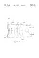
- FIG. 1Ashows a partially fabricated IC 10 that includes a tungsten layer 16, which is subjected to CMP to form tungsten plugs 24 as shown in FIG. 1B.
- CMPtypically involves mounting a substrate face down on a holder and rotating the substrate face against a polishing pad mounted on a pallet, which in turn is rotating or is in orbital state.
- a slurry containing a chemicale.g.
- an oxidizing agentsuch as Fe(NO 3 ) 3 , that chemically interacts with the tungsten layer and an abrasive, e.g. alumina (Al 2 O 3 ), that physically removes the tungsten layer, is flowed between the wafer and the polishing pad or on the pad near the substrate.
- FIG. 1Awhich shows partially fabricated IC 10 before the substrate surface undergoes CMP.
- a dielectric layer 12 disposed above a substrate surface 18 and having contact holes 14is filled with tungsten.
- a tungsten layer 16is also disposed atop dielectric layer 12.
- Some significant steps involved in forming the partially fabricated IC of FIG. 1Ainclude blanket depositing dielectric layer 12, such as SiO 2 , on substrate surface 18. After dielectric layer 12 is planarized, a masking layer (not shown), which typically includes photoresist, is blanket deposited over dielectric layer 12 and patterned by conventional photolithography. Next, the unmasked portions of dielectric layer 12 are etched to form contact holes 14 that provide an opening to the underlying substrate layer.
- tungsten layer 16is blanket deposited over the substrate surface, filling contact holes 14 with tungsten.
- tungstenmay be filled with a conductive titanium layer (not shown to simplify illustration) and a titanium nitride barrier layer (not shown to simplify illustration).
- viasmay be similarly etched to provide an opening in a dielectric layer that is disposed between two metallization layers and that metal plugs may be formed in such vias similarly.
- tungsten layer 16 of partially fabricated IC 10undergoes CMP, as described above, to form tungsten plugs by removing the tungsten layer deposited above the dielectric layer.
- FIG. 1Bwhich shows a partially fabricated IC 20 after undergoing CMP.
- Partially fated IChas tungsten plugs 26 formed in a dielectric layer 12 disposed atop a substrate 18.
- Fe(NO 3 ) 3oxidizes the tungsten to form tungsten oxide that is abraded by the alumina (Al 2 O 3 ) particles in the slurry. In this manner, the tungsten layer above the dielectric layer is removed to form tungsten plug 26 shown in FIG. 2.
- the top portion of the dielectric layermay fracture when the substrate surface is subjected to pressures as high as 10 psi and/or may also develop microcracks or scratches due to the abrasive action of the slurry.
- the iron residue from the slurrymigrates into the fissures and microcracks formed at the top portion of the dielectric layer, i.e. between about 50 and about 75 ⁇ ngstroms at the top of dielectric layer 12, and forms a contaminated dielectric layer 30.
- the removal of iron contaminants from contaminated layer 30is important because such contaminants lower the insulating properties of the dielectric layer, making the IC susceptible to catastrophic device failures.
- a current approachincludes treating the substrate surface after tungsten CMP with about 0.5% (by volume) hydrofluoric acid in deionized water to remove the iron contaminated dielectric layer.
- tungsten CMPtungsten CMP
- about 0.5% (by volume) hydrofluoric acid in deionized waterto remove the iron contaminated dielectric layer.
- prolonged exposure of the tungsten plug to a dilute hydrofluoric acid solutionresults in an increased likelihood of corrosion of the tungsten plug.
- Corrosionhas been identified in those plugs where a characteristic "seam” or a "keyhole” type structure typically formed near the middle region of the plug undergoes enlargement.
- the present inventionprovides a post metal chemical-mechanical polishing (CMP) cleaning process that effectively inhibits corrosion of a metallic plug.
- the processincludes providing a partially fabricated integrated circuit (IC) substrate having a metallic plug that is formed by subjecting a metallic surface on the integrated circuit (IC) substrate to chemical-mechanical polishing (CMP), which produces a contaminated dielectric layer containing metallic contaminants.
- CMPchemical-mechanical polishing
- the processalso includes scrubbing the IC substrate surface in the presence of a mixture including ethylene glycol and hydrofluoric acid to remove at least a portion of the contaminated dielectric layer and to effectively inhibit corrosion of the metallic plug.
- the mixturehas ethylene glycol in an amount that is between about 2 times and about 7 times the amount of hydrofluoric acid.
- the step of scrubbing described abovemay be carried out in a wafer scrubber where a brush contacts the substrate surface and mechanically removes at least a portion of the contaminated dielectric layer therefrom.
- the mixture of ethylene glycol and hydrofluoric acid employed abovemay include deionized water.
- the amount of ethylene glycolis preferably between about 2 times and about 5 times the amount of hydrofluoric acid.
- the corrosion inhibiting, cleaning process described abovemay further include a step of removing particle residues adhering to the substrate surface by scrubbing the substrate surface with a brush in the presence of sufficient amounts of ammonium hydroxide to produce an appropriate pH on the substrate surface that facilitates the separation of the particle residues from the substrate surface and the brush.
- the corrosion inhibiting process described abovemay further still include a step of performing a spin, rinse, dry cycle whereby the IC substrate surface is rinsed with deionized water to remove chemicals from the substrate surface and dried by exposing the IC substrate surface to a radiant heat source.
- the metal in the metal plug of the above described processis at least one selected from the group consisting of tungsten, aluminum and copper.
- the present inventionprovides a post tungsten CMP cleaning process that effectively inhibits corrosion of a tungsten plug.
- the processincludes providing a partially fabricated IC substrate having a tungsten plug that is formed by subjecting a tungsten layer on a surface of the IC substrate to chemical-mechanical polishing, which produces particle contaminants and a contaminated dielectric layer containing metallic contaminants.
- the processalso include a step of removing particle contaminants from the substrate surface by scrubbing with a brush the substrate surface in the presence of sufficient amounts of ammonium hydroxide such that a pH of about 9.5 and above is maintained above the substrate surface and whereby the particle contaminants separate from the substrate surface and the brush.
- the processfurther still includes scrubbing the IC substrate surface in the presence of a mixture including ethylene glycol and hydrofluoric acid to remove the contaminated dielectric layer and to effectively inhibit corrosion of the metallic plug.
- the mixturehas ethylene glycol in an amount that is between about 2 times and about 7 times the amount of hydrofluoric acid.
- the step of removing particle contaminantsmay include providing deionized water and about 2% by volume of ammonium hydroxide on the substrate surface.
- the step of scrubbingmay be carried out until between about 50 and about 100 ⁇ ngstroms of the contaminated dielectric layer is removed.
- the amount of hydrofluoric acid in the corrosion inhibiting mixturemay generally be between about 0.5% and about 1% by volume in the mixture and preferably be between about 0.5% by volume.
- the amount of ethylene glycol in the corrosion inhibiting mixturemay be between about 1% and about 7% by volume.
- the particle contaminantsmay include tungsten oxide and the metallic contaminants may include iron or potassium.
- the present inventionprovides a corrosion inhibiting composition for cleaning a partially fabricated IC having metallic plugs.
- the compositionincludes an effective amount of hydrofluoric acid to remove at least portions of a contaminated dielectric layer having metallic contaminants and an effective amount of ethylene glycol to inhibit corrosion of the metallic plug, wherein the amount of ethylene glycol is between about 2 times and about 7 times the amount of hydrofluoric acid.
- the corrosion inhibiting compositionmay further include deionized water.
- the amount of ethylene glycol in the compositionmay be between about 2 times and about 5 times the amount of the hydrofluoric acid.
- the amount of hydrofluoric acid in the compositionmay generally be between about 0.5% and about 1% by volume, may preferably be about 0.5% by volume.
- the amount of ethylene glycolmay generally be between about 1% and about 3.5% by volume and may preferably be between about 1% and about 2.5% by volume.
- the amount of ethylene glycol in the compositionmay generally be between about 1% and about 7% by volume.
- FIG. 1Ashows a partially fabricated integrated circuit (IC) before undergoing chemical-mechanical polishing (CMP).
- FIG. 1Bshows a partially fabricated IC that includes tungsten plugs formed by subjecting the partially fabricated IC of FIG. 1A to chemical-mechanical polishing (CMP).
- CMPchemical-mechanical polishing
- FIG. 2shows a simple schematic diagram of the major components in a wafer scrubber, which may be employed during post metal CMP cleaning steps, according to one embodiment of the present invention.
- FIG. 3shows a flowchart of a post tungsten CMP cleaning process, according to one embodiment of the present invention that uses ethylene glycol and hydrofluoric acid in a mixture to inhibiting corrosion of metal plugs.
- the present inventionprovides a composition and process for inhibiting corrosion in metal plugs that may result from post metal chemical-mechanical polishing (CMP) cleaning steps.
- CMPchemical-mechanical polishing
- the composition of the slurry employed during CMPmay include other oxidizing agents, besides ferric nitric (Fe(NO 3 ) 3 , such as hydrogen peroxide (H 2 O 2 ) and potassium iodate (KIO 3 ) to oxidize the metal composition of the plug.
- ferric nitricFe(NO 3 ) 3
- KIO 3potassium iodate
- the present inventionrecognizes the need for inhibiting corrosion in metal plugs that may result from post metal CMP cleaning steps.
- cleaning of a contaminated dielectric layer on an integrated circuit (IC) substrate surfaceis carried out by scrubbing the integrated circuit (IC) substrate surface in the presence of a corrosion inhibiting composition.
- the corrosion inhibiting composition of the present inventionincludes hydrofluoric acid and ethylene glycol to remove the contaminated dielectric layer and inhibit corrosion of the metal plug.
- Post metal CMP cleaning processes according to the present inventionmay be carried out in any wafer scrubber system.
- cleaning processes of the present inventionare carried out in a DSS 200 Series 2 Wafer Scrubber System, commercially available from OnTrak Systems, of San Jose, Calif.
- FIG. 2shows the major, relevant components of this wafer scrubber system. It should be borne in mind that the substrate cleaning process according to the present invention is not limited to any particular wafer scrubber configuration and that any chamber fitted with brushes to contact the substrate surface will work.
- Wafer scrubber system 200as shown in FIG. 2, may be configured to clean any IC substrate, however, it is preferably employed to clean semiconductor wafer substrates.
- System 200includes two brush boxes, a primary chamber 202 and a secondary chamber 206, and a spin, rinse, dry station 210.
- Each of chambers 202 and 206include double sided scrubbers, i.e. they come equipped with two brushes 205 (for chamber 202) and 207 (for chamber 206) mounted on top and two brushes 204 (for chamber 202 ) and 208 (for chamber 206) mounted on the bottom such that a substrate placed between the two sets of brushes 204 and 205 or 208 and 207 would have both of its surfaces. scrubbed or mechanically cleaned.
- Spin, rinse, dry station 212includes a chuck 212, upon which the substrate is secured to undergo rinsing and then drying by the radiant heat produced by bright lights (not shown to simplify illustration).
- FIG. 3shows a flowchart of one embodiment of the inventive post metal CMP cleaning processes that may be implemented in the wafer scrubber system of FIG. 2.
- the process of FIG. 3removes a contaminated dielectric layer, e.g., contaminated dielectric layer 30 of FIG. 1B, and effectively inhibits corrosion of metal plugs, e.g., tungsten plug 26 of FIG. 1B.
- a corrosion inhibiting cleaning process 300 of FIG. 3begins, a partially fabricated IC substrate like the one shown in FIG. 1B is formed by the process described above.
- Cleaning process 300may begin with a step 302, which includes removing particle contaminants from a surface of the partially fabricated IC substrate.
- the particle contaminants, such as metal oxides, removed in this steptypically originate from the slurry composition or may be part of the eroded material from the substrate surface during CMP. Typically such metal oxides adhere to the substrate surface due to the build up of electrostatic charge on the substrate surface.
- a cleaning mixtureis introduced inside primary chamber 202 of FIG. 2 to provide an appropriate pH on the substrate surface, and thereby effectively produce a zeta potential, also known in the art as an electrostatic potential, for the metal oxide, brushes 204 and 205 of FIG. 2 and the dielectric layer that facilitates the separation of the metal oxide from the dielectric layer and the brushes.
- tungsten oxide particlesproduced by tungsten CMP
- a cleaning mixture containing 2% (in volume) ammonium hydroxide (NH 4 OH) and deionized watermay be introduced inside primary chamber 202 of FIG. 2.
- the cleaning mixtureeffectively provides a pH on the substrate surface that is greater than or equal to about 9.5, which produces the necessary repulsion forces for the separation of tungsten oxide from the substrate surface and the brushes.
- the separated tungsten oxide particlesare removed from the substrate surface by the action of brushes 204 and 205 of FIG. 2. In this manner, the substrate surface is rendered clean of any particle contaminants, e.g. tungsten oxide, that may be produced during tungsten CMP.
- a contaminated dielectric layere.g., contaminated dielectric layer 30 of FIG. 1B, enriched with metal contaminants embedded into a dielectric layer during metal CMP, undergoes scrubbing in the presence of a corrosion inhibiting composition of a post metal CMP cleaning mixture.
- a corrosion inhibiting composition of a post metal CMP cleaning mixturee.g., one of brushes 207 and 208 scrub contaminated dielectric layer 30 of FIG. 1B on the substrate surface in the presence of a corrosion inhibiting composition.
- the corrosion inhibiting composition of the cleaning mixturecontains hydrofluoric acid, ethylene glycol and deionized water.
- Hydrofluoric acidmay generally be present in an effective amount, e.g. between about 0.5% and about 1%, in the mixture to facilitate the removal of the contaminated dielectric layer from the substrate surface.
- a cleaning mixture containing about 0.5% (in volume) of hydrofluoric acidmay effectively remove between about 50 and about 100 ⁇ ngstroms of the iron contaminated dielectric layer 30 of FIG. 1B.
- Ethylene glycolmay be present in effective amounts in the cleaning mixture to inhibit corrosion of the metal plug.
- the amount of ethylene glycol in the mixturewill vary depending on the concentration of by fluoric acid present in the cleaning mixture.
- the amount of ethylene glycol present in the mixturemay generally be between about 2 and about 7 times the amount of hydrofluoric acid present in the mixture and may preferably be between about 2 and about 5 times the amount of hydrofluoric acid present in the mixture.
- the amount of ethylene glycol in the mixturewill therefore be between about 1% and about 3.5% and preferably be between about 1% and about 2.5%.
- the amount of ethylene glycolwill be between about 2% and about 7% and preferably be between about 2% and about 5%.
- Step 304may be carried out until all of the contaminated dielectric layer is removed. According to the cleaning process of the present invention, scrubbing with the cleaning mixture inhibits the corrosion of the metal plug and the likelihood of degradation of the plug is reduced significantly.
- any chemical residue from the cleaning mixtures of steps 302 and 304 mentioned aboveare removed from the substrate surface by cleaning the substrate surface in spin, rinse, dry station 210 of FIG. 2.
- spin, rinse, dry station 210 of FIG. 2the substrate is secured on chuck 212 of FIG. 2 and sprayed with water to rinse off the chemicals on the substrate surface.
- the chuckswitches to a high speed rotation, which literally throws the water off the substrate surface.
- the substrate surfaceis then dried by the radiant heat that may be generated by bright lights (not shown to simplify illustration) mounted on top of station 210 of FIG. 2.
Landscapes
- Engineering & Computer Science (AREA)
- Microelectronics & Electronic Packaging (AREA)
- Condensed Matter Physics & Semiconductors (AREA)
- General Physics & Mathematics (AREA)
- Manufacturing & Machinery (AREA)
- Computer Hardware Design (AREA)
- Physics & Mathematics (AREA)
- Power Engineering (AREA)
- Chemical & Material Sciences (AREA)
- Materials Engineering (AREA)
- Mechanical Engineering (AREA)
- Metallurgy (AREA)
- Organic Chemistry (AREA)
- Cleaning Or Drying Semiconductors (AREA)
- Mechanical Treatment Of Semiconductor (AREA)
Abstract
Description
Claims (22)
Priority Applications (1)
| Application Number | Priority Date | Filing Date | Title |
|---|---|---|---|
| US08/918,483US5893756A (en) | 1997-08-26 | 1997-08-26 | Use of ethylene glycol as a corrosion inhibitor during cleaning after metal chemical mechanical polishing |
Applications Claiming Priority (1)
| Application Number | Priority Date | Filing Date | Title |
|---|---|---|---|
| US08/918,483US5893756A (en) | 1997-08-26 | 1997-08-26 | Use of ethylene glycol as a corrosion inhibitor during cleaning after metal chemical mechanical polishing |
Publications (1)
| Publication Number | Publication Date |
|---|---|
| US5893756Atrue US5893756A (en) | 1999-04-13 |
Family
ID=25440457
Family Applications (1)
| Application Number | Title | Priority Date | Filing Date |
|---|---|---|---|
| US08/918,483Expired - LifetimeUS5893756A (en) | 1997-08-26 | 1997-08-26 | Use of ethylene glycol as a corrosion inhibitor during cleaning after metal chemical mechanical polishing |
Country Status (1)
| Country | Link |
|---|---|
| US (1) | US5893756A (en) |
Cited By (88)
| Publication number | Priority date | Publication date | Assignee | Title |
|---|---|---|---|---|
| US6060370A (en)* | 1998-06-16 | 2000-05-09 | Lsi Logic Corporation | Method for shallow trench isolations with chemical-mechanical polishing |
| US6066266A (en)* | 1998-07-08 | 2000-05-23 | Lsi Logic Corporation | In-situ chemical-mechanical polishing slurry formulation for compensation of polish pad degradation |
| US6071818A (en)* | 1998-06-30 | 2000-06-06 | Lsi Logic Corporation | Endpoint detection method and apparatus which utilize an endpoint polishing layer of catalyst material |
| US6074517A (en)* | 1998-07-08 | 2000-06-13 | Lsi Logic Corporation | Method and apparatus for detecting an endpoint polishing layer by transmitting infrared light signals through a semiconductor wafer |
| US6077762A (en)* | 1997-12-22 | 2000-06-20 | Vlsi Technology, Inc. | Method and apparatus for rapidly discharging plasma etched interconnect structures |
| US6077783A (en)* | 1998-06-30 | 2000-06-20 | Lsi Logic Corporation | Method and apparatus for detecting a polishing endpoint based upon heat conducted through a semiconductor wafer |
| US6080670A (en)* | 1998-08-10 | 2000-06-27 | Lsi Logic Corporation | Method of detecting a polishing endpoint layer of a semiconductor wafer which includes a non-reactive reporting specie |
| US6093280A (en)* | 1997-08-18 | 2000-07-25 | Lsi Logic Corporation | Chemical-mechanical polishing pad conditioning systems |
| US6093658A (en)* | 1997-12-22 | 2000-07-25 | Philips Electronics North America Corporation | Method for making reliable interconnect structures |
| US6108093A (en)* | 1997-06-04 | 2000-08-22 | Lsi Logic Corporation | Automated inspection system for residual metal after chemical-mechanical polishing |
| US6106371A (en)* | 1997-10-30 | 2000-08-22 | Lsi Logic Corporation | Effective pad conditioning |
| US6115233A (en)* | 1996-06-28 | 2000-09-05 | Lsi Logic Corporation | Integrated circuit device having a capacitor with the dielectric peripheral region being greater than the dielectric central region |
| US6117779A (en) | 1998-12-15 | 2000-09-12 | Lsi Logic Corporation | Endpoint detection method and apparatus which utilize a chelating agent to detect a polishing endpoint |
| US6121147A (en)* | 1998-12-11 | 2000-09-19 | Lsi Logic Corporation | Apparatus and method of detecting a polishing endpoint layer of a semiconductor wafer which includes a metallic reporting substance |
| US6147002A (en)* | 1999-05-26 | 2000-11-14 | Ashland Inc. | Process for removing contaminant from a surface and composition useful therefor |
| US6153531A (en)* | 1997-12-22 | 2000-11-28 | Philips Electronics North America Corporation | Method for preventing electrochemical erosion of interconnect structures |
| US6168508B1 (en) | 1997-08-25 | 2001-01-02 | Lsi Logic Corporation | Polishing pad surface for improved process control |
| US6179956B1 (en) | 1998-01-09 | 2001-01-30 | Lsi Logic Corporation | Method and apparatus for using across wafer back pressure differentials to influence the performance of chemical mechanical polishing |
| US6197690B1 (en)* | 1998-12-04 | 2001-03-06 | Advanced Micro Devices, Inc. | Chemically preventing Cu dendrite formation and growth by double sided scrubbing |
| US6200899B1 (en)* | 1998-04-30 | 2001-03-13 | International Business Machines Corporation | Method of cleaning semiconductor wafers after CMP planarization |
| US6201253B1 (en) | 1998-10-22 | 2001-03-13 | Lsi Logic Corporation | Method and apparatus for detecting a planarized outer layer of a semiconductor wafer with a confocal optical system |
| US6234883B1 (en) | 1997-10-01 | 2001-05-22 | Lsi Logic Corporation | Method and apparatus for concurrent pad conditioning and wafer buff in chemical mechanical polishing |
| US6241847B1 (en) | 1998-06-30 | 2001-06-05 | Lsi Logic Corporation | Method and apparatus for detecting a polishing endpoint based upon infrared signals |
| US6268224B1 (en) | 1998-06-30 | 2001-07-31 | Lsi Logic Corporation | Method and apparatus for detecting an ion-implanted polishing endpoint layer within a semiconductor wafer |
| US6274478B1 (en)* | 1999-07-13 | 2001-08-14 | Motorola, Inc. | Method for forming a copper interconnect using a multi-platen chemical mechanical polishing (CMP) process |
| US6277753B1 (en)* | 1998-09-28 | 2001-08-21 | Supercritical Systems Inc. | Removal of CMP residue from semiconductors using supercritical carbon dioxide process |
| US6285035B1 (en) | 1998-07-08 | 2001-09-04 | Lsi Logic Corporation | Apparatus for detecting an endpoint polishing layer of a semiconductor wafer having a wafer carrier with independent concentric sub-carriers and associated method |
| US6286525B1 (en)* | 1997-05-08 | 2001-09-11 | Dainippon Screen Mfg. Co. | Substrate cleaning apparatus and method |
| US6297558B1 (en) | 1997-07-23 | 2001-10-02 | Lsi Logic Corporation | Slurry filling a recess formed during semiconductor fabrication |
| US6319836B1 (en) | 2000-09-26 | 2001-11-20 | Lsi Logic Corporation | Planarization system |
| US6319833B1 (en)* | 1998-12-07 | 2001-11-20 | Advanced Micro Devices, Inc. | Chemically preventing copper dendrite formation and growth by spraying |
| US6340434B1 (en) | 1997-09-05 | 2002-01-22 | Lsi Logic Corporation | Method and apparatus for chemical-mechanical polishing |
| US6375550B1 (en) | 2000-06-05 | 2002-04-23 | Lsi Logic Corporation | Method and apparatus for enhancing uniformity during polishing of a semiconductor wafer |
| US6391768B1 (en) | 2000-10-30 | 2002-05-21 | Lsi Logic Corporation | Process for CMP removal of excess trench or via filler metal which inhibits formation of concave regions on oxide surface of integrated circuit structure |
| US6432815B2 (en)* | 1998-12-21 | 2002-08-13 | Mitsubishi Denki Kabushiki Kaisha | Method of cleaning a silicon substrate after blanket depositing a tungsten film by dipping in a solution having hydrofluoric acid, hydrochloric acid, and/or ammonium hydroxide prior to patterning the tungsten film |
| US6439981B1 (en) | 2000-12-28 | 2002-08-27 | Lsi Logic Corporation | Arrangement and method for polishing a surface of a semiconductor wafer |
| US6451699B1 (en) | 1999-07-30 | 2002-09-17 | Lsi Logic Corporation | Method and apparatus for planarizing a wafer surface of a semiconductor wafer having an elevated portion extending therefrom |
| US6464566B1 (en) | 2000-06-29 | 2002-10-15 | Lsi Logic Corporation | Apparatus and method for linearly planarizing a surface of a semiconductor wafer |
| DE10118155A1 (en)* | 2001-04-03 | 2002-10-24 | Promos Technologies Inc | Removal of solid particles from polished surface coated with dielectric, used in integrated circuit production, uses cleaning with brush and etching with liquid to loosen embedded particles and further cleaning |
| US6475914B2 (en)* | 2000-07-22 | 2002-11-05 | Samsung Electronics Co., Ltd. | Method of manufacturing semiconductor device for protecting Cu layer from post chemical mechanical polishing-corrosion |
| US6489242B1 (en) | 2000-09-13 | 2002-12-03 | Lsi Logic Corporation | Process for planarization of integrated circuit structure which inhibits cracking of low dielectric constant dielectric material adjacent underlying raised structures |
| US6528389B1 (en) | 1998-12-17 | 2003-03-04 | Lsi Logic Corporation | Substrate planarization with a chemical mechanical polishing stop layer |
| US20030049935A1 (en)* | 2001-05-04 | 2003-03-13 | Promos Technologies Inc. | Method for removing residual particles from a polished surface |
| US6541383B1 (en) | 2000-06-29 | 2003-04-01 | Lsi Logic Corporation | Apparatus and method for planarizing the surface of a semiconductor wafer |
| US20030077983A1 (en)* | 2001-10-12 | 2003-04-24 | International Business Machines Corporation | Cleaning polish etch composition and process for a superfinished surface of a substrate |
| US6573173B2 (en) | 1999-07-13 | 2003-06-03 | Motorola, Inc. | Method for forming a copper interconnect using a multi-platen chemical mechanical polishing (CMP) process |
| US6585567B1 (en) | 2001-08-31 | 2003-07-01 | Koninklijke Philips Electronics N.V. | Short CMP polish method |
| US6607967B1 (en) | 2000-11-15 | 2003-08-19 | Lsi Logic Corporation | Process for forming planarized isolation trench in integrated circuit structure on semiconductor substrate |
| US6638145B2 (en) | 2001-08-31 | 2003-10-28 | Koninklijke Philips Electronics N.V. | Constant pH polish and scrub |
| US6703301B2 (en) | 2002-04-26 | 2004-03-09 | Macronix International Co., Ltd. | Method of preventing tungsten plugs from corrosion |
| US6705930B2 (en) | 2000-01-28 | 2004-03-16 | Lam Research Corporation | System and method for polishing and planarizing semiconductor wafers using reduced surface area polishing pads and variable partial pad-wafer overlapping techniques |
| US6729943B2 (en) | 2000-01-28 | 2004-05-04 | Lam Research Corporation | System and method for controlled polishing and planarization of semiconductor wafers |
| US6736701B1 (en) | 2001-11-20 | 2004-05-18 | Taiwan Semiconductor Manufacturing Company | Eliminate broken line damage of copper after CMP |
| US6756316B1 (en) | 1997-12-22 | 2004-06-29 | Koninklijke Philips Electronics N.V. | Semiconductor pressure transducer structures and methods for making the same |
| US6818546B2 (en)* | 2000-05-08 | 2004-11-16 | Renesas Technology Corp. | Semiconductor integrated circuit device and a method of manufacturing the same |
| US20050008980A1 (en)* | 2002-02-15 | 2005-01-13 | Arena-Foster Chantal J. | Developing photoresist with supercritical fluid and developer |
| US20050064608A1 (en)* | 2003-09-03 | 2005-03-24 | Patel Nital S. | Versatile system for controlling semiconductor topography |
| US6890853B2 (en) | 2000-04-25 | 2005-05-10 | Tokyo Electron Limited | Method of depositing metal film and metal deposition cluster tool including supercritical drying/cleaning module |
| US6928746B2 (en) | 2002-02-15 | 2005-08-16 | Tokyo Electron Limited | Drying resist with a solvent bath and supercritical CO2 |
| US20060003521A1 (en)* | 2003-06-02 | 2006-01-05 | Akira Fukunaga | Method of and apparatus for manufacturing semiconductor device |
| US20060003592A1 (en)* | 2004-06-30 | 2006-01-05 | Tokyo Electron Limited | System and method for processing a substrate using supercritical carbon dioxide processing |
| US20060068583A1 (en)* | 2004-09-29 | 2006-03-30 | Tokyo Electron Limited | A method for supercritical carbon dioxide processing of fluoro-carbon films |
| US20060102208A1 (en)* | 2004-11-12 | 2006-05-18 | Tokyo Electron Limited | System for removing a residue from a substrate using supercritical carbon dioxide processing |
| US20060102204A1 (en)* | 2004-11-12 | 2006-05-18 | Tokyo Electron Limited | Method for removing a residue from a substrate using supercritical carbon dioxide processing |
| US20060104831A1 (en)* | 2004-11-12 | 2006-05-18 | Tokyo Electron Limited | Method and system for cooling a pump |
| US20060102590A1 (en)* | 2004-11-12 | 2006-05-18 | Tokyo Electron Limited | Method for treating a substrate with a high pressure fluid using a preoxide-based process chemistry |
| US20060102591A1 (en)* | 2004-11-12 | 2006-05-18 | Tokyo Electron Limited | Method and system for treating a substrate using a supercritical fluid |
| US7064070B2 (en) | 1998-09-28 | 2006-06-20 | Tokyo Electron Limited | Removal of CMP and post-CMP residue from semiconductors using supercritical carbon dioxide process |
| US20060180174A1 (en)* | 2005-02-15 | 2006-08-17 | Tokyo Electron Limited | Method and system for treating a substrate with a high pressure fluid using a peroxide-based process chemistry in conjunction with an initiator |
| US20060180572A1 (en)* | 2005-02-15 | 2006-08-17 | Tokyo Electron Limited | Removal of post etch residue for a substrate with open metal surfaces |
| US20060180573A1 (en)* | 2005-02-15 | 2006-08-17 | Tokyo Electron Limited | Method and system for treating a substrate with a high pressure fluid using fluorosilicic acid |
| US20060255012A1 (en)* | 2005-05-10 | 2006-11-16 | Gunilla Jacobson | Removal of particles from substrate surfaces using supercritical processing |
| US20060254615A1 (en)* | 2005-05-13 | 2006-11-16 | Tokyo Electron Limited | Treatment of substrate using functionalizing agent in supercritical carbon dioxide |
| US7163380B2 (en) | 2003-07-29 | 2007-01-16 | Tokyo Electron Limited | Control of fluid flow in the processing of an object with a fluid |
| US20070012337A1 (en)* | 2005-07-15 | 2007-01-18 | Tokyo Electron Limited | In-line metrology for supercritical fluid processing |
| US7169540B2 (en) | 2002-04-12 | 2007-01-30 | Tokyo Electron Limited | Method of treatment of porous dielectric films to reduce damage during cleaning |
| US7270941B2 (en) | 2002-03-04 | 2007-09-18 | Tokyo Electron Limited | Method of passivating of low dielectric materials in wafer processing |
| US7387868B2 (en) | 2002-03-04 | 2008-06-17 | Tokyo Electron Limited | Treatment of a dielectric layer using supercritical CO2 |
| US7399708B2 (en) | 2005-03-30 | 2008-07-15 | Tokyo Electron Limited | Method of treating a composite spin-on glass/anti-reflective material prior to cleaning |
| US20080221004A1 (en)* | 2005-05-25 | 2008-09-11 | Freescale Semiconductor, Inc. | Cleaning Solution for a Semiconductor Wafer |
| US7442636B2 (en) | 2005-03-30 | 2008-10-28 | Tokyo Electron Limited | Method of inhibiting copper corrosion during supercritical CO2 cleaning |
| DE102007030957A1 (en)* | 2007-07-04 | 2009-01-08 | Siltronic Ag | Method for cleaning a semiconductor wafer with a cleaning solution |
| US7550075B2 (en) | 2005-03-23 | 2009-06-23 | Tokyo Electron Ltd. | Removal of contaminants from a fluid |
| US7751609B1 (en) | 2000-04-20 | 2010-07-06 | Lsi Logic Corporation | Determination of film thickness during chemical mechanical polishing |
| US20100229890A1 (en)* | 2009-03-10 | 2010-09-16 | Lam Research Corp. | Method of Particle Contaminant Removal |
| US20100273330A1 (en)* | 2006-08-23 | 2010-10-28 | Citibank N.A. As Collateral Agent | Rinse formulation for use in the manufacture of an integrated circuit |
| EP2205776A4 (en)* | 2007-09-13 | 2012-02-29 | Borregaard Ind | Corrosion inhibitor |
| US20180151427A1 (en)* | 2016-11-29 | 2018-05-31 | Taiwan Semiconductor Manufacturing Company, Ltd. | Method of Cleaning Wafer After CMP |
Citations (5)
| Publication number | Priority date | Publication date | Assignee | Title |
|---|---|---|---|---|
| US5389194A (en)* | 1993-02-05 | 1995-02-14 | Lsi Logic Corporation | Methods of cleaning semiconductor substrates after polishing |
| US5478436A (en)* | 1994-12-27 | 1995-12-26 | Motorola, Inc. | Selective cleaning process for fabricating a semiconductor device |
| US5545076A (en)* | 1994-05-16 | 1996-08-13 | Samsung Electronics Co., Ltd. | Apparatus for gringing a semiconductor wafer while removing dust therefrom |
| US5770095A (en)* | 1994-07-12 | 1998-06-23 | Kabushiki Kaisha Toshiba | Polishing agent and polishing method using the same |
| US5773364A (en)* | 1996-10-21 | 1998-06-30 | Motorola, Inc. | Method for using ammonium salt slurries for chemical mechanical polishing (CMP) |
- 1997
- 1997-08-26USUS08/918,483patent/US5893756A/ennot_activeExpired - Lifetime
Patent Citations (5)
| Publication number | Priority date | Publication date | Assignee | Title |
|---|---|---|---|---|
| US5389194A (en)* | 1993-02-05 | 1995-02-14 | Lsi Logic Corporation | Methods of cleaning semiconductor substrates after polishing |
| US5545076A (en)* | 1994-05-16 | 1996-08-13 | Samsung Electronics Co., Ltd. | Apparatus for gringing a semiconductor wafer while removing dust therefrom |
| US5770095A (en)* | 1994-07-12 | 1998-06-23 | Kabushiki Kaisha Toshiba | Polishing agent and polishing method using the same |
| US5478436A (en)* | 1994-12-27 | 1995-12-26 | Motorola, Inc. | Selective cleaning process for fabricating a semiconductor device |
| US5773364A (en)* | 1996-10-21 | 1998-06-30 | Motorola, Inc. | Method for using ammonium salt slurries for chemical mechanical polishing (CMP) |
Non-Patent Citations (2)
| Title |
|---|
| Presentation slides at CMPUG Annual Symposium, entitled "Alumina-SiO2 Interactions Under Conditions Relevant to Post-CMP Cleaning of W-Slurries", by I.J. Malik, R. Emami, C. Raghunath, and S. Raghavan of OnTrak Systems, Inc., Milpitas, California, Dec. 1996. |
| Presentation slides at CMPUG Annual Symposium, entitled Alumina SiO 2 Interactions Under Conditions Relevant to Post CMP Cleaning of W Slurries , by I.J. Malik, R. Emami, C. Raghunath, and S. Raghavan of OnTrak Systems, Inc., Milpitas, California, Dec. 1996.* |
Cited By (127)
| Publication number | Priority date | Publication date | Assignee | Title |
|---|---|---|---|---|
| US6115233A (en)* | 1996-06-28 | 2000-09-05 | Lsi Logic Corporation | Integrated circuit device having a capacitor with the dielectric peripheral region being greater than the dielectric central region |
| US6286525B1 (en)* | 1997-05-08 | 2001-09-11 | Dainippon Screen Mfg. Co. | Substrate cleaning apparatus and method |
| US6108093A (en)* | 1997-06-04 | 2000-08-22 | Lsi Logic Corporation | Automated inspection system for residual metal after chemical-mechanical polishing |
| US6297558B1 (en) | 1997-07-23 | 2001-10-02 | Lsi Logic Corporation | Slurry filling a recess formed during semiconductor fabrication |
| US6093280A (en)* | 1997-08-18 | 2000-07-25 | Lsi Logic Corporation | Chemical-mechanical polishing pad conditioning systems |
| US6168508B1 (en) | 1997-08-25 | 2001-01-02 | Lsi Logic Corporation | Polishing pad surface for improved process control |
| US6340434B1 (en) | 1997-09-05 | 2002-01-22 | Lsi Logic Corporation | Method and apparatus for chemical-mechanical polishing |
| US6234883B1 (en) | 1997-10-01 | 2001-05-22 | Lsi Logic Corporation | Method and apparatus for concurrent pad conditioning and wafer buff in chemical mechanical polishing |
| US6106371A (en)* | 1997-10-30 | 2000-08-22 | Lsi Logic Corporation | Effective pad conditioning |
| US6077762A (en)* | 1997-12-22 | 2000-06-20 | Vlsi Technology, Inc. | Method and apparatus for rapidly discharging plasma etched interconnect structures |
| US6093658A (en)* | 1997-12-22 | 2000-07-25 | Philips Electronics North America Corporation | Method for making reliable interconnect structures |
| US6756316B1 (en) | 1997-12-22 | 2004-06-29 | Koninklijke Philips Electronics N.V. | Semiconductor pressure transducer structures and methods for making the same |
| US6153531A (en)* | 1997-12-22 | 2000-11-28 | Philips Electronics North America Corporation | Method for preventing electrochemical erosion of interconnect structures |
| US6531397B1 (en) | 1998-01-09 | 2003-03-11 | Lsi Logic Corporation | Method and apparatus for using across wafer back pressure differentials to influence the performance of chemical mechanical polishing |
| US6179956B1 (en) | 1998-01-09 | 2001-01-30 | Lsi Logic Corporation | Method and apparatus for using across wafer back pressure differentials to influence the performance of chemical mechanical polishing |
| US6200899B1 (en)* | 1998-04-30 | 2001-03-13 | International Business Machines Corporation | Method of cleaning semiconductor wafers after CMP planarization |
| US6060370A (en)* | 1998-06-16 | 2000-05-09 | Lsi Logic Corporation | Method for shallow trench isolations with chemical-mechanical polishing |
| US6424019B1 (en) | 1998-06-16 | 2002-07-23 | Lsi Logic Corporation | Shallow trench isolation chemical-mechanical polishing process |
| US6241847B1 (en) | 1998-06-30 | 2001-06-05 | Lsi Logic Corporation | Method and apparatus for detecting a polishing endpoint based upon infrared signals |
| US6077783A (en)* | 1998-06-30 | 2000-06-20 | Lsi Logic Corporation | Method and apparatus for detecting a polishing endpoint based upon heat conducted through a semiconductor wafer |
| US6268224B1 (en) | 1998-06-30 | 2001-07-31 | Lsi Logic Corporation | Method and apparatus for detecting an ion-implanted polishing endpoint layer within a semiconductor wafer |
| US6258205B1 (en) | 1998-06-30 | 2001-07-10 | Lsi Logic Corporation | Endpoint detection method and apparatus which utilize an endpoint polishing layer of catalyst material |
| US6071818A (en)* | 1998-06-30 | 2000-06-06 | Lsi Logic Corporation | Endpoint detection method and apparatus which utilize an endpoint polishing layer of catalyst material |
| US6066266A (en)* | 1998-07-08 | 2000-05-23 | Lsi Logic Corporation | In-situ chemical-mechanical polishing slurry formulation for compensation of polish pad degradation |
| US6074517A (en)* | 1998-07-08 | 2000-06-13 | Lsi Logic Corporation | Method and apparatus for detecting an endpoint polishing layer by transmitting infrared light signals through a semiconductor wafer |
| US6285035B1 (en) | 1998-07-08 | 2001-09-04 | Lsi Logic Corporation | Apparatus for detecting an endpoint polishing layer of a semiconductor wafer having a wafer carrier with independent concentric sub-carriers and associated method |
| US6080670A (en)* | 1998-08-10 | 2000-06-27 | Lsi Logic Corporation | Method of detecting a polishing endpoint layer of a semiconductor wafer which includes a non-reactive reporting specie |
| US6277753B1 (en)* | 1998-09-28 | 2001-08-21 | Supercritical Systems Inc. | Removal of CMP residue from semiconductors using supercritical carbon dioxide process |
| US7064070B2 (en) | 1998-09-28 | 2006-06-20 | Tokyo Electron Limited | Removal of CMP and post-CMP residue from semiconductors using supercritical carbon dioxide process |
| US6201253B1 (en) | 1998-10-22 | 2001-03-13 | Lsi Logic Corporation | Method and apparatus for detecting a planarized outer layer of a semiconductor wafer with a confocal optical system |
| US6354908B2 (en) | 1998-10-22 | 2002-03-12 | Lsi Logic Corp. | Method and apparatus for detecting a planarized outer layer of a semiconductor wafer with a confocal optical system |
| US6197690B1 (en)* | 1998-12-04 | 2001-03-06 | Advanced Micro Devices, Inc. | Chemically preventing Cu dendrite formation and growth by double sided scrubbing |
| US6319833B1 (en)* | 1998-12-07 | 2001-11-20 | Advanced Micro Devices, Inc. | Chemically preventing copper dendrite formation and growth by spraying |
| US6121147A (en)* | 1998-12-11 | 2000-09-19 | Lsi Logic Corporation | Apparatus and method of detecting a polishing endpoint layer of a semiconductor wafer which includes a metallic reporting substance |
| US6117779A (en) | 1998-12-15 | 2000-09-12 | Lsi Logic Corporation | Endpoint detection method and apparatus which utilize a chelating agent to detect a polishing endpoint |
| US6383332B1 (en) | 1998-12-15 | 2002-05-07 | Lsi Logic Corporation | Endpoint detection method and apparatus which utilize a chelating agent to detect a polishing endpoint |
| US6528389B1 (en) | 1998-12-17 | 2003-03-04 | Lsi Logic Corporation | Substrate planarization with a chemical mechanical polishing stop layer |
| US6432815B2 (en)* | 1998-12-21 | 2002-08-13 | Mitsubishi Denki Kabushiki Kaisha | Method of cleaning a silicon substrate after blanket depositing a tungsten film by dipping in a solution having hydrofluoric acid, hydrochloric acid, and/or ammonium hydroxide prior to patterning the tungsten film |
| US6596630B2 (en) | 1998-12-21 | 2003-07-22 | Mitsubishi Denki Kabushiki Kaisha | Method of cleaning a silicon substrate after blanket depositing a tungsten film by dipping in a solution of hydrofluoric acid, hydrochloric acid, and/or ammonium hydroxide |
| US6147002A (en)* | 1999-05-26 | 2000-11-14 | Ashland Inc. | Process for removing contaminant from a surface and composition useful therefor |
| US6274478B1 (en)* | 1999-07-13 | 2001-08-14 | Motorola, Inc. | Method for forming a copper interconnect using a multi-platen chemical mechanical polishing (CMP) process |
| US6444569B2 (en) | 1999-07-13 | 2002-09-03 | Motorola, Inc. | Method for forming a copper interconnect using a multi-platen chemical mechanical polishing (CMP) process |
| US6573173B2 (en) | 1999-07-13 | 2003-06-03 | Motorola, Inc. | Method for forming a copper interconnect using a multi-platen chemical mechanical polishing (CMP) process |
| US6451699B1 (en) | 1999-07-30 | 2002-09-17 | Lsi Logic Corporation | Method and apparatus for planarizing a wafer surface of a semiconductor wafer having an elevated portion extending therefrom |
| US6729943B2 (en) | 2000-01-28 | 2004-05-04 | Lam Research Corporation | System and method for controlled polishing and planarization of semiconductor wafers |
| US20040166782A1 (en)* | 2000-01-28 | 2004-08-26 | Lam Research Corporation. | System and method for polishing and planarizing semiconductor wafers using reduced surface area polishing pads and variable partial pad-wafer overlapping techniques |
| US6869337B2 (en) | 2000-01-28 | 2005-03-22 | Lam Research Corporation | System and method for polishing and planarizing semiconductor wafers using reduced surface area polishing pads and variable partial pad-wafer overlapping techniques |
| US6705930B2 (en) | 2000-01-28 | 2004-03-16 | Lam Research Corporation | System and method for polishing and planarizing semiconductor wafers using reduced surface area polishing pads and variable partial pad-wafer overlapping techniques |
| US7751609B1 (en) | 2000-04-20 | 2010-07-06 | Lsi Logic Corporation | Determination of film thickness during chemical mechanical polishing |
| US6890853B2 (en) | 2000-04-25 | 2005-05-10 | Tokyo Electron Limited | Method of depositing metal film and metal deposition cluster tool including supercritical drying/cleaning module |
| US7208411B2 (en) | 2000-04-25 | 2007-04-24 | Tokyo Electron Limited | Method of depositing metal film and metal deposition cluster tool including supercritical drying/cleaning module |
| US20050095844A1 (en)* | 2000-05-08 | 2005-05-05 | Tatsuyuki Saito | Semiconductor integrated circuit device |
| US7642652B2 (en) | 2000-05-08 | 2010-01-05 | Renesas Technology Corp. | Semiconductor integrated circuit device and a method of manufacturing the same |
| US20080042282A1 (en)* | 2000-05-08 | 2008-02-21 | Tatsuyuki Saito | Semiconductor integrated circuit device and a method of manufacturing the same |
| US7321171B2 (en) | 2000-05-08 | 2008-01-22 | Renesas Technology Corp. | Semiconductor integrated circuit device |
| KR100779295B1 (en)* | 2000-05-08 | 2007-11-23 | 가부시키가이샤 히타치세이사쿠쇼 | Semiconductor integrated circuit device and manufacturing method thereof |
| US6818546B2 (en)* | 2000-05-08 | 2004-11-16 | Renesas Technology Corp. | Semiconductor integrated circuit device and a method of manufacturing the same |
| US6375550B1 (en) | 2000-06-05 | 2002-04-23 | Lsi Logic Corporation | Method and apparatus for enhancing uniformity during polishing of a semiconductor wafer |
| US6464566B1 (en) | 2000-06-29 | 2002-10-15 | Lsi Logic Corporation | Apparatus and method for linearly planarizing a surface of a semiconductor wafer |
| US6541383B1 (en) | 2000-06-29 | 2003-04-01 | Lsi Logic Corporation | Apparatus and method for planarizing the surface of a semiconductor wafer |
| US6475914B2 (en)* | 2000-07-22 | 2002-11-05 | Samsung Electronics Co., Ltd. | Method of manufacturing semiconductor device for protecting Cu layer from post chemical mechanical polishing-corrosion |
| US6489242B1 (en) | 2000-09-13 | 2002-12-03 | Lsi Logic Corporation | Process for planarization of integrated circuit structure which inhibits cracking of low dielectric constant dielectric material adjacent underlying raised structures |
| US6713394B2 (en) | 2000-09-13 | 2004-03-30 | Lsi Logic Corporation | Process for planarization of integrated circuit structure which inhibits cracking of low dielectric constant dielectric material adjacent underlying raised structures |
| US6319836B1 (en) | 2000-09-26 | 2001-11-20 | Lsi Logic Corporation | Planarization system |
| US6391768B1 (en) | 2000-10-30 | 2002-05-21 | Lsi Logic Corporation | Process for CMP removal of excess trench or via filler metal which inhibits formation of concave regions on oxide surface of integrated circuit structure |
| US6607967B1 (en) | 2000-11-15 | 2003-08-19 | Lsi Logic Corporation | Process for forming planarized isolation trench in integrated circuit structure on semiconductor substrate |
| US6555475B1 (en) | 2000-12-28 | 2003-04-29 | Lsi Logic Corporation | Arrangement and method for polishing a surface of a semiconductor wafer |
| US6439981B1 (en) | 2000-12-28 | 2002-08-27 | Lsi Logic Corporation | Arrangement and method for polishing a surface of a semiconductor wafer |
| DE10118155A1 (en)* | 2001-04-03 | 2002-10-24 | Promos Technologies Inc | Removal of solid particles from polished surface coated with dielectric, used in integrated circuit production, uses cleaning with brush and etching with liquid to loosen embedded particles and further cleaning |
| US20030049935A1 (en)* | 2001-05-04 | 2003-03-13 | Promos Technologies Inc. | Method for removing residual particles from a polished surface |
| US6638145B2 (en) | 2001-08-31 | 2003-10-28 | Koninklijke Philips Electronics N.V. | Constant pH polish and scrub |
| US20040058546A1 (en)* | 2001-08-31 | 2004-03-25 | Hall Stacy W. | Constant pH polish and scrub |
| US6585567B1 (en) | 2001-08-31 | 2003-07-01 | Koninklijke Philips Electronics N.V. | Short CMP polish method |
| US6875089B2 (en)* | 2001-08-31 | 2005-04-05 | Koninklijke Philips Electronics N.V. | Constant pH polish and scrub |
| US20030077983A1 (en)* | 2001-10-12 | 2003-04-24 | International Business Machines Corporation | Cleaning polish etch composition and process for a superfinished surface of a substrate |
| US6736701B1 (en) | 2001-11-20 | 2004-05-18 | Taiwan Semiconductor Manufacturing Company | Eliminate broken line damage of copper after CMP |
| US20050008980A1 (en)* | 2002-02-15 | 2005-01-13 | Arena-Foster Chantal J. | Developing photoresist with supercritical fluid and developer |
| US6924086B1 (en) | 2002-02-15 | 2005-08-02 | Tokyo Electron Limited | Developing photoresist with supercritical fluid and developer |
| US7044662B2 (en) | 2002-02-15 | 2006-05-16 | Tokyo Electron Limited | Developing photoresist with supercritical fluid and developer |
| US6928746B2 (en) | 2002-02-15 | 2005-08-16 | Tokyo Electron Limited | Drying resist with a solvent bath and supercritical CO2 |
| US7270941B2 (en) | 2002-03-04 | 2007-09-18 | Tokyo Electron Limited | Method of passivating of low dielectric materials in wafer processing |
| US7387868B2 (en) | 2002-03-04 | 2008-06-17 | Tokyo Electron Limited | Treatment of a dielectric layer using supercritical CO2 |
| US7169540B2 (en) | 2002-04-12 | 2007-01-30 | Tokyo Electron Limited | Method of treatment of porous dielectric films to reduce damage during cleaning |
| US6703301B2 (en) | 2002-04-26 | 2004-03-09 | Macronix International Co., Ltd. | Method of preventing tungsten plugs from corrosion |
| US20060003521A1 (en)* | 2003-06-02 | 2006-01-05 | Akira Fukunaga | Method of and apparatus for manufacturing semiconductor device |
| US7163380B2 (en) | 2003-07-29 | 2007-01-16 | Tokyo Electron Limited | Control of fluid flow in the processing of an object with a fluid |
| US20050064608A1 (en)* | 2003-09-03 | 2005-03-24 | Patel Nital S. | Versatile system for controlling semiconductor topography |
| US7010381B2 (en)* | 2003-09-03 | 2006-03-07 | Texas Instruments Incorporated | Versatile system for controlling semiconductor topography |
| US7250374B2 (en) | 2004-06-30 | 2007-07-31 | Tokyo Electron Limited | System and method for processing a substrate using supercritical carbon dioxide processing |
| US20060003592A1 (en)* | 2004-06-30 | 2006-01-05 | Tokyo Electron Limited | System and method for processing a substrate using supercritical carbon dioxide processing |
| US7307019B2 (en) | 2004-09-29 | 2007-12-11 | Tokyo Electron Limited | Method for supercritical carbon dioxide processing of fluoro-carbon films |
| US20060068583A1 (en)* | 2004-09-29 | 2006-03-30 | Tokyo Electron Limited | A method for supercritical carbon dioxide processing of fluoro-carbon films |
| US20060102204A1 (en)* | 2004-11-12 | 2006-05-18 | Tokyo Electron Limited | Method for removing a residue from a substrate using supercritical carbon dioxide processing |
| US7491036B2 (en) | 2004-11-12 | 2009-02-17 | Tokyo Electron Limited | Method and system for cooling a pump |
| US20060102591A1 (en)* | 2004-11-12 | 2006-05-18 | Tokyo Electron Limited | Method and system for treating a substrate using a supercritical fluid |
| US20060102590A1 (en)* | 2004-11-12 | 2006-05-18 | Tokyo Electron Limited | Method for treating a substrate with a high pressure fluid using a preoxide-based process chemistry |
| US20060104831A1 (en)* | 2004-11-12 | 2006-05-18 | Tokyo Electron Limited | Method and system for cooling a pump |
| US20060102208A1 (en)* | 2004-11-12 | 2006-05-18 | Tokyo Electron Limited | System for removing a residue from a substrate using supercritical carbon dioxide processing |
| US20060180174A1 (en)* | 2005-02-15 | 2006-08-17 | Tokyo Electron Limited | Method and system for treating a substrate with a high pressure fluid using a peroxide-based process chemistry in conjunction with an initiator |
| US7291565B2 (en) | 2005-02-15 | 2007-11-06 | Tokyo Electron Limited | Method and system for treating a substrate with a high pressure fluid using fluorosilicic acid |
| US20060180572A1 (en)* | 2005-02-15 | 2006-08-17 | Tokyo Electron Limited | Removal of post etch residue for a substrate with open metal surfaces |
| US20060180573A1 (en)* | 2005-02-15 | 2006-08-17 | Tokyo Electron Limited | Method and system for treating a substrate with a high pressure fluid using fluorosilicic acid |
| US7550075B2 (en) | 2005-03-23 | 2009-06-23 | Tokyo Electron Ltd. | Removal of contaminants from a fluid |
| US7399708B2 (en) | 2005-03-30 | 2008-07-15 | Tokyo Electron Limited | Method of treating a composite spin-on glass/anti-reflective material prior to cleaning |
| US7442636B2 (en) | 2005-03-30 | 2008-10-28 | Tokyo Electron Limited | Method of inhibiting copper corrosion during supercritical CO2 cleaning |
| US20060255012A1 (en)* | 2005-05-10 | 2006-11-16 | Gunilla Jacobson | Removal of particles from substrate surfaces using supercritical processing |
| US20060254615A1 (en)* | 2005-05-13 | 2006-11-16 | Tokyo Electron Limited | Treatment of substrate using functionalizing agent in supercritical carbon dioxide |
| US7789971B2 (en) | 2005-05-13 | 2010-09-07 | Tokyo Electron Limited | Treatment of substrate using functionalizing agent in supercritical carbon dioxide |
| US7939482B2 (en) | 2005-05-25 | 2011-05-10 | Freescale Semiconductor, Inc. | Cleaning solution for a semiconductor wafer |
| US20080221004A1 (en)* | 2005-05-25 | 2008-09-11 | Freescale Semiconductor, Inc. | Cleaning Solution for a Semiconductor Wafer |
| US20070012337A1 (en)* | 2005-07-15 | 2007-01-18 | Tokyo Electron Limited | In-line metrology for supercritical fluid processing |
| US20100273330A1 (en)* | 2006-08-23 | 2010-10-28 | Citibank N.A. As Collateral Agent | Rinse formulation for use in the manufacture of an integrated circuit |
| US20090007940A1 (en)* | 2007-07-04 | 2009-01-08 | Siltronic Ag | Process For Cleaning A Semiconductor Wafer Using A Cleaning Solution |
| CN101337227B (en)* | 2007-07-04 | 2011-11-16 | 硅电子股份公司 | Method for cleaning semiconductor chip using cleaning solution |
| DE102007030957A1 (en)* | 2007-07-04 | 2009-01-08 | Siltronic Ag | Method for cleaning a semiconductor wafer with a cleaning solution |
| US7938911B2 (en) | 2007-07-04 | 2011-05-10 | Siltronic Ag | Process for cleaning a semiconductor wafer using a cleaning solution |
| EP2205776A4 (en)* | 2007-09-13 | 2012-02-29 | Borregaard Ind | Corrosion inhibitor |
| CN102349135A (en)* | 2009-03-10 | 2012-02-08 | 朗姆研究公司 | Method of particle contaminant removal |
| KR20110129894A (en)* | 2009-03-10 | 2011-12-02 | 램 리써치 코포레이션 | How to remove particle contaminants |
| US20100229890A1 (en)* | 2009-03-10 | 2010-09-16 | Lam Research Corp. | Method of Particle Contaminant Removal |
| WO2010103416A3 (en)* | 2009-03-10 | 2010-12-09 | Lam Research Corporation | Method of particle contaminant removal |
| US8828145B2 (en) | 2009-03-10 | 2014-09-09 | Lam Research Corporation | Method of particle contaminant removal |
| US20180151427A1 (en)* | 2016-11-29 | 2018-05-31 | Taiwan Semiconductor Manufacturing Company, Ltd. | Method of Cleaning Wafer After CMP |
| KR20180060950A (en)* | 2016-11-29 | 2018-06-07 | 타이완 세미콘덕터 매뉴팩쳐링 컴퍼니 리미티드 | Method of cleaning wafer after cmp |
| US10109523B2 (en)* | 2016-11-29 | 2018-10-23 | Taiwan Semiconductor Manufacturing Company, Ltd. | Method of cleaning wafer after CMP |
| US10510594B2 (en) | 2016-11-29 | 2019-12-17 | Taiwan Semiconductor Manufacturing Company, Ltd. | Method of cleaning wafer after CMP |
| US10916473B2 (en) | 2016-11-29 | 2021-02-09 | Taiwan Semiconductor Manufacturing Company, Ltd. | Method of cleaning wafer after CMP |
Similar Documents
| Publication | Publication Date | Title |
|---|---|---|
| US5893756A (en) | Use of ethylene glycol as a corrosion inhibitor during cleaning after metal chemical mechanical polishing | |
| US6383414B1 (en) | Use of corrosion inhibiting compounds to inhibit corrosion of metal plugs in chemical-mechanical polishing | |
| KR100305093B1 (en) | Method for cleaning semiconductor wafer after chemical mechanical polishing on copper wiring | |
| US5478436A (en) | Selective cleaning process for fabricating a semiconductor device | |
| US6273101B1 (en) | Method for post chemical-mechanical planarization cleaning of semiconductor wafers | |
| KR100576630B1 (en) | Process for manufacturing semiconductor integrated circuit device | |
| US6099662A (en) | Process for cleaning a semiconductor substrate after chemical-mechanical polishing | |
| CN100429299C (en) | Cleaning liquid composition after chemical and mechanical grinding | |
| US6635562B2 (en) | Methods and solutions for cleaning polished aluminum-containing layers | |
| DE602005014746D1 (en) | IMPROVED CLEANING ALKALI FOR POST-CMP CLEANING | |
| EP2028262A3 (en) | Improved alkaline chemistry for post-cmp cleaning | |
| JP3134267B2 (en) | Method of cleaning semiconductor wafer surface | |
| US20030224958A1 (en) | Solutions for cleaning polished aluminum-containing layers | |
| US6537381B1 (en) | Method for cleaning and treating a semiconductor wafer after chemical mechanical polishing | |
| US7128821B2 (en) | Electropolishing method for removing particles from wafer surface | |
| JPH11251280A (en) | Semiconductor substrate cleaning method | |
| KR19980073947A (en) | Wafer cleaning method | |
| US20050048777A1 (en) | Method for fabricating semiconductor device | |
| Kurokawa et al. | Cleaning by brush-scrubbing of chemical mechanical polished silicon surfaces using ozonized water and diluted HF | |
| US6767274B2 (en) | Method to reduce defect/slurry residue for copper CMP | |
| US6696361B2 (en) | Post-CMP removal of surface contaminants from silicon wafer | |
| KR100558043B1 (en) | Copper metal wiring formation method of semiconductor device | |
| Patllola et al. | Copper metal loss in nanometer fine features during chemical-mechanical planarization | |
| KR100677034B1 (en) | Method for cleaning semiconductor device and apparatus therefor | |
| US7232752B2 (en) | Method of removing contaminants from a silicon wafer after chemical-mechanical polishing operation |
Legal Events
| Date | Code | Title | Description |
|---|---|---|---|
| AS | Assignment | Owner name:LSI LOGIC CORPORATION, CALIFORNIA Free format text:ASSIGNMENT OF ASSIGNORS INTEREST;ASSIGNORS:BERMAN, MICHAEL J.;KALPATHY-CRAMER, JAYASHREE;REEL/FRAME:008781/0131 Effective date:19970821 | |
| STCF | Information on status: patent grant | Free format text:PATENTED CASE | |
| CC | Certificate of correction | ||
| FPAY | Fee payment | Year of fee payment:4 | |
| FPAY | Fee payment | Year of fee payment:8 | |
| SULP | Surcharge for late payment | Year of fee payment:7 | |
| FEPP | Fee payment procedure | Free format text:PAYER NUMBER DE-ASSIGNED (ORIGINAL EVENT CODE: RMPN); ENTITY STATUS OF PATENT OWNER: LARGE ENTITY | |
| FPAY | Fee payment | Year of fee payment:12 | |
| AS | Assignment | Owner name:DEUTSCHE BANK AG NEW YORK BRANCH, AS COLLATERAL AG Free format text:PATENT SECURITY AGREEMENT;ASSIGNORS:LSI CORPORATION;AGERE SYSTEMS LLC;REEL/FRAME:032856/0031 Effective date:20140506 | |
| AS | Assignment | Owner name:LSI CORPORATION, CALIFORNIA Free format text:CHANGE OF NAME;ASSIGNOR:LSI LOGIC CORPORATION;REEL/FRAME:033102/0270 Effective date:20070406 | |
| AS | Assignment | Owner name:AVAGO TECHNOLOGIES GENERAL IP (SINGAPORE) PTE. LTD Free format text:ASSIGNMENT OF ASSIGNORS INTEREST;ASSIGNOR:LSI CORPORATION;REEL/FRAME:035390/0388 Effective date:20140814 | |
| AS | Assignment | Owner name:AGERE SYSTEMS LLC, PENNSYLVANIA Free format text:TERMINATION AND RELEASE OF SECURITY INTEREST IN PATENT RIGHTS (RELEASES RF 032856-0031);ASSIGNOR:DEUTSCHE BANK AG NEW YORK BRANCH, AS COLLATERAL AGENT;REEL/FRAME:037684/0039 Effective date:20160201 Owner name:LSI CORPORATION, CALIFORNIA Free format text:TERMINATION AND RELEASE OF SECURITY INTEREST IN PATENT RIGHTS (RELEASES RF 032856-0031);ASSIGNOR:DEUTSCHE BANK AG NEW YORK BRANCH, AS COLLATERAL AGENT;REEL/FRAME:037684/0039 Effective date:20160201 | |
| AS | Assignment | Owner name:BANK OF AMERICA, N.A., AS COLLATERAL AGENT, NORTH CAROLINA Free format text:PATENT SECURITY AGREEMENT;ASSIGNOR:AVAGO TECHNOLOGIES GENERAL IP (SINGAPORE) PTE. LTD.;REEL/FRAME:037808/0001 Effective date:20160201 Owner name:BANK OF AMERICA, N.A., AS COLLATERAL AGENT, NORTH Free format text:PATENT SECURITY AGREEMENT;ASSIGNOR:AVAGO TECHNOLOGIES GENERAL IP (SINGAPORE) PTE. LTD.;REEL/FRAME:037808/0001 Effective date:20160201 | |
| AS | Assignment | Owner name:AVAGO TECHNOLOGIES GENERAL IP (SINGAPORE) PTE. LTD., SINGAPORE Free format text:TERMINATION AND RELEASE OF SECURITY INTEREST IN PATENTS;ASSIGNOR:BANK OF AMERICA, N.A., AS COLLATERAL AGENT;REEL/FRAME:041710/0001 Effective date:20170119 Owner name:AVAGO TECHNOLOGIES GENERAL IP (SINGAPORE) PTE. LTD Free format text:TERMINATION AND RELEASE OF SECURITY INTEREST IN PATENTS;ASSIGNOR:BANK OF AMERICA, N.A., AS COLLATERAL AGENT;REEL/FRAME:041710/0001 Effective date:20170119 | |
| AS | Assignment | Owner name:BELL SEMICONDUCTOR, LLC, ILLINOIS Free format text:ASSIGNMENT OF ASSIGNORS INTEREST;ASSIGNORS:AVAGO TECHNOLOGIES GENERAL IP (SINGAPORE) PTE. LTD.;BROADCOM CORPORATION;REEL/FRAME:044886/0001 Effective date:20171208 | |
| AS | Assignment | Owner name:CORTLAND CAPITAL MARKET SERVICES LLC, AS COLLATERA Free format text:SECURITY INTEREST;ASSIGNORS:HILCO PATENT ACQUISITION 56, LLC;BELL SEMICONDUCTOR, LLC;BELL NORTHERN RESEARCH, LLC;REEL/FRAME:045216/0020 Effective date:20180124 | |
| AS | Assignment | Owner name:BELL NORTHERN RESEARCH, LLC, ILLINOIS Free format text:SECURITY INTEREST;ASSIGNOR:CORTLAND CAPITAL MARKET SERVICES LLC;REEL/FRAME:060885/0001 Effective date:20220401 Owner name:BELL SEMICONDUCTOR, LLC, ILLINOIS Free format text:SECURITY INTEREST;ASSIGNOR:CORTLAND CAPITAL MARKET SERVICES LLC;REEL/FRAME:060885/0001 Effective date:20220401 Owner name:HILCO PATENT ACQUISITION 56, LLC, ILLINOIS Free format text:SECURITY INTEREST;ASSIGNOR:CORTLAND CAPITAL MARKET SERVICES LLC;REEL/FRAME:060885/0001 Effective date:20220401 |