US5893722A - Fabrication of vertical cavity surface emitting laser with current confinement - Google Patents
Fabrication of vertical cavity surface emitting laser with current confinementDownload PDFInfo
- Publication number
- US5893722A US5893722AUS08/843,116US84311697AUS5893722AUS 5893722 AUS5893722 AUS 5893722AUS 84311697 AUS84311697 AUS 84311697AUS 5893722 AUS5893722 AUS 5893722A
- Authority
- US
- United States
- Prior art keywords
- mirror
- forming
- active region
- contact layer
- periphery
- Prior art date
- Legal status (The legal status is an assumption and is not a legal conclusion. Google has not performed a legal analysis and makes no representation as to the accuracy of the status listed.)
- Expired - Lifetime
Links
- 238000004519manufacturing processMethods0.000titledescription2
- 238000009792diffusion processMethods0.000claimsabstractdescription24
- 239000000758substrateSubstances0.000claimsabstractdescription13
- 239000007943implantSubstances0.000claimsdescription48
- 239000002019doping agentSubstances0.000claimsdescription26
- 238000000034methodMethods0.000claimsdescription19
- 238000005530etchingMethods0.000claimsdescription3
- 238000002513implantationMethods0.000abstractdescription5
- 229910001218Gallium arsenideInorganic materials0.000description5
- 239000000463materialSubstances0.000description5
- 238000000151depositionMethods0.000description4
- 238000002955isolationMethods0.000description4
- 150000002500ionsChemical class0.000description3
- 239000000203mixtureSubstances0.000description3
- 239000004065semiconductorSubstances0.000description3
- 230000004888barrier functionEffects0.000description2
- 230000000903blocking effectEffects0.000description2
- 238000010586diagramMethods0.000description2
- 238000001451molecular beam epitaxyMethods0.000description2
- 229910000530Gallium indium arsenideInorganic materials0.000description1
- 238000003491arrayMethods0.000description1
- 238000005229chemical vapour depositionMethods0.000description1
- 230000008021depositionEffects0.000description1
- 230000010354integrationEffects0.000description1
- 238000005468ion implantationMethods0.000description1
- 125000002524organometallic groupChemical group0.000description1
- 229920002120photoresistant polymerPolymers0.000description1
- 238000000927vapour-phase epitaxyMethods0.000description1
Images


Classifications
- H—ELECTRICITY
- H01—ELECTRIC ELEMENTS
- H01S—DEVICES USING THE PROCESS OF LIGHT AMPLIFICATION BY STIMULATED EMISSION OF RADIATION [LASER] TO AMPLIFY OR GENERATE LIGHT; DEVICES USING STIMULATED EMISSION OF ELECTROMAGNETIC RADIATION IN WAVE RANGES OTHER THAN OPTICAL
- H01S5/00—Semiconductor lasers
- H01S5/10—Construction or shape of the optical resonator, e.g. extended or external cavity, coupled cavities, bent-guide, varying width, thickness or composition of the active region
- H01S5/18—Surface-emitting [SE] lasers, e.g. having both horizontal and vertical cavities
- H01S5/183—Surface-emitting [SE] lasers, e.g. having both horizontal and vertical cavities having only vertical cavities, e.g. vertical cavity surface-emitting lasers [VCSEL]
- H01S5/18308—Surface-emitting [SE] lasers, e.g. having both horizontal and vertical cavities having only vertical cavities, e.g. vertical cavity surface-emitting lasers [VCSEL] having a special structure for lateral current or light confinement
- B—PERFORMING OPERATIONS; TRANSPORTING
- B82—NANOTECHNOLOGY
- B82Y—SPECIFIC USES OR APPLICATIONS OF NANOSTRUCTURES; MEASUREMENT OR ANALYSIS OF NANOSTRUCTURES; MANUFACTURE OR TREATMENT OF NANOSTRUCTURES
- B82Y20/00—Nanooptics, e.g. quantum optics or photonic crystals
- H—ELECTRICITY
- H01—ELECTRIC ELEMENTS
- H01S—DEVICES USING THE PROCESS OF LIGHT AMPLIFICATION BY STIMULATED EMISSION OF RADIATION [LASER] TO AMPLIFY OR GENERATE LIGHT; DEVICES USING STIMULATED EMISSION OF ELECTROMAGNETIC RADIATION IN WAVE RANGES OTHER THAN OPTICAL
- H01S5/00—Semiconductor lasers
- H01S5/10—Construction or shape of the optical resonator, e.g. extended or external cavity, coupled cavities, bent-guide, varying width, thickness or composition of the active region
- H01S5/18—Surface-emitting [SE] lasers, e.g. having both horizontal and vertical cavities
- H01S5/183—Surface-emitting [SE] lasers, e.g. having both horizontal and vertical cavities having only vertical cavities, e.g. vertical cavity surface-emitting lasers [VCSEL]
- H01S5/18308—Surface-emitting [SE] lasers, e.g. having both horizontal and vertical cavities having only vertical cavities, e.g. vertical cavity surface-emitting lasers [VCSEL] having a special structure for lateral current or light confinement
- H01S5/18322—Position of the structure
- H01S5/1833—Position of the structure with more than one structure
- H01S5/18333—Position of the structure with more than one structure only above the active layer
- H—ELECTRICITY
- H01—ELECTRIC ELEMENTS
- H01S—DEVICES USING THE PROCESS OF LIGHT AMPLIFICATION BY STIMULATED EMISSION OF RADIATION [LASER] TO AMPLIFY OR GENERATE LIGHT; DEVICES USING STIMULATED EMISSION OF ELECTROMAGNETIC RADIATION IN WAVE RANGES OTHER THAN OPTICAL
- H01S5/00—Semiconductor lasers
- H01S5/10—Construction or shape of the optical resonator, e.g. extended or external cavity, coupled cavities, bent-guide, varying width, thickness or composition of the active region
- H01S5/18—Surface-emitting [SE] lasers, e.g. having both horizontal and vertical cavities
- H01S5/183—Surface-emitting [SE] lasers, e.g. having both horizontal and vertical cavities having only vertical cavities, e.g. vertical cavity surface-emitting lasers [VCSEL]
- H01S5/18341—Intra-cavity contacts
- H—ELECTRICITY
- H01—ELECTRIC ELEMENTS
- H01S—DEVICES USING THE PROCESS OF LIGHT AMPLIFICATION BY STIMULATED EMISSION OF RADIATION [LASER] TO AMPLIFY OR GENERATE LIGHT; DEVICES USING STIMULATED EMISSION OF ELECTROMAGNETIC RADIATION IN WAVE RANGES OTHER THAN OPTICAL
- H01S5/00—Semiconductor lasers
- H01S5/20—Structure or shape of the semiconductor body to guide the optical wave ; Confining structures perpendicular to the optical axis, e.g. index or gain guiding, stripe geometry, broad area lasers, gain tailoring, transverse or lateral reflectors, special cladding structures, MQW barrier reflection layers
- H01S5/2054—Methods of obtaining the confinement
- H01S5/2059—Methods of obtaining the confinement by means of particular conductivity zones, e.g. obtained by particle bombardment or diffusion
- H01S5/2063—Methods of obtaining the confinement by means of particular conductivity zones, e.g. obtained by particle bombardment or diffusion obtained by particle bombardment
- H—ELECTRICITY
- H01—ELECTRIC ELEMENTS
- H01S—DEVICES USING THE PROCESS OF LIGHT AMPLIFICATION BY STIMULATED EMISSION OF RADIATION [LASER] TO AMPLIFY OR GENERATE LIGHT; DEVICES USING STIMULATED EMISSION OF ELECTROMAGNETIC RADIATION IN WAVE RANGES OTHER THAN OPTICAL
- H01S5/00—Semiconductor lasers
- H01S5/30—Structure or shape of the active region; Materials used for the active region
- H01S5/305—Structure or shape of the active region; Materials used for the active region characterised by the doping materials used in the laser structure
- H01S5/3054—Structure or shape of the active region; Materials used for the active region characterised by the doping materials used in the laser structure p-doping
- H—ELECTRICITY
- H01—ELECTRIC ELEMENTS
- H01S—DEVICES USING THE PROCESS OF LIGHT AMPLIFICATION BY STIMULATED EMISSION OF RADIATION [LASER] TO AMPLIFY OR GENERATE LIGHT; DEVICES USING STIMULATED EMISSION OF ELECTROMAGNETIC RADIATION IN WAVE RANGES OTHER THAN OPTICAL
- H01S5/00—Semiconductor lasers
- H01S5/30—Structure or shape of the active region; Materials used for the active region
- H01S5/34—Structure or shape of the active region; Materials used for the active region comprising quantum well or superlattice structures, e.g. single quantum well [SQW] lasers, multiple quantum well [MQW] lasers or graded index separate confinement heterostructure [GRINSCH] lasers
- H01S5/343—Structure or shape of the active region; Materials used for the active region comprising quantum well or superlattice structures, e.g. single quantum well [SQW] lasers, multiple quantum well [MQW] lasers or graded index separate confinement heterostructure [GRINSCH] lasers in AIIIBV compounds, e.g. AlGaAs-laser, InP-based laser
- H01S5/34313—Structure or shape of the active region; Materials used for the active region comprising quantum well or superlattice structures, e.g. single quantum well [SQW] lasers, multiple quantum well [MQW] lasers or graded index separate confinement heterostructure [GRINSCH] lasers in AIIIBV compounds, e.g. AlGaAs-laser, InP-based laser with a well layer having only As as V-compound, e.g. AlGaAs, InGaAs
- H01S5/3432—Structure or shape of the active region; Materials used for the active region comprising quantum well or superlattice structures, e.g. single quantum well [SQW] lasers, multiple quantum well [MQW] lasers or graded index separate confinement heterostructure [GRINSCH] lasers in AIIIBV compounds, e.g. AlGaAs-laser, InP-based laser with a well layer having only As as V-compound, e.g. AlGaAs, InGaAs the whole junction comprising only (AI)GaAs
Definitions
- the present inventionpertains to vertical cavity surface emitting lasers (VCSELs), and particularly to VCSELs having current confinement. More particularly, the invention pertains to VCSELs having refined current confinement caused by an implant or diffusion not having unwanted damage in the VCSEL structure.
- VCSELsvertical cavity surface emitting lasers
- U.S. Pat. No. 5,115,442reveals a structure having a semiconductor quarterwave stack in both mirrors. The entire semiconductor epitaxial structure is deposited first, followed by a deep proton implant to confine the current. This is a commonly used structure. Its drawbacks include the fact that the top mirror is several microns thick, and therefore the implant must be so deep that one is limited in how small the current path can be made. Since the depth is so large, and there is significant straggle of implanted ions, the diameter of the current confined region cannot be made as small as one would like. This makes it more difficult to produce a single mode device and more difficult to keep the current required to reach the threshold for lasing small. In addition, damage is produced in proximity to the active region by the implant, which could eventually limit the lifetime of the device. The limit on size restricts performance. Furthermore, there are reliability concerns due to the proximity of the implanted region next to the gain region.
- a second related U.S. Pat. No. 5,256,596also provides for current confinement using ion implantation, but has a mesa etched before the implanting, so the implant depth is smaller.
- a buried implantis used to provide current confinement.
- the entire epitaxial structureis deposited first, and a mesa must be etched before ion implant, in order to place the implant at the right depth, since the range of dopant atoms is quite small compared to protons.
- FIG. 3 of that patentis even feasible, since it would require the implant of p- type atoms several microns below the surface.
- the disadvantages of this approachare that it results in a non-planar surface, and requires implantation through or close to the active region, thereby resulting in potential reliability problems.
- This inventionconsists of a vertical cavity surface emitting laser in which the current is confined to the center of the device by the use of an implant or diffusion in mirror layers close to the active layers of either mirror; that is, the implant or diffusion may be placed at the top of the bottom mirror or at the bottom of the top mirror.
- the approach outlined hereinvolves a two step metalorganic chemical vapor deposition (MOCVD) growth.
- MOCVDmetalorganic chemical vapor deposition
- the first mirroris grown, and then implanted or diffused to provide current confinement.
- the remainder of the laser structurei.e., the remainder of the first mirror, the gain region, and the second mirror, is deposited.
- the structureremains planar, thus facilitating the fabrication of high density arrays.
- the implant or diffusionis shallow (a few tenths of a micron), so the dimensions can be accurately controlled.
- the implant or diffusionis clearly below the active region, and ions do not need to be implanted or diffused through the active region. This approach provides a structure for improved reliability.
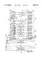
- FIG. 1ais a diagram of a VCSEL having a current confining implant or diffusion below the active region.
- FIG. 1bshows a current confining implant or diffusion above the active region in the VCSEL.
- FIG. 2ais a diagram of another VCSEL, having a current confining implant or diffusion below the active region, that can be integrated with other electronic circuits.
- FIG. 2bshows the VCSEL of FIG. 2a but with the current confining implant or diffusion above the active region.
- FIG. 1aillustrates configuration 10 of the structure.
- alternating epitaxial layers 14 and 16 for laser 10are deposited on a substrate 12 which is doped n- type.
- a broad area contact 15i.e., n- ohmic.
- a bottom mirror 17, consisting of 26 periods of alternating layers of AlAs 16 and Al x Ga.sub.(1-x) As (x0.15 is preferred, but x may have any value greater than 0.05) 14, all doped n- type, are grown to form a highly reflecting mirror 17.
- the total number of mirror periodsmay be greater or less than 26, depending on other parameters.
- a p- type or electrically insulating dopant 20is implanted or diffused in top layers 16 and 14 in order to block current flow on the perimeter of mirror 17, and confine the current to dimension 40.
- This p- or insulating dopantmay be located between 0 and 10 periods (20 layers) below the first confining layers, but preferably is 2 periods below the first confining layer. It is preferable for the depth of implant 20 to be several tenths of a micron but may range between 0.1 and 2 microns.
- Dimension 40may be between 0.1 and 60 microns, but is typically several microns, i.e., 2 to 5 microns.
- xmay be 0.25 or greater. These layers 24 are most likely to be lightly doped, n-type on the layer nearest the n-doped mirror, and p-type on the layer nearest the p-type mirror, although there is a possibility that these could be left undoped.
- the number of GaAs quantum wellsmay be from one to five. Alternatively, one could potentially have an active region 22 without quantum wells, e.g., a region having an emitting number of about 0.2 micron thick.
- a GaAs contact layer 34is formed on top of mirror 30.
- a proton isolation implant 38is placed at the perimeter of contact layer 34, mirror 30, active region 22 and confining layers 24, to separate one device 10 from a like neighboring device on a chip. If a single laser chip 10 were to be made, then it is possible that one could eliminate this proton implant 38, if the implant or diffusion made on top of the n-mirror were to extend all the way to the edge of the chip.
- Laser 10 connectionsare formed by depositing at least one p- type ohmic contact 36 on the top surface of contact layer 34, and a broad area n- type ohmic contact 15 on the back side of wafer substrate 12. The resulting device 10 emits laser light in the range of 760 to 870 nanometers (nm).
- FIG. 1bshows the same VCSEL structure as FIG. 1a, except that dopant 20 is implanted or diffused as an n- type or electrically insulating dopant in layers 31 and 32 of mirror 30, preferably several layers above confining layer 24, to function in blocking current flow from the perimeter of active region 22 and lower mirror 17, and to confine the current flow within dimension 40.
- Dopant 20has similar dimensions as implant or diffusion 20 of FIG. 1a.
- FIG. 2aillustrates configuration 50 of the structure wherein both contacts of the p-n junction can be made from a top surface thereby permitting integration with electronic circuits or other devices on a semi-insulating substrate.
- epitaxial layers 14 and 16 for laser 50are deposited on a semi-insulating substrate 12.
- Layers 16 and 14are grown to form a highly reflecting mirror 17.
- a contact layer 54 of n- doped Al x Ga.sub.(1-x) As (x0.10 but could range from 0.0 to 0.20) is formed on the top layer 16 of mirror 17.
- a p- type or electrically insulating dopant 20is implanted or diffused in order to block current flow on the perimeter of mirror 17 and confine current flow to dimension 40.
- Dopant 20has similar dimensions as implant 20 of FIG. 1a. Unlike the description for FIG. 1a, in this case, the p-type or electrically insulating dopant region cannot extend all the way to the edge of the chip, because it would then prevent us from making this n-ohmic contact 52.
- the p-type or electrically insulating implant or diffused area 20looks like a ring. Dimension 40 is typically between two and five microns.
- the top and mid-portions of structure 50form a mesa on contact layer 54, after etching.
- a p+ GaAs contact layer 34is formed on top of mirror 30.
- Layers 34, 31, 32, 26, 28 and 24are etched on their perimeters down to the contact layer to form a mesa on layer 54.
- Proton isolation implant 38may be inserted at the perimeter of contact layer 34, mirror 30, active region 22, and confining layers 24 of the mesa to isolate current from the edge of the mesa.
- the proton isolation implantmay extend into a portion of contact layer 54 at a depth which is less than the thickness of layer 54.
- the distance between the inside edges of proton implantis between 10 and 100 microns.
- Laser 50 connections for the p-n junctionare formed by depositing at least one p- type ohmic contact 36 on the top surface of contact layer 34, and at least one n- type ohmic contact 52 on an external surface of contact layer 54 outside the perimeter of the mesa incorporating active region 22 and mirror 30, and also outside the perimeter of the p-type or electrically insulating implant or diffusion.
- FIG. 2bshows the same VCSEL structure with similar dimensions and materials as FIG. 1a, except that the dopant 20 is implanted or diffused as an n- type or electrically insulating dopant in layers 31 and 32 of mirror 30, preferably several layers (0 to 10 periods, or 0 to 20 layers) above confining layer 24, to function in blocking current flow from the perimeter of active region 22 and lower mirror 17, and confining the current flow within dimension 40.
- the dopant 20is implanted or diffused as an n- type or electrically insulating dopant in layers 31 and 32 of mirror 30, preferably several layers (0 to 10 periods, or 0 to 20 layers) above confining layer 24, to function in blocking current flow from the perimeter of active region 22 and lower mirror 17, and confining the current flow within dimension 40.
- Device 10, 50can be fabricated by epitaxially depositing an n- type mirror in an OMVPE (Organo-Metallic Vapor Phase Epitaxy) or MBE (Molecular Beam Epitaxy) reactor.
- OMVPEOrganic-Metallic Vapor Phase Epitaxy
- MBEMolecular Beam Epitaxy
- the layers of device 10, 50are removed from the reactor forming the layers, and photoresist is spun onto wafer 10, 50 and patterned in such a way as to protect the layers at an area for a center 40 of device 10, 50.
- the p-, n-, or electrically insulating type dopantis implanted or diffused in a ring outside the protected area having diameter 40.
- Device 10, 50is placed back in the epitaxial growth reactor, and the remaining layers of the structure are deposited.
- the proton isolation implant 38, and n- and p- ohmic contact 15 and 36 depositions, respectively,are made using normal semiconductor processing techniques.
- device 10, 50is operated by applying a forward bias to the p-i-n junction formed by the top p- doped mirror 30, undoped, or lightly doped active region 22, and bottom n- doped mirror 17, the current is forced to flow only through unimplanted center 40 of device 10, 50.
- the depth of the p- n-, or electrically insulating type implant or diffusionneed only be a few tenths of a micron but may range from 0.1 to 2 microns. Therefore, the diameter 40 of the unimplanted or non-diffused region can be kept small to several microns, but may range from 0.1 to 60 microns, with the realization of needing only a very low current to reach lasing threshold, in the cases when this dimension is kept to just a few microns. In addition, the damage due to implant 20 is kept away from the active region 22 of laser 10 and 50, and thus increases device reliability.
- This inventionprovides advantages over the structure disclosed in the above-noted U.S. Pat. No. 5,256,596. Since the epitaxial growth is carried out in two steps, with confining implant or diffusion 20 performed after the first growth, one need only implant or diffuse a few tenths of a micron. In the case of an implant, this limits the energies required, again allowing tighter control of dimensions, and eliminating the need for a mesa etch before the implant. That mesa etch exposes the very reactive AlAs layers 31 in top mirror 30, which would affect reliability. The lower implant 20 energies limit implant damage and magnitude of the implant straggle. In addition, by keeping implant 20 several periods above or below the active region 22, it keeps the reliability limiting implant away from the active layers of the laser.
- Other configurations of the devicewould include the growth of a p- type mirror 17 first, with an n- type or electrically insulating implant or diffusion 20, followed by the active region 22 and an n- type mirror 30.
- InGaAs quantum wells 28can be used for emission in the range of 870-1000 nm. In that case, light can be emitted from either the top or bottom surface of laser 10 or 50.
- Other materialscan be used, such as the AlGaInP material system which results in a laser 10 or 50 emitting in the range 630-700 nm, or the InGaAsP material system for a device 10 or 50 emitting near 1.3 microns.
- compositions mentioned in the descriptions abovecan be varied, i.e., "x" compositions in the mirror might vary from 0.05 to 0.3, or the confining layer "x" compositions might vary from 0.4 to 0.8 at the mirrors and from 0.1 to 0.5 between the quantum wells.
Landscapes
- Physics & Mathematics (AREA)
- Optics & Photonics (AREA)
- Chemical & Material Sciences (AREA)
- Engineering & Computer Science (AREA)
- Nanotechnology (AREA)
- Life Sciences & Earth Sciences (AREA)
- Biophysics (AREA)
- Crystallography & Structural Chemistry (AREA)
- Condensed Matter Physics & Semiconductors (AREA)
- General Physics & Mathematics (AREA)
- Electromagnetism (AREA)
- Semiconductor Lasers (AREA)
Abstract
Description
Claims (18)
Priority Applications (1)
| Application Number | Priority Date | Filing Date | Title |
|---|---|---|---|
| US08/843,116US5893722A (en) | 1996-06-28 | 1997-04-28 | Fabrication of vertical cavity surface emitting laser with current confinement |
Applications Claiming Priority (2)
| Application Number | Priority Date | Filing Date | Title |
|---|---|---|---|
| US08/671,995US5764674A (en) | 1996-06-28 | 1996-06-28 | Current confinement for a vertical cavity surface emitting laser |
| US08/843,116US5893722A (en) | 1996-06-28 | 1997-04-28 | Fabrication of vertical cavity surface emitting laser with current confinement |
Related Parent Applications (1)
| Application Number | Title | Priority Date | Filing Date |
|---|---|---|---|
| US08/671,995DivisionUS5764674A (en) | 1996-06-28 | 1996-06-28 | Current confinement for a vertical cavity surface emitting laser |
Publications (1)
| Publication Number | Publication Date |
|---|---|
| US5893722Atrue US5893722A (en) | 1999-04-13 |
Family
ID=24696720
Family Applications (2)
| Application Number | Title | Priority Date | Filing Date |
|---|---|---|---|
| US08/671,995Expired - LifetimeUS5764674A (en) | 1996-06-28 | 1996-06-28 | Current confinement for a vertical cavity surface emitting laser |
| US08/843,116Expired - LifetimeUS5893722A (en) | 1996-06-28 | 1997-04-28 | Fabrication of vertical cavity surface emitting laser with current confinement |
Family Applications Before (1)
| Application Number | Title | Priority Date | Filing Date |
|---|---|---|---|
| US08/671,995Expired - LifetimeUS5764674A (en) | 1996-06-28 | 1996-06-28 | Current confinement for a vertical cavity surface emitting laser |
Country Status (6)
| Country | Link |
|---|---|
| US (2) | US5764674A (en) |
| EP (2) | EP0907994B1 (en) |
| JP (1) | JP2000514244A (en) |
| CA (1) | CA2257888C (en) |
| DE (2) | DE69726322T2 (en) |
| WO (1) | WO1998000895A1 (en) |
Cited By (62)
| Publication number | Priority date | Publication date | Assignee | Title |
|---|---|---|---|---|
| US5998232A (en)* | 1998-01-16 | 1999-12-07 | Implant Sciences Corporation | Planar technology for producing light-emitting devices |
| US6064683A (en)* | 1997-12-12 | 2000-05-16 | Honeywell Inc. | Bandgap isolated light emitter |
| US6256333B1 (en)* | 1997-12-12 | 2001-07-03 | Honeywell Inc. | VCSEL structure insensitive to mobile hydrogen |
| US6382228B1 (en) | 2000-08-02 | 2002-05-07 | Honeywell International Inc. | Fluid driving system for flow cytometry |
| US6515305B2 (en) | 2000-09-18 | 2003-02-04 | Regents Of The University Of Minnesota | Vertical cavity surface emitting laser with single mode confinement |
| US20030058445A1 (en)* | 2000-08-02 | 2003-03-27 | Fritz Bernard S. | Optical alignment detection system |
| US6542527B1 (en) | 1998-08-27 | 2003-04-01 | Regents Of The University Of Minnesota | Vertical cavity surface emitting laser |
| US6549275B1 (en) | 2000-08-02 | 2003-04-15 | Honeywell International Inc. | Optical detection system for flow cytometry |
| US20030123512A1 (en)* | 2001-12-28 | 2003-07-03 | Johnson Ralph H. | Current confinement,capacitance reduction and isolation of VCSELs using deep elemental traps |
| US6597438B1 (en) | 2000-08-02 | 2003-07-22 | Honeywell International Inc. | Portable flow cytometry |
| US20030142291A1 (en)* | 2000-08-02 | 2003-07-31 | Aravind Padmanabhan | Portable scattering and fluorescence cytometer |
| US6693933B2 (en)* | 2001-03-15 | 2004-02-17 | Honeywell International Inc. | Vertical cavity master oscillator power amplifier |
| US20040032892A1 (en)* | 2001-02-08 | 2004-02-19 | Jurgen Muller | Semiconductor laser |
| US6700130B2 (en) | 2001-06-29 | 2004-03-02 | Honeywell International Inc. | Optical detection system for flow cytometry |
| US6717974B2 (en)* | 2002-04-01 | 2004-04-06 | Lumei Optoelectronics Corporation | Apparatus and method for improving electrical conduction structure of a vertical cavity surface emitting laser |
| US6724798B2 (en) | 2001-12-31 | 2004-04-20 | Honeywell International Inc. | Optoelectronic devices and method of production |
| US20040092055A1 (en)* | 2002-11-11 | 2004-05-13 | Honeywell International Inc., | High speed otpical transceiver package using heterogeneous integration |
| US20040145725A1 (en)* | 2001-06-29 | 2004-07-29 | Fritz Bernard S. | Optical detection system for flow cytometry |
| US20040211077A1 (en)* | 2002-08-21 | 2004-10-28 | Honeywell International Inc. | Method and apparatus for receiving a removable media member |
| US6844537B2 (en) | 2001-12-31 | 2005-01-18 | Honeywell International Inc. | Method and device for measuring the velocity of a moving surface |
| US20050106739A1 (en)* | 2000-08-02 | 2005-05-19 | Cleopatra Cabuz | Miniaturized flow controller with closed loop regulation |
| US20050105077A1 (en)* | 2000-08-02 | 2005-05-19 | Aravind Padmanabhan | Miniaturized cytometer for detecting multiple species in a sample |
| US20050118723A1 (en)* | 2000-08-02 | 2005-06-02 | Aravind Padmanabhan | Optical detection system with polarizing beamsplitter |
| US20050134850A1 (en)* | 2000-08-02 | 2005-06-23 | Tom Rezachek | Optical alignment system for flow cytometry |
| US20050243304A1 (en)* | 2000-08-02 | 2005-11-03 | Honeywell International Inc. | Cytometer analysis cartridge optical configuration |
| US6964496B2 (en) | 2002-07-31 | 2005-11-15 | Benq Corporation | Lamp module and back light device having the same |
| US20050255001A1 (en)* | 2004-05-14 | 2005-11-17 | Honeywell International Inc. | Portable sample analyzer with removable cartridge |
| US20050255600A1 (en)* | 2004-05-14 | 2005-11-17 | Honeywell International Inc. | Portable sample analyzer cartridge |
| US20060023207A1 (en)* | 2004-07-27 | 2006-02-02 | Cox James A | Cytometer having fluid core stream position control |
| US20060046300A1 (en)* | 2004-09-02 | 2006-03-02 | Aravind Padmanabhan | Method and apparatus for determining one or more operating parameters for a microfluidic circuit |
| US20060051096A1 (en)* | 2004-09-01 | 2006-03-09 | Cox James A | Frequency-multiplexed detection of multiple wavelength light for flow cytometry |
| US7016022B2 (en) | 2000-08-02 | 2006-03-21 | Honeywell International Inc. | Dual use detectors for flow cytometry |
| US20060066852A1 (en)* | 2004-09-27 | 2006-03-30 | Fritz Bernard S | Data frame selection for cytometer analysis |
| US20060066840A1 (en)* | 2002-08-21 | 2006-03-30 | Fritz Bernard S | Cytometer having telecentric optics |
| US7026178B2 (en) | 2001-11-13 | 2006-04-11 | Applied Optoelectronics, Inc. | Method for fabricating a VCSEL with ion-implanted current-confinement structure |
| US20060244964A1 (en)* | 2005-04-29 | 2006-11-02 | Honeywell International Inc. | Particle parameter determination system |
| US20060263888A1 (en)* | 2000-06-02 | 2006-11-23 | Honeywell International Inc. | Differential white blood count on a disposable card |
| US20070041013A1 (en)* | 2005-08-16 | 2007-02-22 | Honeywell International Inc. | A light scattering and imaging optical system |
| US20070063140A1 (en)* | 2005-09-22 | 2007-03-22 | Honeywell International Inc. | Optical particulate sensor in oil quality detection |
| US20070166195A1 (en)* | 2004-05-14 | 2007-07-19 | Honeywell International Inc. | Analyzer system |
| US20080195020A1 (en)* | 2000-06-02 | 2008-08-14 | Honeywell International Inc. | A flow control system of a cartridge |
| US20090086249A1 (en)* | 2007-10-01 | 2009-04-02 | Brother Kogyo Kabushiki Kaisha | Image formation device and computer-readable record medium |
| US7553453B2 (en) | 2000-06-02 | 2009-06-30 | Honeywell International Inc. | Assay implementation in a microfluidic format |
| US7630075B2 (en) | 2004-09-27 | 2009-12-08 | Honeywell International Inc. | Circular polarization illumination based analyzer system |
| US20100034704A1 (en)* | 2008-08-06 | 2010-02-11 | Honeywell International Inc. | Microfluidic cartridge channel with reduced bubble formation |
| US8034296B2 (en) | 2005-07-01 | 2011-10-11 | Honeywell International Inc. | Microfluidic card for RBC analysis |
| US8273294B2 (en) | 2005-07-01 | 2012-09-25 | Honeywell International Inc. | Molded cartridge with 3-D hydrodynamic focusing |
| US8323564B2 (en) | 2004-05-14 | 2012-12-04 | Honeywell International Inc. | Portable sample analyzer system |
| US8359484B2 (en) | 2008-09-18 | 2013-01-22 | Honeywell International Inc. | Apparatus and method for operating a computing platform without a battery pack |
| US8361410B2 (en) | 2005-07-01 | 2013-01-29 | Honeywell International Inc. | Flow metered analyzer |
| US8494018B2 (en) | 2009-02-20 | 2013-07-23 | Vixar, Inc. | Direct modulated modified vertical-cavity surface-emitting lasers and method |
| US8663583B2 (en) | 2011-12-27 | 2014-03-04 | Honeywell International Inc. | Disposable cartridge for fluid analysis |
| US8741235B2 (en) | 2011-12-27 | 2014-06-03 | Honeywell International Inc. | Two step sample loading of a fluid analysis cartridge |
| US8741234B2 (en) | 2011-12-27 | 2014-06-03 | Honeywell International Inc. | Disposable cartridge for fluid analysis |
| US8741233B2 (en) | 2011-12-27 | 2014-06-03 | Honeywell International Inc. | Disposable cartridge for fluid analysis |
| US8828320B2 (en) | 2004-05-14 | 2014-09-09 | Honeywell International Inc. | Portable sample analyzer cartridge |
| US8989230B2 (en) | 2009-02-20 | 2015-03-24 | Vixar | Method and apparatus including movable-mirror mems-tuned surface-emitting lasers |
| US9088134B2 (en) | 2011-07-27 | 2015-07-21 | Vixar Inc. | Method and apparatus including improved vertical-cavity surface-emitting lasers |
| US9260693B2 (en) | 2004-12-03 | 2016-02-16 | Cytonome/St, Llc | Actuation of parallel microfluidic arrays |
| US9823252B2 (en) | 2004-12-03 | 2017-11-21 | Cytonome/St, Llc | Unitary cartridge for particle processing |
| US11027278B2 (en) | 2002-04-17 | 2021-06-08 | Cytonome/St, Llc | Methods for controlling fluid flow in a microfluidic system |
| TWI826050B (en)* | 2022-10-19 | 2023-12-11 | 華立捷科技股份有限公司 | Surface emitting laser apparatus and method of manufacturing the same |
Families Citing this family (46)
| Publication number | Priority date | Publication date | Assignee | Title |
|---|---|---|---|---|
| US6055258A (en)* | 1995-11-22 | 2000-04-25 | Polaroid Corporation | Laser diode with an ion-implanted region |
| KR100237188B1 (en)* | 1997-02-10 | 2000-02-01 | 정선종 | Tunable Laser Manufacturing Method |
| JP3745096B2 (en)* | 1997-10-07 | 2006-02-15 | 松下電器産業株式会社 | Surface emitting semiconductor laser and manufacturing method thereof |
| DE69900096T2 (en)* | 1999-02-11 | 2001-08-09 | Avalon Photonics Ltd., Zuerich | Semiconductor laser and manufacturing process |
| US6905900B1 (en)* | 2000-11-28 | 2005-06-14 | Finisar Corporation | Versatile method and system for single mode VCSELs |
| JP2006156776A (en)* | 2004-11-30 | 2006-06-15 | Toshiba Corp | Semiconductor device |
| US8284810B1 (en) | 2008-08-04 | 2012-10-09 | Soraa, Inc. | Solid state laser device using a selected crystal orientation in non-polar or semi-polar GaN containing materials and methods |
| US8247886B1 (en) | 2009-03-09 | 2012-08-21 | Soraa, Inc. | Polarization direction of optical devices using selected spatial configurations |
| US8791499B1 (en)* | 2009-05-27 | 2014-07-29 | Soraa, Inc. | GaN containing optical devices and method with ESD stability |
| US9000466B1 (en) | 2010-08-23 | 2015-04-07 | Soraa, Inc. | Methods and devices for light extraction from a group III-nitride volumetric LED using surface and sidewall roughening |
| US9583678B2 (en) | 2009-09-18 | 2017-02-28 | Soraa, Inc. | High-performance LED fabrication |
| US9293644B2 (en) | 2009-09-18 | 2016-03-22 | Soraa, Inc. | Power light emitting diode and method with uniform current density operation |
| US8933644B2 (en) | 2009-09-18 | 2015-01-13 | Soraa, Inc. | LED lamps with improved quality of light |
| US10147850B1 (en) | 2010-02-03 | 2018-12-04 | Soraa, Inc. | System and method for providing color light sources in proximity to predetermined wavelength conversion structures |
| US8905588B2 (en) | 2010-02-03 | 2014-12-09 | Sorra, Inc. | System and method for providing color light sources in proximity to predetermined wavelength conversion structures |
| US8740413B1 (en) | 2010-02-03 | 2014-06-03 | Soraa, Inc. | System and method for providing color light sources in proximity to predetermined wavelength conversion structures |
| US8313964B2 (en) | 2010-06-18 | 2012-11-20 | Soraa, Inc. | Singulation method and resulting device of thick gallium and nitrogen containing substrates |
| US9450143B2 (en) | 2010-06-18 | 2016-09-20 | Soraa, Inc. | Gallium and nitrogen containing triangular or diamond-shaped configuration for optical devices |
| US8293551B2 (en) | 2010-06-18 | 2012-10-23 | Soraa, Inc. | Gallium and nitrogen containing triangular or diamond-shaped configuration for optical devices |
| US8803452B2 (en) | 2010-10-08 | 2014-08-12 | Soraa, Inc. | High intensity light source |
| US8786053B2 (en) | 2011-01-24 | 2014-07-22 | Soraa, Inc. | Gallium-nitride-on-handle substrate materials and devices and method of manufacture |
| US10036544B1 (en) | 2011-02-11 | 2018-07-31 | Soraa, Inc. | Illumination source with reduced weight |
| US8618742B2 (en)* | 2011-02-11 | 2013-12-31 | Soraa, Inc. | Illumination source and manufacturing methods |
| US8525396B2 (en)* | 2011-02-11 | 2013-09-03 | Soraa, Inc. | Illumination source with direct die placement |
| US8643257B2 (en)* | 2011-02-11 | 2014-02-04 | Soraa, Inc. | Illumination source with reduced inner core size |
| USD694722S1 (en) | 2011-08-15 | 2013-12-03 | Soraa, Inc. | Heatsink |
| US8686431B2 (en) | 2011-08-22 | 2014-04-01 | Soraa, Inc. | Gallium and nitrogen containing trilateral configuration for optical devices |
| US9488324B2 (en) | 2011-09-02 | 2016-11-08 | Soraa, Inc. | Accessories for LED lamp systems |
| US9109760B2 (en) | 2011-09-02 | 2015-08-18 | Soraa, Inc. | Accessories for LED lamps |
| US8884517B1 (en) | 2011-10-17 | 2014-11-11 | Soraa, Inc. | Illumination sources with thermally-isolated electronics |
| US8912025B2 (en) | 2011-11-23 | 2014-12-16 | Soraa, Inc. | Method for manufacture of bright GaN LEDs using a selective removal process |
| JP2015509669A (en) | 2012-03-06 | 2015-03-30 | ソラア インコーポレーテッドSoraa Inc. | Light emitting diode with low refractive index material layer to reduce guided light effect |
| US8985794B1 (en) | 2012-04-17 | 2015-03-24 | Soraa, Inc. | Providing remote blue phosphors in an LED lamp |
| US9360190B1 (en) | 2012-05-14 | 2016-06-07 | Soraa, Inc. | Compact lens for high intensity light source |
| US10436422B1 (en) | 2012-05-14 | 2019-10-08 | Soraa, Inc. | Multi-function active accessories for LED lamps |
| US9995439B1 (en) | 2012-05-14 | 2018-06-12 | Soraa, Inc. | Glare reduced compact lens for high intensity light source |
| US9310052B1 (en) | 2012-09-28 | 2016-04-12 | Soraa, Inc. | Compact lens for high intensity light source |
| US9978904B2 (en) | 2012-10-16 | 2018-05-22 | Soraa, Inc. | Indium gallium nitride light emitting devices |
| US8802471B1 (en) | 2012-12-21 | 2014-08-12 | Soraa, Inc. | Contacts for an n-type gallium and nitrogen substrate for optical devices |
| US8994033B2 (en) | 2013-07-09 | 2015-03-31 | Soraa, Inc. | Contacts for an n-type gallium and nitrogen substrate for optical devices |
| US9419189B1 (en) | 2013-11-04 | 2016-08-16 | Soraa, Inc. | Small LED source with high brightness and high efficiency |
| EP3520183B1 (en)* | 2016-09-28 | 2023-03-01 | Finisar Corporation | Implant regrowth vcsel and vcsel array with heterogeneous combination of different vcsel types |
| WO2018096850A1 (en)* | 2016-11-24 | 2018-05-31 | ソニー株式会社 | Surface emitting laser and electronic device |
| DE102018003982A1 (en)* | 2018-05-17 | 2019-11-21 | 3-5 Power Electronics GmbH | Semiconductor device manufacturing method and semiconductor device |
| CN113659434B (en)* | 2021-06-24 | 2023-03-10 | 威科赛乐微电子股份有限公司 | Manufacturing method of VCSEL chip without Mesa |
| CN115799987B (en)* | 2022-12-02 | 2025-09-05 | 中科纳米张家港化合物半导体研究所 | Vertical cavity surface emitting laser and manufacturing method thereof |
Citations (3)
| Publication number | Priority date | Publication date | Assignee | Title |
|---|---|---|---|---|
| US5115442A (en)* | 1990-04-13 | 1992-05-19 | At&T Bell Laboratories | Top-emitting surface emitting laser structures |
| US5256596A (en)* | 1992-03-26 | 1993-10-26 | Motorola, Inc. | Top emitting VCSEL with implant |
| US5316968A (en)* | 1992-03-25 | 1994-05-31 | At&T Bell Laboratories | Method of making semiconductor surface emitting laser |
Family Cites Families (8)
| Publication number | Priority date | Publication date | Assignee | Title |
|---|---|---|---|---|
| JPS61183986A (en)* | 1985-02-08 | 1986-08-16 | Toshiba Corp | Method for manufacturing semiconductor light emitting device |
| US5160492A (en)* | 1989-04-24 | 1992-11-03 | Hewlett-Packard Company | Buried isolation using ion implantation and subsequent epitaxial growth |
| US5056098A (en)* | 1990-07-05 | 1991-10-08 | At&T Bell Laboratories | Vertical cavity laser with mirror having controllable reflectivity |
| US5245622A (en)* | 1992-05-07 | 1993-09-14 | Bandgap Technology Corporation | Vertical-cavity surface-emitting lasers with intra-cavity structures |
| US5343487A (en)* | 1992-10-01 | 1994-08-30 | Optical Concepts, Inc. | Electrical pumping scheme for vertical-cavity surface-emitting lasers |
| US5337327A (en)* | 1993-02-22 | 1994-08-09 | Motorola, Inc. | VCSEL with lateral index guide |
| US5475701A (en)* | 1993-12-29 | 1995-12-12 | Honeywell Inc. | Integrated laser power monitor |
| US5493577A (en)* | 1994-12-21 | 1996-02-20 | Sandia Corporation | Efficient semiconductor light-emitting device and method |
- 1996
- 1996-06-28USUS08/671,995patent/US5764674A/ennot_activeExpired - Lifetime
- 1997
- 1997-04-28USUS08/843,116patent/US5893722A/ennot_activeExpired - Lifetime
- 1997-06-23DEDE69726322Tpatent/DE69726322T2/ennot_activeExpired - Fee Related
- 1997-06-23CACA002257888Apatent/CA2257888C/ennot_activeExpired - Fee Related
- 1997-06-23EPEP97932241Apatent/EP0907994B1/ennot_activeExpired - Lifetime
- 1997-06-23WOPCT/US1997/010825patent/WO1998000895A1/enactiveIP Right Grant
- 1997-06-23DEDE69711878Tpatent/DE69711878T2/ennot_activeExpired - Fee Related
- 1997-06-23EPEP01203522Apatent/EP1176680B1/ennot_activeExpired - Lifetime
- 1997-06-23JPJP10504222Apatent/JP2000514244A/ennot_activeCeased
Patent Citations (3)
| Publication number | Priority date | Publication date | Assignee | Title |
|---|---|---|---|---|
| US5115442A (en)* | 1990-04-13 | 1992-05-19 | At&T Bell Laboratories | Top-emitting surface emitting laser structures |
| US5316968A (en)* | 1992-03-25 | 1994-05-31 | At&T Bell Laboratories | Method of making semiconductor surface emitting laser |
| US5256596A (en)* | 1992-03-26 | 1993-10-26 | Motorola, Inc. | Top emitting VCSEL with implant |
Cited By (112)
| Publication number | Priority date | Publication date | Assignee | Title |
|---|---|---|---|---|
| US7023896B2 (en) | 1997-12-12 | 2006-04-04 | Finisar Corporation | VCSEL structure insensitive to mobile hydrogen |
| US6064683A (en)* | 1997-12-12 | 2000-05-16 | Honeywell Inc. | Bandgap isolated light emitter |
| US6256333B1 (en)* | 1997-12-12 | 2001-07-03 | Honeywell Inc. | VCSEL structure insensitive to mobile hydrogen |
| US6459719B1 (en) | 1997-12-12 | 2002-10-01 | Honeywell Inc | VCSEL structure insensitive to mobile hydrogen |
| US6522680B1 (en) | 1997-12-12 | 2003-02-18 | Honeywell Inc. | VCSEL structure insensitive to mobile hydrogen |
| US5998232A (en)* | 1998-01-16 | 1999-12-07 | Implant Sciences Corporation | Planar technology for producing light-emitting devices |
| US6542527B1 (en) | 1998-08-27 | 2003-04-01 | Regents Of The University Of Minnesota | Vertical cavity surface emitting laser |
| US20080195020A1 (en)* | 2000-06-02 | 2008-08-14 | Honeywell International Inc. | A flow control system of a cartridge |
| US7420659B1 (en) | 2000-06-02 | 2008-09-02 | Honeywell Interantional Inc. | Flow control system of a cartridge |
| US20060263888A1 (en)* | 2000-06-02 | 2006-11-23 | Honeywell International Inc. | Differential white blood count on a disposable card |
| US7553453B2 (en) | 2000-06-02 | 2009-06-30 | Honeywell International Inc. | Assay implementation in a microfluidic format |
| US7061595B2 (en) | 2000-08-02 | 2006-06-13 | Honeywell International Inc. | Miniaturized flow controller with closed loop regulation |
| US6549275B1 (en) | 2000-08-02 | 2003-04-15 | Honeywell International Inc. | Optical detection system for flow cytometry |
| US7277166B2 (en) | 2000-08-02 | 2007-10-02 | Honeywell International Inc. | Cytometer analysis cartridge optical configuration |
| US6382228B1 (en) | 2000-08-02 | 2002-05-07 | Honeywell International Inc. | Fluid driving system for flow cytometry |
| US7215425B2 (en) | 2000-08-02 | 2007-05-08 | Honeywell International Inc. | Optical alignment for flow cytometry |
| US20030058445A1 (en)* | 2000-08-02 | 2003-03-27 | Fritz Bernard S. | Optical alignment detection system |
| US7471394B2 (en) | 2000-08-02 | 2008-12-30 | Honeywell International Inc. | Optical detection system with polarizing beamsplitter |
| US20030142291A1 (en)* | 2000-08-02 | 2003-07-31 | Aravind Padmanabhan | Portable scattering and fluorescence cytometer |
| US20060256336A1 (en)* | 2000-08-02 | 2006-11-16 | Fritz Bernard S | Optical alignment detection system |
| US7312870B2 (en) | 2000-08-02 | 2007-12-25 | Honeywell International Inc. | Optical alignment detection system |
| US6597438B1 (en) | 2000-08-02 | 2003-07-22 | Honeywell International Inc. | Portable flow cytometry |
| US7630063B2 (en) | 2000-08-02 | 2009-12-08 | Honeywell International Inc. | Miniaturized cytometer for detecting multiple species in a sample |
| US7016022B2 (en) | 2000-08-02 | 2006-03-21 | Honeywell International Inc. | Dual use detectors for flow cytometry |
| US20100014068A1 (en)* | 2000-08-02 | 2010-01-21 | Honeywell International Inc. | Miniaturized cytometer for detecting multiple species in a sample |
| US20050106739A1 (en)* | 2000-08-02 | 2005-05-19 | Cleopatra Cabuz | Miniaturized flow controller with closed loop regulation |
| US20050105077A1 (en)* | 2000-08-02 | 2005-05-19 | Aravind Padmanabhan | Miniaturized cytometer for detecting multiple species in a sample |
| US20050118723A1 (en)* | 2000-08-02 | 2005-06-02 | Aravind Padmanabhan | Optical detection system with polarizing beamsplitter |
| US20050122522A1 (en)* | 2000-08-02 | 2005-06-09 | Aravind Padmanabhan | Optical detection system for flow cytometry |
| US20050134850A1 (en)* | 2000-08-02 | 2005-06-23 | Tom Rezachek | Optical alignment system for flow cytometry |
| US7671987B2 (en) | 2000-08-02 | 2010-03-02 | Honeywell International Inc | Optical detection system for flow cytometry |
| US20050243304A1 (en)* | 2000-08-02 | 2005-11-03 | Honeywell International Inc. | Cytometer analysis cartridge optical configuration |
| US7911617B2 (en) | 2000-08-02 | 2011-03-22 | Honeywell International Inc. | Miniaturized cytometer for detecting multiple species in a sample |
| US6970245B2 (en) | 2000-08-02 | 2005-11-29 | Honeywell International Inc. | Optical alignment detection system |
| US7978329B2 (en) | 2000-08-02 | 2011-07-12 | Honeywell International Inc. | Portable scattering and fluorescence cytometer |
| US6515305B2 (en) | 2000-09-18 | 2003-02-04 | Regents Of The University Of Minnesota | Vertical cavity surface emitting laser with single mode confinement |
| US20040032892A1 (en)* | 2001-02-08 | 2004-02-19 | Jurgen Muller | Semiconductor laser |
| US7177339B2 (en)* | 2001-02-08 | 2007-02-13 | Osram Opto Semiconductors Gmbh | Semiconductor laser |
| US6693933B2 (en)* | 2001-03-15 | 2004-02-17 | Honeywell International Inc. | Vertical cavity master oscillator power amplifier |
| US20040145725A1 (en)* | 2001-06-29 | 2004-07-29 | Fritz Bernard S. | Optical detection system for flow cytometry |
| US7262838B2 (en) | 2001-06-29 | 2007-08-28 | Honeywell International Inc. | Optical detection system for flow cytometry |
| US20070188737A1 (en)* | 2001-06-29 | 2007-08-16 | Honeywell International Inc. | Optical detection system for flow cytometry |
| US7486387B2 (en) | 2001-06-29 | 2009-02-03 | Honeywell International Inc. | Optical detection system for flow cytometry |
| US6700130B2 (en) | 2001-06-29 | 2004-03-02 | Honeywell International Inc. | Optical detection system for flow cytometry |
| US7026178B2 (en) | 2001-11-13 | 2006-04-11 | Applied Optoelectronics, Inc. | Method for fabricating a VCSEL with ion-implanted current-confinement structure |
| US20030123512A1 (en)* | 2001-12-28 | 2003-07-03 | Johnson Ralph H. | Current confinement,capacitance reduction and isolation of VCSELs using deep elemental traps |
| US6738409B2 (en)* | 2001-12-28 | 2004-05-18 | Honeywell International Inc. | Current confinement, capacitance reduction and isolation of VCSELs using deep elemental traps |
| US20040141536A1 (en)* | 2001-12-31 | 2004-07-22 | Honeywell International Inc. | Optoelectronic devices and methods of production |
| US6844537B2 (en) | 2001-12-31 | 2005-01-18 | Honeywell International Inc. | Method and device for measuring the velocity of a moving surface |
| US7151785B2 (en) | 2001-12-31 | 2006-12-19 | Finisar Corporation | Optoelectronic devices and methods of production |
| US6724798B2 (en) | 2001-12-31 | 2004-04-20 | Honeywell International Inc. | Optoelectronic devices and method of production |
| US6717974B2 (en)* | 2002-04-01 | 2004-04-06 | Lumei Optoelectronics Corporation | Apparatus and method for improving electrical conduction structure of a vertical cavity surface emitting laser |
| US11027278B2 (en) | 2002-04-17 | 2021-06-08 | Cytonome/St, Llc | Methods for controlling fluid flow in a microfluidic system |
| US6964496B2 (en) | 2002-07-31 | 2005-11-15 | Benq Corporation | Lamp module and back light device having the same |
| US20060066840A1 (en)* | 2002-08-21 | 2006-03-30 | Fritz Bernard S | Cytometer having telecentric optics |
| US20040211077A1 (en)* | 2002-08-21 | 2004-10-28 | Honeywell International Inc. | Method and apparatus for receiving a removable media member |
| US7000330B2 (en) | 2002-08-21 | 2006-02-21 | Honeywell International Inc. | Method and apparatus for receiving a removable media member |
| US20070236682A9 (en)* | 2002-08-21 | 2007-10-11 | Fritz Bernard S | Cytometer having telecentric optics |
| US7283223B2 (en) | 2002-08-21 | 2007-10-16 | Honeywell International Inc. | Cytometer having telecentric optics |
| US20040092055A1 (en)* | 2002-11-11 | 2004-05-13 | Honeywell International Inc., | High speed otpical transceiver package using heterogeneous integration |
| US6872983B2 (en) | 2002-11-11 | 2005-03-29 | Finisar Corporation | High speed optical transceiver package using heterogeneous integration |
| US20050169569A1 (en)* | 2002-11-11 | 2005-08-04 | Yue Liu | Methods for fabricating integrated optoelectronic devices |
| US7306959B2 (en) | 2002-11-11 | 2007-12-11 | Finisar Corporation | Methods of fabricating integrated optoelectronic devices |
| US20070166195A1 (en)* | 2004-05-14 | 2007-07-19 | Honeywell International Inc. | Analyzer system |
| US8383043B2 (en) | 2004-05-14 | 2013-02-26 | Honeywell International Inc. | Analyzer system |
| US7641856B2 (en) | 2004-05-14 | 2010-01-05 | Honeywell International Inc. | Portable sample analyzer with removable cartridge |
| US20050255600A1 (en)* | 2004-05-14 | 2005-11-17 | Honeywell International Inc. | Portable sample analyzer cartridge |
| US20050255001A1 (en)* | 2004-05-14 | 2005-11-17 | Honeywell International Inc. | Portable sample analyzer with removable cartridge |
| US8828320B2 (en) | 2004-05-14 | 2014-09-09 | Honeywell International Inc. | Portable sample analyzer cartridge |
| US8540946B2 (en) | 2004-05-14 | 2013-09-24 | Honeywell International Inc. | Portable sample analyzer cartridge |
| US8071051B2 (en) | 2004-05-14 | 2011-12-06 | Honeywell International Inc. | Portable sample analyzer cartridge |
| US8323564B2 (en) | 2004-05-14 | 2012-12-04 | Honeywell International Inc. | Portable sample analyzer system |
| US7760351B2 (en) | 2004-07-27 | 2010-07-20 | Honeywell International Inc. | Cytometer having fluid core stream position control |
| US7242474B2 (en) | 2004-07-27 | 2007-07-10 | Cox James A | Cytometer having fluid core stream position control |
| US20080124805A1 (en)* | 2004-07-27 | 2008-05-29 | Honeywell International Inc. | Cytometer having fluid core stream position control |
| US20060023207A1 (en)* | 2004-07-27 | 2006-02-02 | Cox James A | Cytometer having fluid core stream position control |
| US7612871B2 (en) | 2004-09-01 | 2009-11-03 | Honeywell International Inc | Frequency-multiplexed detection of multiple wavelength light for flow cytometry |
| US20060051096A1 (en)* | 2004-09-01 | 2006-03-09 | Cox James A | Frequency-multiplexed detection of multiple wavelength light for flow cytometry |
| US8329118B2 (en) | 2004-09-02 | 2012-12-11 | Honeywell International Inc. | Method and apparatus for determining one or more operating parameters for a microfluidic circuit |
| US20060046300A1 (en)* | 2004-09-02 | 2006-03-02 | Aravind Padmanabhan | Method and apparatus for determining one or more operating parameters for a microfluidic circuit |
| US7630075B2 (en) | 2004-09-27 | 2009-12-08 | Honeywell International Inc. | Circular polarization illumination based analyzer system |
| US7130046B2 (en) | 2004-09-27 | 2006-10-31 | Honeywell International Inc. | Data frame selection for cytometer analysis |
| US20060066852A1 (en)* | 2004-09-27 | 2006-03-30 | Fritz Bernard S | Data frame selection for cytometer analysis |
| US9260693B2 (en) | 2004-12-03 | 2016-02-16 | Cytonome/St, Llc | Actuation of parallel microfluidic arrays |
| US9823252B2 (en) | 2004-12-03 | 2017-11-21 | Cytonome/St, Llc | Unitary cartridge for particle processing |
| US10222378B2 (en) | 2004-12-03 | 2019-03-05 | Cytonome/St, Llc | Unitary cartridge for particle processing |
| US10794913B2 (en) | 2004-12-03 | 2020-10-06 | Cytonome/St, Llc | Unitary cartridge for particle processing |
| US10994273B2 (en) | 2004-12-03 | 2021-05-04 | Cytonome/St, Llc | Actuation of parallel microfluidic arrays |
| US10065188B2 (en) | 2004-12-03 | 2018-09-04 | Cytonome/St, Llc | Actuation of parallel microfluidic arrays |
| US7688427B2 (en) | 2005-04-29 | 2010-03-30 | Honeywell International Inc. | Particle parameter determination system |
| US20060244964A1 (en)* | 2005-04-29 | 2006-11-02 | Honeywell International Inc. | Particle parameter determination system |
| US8361410B2 (en) | 2005-07-01 | 2013-01-29 | Honeywell International Inc. | Flow metered analyzer |
| US8034296B2 (en) | 2005-07-01 | 2011-10-11 | Honeywell International Inc. | Microfluidic card for RBC analysis |
| US8273294B2 (en) | 2005-07-01 | 2012-09-25 | Honeywell International Inc. | Molded cartridge with 3-D hydrodynamic focusing |
| US7843563B2 (en) | 2005-08-16 | 2010-11-30 | Honeywell International Inc. | Light scattering and imaging optical system |
| US20070041013A1 (en)* | 2005-08-16 | 2007-02-22 | Honeywell International Inc. | A light scattering and imaging optical system |
| US7321117B2 (en) | 2005-09-22 | 2008-01-22 | Honeywell International Inc. | Optical particulate sensor in oil quality detection |
| US20070063140A1 (en)* | 2005-09-22 | 2007-03-22 | Honeywell International Inc. | Optical particulate sensor in oil quality detection |
| US20090086249A1 (en)* | 2007-10-01 | 2009-04-02 | Brother Kogyo Kabushiki Kaisha | Image formation device and computer-readable record medium |
| US20100034704A1 (en)* | 2008-08-06 | 2010-02-11 | Honeywell International Inc. | Microfluidic cartridge channel with reduced bubble formation |
| US8359484B2 (en) | 2008-09-18 | 2013-01-22 | Honeywell International Inc. | Apparatus and method for operating a computing platform without a battery pack |
| US8989230B2 (en) | 2009-02-20 | 2015-03-24 | Vixar | Method and apparatus including movable-mirror mems-tuned surface-emitting lasers |
| US8660161B2 (en) | 2009-02-20 | 2014-02-25 | Vixar, Inc. | Push-pull modulated coupled vertical-cavity surface-emitting lasers and method |
| US8494018B2 (en) | 2009-02-20 | 2013-07-23 | Vixar, Inc. | Direct modulated modified vertical-cavity surface-emitting lasers and method |
| US10014661B2 (en) | 2011-07-27 | 2018-07-03 | Vixar, Llc | Method and apparatus including improved vertical-cavity surface-emitting lasers |
| US9088134B2 (en) | 2011-07-27 | 2015-07-21 | Vixar Inc. | Method and apparatus including improved vertical-cavity surface-emitting lasers |
| US8980635B2 (en) | 2011-12-27 | 2015-03-17 | Honeywell International Inc. | Disposable cartridge for fluid analysis |
| US8741233B2 (en) | 2011-12-27 | 2014-06-03 | Honeywell International Inc. | Disposable cartridge for fluid analysis |
| US8741234B2 (en) | 2011-12-27 | 2014-06-03 | Honeywell International Inc. | Disposable cartridge for fluid analysis |
| US8741235B2 (en) | 2011-12-27 | 2014-06-03 | Honeywell International Inc. | Two step sample loading of a fluid analysis cartridge |
| US8663583B2 (en) | 2011-12-27 | 2014-03-04 | Honeywell International Inc. | Disposable cartridge for fluid analysis |
| TWI826050B (en)* | 2022-10-19 | 2023-12-11 | 華立捷科技股份有限公司 | Surface emitting laser apparatus and method of manufacturing the same |
Also Published As
| Publication number | Publication date |
|---|---|
| CA2257888A1 (en) | 1998-01-08 |
| US5764674A (en) | 1998-06-09 |
| DE69711878D1 (en) | 2002-05-16 |
| DE69726322D1 (en) | 2003-12-24 |
| CA2257888C (en) | 2005-05-24 |
| WO1998000895A1 (en) | 1998-01-08 |
| EP1176680B1 (en) | 2003-11-19 |
| EP0907994A1 (en) | 1999-04-14 |
| EP0907994B1 (en) | 2002-04-10 |
| EP1176680A1 (en) | 2002-01-30 |
| DE69711878T2 (en) | 2002-11-21 |
| JP2000514244A (en) | 2000-10-24 |
| DE69726322T2 (en) | 2004-09-16 |
Similar Documents
| Publication | Publication Date | Title |
|---|---|---|
| US5893722A (en) | Fabrication of vertical cavity surface emitting laser with current confinement | |
| US5892784A (en) | N-drive p-common surface emitting laser fabricated on n+ substrate | |
| US6297068B1 (en) | Method for highly compact vertical cavity surface emitting lasers | |
| US5985683A (en) | Method for producing an aperture comprising an oxidized region and a semiconductor material | |
| US5881085A (en) | Lens comprising at least one oxidized layer and method for forming same | |
| US5164949A (en) | Vertical cavity surface emitting laser with lateral injection | |
| US6990135B2 (en) | Distributed bragg reflector for optoelectronic device | |
| US5995531A (en) | VCSEL having polarization control and method of making same | |
| US5896408A (en) | Near planar native-oxide VCSEL devices and arrays using converging oxide ringlets | |
| US6534331B2 (en) | Method for making a vertical-cavity surface emitting laser with improved current confinement | |
| JPH07507183A (en) | Vertical cavity surface emitting laser with internal cavity structure | |
| US7026178B2 (en) | Method for fabricating a VCSEL with ion-implanted current-confinement structure | |
| JP2003218453A (en) | Optoelectronic devices using tunnel junctions disabled for current regulation | |
| WO2003010860A2 (en) | Vertical-cavity surface emitting laser utilizing a reversed-biased diode | |
| US7110427B2 (en) | Hybrid mirror VCSEL | |
| US5848086A (en) | Electrically confined VCSEL | |
| US7095771B2 (en) | Implant damaged oxide insulating region in vertical cavity surface emitting laser | |
| JPH114038A (en) | Laser light-emitting component provided with injection zone having limited width | |
| US6738409B2 (en) | Current confinement, capacitance reduction and isolation of VCSELs using deep elemental traps | |
| EP1648060B1 (en) | Funnel structure vertical external cavity surface-emitting laser (VECSEL) | |
| US7170916B2 (en) | Selectively etchable heterogeneous composite distributed Bragg reflector | |
| US20250079800A1 (en) | Vertical-cavity surface-emitting laser with a planar surface oxidized grating | |
| US20250174965A1 (en) | Vertical-cavity surface-emitting laser that provides polarization mode control | |
| Choquette et al. | Vertical-cavity surface-emitting lasers fabricated by vacuum integrated processing | |
| EP1564855B1 (en) | Surface emitting laser devices and method of manufacture |
Legal Events
| Date | Code | Title | Description |
|---|---|---|---|
| STCF | Information on status: patent grant | Free format text:PATENTED CASE | |
| FEPP | Fee payment procedure | Free format text:PAYOR NUMBER ASSIGNED (ORIGINAL EVENT CODE: ASPN); ENTITY STATUS OF PATENT OWNER: LARGE ENTITY | |
| FPAY | Fee payment | Year of fee payment:4 | |
| AS | Assignment | Owner name:FINISAR CORPORATION, CALIFORNIA Free format text:ASSIGNMENT OF ASSIGNORS INTEREST;ASSIGNOR:HONEYWELL INTERNATIONAL, INC.;REEL/FRAME:014468/0371 Effective date:20040301 Owner name:FINISAR CORPORATION, CALIFORNIA Free format text:ASSIGNMENT OF ASSIGNORS INTEREST;ASSIGNOR:HONEYWELL INTERNATIONAL, INC.;REEL/FRAME:014468/0407 Effective date:20040301 Owner name:FINISAR CORPORATION, CALIFORNIA Free format text:ASSIGNMENT OF ASSIGNORS INTEREST;ASSIGNOR:HONEYWELL INTERNATIONAL, INC.;REEL/FRAME:014484/0171 Effective date:20040301 | |
| AS | Assignment | Owner name:FINISAR CORPORATION, CALIFORNIA Free format text:ASSIGNMENT OF ASSIGNORS INTEREST;ASSIGNOR:HONEYWELL INTERNATIONAL, INC.;REEL/FRAME:014499/0365 Effective date:20040301 | |
| FPAY | Fee payment | Year of fee payment:8 | |
| FPAY | Fee payment | Year of fee payment:12 | |
| AS | Assignment | Owner name:II-VI DELAWARE, INC., DELAWARE Free format text:ASSIGNMENT OF ASSIGNORS INTEREST;ASSIGNOR:FINISAR CORPORATION;REEL/FRAME:052286/0001 Effective date:20190924 |