US5892264A - High frequency analog transistors, method of fabrication and circuit implementation - Google Patents
High frequency analog transistors, method of fabrication and circuit implementationDownload PDFInfo
- Publication number
- US5892264A US5892264AUS08/786,569US78656997AUS5892264AUS 5892264 AUS5892264 AUS 5892264AUS 78656997 AUS78656997 AUS 78656997AUS 5892264 AUS5892264 AUS 5892264A
- Authority
- US
- United States
- Prior art keywords
- region
- base
- heavily doped
- transistor
- collector
- Prior art date
- Legal status (The legal status is an assumption and is not a legal conclusion. Google has not performed a legal analysis and makes no representation as to the accuracy of the status listed.)
- Expired - Lifetime
Links
Images


Classifications
- H—ELECTRICITY
- H10—SEMICONDUCTOR DEVICES; ELECTRIC SOLID-STATE DEVICES NOT OTHERWISE PROVIDED FOR
- H10D—INORGANIC ELECTRIC SEMICONDUCTOR DEVICES
- H10D84/00—Integrated devices formed in or on semiconductor substrates that comprise only semiconducting layers, e.g. on Si wafers or on GaAs-on-Si wafers
- H10D84/60—Integrated devices formed in or on semiconductor substrates that comprise only semiconducting layers, e.g. on Si wafers or on GaAs-on-Si wafers characterised by the integration of at least one component covered by groups H10D10/00 or H10D18/00, e.g. integration of BJTs
- H10D84/67—Complementary BJTs
- H10D84/673—Vertical complementary BJTs
- H—ELECTRICITY
- H10—SEMICONDUCTOR DEVICES; ELECTRIC SOLID-STATE DEVICES NOT OTHERWISE PROVIDED FOR
- H10D—INORGANIC ELECTRIC SEMICONDUCTOR DEVICES
- H10D84/00—Integrated devices formed in or on semiconductor substrates that comprise only semiconducting layers, e.g. on Si wafers or on GaAs-on-Si wafers
- H10D84/01—Manufacture or treatment
- H10D84/0112—Integrating together multiple components covered by H10D8/00, H10D10/00 or H10D18/00, e.g. integrating multiple BJTs
- H10D84/0119—Integrating together multiple components covered by H10D8/00, H10D10/00 or H10D18/00, e.g. integrating multiple BJTs the components including complementary BJTs
- H—ELECTRICITY
- H10—SEMICONDUCTOR DEVICES; ELECTRIC SOLID-STATE DEVICES NOT OTHERWISE PROVIDED FOR
- H10D—INORGANIC ELECTRIC SEMICONDUCTOR DEVICES
- H10D84/00—Integrated devices formed in or on semiconductor substrates that comprise only semiconducting layers, e.g. on Si wafers or on GaAs-on-Si wafers
- H10D84/01—Manufacture or treatment
- H10D84/02—Manufacture or treatment characterised by using material-based technologies
- H10D84/03—Manufacture or treatment characterised by using material-based technologies using Group IV technology, e.g. silicon technology or silicon-carbide [SiC] technology
- H10D84/038—Manufacture or treatment characterised by using material-based technologies using Group IV technology, e.g. silicon technology or silicon-carbide [SiC] technology using silicon technology, e.g. SiGe
- H—ELECTRICITY
- H10—SEMICONDUCTOR DEVICES; ELECTRIC SOLID-STATE DEVICES NOT OTHERWISE PROVIDED FOR
- H10D—INORGANIC ELECTRIC SEMICONDUCTOR DEVICES
- H10D86/00—Integrated devices formed in or on insulating or conducting substrates, e.g. formed in silicon-on-insulator [SOI] substrates or on stainless steel or glass substrates
- H10D86/01—Manufacture or treatment
- H—ELECTRICITY
- H10—SEMICONDUCTOR DEVICES; ELECTRIC SOLID-STATE DEVICES NOT OTHERWISE PROVIDED FOR
- H10D—INORGANIC ELECTRIC SEMICONDUCTOR DEVICES
- H10D86/00—Integrated devices formed in or on insulating or conducting substrates, e.g. formed in silicon-on-insulator [SOI] substrates or on stainless steel or glass substrates
- H10D86/201—Integrated devices formed in or on insulating or conducting substrates, e.g. formed in silicon-on-insulator [SOI] substrates or on stainless steel or glass substrates the substrates comprising an insulating layer on a semiconductor body, e.g. SOI
Definitions
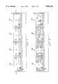
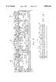
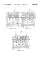
- side wall spacersare formed along the edge of the first level polysilicon adjacent the emitter openings.
- a nitride layeris deposited over the oxide layer 60 and then anisotropically etched to form self-aligned insulative spacers 66 along the sides of all the openings in the polysilicon layer.
- the spacersextend from the first insulative layer 48 to the oxide layer 60.
- Nitrideis the preferred spacer material for reasons discussed below.
- a feature of the processis that the spacer forms a narrower polysilicon opening to define the emitter region, effectively narrowing the emitter dimension. This reduces the emitter-base junction area, thereby increasing the speed of the resulting transistor.
Landscapes
- Bipolar Integrated Circuits (AREA)
Abstract
Description
______________________________________Parameter NPN PNP______________________________________Ft >7.0 GHz >3.0 GHzCurrent Gain >100 >100Early Voltage >60 V >40 V3V.sub.C30 >12 V >12 V3V.sub.C30 >12 V >12 V______________________________________
______________________________________ Parameter NJFET______________________________________ Ft >4.0 GHz Vp >0.5 V BVdss >5.5 V______________________________________
______________________________________Parameter Analog Digital______________________________________Early voltage >40 V >3 VLeakage <100 nA <100 μANoise <100 nv/rt-Hz <1000 nv/rt/Hz______________________________________
______________________________________Parameter Prior Art Present Invention______________________________________Unity Gain Bandwidth 350 MHz 700 MHzSlew Rate 1000 V/μs 2500 V/μsSettling Time (0.1%) 20 ns 6 nsSupply current 40mA 20 mA______________________________________
______________________________________Parameter Prior Art Present Invention______________________________________-3 dB Bandwidth 150 MHz min. 500 MHz minOutput Voltage +/-3 Vpp into 100 ohm +/-3 Vpp into 100 ohmSupply Current 18mA max 24 mA maxSlew Rate 1600 V/μs 2000 V/μs min______________________________________
______________________________________ Prior Voltage CurrentParameter Art Feedback Feedback______________________________________Acquisition Time 500 ns 50 ns 15 nsSlew Rate 90 V/μs 150 V/μs 500 V/μsBandwidth 4.5MHz 45 MHz 200MHzResolution 12bits 12bits 12 bits______________________________________
______________________________________Parameter Prior ArtPresent InventionResolution 12 bit 14 bit 8 bit 11-12 bit______________________________________Settling time to 250 ns 400 ns <10 ns 25 ns1/2 LSB______________________________________
Claims (14)
Priority Applications (1)
| Application Number | Priority Date | Filing Date | Title |
|---|---|---|---|
| US08/786,569US5892264A (en) | 1993-10-04 | 1997-01-21 | High frequency analog transistors, method of fabrication and circuit implementation |
Applications Claiming Priority (2)
| Application Number | Priority Date | Filing Date | Title |
|---|---|---|---|
| US08/131,369US5668397A (en) | 1991-09-27 | 1993-10-04 | High frequency analog transistors, method of fabrication and circuit implementation |
| US08/786,569US5892264A (en) | 1993-10-04 | 1997-01-21 | High frequency analog transistors, method of fabrication and circuit implementation |
Related Parent Applications (1)
| Application Number | Title | Priority Date | Filing Date |
|---|---|---|---|
| US08/131,369DivisionUS5668397A (en) | 1991-09-27 | 1993-10-04 | High frequency analog transistors, method of fabrication and circuit implementation |
Publications (1)
| Publication Number | Publication Date |
|---|---|
| US5892264Atrue US5892264A (en) | 1999-04-06 |
Family
ID=22449153
Family Applications (1)
| Application Number | Title | Priority Date | Filing Date |
|---|---|---|---|
| US08/786,569Expired - LifetimeUS5892264A (en) | 1993-10-04 | 1997-01-21 | High frequency analog transistors, method of fabrication and circuit implementation |
Country Status (1)
| Country | Link |
|---|---|
| US (1) | US5892264A (en) |
Cited By (42)
| Publication number | Priority date | Publication date | Assignee | Title |
|---|---|---|---|---|
| US6140170A (en)* | 1999-08-27 | 2000-10-31 | Lucent Technologies Inc. | Manufacture of complementary MOS and bipolar integrated circuits |
| US6332425B1 (en)* | 1994-11-04 | 2001-12-25 | Hitachi Ltd | Surface treatment method and system |
| US6404020B1 (en)* | 1998-07-31 | 2002-06-11 | Samsung Electronics Co., Ltd. | Method of forming contact pads in a semiconductor device and a semiconductor device formed using the method |
| US20030094673A1 (en)* | 2001-11-16 | 2003-05-22 | International Business Machines Corporation | Semiconductor device and method having multiple subcollectors formed on a common wafer |
| US6586317B1 (en)* | 2001-05-08 | 2003-07-01 | National Semiconductor Corporation | Method of forming a zener diode in a npn and pnp bipolar process flow that requires no additional steps to set the breakdown voltage |
| US20030162360A1 (en)* | 2002-02-25 | 2003-08-28 | Beasom James D. | Reduced mask count buried layer process |
| US6624497B2 (en) | 2002-02-25 | 2003-09-23 | Intersil Americas, Inc | Semiconductor device with a reduced mask count buried layer |
| WO2003036724A3 (en)* | 2001-10-17 | 2003-10-23 | Infineon Technologies Ag | Semiconductor structure with reduced capacitive coupling between components |
| WO2003036723A3 (en)* | 2001-10-17 | 2003-10-23 | Infineon Technologies Ag | Semiconductor structure provided with a component capacitively uncoupled from the substrate |
| US20030205781A1 (en)* | 2000-02-17 | 2003-11-06 | Hamerski Roman J. | Method of manufacturing a device with epitaxial base |
| US6657242B1 (en)* | 1997-03-18 | 2003-12-02 | Telefonaktiebolaget Lm Ericsson (Publ) | Trench-isolated bipolar devices |
| US20040082140A1 (en)* | 2002-10-25 | 2004-04-29 | Jia-Wei Yang | Deep trench isolation structure of a high-voltage device and method for forming thereof |
| US20050104132A1 (en)* | 2001-01-23 | 2005-05-19 | Tsutomu Imoto | Semiconductor device and manufacturing method thereof |
| US20060044719A1 (en)* | 2004-08-30 | 2006-03-02 | Industrial Technology Research | Diode strings and electrostatic discharge protection circuits |
| US20060043489A1 (en)* | 2004-08-30 | 2006-03-02 | Industrial Technology Research Insititute | Diode and applications thereof |
| US20070126080A1 (en)* | 2005-12-05 | 2007-06-07 | International Business Machines Corporation | Bipolar junction transistors (bjts) with second shallow trench isolation (sti) regions, and methods for forming same |
| US20080048287A1 (en)* | 2002-09-29 | 2008-02-28 | Advanced Analogic Technologies, Inc. | Isolation structures for integrated circuits and modular methods of forming the same |
| US20080197446A1 (en)* | 2002-08-14 | 2008-08-21 | Advanced Analogic Technologies, Inc. | Isolated diode |
| US20080197408A1 (en)* | 2002-08-14 | 2008-08-21 | Advanced Analogic Technologies, Inc. | Isolated quasi-vertical DMOS transistor |
| US20080213972A1 (en)* | 2002-08-14 | 2008-09-04 | Advanced Analogic Technologies, Inc. | Processes for forming isolation structures for integrated circuit devices |
| US20080210980A1 (en)* | 2002-08-14 | 2008-09-04 | Advanced Analogic Technologies, Inc. | Isolated CMOS transistors |
| US20080217699A1 (en)* | 2002-08-14 | 2008-09-11 | Advanced Analogic Technologies, Inc. | Isolated Bipolar Transistor |
| US20080217729A1 (en)* | 2002-08-14 | 2008-09-11 | Advanced Analogic Technologies, Inc. | Isolation structures for integrated circuit devices |
| US20080230812A1 (en)* | 2002-08-14 | 2008-09-25 | Advanced Analogic Technologies, Inc. | Isolated junction field-effect transistor |
| US20080237706A1 (en)* | 2007-03-28 | 2008-10-02 | Advanced Analogic Technologies, Inc. | Lateral MOSFET |
| US20080237704A1 (en)* | 2007-03-28 | 2008-10-02 | Advanced Analogic Technologies, Inc. | Isolated trench MOSFET |
| US20080272394A1 (en)* | 2007-05-01 | 2008-11-06 | Ashok Kumar Kapoor | Junction field effect transistors in germanium and silicon-germanium alloys and method for making and using |
| US20100133611A1 (en)* | 2002-08-14 | 2010-06-03 | Advanced Analogic Technologies, Inc. | Isolated transistor |
| US20100253423A1 (en)* | 2007-07-06 | 2010-10-07 | Serge Pontarollo | Diffused integrated resistor |
| US20110101500A1 (en)* | 2009-11-02 | 2011-05-05 | Analog Devices, Inc. | Junction field effect transistor |
| US20110201171A1 (en)* | 2002-08-14 | 2011-08-18 | Advanced Analogic Technologies, Inc. | Processes For Forming Isolation Structures For Integrated Circuit Devices |
| US8285353B2 (en) | 2006-10-11 | 2012-10-09 | Korea Advanced Institute Of Science And Technology | System for analyzing tissue perfusion using concentration of indocyanine green in blood |
| US20130099280A1 (en)* | 2011-10-21 | 2013-04-25 | Analog Devices, Inc. | Overvoltage and/or electrostatic discharge protection device |
| US8742455B2 (en) | 2011-05-11 | 2014-06-03 | Analog Devices, Inc. | Apparatus for electrostatic discharge protection |
| US20150145592A1 (en)* | 2013-11-27 | 2015-05-28 | Qualcomm Incorporated | Dual mode transistor |
| US9202934B2 (en)* | 2013-10-16 | 2015-12-01 | Analog Devices Global | Junction field effect transistor, and method of manufacture thereof |
| US9484739B2 (en) | 2014-09-25 | 2016-11-01 | Analog Devices Global | Overvoltage protection device and method |
| US9520486B2 (en) | 2009-11-04 | 2016-12-13 | Analog Devices, Inc. | Electrostatic protection device |
| US10181719B2 (en) | 2015-03-16 | 2019-01-15 | Analog Devices Global | Overvoltage blocking protection device |
| US10199482B2 (en) | 2010-11-29 | 2019-02-05 | Analog Devices, Inc. | Apparatus for electrostatic discharge protection |
| US20210193847A1 (en)* | 2019-06-24 | 2021-06-24 | Semiconductor Components Industries, Llc | High voltage diode on soi substrate with trench-modified current path |
| US12382684B2 (en) | 2020-09-21 | 2025-08-05 | Texas Instruments Incorporated | Device having multiple emitter layers |
Citations (7)
| Publication number | Priority date | Publication date | Assignee | Title |
|---|---|---|---|---|
| US4471283A (en)* | 1982-11-02 | 1984-09-11 | International Business Machines Corporation | Average current regulation for stepper motors |
| US5072287A (en)* | 1988-02-08 | 1991-12-10 | Kabushiki Kaisha Toshiba | Semiconductor device and method of manufacturing the same |
| US5134403A (en)* | 1990-12-06 | 1992-07-28 | Hewlett-Packard Co. | High speed sampling and digitizing system requiring no hold circuit |
| US5175607A (en)* | 1990-04-26 | 1992-12-29 | Mitsubishi Denki Kabushiki Kaisha | Semiconductor device and manufacturing method thereof |
| US5481129A (en)* | 1991-10-30 | 1996-01-02 | Harris Corporation | Analog-to-digital converter |
| US5606320A (en)* | 1994-12-06 | 1997-02-25 | Pacesetter Inc. | Method and apparatus for micropower analog-to-digital conversion in an implantable medical device |
| US5668397A (en)* | 1991-09-27 | 1997-09-16 | Harris Corp. | High frequency analog transistors, method of fabrication and circuit implementation |
- 1997
- 1997-01-21USUS08/786,569patent/US5892264A/ennot_activeExpired - Lifetime
Patent Citations (7)
| Publication number | Priority date | Publication date | Assignee | Title |
|---|---|---|---|---|
| US4471283A (en)* | 1982-11-02 | 1984-09-11 | International Business Machines Corporation | Average current regulation for stepper motors |
| US5072287A (en)* | 1988-02-08 | 1991-12-10 | Kabushiki Kaisha Toshiba | Semiconductor device and method of manufacturing the same |
| US5175607A (en)* | 1990-04-26 | 1992-12-29 | Mitsubishi Denki Kabushiki Kaisha | Semiconductor device and manufacturing method thereof |
| US5134403A (en)* | 1990-12-06 | 1992-07-28 | Hewlett-Packard Co. | High speed sampling and digitizing system requiring no hold circuit |
| US5668397A (en)* | 1991-09-27 | 1997-09-16 | Harris Corp. | High frequency analog transistors, method of fabrication and circuit implementation |
| US5481129A (en)* | 1991-10-30 | 1996-01-02 | Harris Corporation | Analog-to-digital converter |
| US5606320A (en)* | 1994-12-06 | 1997-02-25 | Pacesetter Inc. | Method and apparatus for micropower analog-to-digital conversion in an implantable medical device |
Cited By (99)
| Publication number | Priority date | Publication date | Assignee | Title |
|---|---|---|---|---|
| US6332425B1 (en)* | 1994-11-04 | 2001-12-25 | Hitachi Ltd | Surface treatment method and system |
| US6657242B1 (en)* | 1997-03-18 | 2003-12-02 | Telefonaktiebolaget Lm Ericsson (Publ) | Trench-isolated bipolar devices |
| US6404020B1 (en)* | 1998-07-31 | 2002-06-11 | Samsung Electronics Co., Ltd. | Method of forming contact pads in a semiconductor device and a semiconductor device formed using the method |
| US6140170A (en)* | 1999-08-27 | 2000-10-31 | Lucent Technologies Inc. | Manufacture of complementary MOS and bipolar integrated circuits |
| US20030205781A1 (en)* | 2000-02-17 | 2003-11-06 | Hamerski Roman J. | Method of manufacturing a device with epitaxial base |
| US6803298B2 (en)* | 2000-02-17 | 2004-10-12 | Fabtech, Inc. | Method of manufacturing a device with epitaxial base |
| US20050104132A1 (en)* | 2001-01-23 | 2005-05-19 | Tsutomu Imoto | Semiconductor device and manufacturing method thereof |
| US6586317B1 (en)* | 2001-05-08 | 2003-07-01 | National Semiconductor Corporation | Method of forming a zener diode in a npn and pnp bipolar process flow that requires no additional steps to set the breakdown voltage |
| WO2003036723A3 (en)* | 2001-10-17 | 2003-10-23 | Infineon Technologies Ag | Semiconductor structure provided with a component capacitively uncoupled from the substrate |
| WO2003036724A3 (en)* | 2001-10-17 | 2003-10-23 | Infineon Technologies Ag | Semiconductor structure with reduced capacitive coupling between components |
| US7064416B2 (en)* | 2001-11-16 | 2006-06-20 | International Business Machines Corporation | Semiconductor device and method having multiple subcollectors formed on a common wafer |
| US20030094673A1 (en)* | 2001-11-16 | 2003-05-22 | International Business Machines Corporation | Semiconductor device and method having multiple subcollectors formed on a common wafer |
| US7303968B2 (en) | 2001-11-16 | 2007-12-04 | International Business Machines Corporation | Semiconductor device and method having multiple subcollectors formed on a common wafer |
| US20060157824A1 (en)* | 2001-11-16 | 2006-07-20 | International Business Machines Corporation | Semiconductor device and method having multiple subcollectors formed on a common wafer |
| US6624497B2 (en) | 2002-02-25 | 2003-09-23 | Intersil Americas, Inc | Semiconductor device with a reduced mask count buried layer |
| USRE41477E1 (en) | 2002-02-25 | 2010-08-10 | Beasom James D | Semiconductor device with a reduced mask count buried layer |
| US20030162360A1 (en)* | 2002-02-25 | 2003-08-28 | Beasom James D. | Reduced mask count buried layer process |
| US6979624B2 (en) | 2002-02-25 | 2005-12-27 | Intersil Americas Inc. | Reduced mask count buried layer process |
| US8659116B2 (en) | 2002-08-14 | 2014-02-25 | Advanced Analogic Technologies Incorporated | Isolated transistor |
| US20080197446A1 (en)* | 2002-08-14 | 2008-08-21 | Advanced Analogic Technologies, Inc. | Isolated diode |
| US7812403B2 (en) | 2002-08-14 | 2010-10-12 | Advanced Analogic Technologies, Inc. | Isolation structures for integrated circuit devices |
| US7902630B2 (en) | 2002-08-14 | 2011-03-08 | Advanced Analogic Technologies, Inc. | Isolated bipolar transistor |
| US7939420B2 (en) | 2002-08-14 | 2011-05-10 | Advanced Analogic Technologies, Inc. | Processes for forming isolation structures for integrated circuit devices |
| US7956391B2 (en)* | 2002-08-14 | 2011-06-07 | Advanced Analogic Technologies, Inc. | Isolated junction field-effect transistor |
| US20110201171A1 (en)* | 2002-08-14 | 2011-08-18 | Advanced Analogic Technologies, Inc. | Processes For Forming Isolation Structures For Integrated Circuit Devices |
| US20100133611A1 (en)* | 2002-08-14 | 2010-06-03 | Advanced Analogic Technologies, Inc. | Isolated transistor |
| US20090236683A1 (en)* | 2002-08-14 | 2009-09-24 | Advanced Analogic Technologies, Inc. | Isolation structures for integrated circuits |
| US8664715B2 (en) | 2002-08-14 | 2014-03-04 | Advanced Analogic Technologies Incorporated | Isolated transistor |
| US20080197408A1 (en)* | 2002-08-14 | 2008-08-21 | Advanced Analogic Technologies, Inc. | Isolated quasi-vertical DMOS transistor |
| US8089129B2 (en) | 2002-08-14 | 2012-01-03 | Advanced Analogic Technologies, Inc. | Isolated CMOS transistors |
| US20080213972A1 (en)* | 2002-08-14 | 2008-09-04 | Advanced Analogic Technologies, Inc. | Processes for forming isolation structures for integrated circuit devices |
| US20080210980A1 (en)* | 2002-08-14 | 2008-09-04 | Advanced Analogic Technologies, Inc. | Isolated CMOS transistors |
| US20080217699A1 (en)* | 2002-08-14 | 2008-09-11 | Advanced Analogic Technologies, Inc. | Isolated Bipolar Transistor |
| US20080217729A1 (en)* | 2002-08-14 | 2008-09-11 | Advanced Analogic Technologies, Inc. | Isolation structures for integrated circuit devices |
| US20080230812A1 (en)* | 2002-08-14 | 2008-09-25 | Advanced Analogic Technologies, Inc. | Isolated junction field-effect transistor |
| US8097522B2 (en) | 2002-08-14 | 2012-01-17 | Advanced Analogic Technologies, Inc. | Modular methods of forming isolation structures for integrated circuits |
| US8513087B2 (en) | 2002-08-14 | 2013-08-20 | Advanced Analogic Technologies, Incorporated | Processes for forming isolation structures for integrated circuit devices |
| US7834421B2 (en) | 2002-08-14 | 2010-11-16 | Advanced Analogic Technologies, Inc. | Isolated diode |
| US9257504B2 (en) | 2002-09-29 | 2016-02-09 | Advanced Analogic Technologies Incorporated | Isolation structures for semiconductor devices |
| US20080048287A1 (en)* | 2002-09-29 | 2008-02-28 | Advanced Analogic Technologies, Inc. | Isolation structures for integrated circuits and modular methods of forming the same |
| US8728904B2 (en) | 2002-09-29 | 2014-05-20 | Advanced Analogic Technologies (Hong Kong) Limited | Method of forming isolation structure in semiconductor substrate |
| US9905640B2 (en) | 2002-09-29 | 2018-02-27 | Skyworks Solutions (Hong Kong) Limited | Isolation structures for semiconductor devices including trenches containing conductive material |
| US10074716B2 (en) | 2002-09-29 | 2018-09-11 | Skyworks Solutions (Hong Kong) Limited | Saucer-shaped isolation structures for semiconductor devices |
| US20060027890A1 (en)* | 2002-10-25 | 2006-02-09 | Vanguard International Semiconductor Corporation | Deep trench isolation structure of a high-voltage device and method for forming thereof |
| US6972471B2 (en)* | 2002-10-25 | 2005-12-06 | Vanguard International Semiconductor Corporation | Deep trench isolation structure of a high-voltage device and method for forming thereof |
| US20040082140A1 (en)* | 2002-10-25 | 2004-04-29 | Jia-Wei Yang | Deep trench isolation structure of a high-voltage device and method for forming thereof |
| US7242070B2 (en) | 2002-10-25 | 2007-07-10 | Vanguard International Semiconductor Corporation | Deep trench isolation structure of a high-voltage device and method for forming thereof |
| US7525779B2 (en) | 2004-08-30 | 2009-04-28 | Zi-Ping Chen | Diode strings and electrostatic discharge protection circuits |
| US7372109B2 (en)* | 2004-08-30 | 2008-05-13 | Zi-Ping Chen | Diode and applications thereof |
| US7696580B2 (en) | 2004-08-30 | 2010-04-13 | Zi-Ping Chen | Diode and applications thereof |
| US20080203424A1 (en)* | 2004-08-30 | 2008-08-28 | Zi-Ping Chen | Diode and applications thereof |
| US20060043489A1 (en)* | 2004-08-30 | 2006-03-02 | Industrial Technology Research Insititute | Diode and applications thereof |
| US20060044719A1 (en)* | 2004-08-30 | 2006-03-02 | Industrial Technology Research | Diode strings and electrostatic discharge protection circuits |
| US7342293B2 (en)* | 2005-12-05 | 2008-03-11 | International Business Machines Corporation | Bipolar junction transistors (BJTS) with second shallow trench isolation (STI) regions, and methods for forming same |
| US20070126080A1 (en)* | 2005-12-05 | 2007-06-07 | International Business Machines Corporation | Bipolar junction transistors (bjts) with second shallow trench isolation (sti) regions, and methods for forming same |
| US7701033B2 (en) | 2006-05-31 | 2010-04-20 | Advanced Analogic Technologies, Inc. | Isolation structures for integrated circuits |
| US7825488B2 (en) | 2006-05-31 | 2010-11-02 | Advanced Analogic Technologies, Inc. | Isolation structures for integrated circuits and modular methods of forming the same |
| US20080290450A1 (en)* | 2006-05-31 | 2008-11-27 | Advanced Analogic Technologies, Inc. | Isolation structures for integrated circuits |
| US7898060B2 (en) | 2006-05-31 | 2011-03-01 | Advanced Analogic Technologies, Inc. | Isolation structures for integrated circuits |
| US20080290449A1 (en)* | 2006-05-31 | 2008-11-27 | Advanced Analogic Technologies, Inc. | Isolation structures for integrated circuits |
| US20080290451A1 (en)* | 2006-05-31 | 2008-11-27 | Advanced Analogic Technologies, Inc. | Isolation structures for integrated circuits |
| US7800198B2 (en) | 2006-05-31 | 2010-09-21 | Advanced Analogic Technologies, Inc. | Isolation structures for integrated circuits |
| US8071462B2 (en) | 2006-05-31 | 2011-12-06 | Advanced Analogic Technologies, Inc. | Isolation structures for integrated circuits and modular methods of forming the same |
| US8285353B2 (en) | 2006-10-11 | 2012-10-09 | Korea Advanced Institute Of Science And Technology | System for analyzing tissue perfusion using concentration of indocyanine green in blood |
| US8030731B2 (en) | 2007-03-28 | 2011-10-04 | Advanced Analogic Technologies, Inc. | Isolated rectifier diode |
| US20080237704A1 (en)* | 2007-03-28 | 2008-10-02 | Advanced Analogic Technologies, Inc. | Isolated trench MOSFET |
| US7737526B2 (en) | 2007-03-28 | 2010-06-15 | Advanced Analogic Technologies, Inc. | Isolated trench MOSFET in epi-less semiconductor sustrate |
| US20080237782A1 (en)* | 2007-03-28 | 2008-10-02 | Advanced Analogic Technologies, Inc. | Isolated rectifier diode |
| US7795681B2 (en) | 2007-03-28 | 2010-09-14 | Advanced Analogic Technologies, Inc. | Isolated lateral MOSFET in epi-less substrate |
| US20080237783A1 (en)* | 2007-03-28 | 2008-10-02 | Advanced Analogic Technologies, Inc. | Isolated bipolar transistor |
| US20080237656A1 (en)* | 2007-03-28 | 2008-10-02 | Advanced Analogic Technologies, Inc. | Isolated junction field-effect transistor |
| US8138570B2 (en) | 2007-03-28 | 2012-03-20 | Advanced Analogic Technologies, Inc. | Isolated junction field-effect transistor |
| US8258575B2 (en) | 2007-03-28 | 2012-09-04 | Advanced Analogic Technologies, Inc. | Isolated drain-centric lateral MOSFET |
| US7868414B2 (en) | 2007-03-28 | 2011-01-11 | Advanced Analogic Technologies, Inc. | Isolated bipolar transistor |
| US20110012196A1 (en)* | 2007-03-28 | 2011-01-20 | Advanced Analogic Technologies, Inc. | Isolated drain-centric lateral MOSFET |
| US20080237706A1 (en)* | 2007-03-28 | 2008-10-02 | Advanced Analogic Technologies, Inc. | Lateral MOSFET |
| US20080272394A1 (en)* | 2007-05-01 | 2008-11-06 | Ashok Kumar Kapoor | Junction field effect transistors in germanium and silicon-germanium alloys and method for making and using |
| US8564096B2 (en)* | 2007-07-06 | 2013-10-22 | Stmicroelectronics Sa | Diffused integrated resistor |
| US20100253423A1 (en)* | 2007-07-06 | 2010-10-07 | Serge Pontarollo | Diffused integrated resistor |
| KR101456408B1 (en)* | 2008-02-27 | 2014-11-04 | 어드밴스드 아날로직 테크놀로지스 인코퍼레이티드 | Isolated transistors and diodes and isolation and termination structures for semiconductor die |
| KR101483404B1 (en)* | 2008-02-27 | 2015-01-15 | 어드밴스드 아날로직 테크놀로지스 인코퍼레이티드 | Isolated transistors and diodes and isolation and termination structures for semiconductor die |
| US8263469B2 (en) | 2009-11-02 | 2012-09-11 | Analog Devices, Inc. | Methods of forming a bipolar transistor |
| US20110101500A1 (en)* | 2009-11-02 | 2011-05-05 | Analog Devices, Inc. | Junction field effect transistor |
| US8058704B2 (en) | 2009-11-02 | 2011-11-15 | Analog Devices, Inc. | Bipolar transistor |
| WO2011053926A3 (en)* | 2009-11-02 | 2011-06-30 | Analog Devices, Inc. | Bipolar transistor |
| US9520486B2 (en) | 2009-11-04 | 2016-12-13 | Analog Devices, Inc. | Electrostatic protection device |
| US10043792B2 (en) | 2009-11-04 | 2018-08-07 | Analog Devices, Inc. | Electrostatic protection device |
| US10199482B2 (en) | 2010-11-29 | 2019-02-05 | Analog Devices, Inc. | Apparatus for electrostatic discharge protection |
| US8742455B2 (en) | 2011-05-11 | 2014-06-03 | Analog Devices, Inc. | Apparatus for electrostatic discharge protection |
| US8816389B2 (en)* | 2011-10-21 | 2014-08-26 | Analog Devices, Inc. | Overvoltage and/or electrostatic discharge protection device |
| US20130099280A1 (en)* | 2011-10-21 | 2013-04-25 | Analog Devices, Inc. | Overvoltage and/or electrostatic discharge protection device |
| US9202934B2 (en)* | 2013-10-16 | 2015-12-01 | Analog Devices Global | Junction field effect transistor, and method of manufacture thereof |
| US9601607B2 (en)* | 2013-11-27 | 2017-03-21 | Qualcomm Incorporated | Dual mode transistor |
| US20150145592A1 (en)* | 2013-11-27 | 2015-05-28 | Qualcomm Incorporated | Dual mode transistor |
| US9484739B2 (en) | 2014-09-25 | 2016-11-01 | Analog Devices Global | Overvoltage protection device and method |
| US10181719B2 (en) | 2015-03-16 | 2019-01-15 | Analog Devices Global | Overvoltage blocking protection device |
| US20210193847A1 (en)* | 2019-06-24 | 2021-06-24 | Semiconductor Components Industries, Llc | High voltage diode on soi substrate with trench-modified current path |
| US12125923B2 (en)* | 2019-06-24 | 2024-10-22 | Semiconductor Components Industries, Llc | High voltage diode on SOI substrate with trench-modified current path |
| US12382684B2 (en) | 2020-09-21 | 2025-08-05 | Texas Instruments Incorporated | Device having multiple emitter layers |
Similar Documents
| Publication | Publication Date | Title |
|---|---|---|
| US5892264A (en) | High frequency analog transistors, method of fabrication and circuit implementation | |
| US5668397A (en) | High frequency analog transistors, method of fabrication and circuit implementation | |
| US5068756A (en) | Integrated circuit composed of group III-V compound field effect and bipolar semiconductors | |
| CA1267444A (en) | Bicmos process having narrow bipolar emitter and implanted aluminum isolation | |
| US5323055A (en) | Semiconductor device with buried conductor and interconnection layer | |
| US5405790A (en) | Method of forming a semiconductor structure having MOS, bipolar, and varactor devices | |
| KR100691036B1 (en) | Integrated circuit comprising lateral bipolar transistor and method of manufacturing the same | |
| CA1238117A (en) | Stud-defined integrated circuit structure and fabrication | |
| JPH0677421A (en) | Transistor manufacturing method | |
| EP0243622B1 (en) | Shallow junction complementary vertical bipolar transistor pair | |
| US4512075A (en) | Method of making an integrated injection logic cell having self-aligned collector and base reduced resistance utilizing selective diffusion from polycrystalline regions | |
| KR0134383B1 (en) | Integrated bipolar & cmos transistor with titarium nitride interconnection | |
| US4735912A (en) | Process of fabricating a semiconductor IC device | |
| US4866000A (en) | Fabrication method for semiconductor integrated circuits | |
| US6767797B2 (en) | Method of fabricating complementary self-aligned bipolar transistors | |
| US6596600B1 (en) | Integrated injection logic semiconductor device and method of fabricating the same | |
| EP1021835B1 (en) | Method of manufacturing a bipolar power transistor | |
| EP0375323A1 (en) | A high-performance vertical PNP transistor compatible with an advanced ECL bipolar technology and method of manufacturing same | |
| US7101750B2 (en) | Semiconductor device for integrated injection logic cell and process for fabricating the same | |
| US4067037A (en) | Transistor having high ft at low currents | |
| KR930010118B1 (en) | Making method of semiconductor device | |
| GB2081508A (en) | Integrated injection logic cell having self-aligned collector and base with reduced base resistance and method of making same | |
| KR100200058B1 (en) | How to separate a reverse infusion | |
| JPS6248388B2 (en) | ||
| EP0710399A1 (en) | Process for fabricating semiconductor devices having arsenic emitters |
Legal Events
| Date | Code | Title | Description |
|---|---|---|---|
| STCF | Information on status: patent grant | Free format text:PATENTED CASE | |
| AS | Assignment | Owner name:INTERSIL CORPORATION, FLORIDA Free format text:ASSIGNMENT OF ASSIGNORS INTEREST;ASSIGNOR:HARRIS CORPORATION;REEL/FRAME:010247/0043 Effective date:19990813 | |
| AS | Assignment | Owner name:CREDIT SUISSE FIRST BOSTON, AS COLLATERAL AGENT, N Free format text:SECURITY INTEREST;ASSIGNOR:INTERSIL CORPORATION;REEL/FRAME:010351/0410 Effective date:19990813 | |
| FEPP | Fee payment procedure | Free format text:PAYOR NUMBER ASSIGNED (ORIGINAL EVENT CODE: ASPN); ENTITY STATUS OF PATENT OWNER: LARGE ENTITY | |
| FPAY | Fee payment | Year of fee payment:4 | |
| REMI | Maintenance fee reminder mailed | ||
| FPAY | Fee payment | Year of fee payment:8 | |
| AS | Assignment | Owner name:INTERSIL AMERICAS, INC., CALIFORNIA Free format text:ASSIGNMENT OF ASSIGNORS INTEREST;ASSIGNOR:INTERSIL COMMUNICATIONS, INC.;REEL/FRAME:019181/0046 Effective date:20070418 Owner name:INTERSIL COMMUNICATIONS, INC., CALIFORNIA Free format text:CHANGE OF NAME;ASSIGNOR:INTERSIL CORPORATION;REEL/FRAME:019181/0031 Effective date:20010523 | |
| AS | Assignment | Owner name:MORGAN STANLEY & CO. INCORPORATED,NEW YORK Free format text:SECURITY AGREEMENT;ASSIGNORS:INTERSIL CORPORATION;TECHWELL, INC.;INTERSIL COMMUNICATIONS, INC.;AND OTHERS;REEL/FRAME:024329/0411 Effective date:20100427 Owner name:MORGAN STANLEY & CO. INCORPORATED, NEW YORK Free format text:SECURITY AGREEMENT;ASSIGNORS:INTERSIL CORPORATION;TECHWELL, INC.;INTERSIL COMMUNICATIONS, INC.;AND OTHERS;REEL/FRAME:024329/0411 Effective date:20100427 | |
| AS | Assignment | Owner name:INTERSIL CORPORATION,FLORIDA Free format text:RELEASE BY SECURED PARTY;ASSIGNOR:CREDIT SUISSE FIRST BOSTON;REEL/FRAME:024445/0049 Effective date:20030306 | |
| FPAY | Fee payment | Year of fee payment:12 |