US5892243A - High-temperature SSNS and SNS Josephson junction and method of making junction - Google Patents
High-temperature SSNS and SNS Josephson junction and method of making junctionDownload PDFInfo
- Publication number
- US5892243A US5892243AUS08/761,412US76141296AUS5892243AUS 5892243 AUS5892243 AUS 5892243AUS 76141296 AUS76141296 AUS 76141296AUS 5892243 AUS5892243 AUS 5892243A
- Authority
- US
- United States
- Prior art keywords
- layer
- superconductive
- junction
- hts
- ramp edge
- Prior art date
- Legal status (The legal status is an assumption and is not a legal conclusion. Google has not performed a legal analysis and makes no representation as to the accuracy of the status listed.)
- Expired - Fee Related
Links
- 238000004519manufacturing processMethods0.000titledescription6
- 230000004888barrier functionEffects0.000claimsabstractdescription51
- 239000000758substrateSubstances0.000claimsabstractdescription36
- 239000002887superconductorSubstances0.000claimsabstract2
- 239000000463materialSubstances0.000claimsdescription46
- 229910021521yttrium barium copper oxideInorganic materials0.000claimsdescription11
- 230000001419dependent effectEffects0.000claimsdescription6
- 229910052779NeodymiumInorganic materials0.000claimsdescription5
- 229910052691ErbiumInorganic materials0.000claimsdescription4
- 229910002244LaAlO3Inorganic materials0.000claimsdescription4
- 229910002370SrTiO3Inorganic materials0.000claimsdescription3
- FWGZLZNGAVBRPW-UHFFFAOYSA-Nalumane;strontiumChemical compound[AlH3].[Sr]FWGZLZNGAVBRPW-UHFFFAOYSA-N0.000claimsdescription3
- LNTHITQWFMADLM-UHFFFAOYSA-Ngallic acidChemical compoundOC(=O)C1=CC(O)=C(O)C(O)=C1LNTHITQWFMADLM-UHFFFAOYSA-N0.000claimsdescription3
- QEFYFXOXNSNQGX-UHFFFAOYSA-Nneodymium atomChemical compound[Nd]QEFYFXOXNSNQGX-UHFFFAOYSA-N0.000claimsdescription3
- 229910052692DysprosiumInorganic materials0.000claimsdescription2
- 229910052688GadoliniumInorganic materials0.000claimsdescription2
- 229910052689HolmiumInorganic materials0.000claimsdescription2
- 229910052765LutetiumInorganic materials0.000claimsdescription2
- 229910052772SamariumInorganic materials0.000claimsdescription2
- 229910052775ThuliumInorganic materials0.000claimsdescription2
- 229910052788bariumInorganic materials0.000claimsdescription2
- 229910052797bismuthInorganic materials0.000claimsdescription2
- 229910052796boronInorganic materials0.000claimsdescription2
- 229910052712strontiumInorganic materials0.000claimsdescription2
- 229910052716thalliumInorganic materials0.000claimsdescription2
- 238000000034methodMethods0.000abstractdescription36
- 229920002120photoresistant polymerPolymers0.000abstractdescription19
- 238000011065in-situ storageMethods0.000abstractdescription9
- 230000000873masking effectEffects0.000abstractdescription6
- 230000015572biosynthetic processEffects0.000abstractdescription3
- 238000000992sputter etchingMethods0.000abstract1
- 230000008569processEffects0.000description21
- 238000000151depositionMethods0.000description11
- 238000011109contaminationMethods0.000description7
- 238000004140cleaningMethods0.000description5
- 230000008021depositionEffects0.000description5
- 150000002500ionsChemical class0.000description5
- 239000000126substanceSubstances0.000description5
- QVGXLLKOCUKJST-UHFFFAOYSA-Natomic oxygenChemical compound[O]QVGXLLKOCUKJST-UHFFFAOYSA-N0.000description4
- 239000010949copperSubstances0.000description4
- 239000003989dielectric materialSubstances0.000description4
- 238000005516engineering processMethods0.000description4
- 238000005530etchingMethods0.000description4
- 239000007943implantSubstances0.000description4
- 239000001301oxygenSubstances0.000description4
- 229910052760oxygenInorganic materials0.000description4
- 238000007736thin film deposition techniqueMethods0.000description4
- 230000003071parasitic effectEffects0.000description3
- 238000005240physical vapour depositionMethods0.000description3
- 238000004544sputter depositionMethods0.000description3
- 239000010409thin filmSubstances0.000description3
- 230000002411adverseEffects0.000description2
- 150000001875compoundsChemical class0.000description2
- 230000008878couplingEffects0.000description2
- 238000010168coupling processMethods0.000description2
- 238000005859coupling reactionMethods0.000description2
- 239000013078crystalSubstances0.000description2
- 238000011066ex-situ storageMethods0.000description2
- 239000010408filmSubstances0.000description2
- 239000007789gasSubstances0.000description2
- 238000009413insulationMethods0.000description2
- -1lanthanum aluminateChemical class0.000description2
- 238000000608laser ablationMethods0.000description2
- 238000001020plasma etchingMethods0.000description2
- VEALVRVVWBQVSL-UHFFFAOYSA-Nstrontium titanateChemical compound[Sr+2].[O-][Ti]([O-])=OVEALVRVVWBQVSL-UHFFFAOYSA-N0.000description2
- 238000000427thin-film depositionMethods0.000description2
- 238000001039wet etchingMethods0.000description2
- MUKYGUZFFPFWQM-UHFFFAOYSA-N[Cu]=O.[Ba].[Pr]Chemical compound[Cu]=O.[Ba].[Pr]MUKYGUZFFPFWQM-UHFFFAOYSA-N0.000description1
- BTGZYWWSOPEHMM-UHFFFAOYSA-N[O].[Cu].[Y].[Ba]Chemical compound[O].[Cu].[Y].[Ba]BTGZYWWSOPEHMM-UHFFFAOYSA-N0.000description1
- 230000001413cellular effectEffects0.000description1
- 238000001816coolingMethods0.000description1
- 230000007123defenseEffects0.000description1
- 238000005137deposition processMethods0.000description1
- 230000001066destructive effectEffects0.000description1
- 238000001514detection methodMethods0.000description1
- 230000001627detrimental effectEffects0.000description1
- 230000000694effectsEffects0.000description1
- 230000036039immunityEffects0.000description1
- 238000005468ion implantationMethods0.000description1
- 229910052746lanthanumInorganic materials0.000description1
- 238000000059patterningMethods0.000description1
- 238000003908quality control methodMethods0.000description1
- 239000004065semiconductorSubstances0.000description1
- 229910052710siliconInorganic materials0.000description1
- 239000010703siliconSubstances0.000description1
- 230000007704transitionEffects0.000description1
- 238000011282treatmentMethods0.000description1
- 230000005641tunnelingEffects0.000description1
Images


Classifications
- H—ELECTRICITY
- H10—SEMICONDUCTOR DEVICES; ELECTRIC SOLID-STATE DEVICES NOT OTHERWISE PROVIDED FOR
- H10N—ELECTRIC SOLID-STATE DEVICES NOT OTHERWISE PROVIDED FOR
- H10N60/00—Superconducting devices
- H10N60/10—Junction-based devices
- H10N60/12—Josephson-effect devices
- H10N60/124—Josephson-effect devices comprising high-Tc ceramic materials
- H—ELECTRICITY
- H10—SEMICONDUCTOR DEVICES; ELECTRIC SOLID-STATE DEVICES NOT OTHERWISE PROVIDED FOR
- H10N—ELECTRIC SOLID-STATE DEVICES NOT OTHERWISE PROVIDED FOR
- H10N60/00—Superconducting devices
- H10N60/01—Manufacture or treatment
- H10N60/0912—Manufacture or treatment of Josephson-effect devices
- H10N60/0941—Manufacture or treatment of Josephson-effect devices comprising high-Tc ceramic materials
- Y—GENERAL TAGGING OF NEW TECHNOLOGICAL DEVELOPMENTS; GENERAL TAGGING OF CROSS-SECTIONAL TECHNOLOGIES SPANNING OVER SEVERAL SECTIONS OF THE IPC; TECHNICAL SUBJECTS COVERED BY FORMER USPC CROSS-REFERENCE ART COLLECTIONS [XRACs] AND DIGESTS
- Y10—TECHNICAL SUBJECTS COVERED BY FORMER USPC
- Y10S—TECHNICAL SUBJECTS COVERED BY FORMER USPC CROSS-REFERENCE ART COLLECTIONS [XRACs] AND DIGESTS
- Y10S505/00—Superconductor technology: apparatus, material, process
- Y10S505/70—High TC, above 30 k, superconducting device, article, or structured stock
- Y10S505/701—Coated or thin film device, i.e. active or passive
- Y10S505/702—Josephson junction present
Definitions
- the inventionis directed to the field of superconducting Josephson junctions and, more particularly, to a high-temperature superconductive--superconductive-normal-superconductive (SSNS) Josephson junction and a high-temperature superconductive-normal-superconductive (SNS) Josephson junction and a method of making the junctions.
- SSNSsuperconductive--superconductive-normal-superconductive
- SNSsuperconductive-normal-superconductive
- High-temperature superconductive (HTS) materialshave a normal-to-superconducting transition temperature, T c , of more than 25 K. At lower temperatures, these materials exhibit no resistance to electrical current flow. High-T c superconductive materials are used in HTS circuits. In comparison to low-temperature superconductive (LTS) circuits, HTS circuits operate at significantly higher temperatures, typically about 25-100 K as compared to about 4-10 K for LTS circuits. HTS circuits are highly advantageous as compared to LTS circuits due to their relatively reduced cooling and insulation requirements.
- HTS circuitscan be used in a wide range of defense, industrial and commercial applications.
- HTS circuitscan be used in analog-to-digital (ADC) applications such as analog signal processors (ASP), digital signal processors (DSP), high-speed computers, asynchronous transfer mode (ATM), switching networks, telecommunications, commercial satellites; rf applications such as resonators, band-pass filters, phased-array antennae for cellular/satellite telecommunications; and sensors such as magnetic sensors for mine-detection, anti-submarine warfare, and bio-magnetic diagnostic and non-destructive magnetic sensors.
- ADCanalog-to-digital
- ASPanalog signal processors
- DSPdigital signal processors
- ATMasynchronous transfer mode
- switching networksswitching networks
- telecommunicationscommercial satellites
- rf applicationssuch as resonators, band-pass filters, phased-array antennae for cellular/satellite telecommunications
- sensorssuch as magnetic sensors for mine-de
- HTS circuitsare a vital next generation technology capable of replacing existing semiconductor technologies and having a tremendous growth potential within the next decade.
- HTS circuitshave performance limiting problems as well.
- One basic problem of HTS circuitsis the non-uniformity of the active devices.
- the basic active device used in HTS circuitsis the Josephson junction.
- a key junction technologyis the SNS Josephson junction.
- SNS Josephson junctionsinclude two superconductive layers and an intermediate barrier layer (N layer) comprised of a normal material. During operation, a supercurrent flows through the barrier layer via the Josephson tunneling effect.
- the SNS junctionis formed by depositing the normal barrier layer and a high-T c superconductive counterelectrode layer on a ramped high-T c , superconductive base electrode.
- One of the performance-limiting problems associated with known ramped SNS junctionsis the occurrence of interfacial electric resistance at the base electrode/normal barrier layer interface at the ramp edge. This interfacial resistance is the result of the conventional fabrication process used to form the junction.
- the base electrodeis exposed to ambient conditions and to chemical treatments during the patterning process. As a result, the top several monolayers of the base electrode are degraded and deoxygenated, reducing the quality of these monolayers as compared to the bulk of the layer, and producing a resistive and/or nonuniform interface.
- a resistive and/or non-uniform junction interfaceadversely affects process quality control by increasing the non-uniformity of the junction characteristics.
- a technique that has been used in an attempt to overcome the problem of interfacial resistance in SNS junctionsis low- energy ion-etch cleaning of the interface surface, either ex-situ before depositing the normal barrier layer and the counterelectrode layer, or, alternately, in-situ in the same vacuum system in which the barrier layer and counterelectrode layer are deposited. Ion-etch cleaning invariably also produces lattice damage in the exposed ramp edge of the base electrode, adversely affecting the interfacial electrical properties. Thus, this technique has not overcome the problem of interfacial resistance between the base electrode and the normal barrier layer in known SNS junctions.
- a known technique of fabricating high-V c SNS Josephson junctions in-situemploys shadow masking. Particularly, a shadow mask is patterned on the substrate, and the base electrode is deposited by orienting a source at an angle relative to the shadow mask to form the ramp edge. The substrate is then rotated, and the barrier layer and the counterelectrode layer are deposited with the source oriented at a vertical angle relative to the substrate. The shadow mask is then removed.
- the present inventionsatisfies the above needs.
- the present inventionprovides an improved high-T c , superconductive--superconductive-normal-superconductive (SSNS) Josephson junction and a method of making the SSNS junction.
- the present inventionalso provides an improved high-T c superconductive-normal-superconductive (SNS) junction and a method of making the SNS junction.
- the high-T c , SSNS and SNS Josephson junctions(i) eliminate the problem of electrical resistance at the base electrode/normal barrier layer interface and preserves the quality of the interfaces between the normal barrier layer and the adjacent superconductive layers; (ii) provide enhanced junction I c , and enhanced V c uniformity; (iii) provide reduced parasitic junction leakage current; and (iv) are formed by a nondirectional dependent process.
- the high-T c SSNS Josephson junction according to the present inventionis formed on a suitable substrate typically comprised of a dielectric material.
- the junctioncomprises a first high-T c , superconductive (HTS) layer on the substrate, and a dielectric layer on the first HTS layer.
- the first HTS layer and the dielectric layerdefine a ramp edge.
- a trilayer SNS structureis disposed on the ramp edge to form a four-layer SSNS junction.
- the trilayer SNS structurecomprises a second high-T c superconductive (HTS) layer directly on the ramp edge, a barrier layer of a normal material (i.e., a material that is non-superconductive at the operating temperature of the junction) on the second HTS layer, and a third high-T c superconductive (HTS) layer on the barrier layer.
- the first and second HTS layersform a two-layer base electrode.
- the second HTS layeris thinner than the first HTS layer.
- the third HTS layerfunctions as the counterelectrode in the SSNS Josephson junction.
- the first, second and third HTS layersare typically comprised of the same high-T c superconductive material.
- the method of forming the high-T c SSNS Josephson junctioncomprises depositing the first HTS layer on the substrate; depositing the dielectric layer on the first HTS layer; and forming the ramp edge on the first HTS layer and the dielectric layer.
- the trilayer SNS structureis formed on the ramp edge by sequentially depositing the second HTS layer on the ramp edge; the barrier layer on the second HTS layer; and the third HTS layer on the barrier layer.
- the ramp edgeis formed using a conventional photoresist masking technique.
- the photoresist layer disposed on the dielectric layeris preferably removed in-situ using a dry plasma etch process.
- the plasmais generated from an oxygen-containing gas which also replenishes depleted oxygen in the first HTS layer at the ramp edge.
- a normal-superconductive (NS) structure or preferably the above-described SNS structurecan be formed on the ramp edge following the plasma etch step.
- the respective resulting SNS and SSNS junctionseach have improved electrical properties as compared to known SNS junctions.
- the SNS and NS structuresare preferably formed in-situ on the ramp edge to minimize contamination.
- An optional implant stepcan be performed to delineate the SSNS or SNS junction region. This step can be performed before of after the SNS (or NS) structure is formed on the ramp edge.
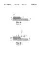
- FIGS. 1a-1dare an illustrational flow chart of the steps of forming an SNS Josephson junction according to a known process.
- FIGS. 2a-2dare an illustrational flow chart of the steps of forming an improved SSNS Josephson junction according to the present invention.
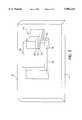
- FIG. 3is a perspective view of the SSNS junction of FIG. 2d.
- FIG. 4illustrates an improved SNS Josephson junction according to another embodiment of the present invention.
- the present inventionis directed to a high-temperature superconducting junction having improved quality and performance characteristics and a method of forming the junction.
- the superconducting junctioncan be a superconductive--superconductive-normal-superconductive (SSNS) junction 40 as shown in FIGS. 2d and 3, or a superconductive-normal-superconductive (SNS) junction 70 as shown in FIG. 4.
- SSNSsuperconductive--superconductive-normal-superconductive
- SNSsuperconductive-normal-superconductive
- FIGS. 1a-1dillustrate sequential steps of a known process for forming a known SNS junction structure 10.
- the processcomprises depositing a first high-T c superconductive (HTS) layer (base electrode layer) 12 and a dielectric layer 14 on a substrate 16.
- T cis the critical temperature below which superconductive materials exhibit zero electrical resistivity
- high-T c , superconductive materialsare materials that are superconductive above about 25 K.
- a photoresist layer 18is formed on the dielectric layer 14 and the photoresist layer 18 is then patterned to form an inclined surface 20. As depicted in FIG. 1b by arrows I, ion mill etching is then performed to remove a portion of the dielectric layer 14 and the first HTS layer 12 to define an inclined ramp edge 22 as shown in FIG. 1c.
- the photoresist layer 18is then stripped from the dielectric layer 14, typically using a wet chemical stripping process.
- the ex-situ wet stripping processcan contaminate and deoxygenate the ramp edge 22.
- Superconductive materialssuch as yttrium-barium-copper oxide (YBCO) are very reactive and exposed surfaces of thin films of these materials are easily contaminated by contact with air during photolithographic processing and, as a result, not able to support the growth of overlying deposited layers with the preferred crystal structure. In addition, the superconducting properties of the contaminated films can be degraded.
- YBCOyttrium-barium-copper oxide
- the ramp edge 22can be cleaned using a low-energy ion cleaning process to form the first HTS layer 12 and the dielectric layer 14.
- a barrier layer 24comprised of a normal material and a second high-T c , superconductive (HTS) layer 26 (counterelectrode layer) are sequentially deposited on the ramp edge 22.
- HTSsuperconductive
- normally materialsare materials that are non-superconductive at the temperature of operation of the Josephson junction.
- the SNS structureis patterned and defined using a conventional photoresist masking technique followed by ion-mill etching to form the SNS junction 10 shown in FIG. 1d.
- the c-axis directionis indicated by the arrow c.
- the current flow pathis to/from the first HTS layer 12 laterally in the direction of the a-axis (represented by arrow a in FIG. 1d) across the first HTS layer 12, and the barrier layer 24 to/from the second HTS layer 26.
- the low-energy ion cleaning of the ramp edge 22removes the top few contaminated monolayers of the first HTS layer 12, but also produces undesirable lattice damage in the ramp edge 22. Consequently, the structure and quality of the interface 28 between the first HTS layer 12 and the barrier layer 24 are degraded.
- the interface 28is resistive and/or non-uniform, which adversly impacted the uniformity of the characteristic voltage V c of the junction 10.
- V cI c R n , where I c is the critical Josephson junction current, the maximum supercurrent that the junction can sustain, and R n , is the electrical resistivity of the Josephson junction.
- the present inventionovercomes the problem of interfacial resistance associated with the known SNS Josephson junction 10 and provides a superconducting junction having improved operational performance.
- FIGS. 2d and 3illustrate a superconductive--superconductive-normal-superconductive (SSNS) Josephson junction 40 according to the present invention.
- the junction 40is formed on a substrate 42 having a planar upper surface 44.
- the junction 40comprises a first high-T c superconductive (HTS) layer 46 (first base electrode layer) comprised of a high-T c superconductive material provided on the upper surface 44 of the substrate 42, and a dielectric layer 48 disposed on the first HTS layer 46.
- the dielectric layer 48is comprised of a suitable dielectric material to provide electric insulation between the first HTS layer 46 and overlying layers as described below.
- the first HTS layer 46 and the dielectric layer 48define an inclined face referred to herein as the ramp edge 50.
- a trilayer SNS structure 52is disposed on the ramp edge 50.
- the trilayer SNS structure 52comprises a second high-T c , superconductive (HTS) layer 54 (second base electrode layer) of a high-T c superconductive material directly on the ramp edge 50, a barrier layer 56 of a normal material on the second HTS layer 54, and a third high-T c superconductive (HTS) layer 58 (counterelectrode layer) comprised of a high-T c superconductive material on the barrier layer 56.
- HTSsuperconductive
- the first HTS layer 46, second HTS layer 54 and third HTS layer 58are preferably epitaxial with a c-axis substantially normal to the upper surface 44 of the substrate 42 as represented by arrow c in FIG. 2d.
- the dielectric layer 48 and the barrier layer 56are typically also epitaxial with a c-axis in substantially the same direction as the superconductive layers.
- the ramp edge 50does not directly contact the barrier layer 56. Rather, the ramp edge 50 advantageously directly contacts the second HTS layer 54. As a result, the junction 40 eliminates the problem of electric resistance and non-uniformity at the interface 28 between the first HTS layer 12 and the barrier layer 24 in the known SNS junction 10.
- the present inventionovercomes the problems associated with known directional dependent processes.
- the high-T c SSNS Josephson junction 40provides strong phase coupling of the superconductive Cooper electron pairs between the first HTS layer 46 and the second HTS layer 54, and significantly reduces any detrimental effects caused by the presence of contamination at the interface 60 at the ramp edge 50.
- the trilayer SNS structure 52preserves the quality of the interface between the second HTS layer 54 and the barrier layer 56 and the interface between the barrier layer 56 and the third HTS layer 58.
- the resulting SSNS Josephson junction 40provides low interfacial electric resistance between the first HTS layer 46 and the second HTS layer 54, and enhanced I c R n , uniformity.
- FIGS. 2a-2dA method of forming the high-T c SSNS Josephson junction 40 according to the present invention is depicted in FIGS. 2a-2d.
- the SSNS Josephson junction 40is formed on the upper surface 44 of the substrate 42.
- the substrate 42is typically comprised of a dielectric material that, has lattice parameters closely matching that of the crystallographic face of the first HTS layer 46 perpendicular to the c-axis; i.e., the face in the a-axis direction.
- the substrate 42is typically a single crystal material.
- An excellent material for the substrate 42is lanthanum aluminate (LaAlO 3 ) which promotes c-axis epitaxial growth of YBa 2 Cu 3 O 7-X (YBCO).
- substrate 42 materials that promote c-axis epitaxial growth of YBCOcan also be used, including SrTiO 3 (strontium titanate), neodymium gallate, strontium aluminum tantalate and the like.
- SrTiO 3selectiveium titanate
- neodymium gallateneodymium gallate
- strontium aluminum tantalateneodymium aluminum tantalate
- the substrate 42can be comprised of LaAlO 3 and other suitable materials that promote c-axis epitaxial growth of the first HTS layer 46.
- the first HTS layer 46(first base electrode layer) is comprised of a high-T c superconductive material deposited as a thin film on the upper surface 44 of the substrate 42.
- the first HTS layer 46is typically comprised of a high-T c superconductive material selected from the YBCO system (YBa 2 Cu 3 O 7-x , where x is typically a low value of about 0.1). These materials have a critical temperature, T c , of about 85 K to about 92 K when deposited as a thin film. Other suitable high- c superconductive materials can be used to form the first HTS layer 46.
- the first HTS layer 46is epitaxially grown on the substrate 42 in the c-axis direction represented by arrow c, using a conventional thin film deposition process.
- a physical vapor deposition (PVD) processis used to restrict contamination levels.
- PVD processesinclude, for example, laser ablation, sputtering and the like.
- the first HTS layer 46typically has a thickness of from about 1000 ⁇ to about 4000 ⁇ .
- the dielectric layer 48is deposited on the first HTS layer 46 in-situ in the same deposition system.
- the dielectric layer 48is typically epitaxially grown in the c-axis direction using a suitable thin film deposition process such as, laser ablation, sputtering and the like.
- the dielectric layer 48is comprised of a suitable dielectric material such as SrTiO 3 , LaAlO 3 , neodymium gallate, strontium aluminum tantalate and the like.
- the dielectric layer 48typically has a thickness of from about 500 ⁇ to about 3000 ⁇ .
- a photoresist layer 62is deposited on the dielectric layer 48.
- the photoresist layer 62is comprised of a conventional material and is patterned using a conventional photoresist masking technique to enable the subsequent formation of the ramp edge 50 shown in FIGS. 2c and 2d.
- the ramp edge 50is typically formed by a conventional ion mill etching process. As shown in FIG. 2d, the ramp edge 50 is inclined upwardly at an angle ⁇ relative to the planar upper surface 44 of the substrate 42. This angle is typically from about 5° to about 90°, and preferably from about 5° to about 30°.
- the photoresist layer 62can be removed using a conventional wet stripping process performed at ambient conditions. This step can, however, contaminate the ramp edge 50 surface.
- the photoresist layer 62is preferably stripped in the same vacuum system and not exposed to room ambient conditions and wet etching chemicals. Particularly, instead of breaking vacuum and removing the as formed structure for wet etching, the structure is maintained within the vacuum system and the photoresist layer 62 is stripped in-situ by contact with a plasma generated from an oxygen containing gas such as O 2 Consequently, potential contamination of the ramp edge 50 surface is minimized.
- the plasma dry etch processcan reoxidize oxygen-depleted regions of the high-T c superconductive material forming the first HTS layer 46 to ensure a high-T c value is maintained.
- the plasma etch stepis preferably performed in the system used to subsequently form the trilayer SSNS structure 52.
- the plasma etch of the photoresist layer 62can be performed in a common vacuum chamber, or preferably in a dedicated vacuum chamber used for photoresist stripping, located within a multi-chamber, multi-function cluster tool system.
- a suitable cluster tool system for performing these stepsis the cluster tool system manufactured by DCA Inc.
- Other companies that manufacture cluster tool systemsincluded Applied Material, LAM Research, Leskers and the like.
- the plasma etch removal of the photoresist layer 62produces minimal chemical damage to the ramp edge 50.
- low-energy ion cleaningcan be used to clean the ramp edge 50 to remove any such minimal contamination before forming the trilayer SNS structure 52.
- the barrier layer 56 and the third HTS layer 58can be sequentially deposited on the ramp edge 50 to produce an SNS junction 70 shown in FIG. 4.
- the SNS junction 70has reduced interfacial resistance and increased uniformity between the first HTS layer 46 and the overlying barrier layer 56 as compared to the known SNS junction 10 shown in FIG. 1d.
- the trilayer SNS structure 52is formed on the ramp edge 50 to produce the SSNS junction 40.
- the trilayer SNS structure 52comprises the second HTS layer 54 (second base electrode layer) disposed directly on the ramp edge 50, the barrier layer 56 on the second HTS layer 54, and the third HTS layer 58 (counterelectrode layer) on the barrier layer 56.
- the trilayer SNS structure 52is preferably formed in-situ in the same system used to form the structure illustrated in FIG. 2c without breaking the vacuum; i.e., the same vacuum system, or alternately, a dedicated vacuum chamber for SNS film deposition within the same multi-chamber cluster tool system.
- the second HTS layer 54is deposited so that it overlies the ramp edge 50, the upper surface 44 of the substrate 42, and a portion of the upper surface 66 of the dielectric layer 48.
- the second HTS layer 54is preferably comprised of the same high-T c superconducting material as the first HTS layer 46 to provide matched lattice parameters, coefficients of thermal expansion and electrical properties, as well as chemical compatibility.
- the second HTS layer 54typically has a thickness of from about 100 ⁇ to about 1000 ⁇ , and preferably has a thickness of less than about 500 ⁇ . It is advantageous to maintain the second HTS layer 54 at a thickness of less than about 500 ⁇ so that the cross-sectional area of the second HTS layer 54 is maintained small also. If this cross-sectional area is too large, the portions of the second HTS layer 54, the barrier layer 56 and the third HTS layer 58 overlying the upper surface 66 of the dielectric layer 48 can function as part of the junction and effectively increase the junction geometry.
- the second HTS layer 54is preferably epitaxially grown in the c-axis direction using a suitable thin film deposition technique such as used to form the first HTS layer 46.
- the barrier layer 56is deposited on the second HTS layer 54.
- the barrier layer 56is comprised of a normal material that is non-superconductive at the temperature of operation of the SSNS junction 40. Suitable materials include cobalt-doped YBCO, cobalt-doped praseodymium barium copper oxide (cobalt-doped PBCO), gallium-doped PBCO and the like.
- the barrier layer 56typically has a thickness of from about 50 ⁇ to about 1000 ⁇ .
- the barrier layer 56is typically also epitaxially grown in the c-axis direction on the second HTS layer 54 using a suitable thin film deposition technique.
- the third HTS layer 58is deposited on the barrier layer 56.
- the third HTS layer 58is typically formed of the same high-T c superconductive material used to form the second HTS layer 54 and the first HTS layer 46.
- the third HTS layer 58typically has a thickness of from about 500 ⁇ to about 5000 ⁇ and is typically also epitaxially grown in the c-axis direction using a suitable thin film deposition technique.
- the third HTS layer 58can be deposited using the same thin film deposition technique used to form the first HTS layer 46 and the second HTS layer 54.
- the trilayer SNS structure 52is typically patterned and defined using a conventional photoresist masking technique followed by ion-mill etching, to produce the SSNS Josephson junction 40 as shown in FIG. 2d.
- an optional implant maskstepcan be performed after the trilayer SNS structure 52 is formed as depicted at 68 in FIG. 2d.
- the implant stepdelineates the junction region by implanting a suitable species such as silicon ions effective to destroy the superconductive characteristics of the second HTS layer 54 away from the trilayer SNS structure 52.
- a conventional ion implantation techniquecan be used to implant the species.
- the current flow pathis from/to the first HTS layer 46 laterally (in the a-axis direction) across the second HTS layer 54, and the barrier layer 56 laterally to/from the third HTS layer 58, as depicted by the arrow a in FIG. 2d.
- the thinness of the second HTS layer 54minimizes parasitic junction leakage current. Reduced phase coupling of superconducting current Cooper pairs in the c-axis direction significantly reduces the parasitic junction leakage current.
- the present SSNS Josephson junction 40has reduced base electrode layer (second HTS layer 54) to barrier layer 56 interface electrical resistance, enhanced I c , and enhanced V c uniformity.
- an SSNS junction 40including a first HTS layer 46, a second HTS layer 54 and a third HTS layer 58 comprised of YBCO, an upper layer comprised of strontium titanate, a normal barrier layer 56 comprised of cobalt-doped YBCO, and having a width of about 4 microns typically has a I c value of from about 100 microamps to about 500 microamps, and a V c value of from about 100 microvolts to about 400 microvolts.
- the present inventioncan be used in HTS integrated circuits having enhanced gate complexity.
- the high V c of the present inventionenables larger signal values for improved output driving capability and improved immunity against background noise, and also high speed of operation.
- the base electrode formed of the first HTS layer 46 and the second HTS layer 54, and the counterelectrode (third HTS) layer 58can be used as separate interconnect layers, allowing one layer to cross over the other layer.
Landscapes
- Engineering & Computer Science (AREA)
- Chemical & Material Sciences (AREA)
- Ceramic Engineering (AREA)
- Manufacturing & Machinery (AREA)
- Superconductor Devices And Manufacturing Methods Thereof (AREA)
Abstract
Description
Claims (9)
Priority Applications (3)
| Application Number | Priority Date | Filing Date | Title |
|---|---|---|---|
| US08/761,412US5892243A (en) | 1996-12-06 | 1996-12-06 | High-temperature SSNS and SNS Josephson junction and method of making junction |
| JP9333051AJP3031884B2 (en) | 1996-12-06 | 1997-12-03 | High temperature SSNS and SNS Josephson junction and manufacturing method thereof |
| US09/012,090US6066600A (en) | 1996-12-06 | 1998-01-22 | Method of making high-Tc SSNS and SNS Josephson junction |
Applications Claiming Priority (1)
| Application Number | Priority Date | Filing Date | Title |
|---|---|---|---|
| US08/761,412US5892243A (en) | 1996-12-06 | 1996-12-06 | High-temperature SSNS and SNS Josephson junction and method of making junction |
Related Child Applications (1)
| Application Number | Title | Priority Date | Filing Date |
|---|---|---|---|
| US09/012,090DivisionUS6066600A (en) | 1996-12-06 | 1998-01-22 | Method of making high-Tc SSNS and SNS Josephson junction |
Publications (1)
| Publication Number | Publication Date |
|---|---|
| US5892243Atrue US5892243A (en) | 1999-04-06 |
Family
ID=25062099
Family Applications (2)
| Application Number | Title | Priority Date | Filing Date |
|---|---|---|---|
| US08/761,412Expired - Fee RelatedUS5892243A (en) | 1996-12-06 | 1996-12-06 | High-temperature SSNS and SNS Josephson junction and method of making junction |
| US09/012,090Expired - Fee RelatedUS6066600A (en) | 1996-12-06 | 1998-01-22 | Method of making high-Tc SSNS and SNS Josephson junction |
Family Applications After (1)
| Application Number | Title | Priority Date | Filing Date |
|---|---|---|---|
| US09/012,090Expired - Fee RelatedUS6066600A (en) | 1996-12-06 | 1998-01-22 | Method of making high-Tc SSNS and SNS Josephson junction |
Country Status (2)
| Country | Link |
|---|---|
| US (2) | US5892243A (en) |
| JP (1) | JP3031884B2 (en) |
Cited By (23)
| Publication number | Priority date | Publication date | Assignee | Title |
|---|---|---|---|---|
| US6004907A (en)* | 1997-11-20 | 1999-12-21 | Electronics And Telecommunications Research Institute | Method of fabricating a superconducting junction using cubic YBa2 Cu3 O x thin film as a barrier layer |
| US6188919B1 (en)* | 1999-05-19 | 2001-02-13 | Trw Inc. | Using ion implantation to create normal layers in superconducting-normal-superconducting Josephson junctions |
| US6541789B1 (en)* | 1998-09-01 | 2003-04-01 | Nec Corporation | High temperature superconductor Josephson junction element and manufacturing method for the same |
| US20040077504A1 (en)* | 2001-08-22 | 2004-04-22 | Seiji Adachi | High temperature superconducting josephson junctin, superconducting electronic device provided with the former and method of manufacturing high temperature superconducting josephson junction |
| US6734699B1 (en) | 1999-07-14 | 2004-05-11 | Northrop Grumman Corporation | Self-clocked complementary logic |
| US6753546B2 (en) | 2001-08-29 | 2004-06-22 | D-Wave Systems, Inc. | Trilayer heterostructure Josephson junctions |
| US20040134967A1 (en)* | 1997-05-22 | 2004-07-15 | Conductis, Inc. | Interface engineered high-Tc Josephson junctions |
| US20040266627A1 (en)* | 1997-05-22 | 2004-12-30 | Moeckly Brian H. | High-temperature superconductor devices and methods of forming the same |
| US20050040843A1 (en)* | 2003-08-20 | 2005-02-24 | Eaton Larry Rodney | Superconducting constant current source |
| US20050062131A1 (en)* | 2003-09-24 | 2005-03-24 | Murduck James Matthew | A1/A1Ox/A1 resistor process for integrated circuits |
| US20060247131A1 (en)* | 2003-03-28 | 2006-11-02 | Fujitsu Limited | High-temperature superconducting device and manufacturing method thereof |
| WO2009101257A1 (en)* | 2008-02-15 | 2009-08-20 | Teknillinen Korkeakoulu | Proximity josephson sensor |
| US9648749B1 (en) | 2015-11-17 | 2017-05-09 | Northrop Grumman Systems Corporation | Circuit card assembly and method of providing same |
| US10367134B2 (en)* | 2017-06-07 | 2019-07-30 | International Business Machines Corporation | Shadow mask sidewall tunnel junction for quantum computing |
| CN111613661A (en)* | 2019-02-22 | 2020-09-01 | 中国科学院物理研究所 | Tunnel junction, its preparation method and application |
| CN111933788A (en)* | 2020-08-11 | 2020-11-13 | 中国科学院紫金山天文台 | Method for preparing high-quality superconducting tunnel junction circuit |
| US11856871B2 (en) | 2018-11-13 | 2023-12-26 | D-Wave Systems Inc. | Quantum processors |
| US11930721B2 (en) | 2012-03-08 | 2024-03-12 | 1372934 B.C. Ltd. | Systems and methods for fabrication of superconducting integrated circuits |
| US11957065B2 (en) | 2017-02-01 | 2024-04-09 | 1372934 B.C. Ltd. | Systems and methods for fabrication of superconducting integrated circuits |
| US12102017B2 (en) | 2019-02-15 | 2024-09-24 | D-Wave Systems Inc. | Kinetic inductance for couplers and compact qubits |
| US12367412B2 (en) | 2019-12-05 | 2025-07-22 | 1372934 B.C. Ltd. | Systems and methods for fabricating flux trap mitigating superconducting integrated circuits |
| US12376501B2 (en) | 2020-05-11 | 2025-07-29 | 1372934 B.C. Ltd. | Kinetic inductance devices, methods for fabricating kinetic inductance devices, and articles employing the same |
| US12392823B2 (en) | 2021-11-05 | 2025-08-19 | D-Wave Systems Inc. | Systems and methods for on-chip noise measurements |
Families Citing this family (9)
| Publication number | Priority date | Publication date | Assignee | Title |
|---|---|---|---|---|
| US5892243A (en)* | 1996-12-06 | 1999-04-06 | Trw Inc. | High-temperature SSNS and SNS Josephson junction and method of making junction |
| US5889289A (en)* | 1997-08-28 | 1999-03-30 | The United States Of America As Represented By The Secretary Of The Navy | High temperature superconductor/insulator composite thin films with Josephson coupled grains |
| KR100386454B1 (en)* | 2001-06-29 | 2003-06-02 | 주식회사 하이닉스반도체 | Method for forming the semiconductor device |
| US6734454B2 (en) | 2001-08-27 | 2004-05-11 | The Regents Of The University Of California | Internally shunted Josephson junction device |
| KR100459125B1 (en)* | 2002-02-28 | 2004-12-03 | 엘지전자 주식회사 | Manufacturing method for divice junction Josephson superconductor |
| KR20030071300A (en)* | 2002-02-28 | 2003-09-03 | 엘지전자 주식회사 | Manufacturing method for divice junction Josephson superconductor |
| JP2003282981A (en)* | 2002-03-26 | 2003-10-03 | Fujitsu Ltd | Josephson junction device and method of manufacturing the same |
| US8055318B1 (en)* | 2008-04-23 | 2011-11-08 | Hypres, Inc. | Superconducting integrated circuit technology using iron-arsenic compounds |
| US9355362B2 (en)* | 2011-11-11 | 2016-05-31 | Northrop Grumman Systems Corporation | Quantum bits and method of forming the same |
Citations (22)
| Publication number | Priority date | Publication date | Assignee | Title |
|---|---|---|---|---|
| US4414738A (en)* | 1981-02-02 | 1983-11-15 | The United States Of America As Represented By The Secretary Of The Navy | Optical lithographic technique for fabricating submicron-sized Josephson microbridges |
| US4432134A (en)* | 1982-05-10 | 1984-02-21 | Rockwell International Corporation | Process for in-situ formation of niobium-insulator-niobium Josephson tunnel junction devices |
| US4454522A (en)* | 1981-11-05 | 1984-06-12 | The Board Of Trustees Of The Leland Stanford Junior University | Microbridge superconducting device having support with stepped parallel surfaces |
| US5134117A (en)* | 1991-01-22 | 1992-07-28 | Biomagnetic Technologies, Inc. | High tc microbridge superconductor device utilizing stepped edge-to-edge sns junction |
| US5256636A (en)* | 1990-09-21 | 1993-10-26 | The Regents Of The University Of Calif. | Microelectronic superconducting device with multi-layer contact |
| US5266558A (en)* | 1991-05-01 | 1993-11-30 | International Business Machines Corporation | Superconducting circuit elements with metallic substrate and method for manufacturing the same |
| US5280013A (en)* | 1991-07-05 | 1994-01-18 | Conductus, Inc. | Method of preparing high temperature superconductor films on opposite sides of a substrate |
| US5291035A (en)* | 1990-03-09 | 1994-03-01 | The Regents Of The University Of California | Microelectronic superconducting crossover and coil |
| US5322817A (en)* | 1990-10-16 | 1994-06-21 | Superconductor Technologies, Inc. | In situ growth of TL-containing oxide superconducting films |
| US5378683A (en)* | 1991-04-23 | 1995-01-03 | Thomson-Csf | Josephson junction structure |
| US5389606A (en)* | 1992-03-13 | 1995-02-14 | E. I. Du Pont De Nemours And Company | Process for producing thin films of inorganic oxides of controlled stoichiometry |
| US5399881A (en)* | 1993-04-30 | 1995-03-21 | Varian Associates, Inc. | High-temperature Josephson junction and method |
| US5430014A (en)* | 1991-11-02 | 1995-07-04 | Forschungszentrum Julich Gmbh | Method of producing an SrTiO3 /YBa2 Cu3 O7 layer system and a layer system as thus produced as a high-temperature superconductor |
| US5432149A (en)* | 1992-06-22 | 1995-07-11 | Regents Of The University Of California | In-situ tunable Josephson weak links |
| US5439877A (en)* | 1990-12-07 | 1995-08-08 | E. I. Du Pont De Nemours And Company | Process for depositing high temperature superconducting oxide thin films |
| US5472934A (en)* | 1993-07-30 | 1995-12-05 | Agency Of Industrial Science & Technology | Anisotropic superconducting device and fluxon device |
| US5488030A (en)* | 1990-09-20 | 1996-01-30 | Sumitomo Electric Industries, Inc. | Superconductor junction structure including two oxide superconductor layers separated by a non-superconducting layer |
| US5508255A (en)* | 1994-07-05 | 1996-04-16 | Superconductor Technologies, Inc. | Epitaxial thallium high temperature superconducting films formed via a nucleation layer |
| US5523283A (en)* | 1988-08-18 | 1996-06-04 | Trw Inc. | La AlO3 Substrate for copper oxide superconductors |
| US5534491A (en)* | 1991-03-28 | 1996-07-09 | Sumitomo Electric Industries, Ltd. | Process for preparing a layered structure containing at least one thin film of oxide superconductor |
| US5627139A (en)* | 1990-09-24 | 1997-05-06 | The Regents Of The University Of California | High-temperature superconducting josephson devices having a barrier layer of a doped, cubic crystalline, conductive oxide material |
| US5696392A (en)* | 1992-09-14 | 1997-12-09 | Conductus, Inc. | Barrier layers for oxide superconductor devices and circuits |
Family Cites Families (3)
| Publication number | Priority date | Publication date | Assignee | Title |
|---|---|---|---|---|
| GB2288094A (en)* | 1994-03-25 | 1995-10-04 | Secr Defence | Superconductive junction |
| KR0175359B1 (en)* | 1995-12-15 | 1999-02-01 | 양승택 | Method for fabricating superconductor-insulator-superconductor josephson tunnel junction structure |
| US5892243A (en)* | 1996-12-06 | 1999-04-06 | Trw Inc. | High-temperature SSNS and SNS Josephson junction and method of making junction |
- 1996
- 1996-12-06USUS08/761,412patent/US5892243A/ennot_activeExpired - Fee Related
- 1997
- 1997-12-03JPJP9333051Apatent/JP3031884B2/ennot_activeExpired - Fee Related
- 1998
- 1998-01-22USUS09/012,090patent/US6066600A/ennot_activeExpired - Fee Related
Patent Citations (23)
| Publication number | Priority date | Publication date | Assignee | Title |
|---|---|---|---|---|
| US4414738A (en)* | 1981-02-02 | 1983-11-15 | The United States Of America As Represented By The Secretary Of The Navy | Optical lithographic technique for fabricating submicron-sized Josephson microbridges |
| US4454522A (en)* | 1981-11-05 | 1984-06-12 | The Board Of Trustees Of The Leland Stanford Junior University | Microbridge superconducting device having support with stepped parallel surfaces |
| US4432134A (en)* | 1982-05-10 | 1984-02-21 | Rockwell International Corporation | Process for in-situ formation of niobium-insulator-niobium Josephson tunnel junction devices |
| US5523283A (en)* | 1988-08-18 | 1996-06-04 | Trw Inc. | La AlO3 Substrate for copper oxide superconductors |
| US5291035A (en)* | 1990-03-09 | 1994-03-01 | The Regents Of The University Of California | Microelectronic superconducting crossover and coil |
| US5488030A (en)* | 1990-09-20 | 1996-01-30 | Sumitomo Electric Industries, Inc. | Superconductor junction structure including two oxide superconductor layers separated by a non-superconducting layer |
| US5256636A (en)* | 1990-09-21 | 1993-10-26 | The Regents Of The University Of Calif. | Microelectronic superconducting device with multi-layer contact |
| US5627139A (en)* | 1990-09-24 | 1997-05-06 | The Regents Of The University Of California | High-temperature superconducting josephson devices having a barrier layer of a doped, cubic crystalline, conductive oxide material |
| US5322817A (en)* | 1990-10-16 | 1994-06-21 | Superconductor Technologies, Inc. | In situ growth of TL-containing oxide superconducting films |
| US5439877A (en)* | 1990-12-07 | 1995-08-08 | E. I. Du Pont De Nemours And Company | Process for depositing high temperature superconducting oxide thin films |
| US5367178A (en)* | 1991-01-22 | 1994-11-22 | Biomagnetic Technologies, Inc. | High-TC microbridge superconductor device utilizing stepped edge-to-edge SNS junction |
| US5134117A (en)* | 1991-01-22 | 1992-07-28 | Biomagnetic Technologies, Inc. | High tc microbridge superconductor device utilizing stepped edge-to-edge sns junction |
| US5534491A (en)* | 1991-03-28 | 1996-07-09 | Sumitomo Electric Industries, Ltd. | Process for preparing a layered structure containing at least one thin film of oxide superconductor |
| US5378683A (en)* | 1991-04-23 | 1995-01-03 | Thomson-Csf | Josephson junction structure |
| US5266558A (en)* | 1991-05-01 | 1993-11-30 | International Business Machines Corporation | Superconducting circuit elements with metallic substrate and method for manufacturing the same |
| US5280013A (en)* | 1991-07-05 | 1994-01-18 | Conductus, Inc. | Method of preparing high temperature superconductor films on opposite sides of a substrate |
| US5430014A (en)* | 1991-11-02 | 1995-07-04 | Forschungszentrum Julich Gmbh | Method of producing an SrTiO3 /YBa2 Cu3 O7 layer system and a layer system as thus produced as a high-temperature superconductor |
| US5389606A (en)* | 1992-03-13 | 1995-02-14 | E. I. Du Pont De Nemours And Company | Process for producing thin films of inorganic oxides of controlled stoichiometry |
| US5432149A (en)* | 1992-06-22 | 1995-07-11 | Regents Of The University Of California | In-situ tunable Josephson weak links |
| US5696392A (en)* | 1992-09-14 | 1997-12-09 | Conductus, Inc. | Barrier layers for oxide superconductor devices and circuits |
| US5399881A (en)* | 1993-04-30 | 1995-03-21 | Varian Associates, Inc. | High-temperature Josephson junction and method |
| US5472934A (en)* | 1993-07-30 | 1995-12-05 | Agency Of Industrial Science & Technology | Anisotropic superconducting device and fluxon device |
| US5508255A (en)* | 1994-07-05 | 1996-04-16 | Superconductor Technologies, Inc. | Epitaxial thallium high temperature superconducting films formed via a nucleation layer |
Non-Patent Citations (2)
| Title |
|---|
| Strikovskiy, M.D. et al., "Ramp-type YBa2 Cu3 O7-δ Josephson junctions with high characteristic voltage, fabricated by a new, completely in situ, growth technique," Appl. Phys. Lett. 69(19):2918-2920 (1996). |
| Strikovskiy, M.D. et al., Ramp type YBa 2 Cu 3 O 7 Josephson junctions with high characteristic voltage, fabricated by a new, completely in situ, growth technique, Appl. Phys. Lett. 69(19):2918 2920 (1996).* |
Cited By (31)
| Publication number | Priority date | Publication date | Assignee | Title |
|---|---|---|---|---|
| US20040134967A1 (en)* | 1997-05-22 | 2004-07-15 | Conductis, Inc. | Interface engineered high-Tc Josephson junctions |
| US20040266627A1 (en)* | 1997-05-22 | 2004-12-30 | Moeckly Brian H. | High-temperature superconductor devices and methods of forming the same |
| US6004907A (en)* | 1997-11-20 | 1999-12-21 | Electronics And Telecommunications Research Institute | Method of fabricating a superconducting junction using cubic YBa2 Cu3 O x thin film as a barrier layer |
| US6541789B1 (en)* | 1998-09-01 | 2003-04-01 | Nec Corporation | High temperature superconductor Josephson junction element and manufacturing method for the same |
| US6188919B1 (en)* | 1999-05-19 | 2001-02-13 | Trw Inc. | Using ion implantation to create normal layers in superconducting-normal-superconducting Josephson junctions |
| US6734699B1 (en) | 1999-07-14 | 2004-05-11 | Northrop Grumman Corporation | Self-clocked complementary logic |
| US20040077504A1 (en)* | 2001-08-22 | 2004-04-22 | Seiji Adachi | High temperature superconducting josephson junctin, superconducting electronic device provided with the former and method of manufacturing high temperature superconducting josephson junction |
| US6999806B2 (en)* | 2001-08-22 | 2006-02-14 | International Superconductivity Technology Center, The Juridical Foundation | High temperature superconducting josephson junctin, superconducting electronic device provided with the former and method of manufacturing high temperature superconducting josephson junction |
| US6753546B2 (en) | 2001-08-29 | 2004-06-22 | D-Wave Systems, Inc. | Trilayer heterostructure Josephson junctions |
| US20060247131A1 (en)* | 2003-03-28 | 2006-11-02 | Fujitsu Limited | High-temperature superconducting device and manufacturing method thereof |
| US20050040843A1 (en)* | 2003-08-20 | 2005-02-24 | Eaton Larry Rodney | Superconducting constant current source |
| US7002366B2 (en) | 2003-08-20 | 2006-02-21 | Northrop Grumman Corporation | Superconducting constant current source |
| US20050062131A1 (en)* | 2003-09-24 | 2005-03-24 | Murduck James Matthew | A1/A1Ox/A1 resistor process for integrated circuits |
| WO2009101257A1 (en)* | 2008-02-15 | 2009-08-20 | Teknillinen Korkeakoulu | Proximity josephson sensor |
| US11930721B2 (en) | 2012-03-08 | 2024-03-12 | 1372934 B.C. Ltd. | Systems and methods for fabrication of superconducting integrated circuits |
| US9648749B1 (en) | 2015-11-17 | 2017-05-09 | Northrop Grumman Systems Corporation | Circuit card assembly and method of providing same |
| WO2017087093A1 (en)* | 2015-11-17 | 2017-05-26 | Northrop Grumman Systems Corporation | Circuit card assembly and method of providing same |
| US11957065B2 (en) | 2017-02-01 | 2024-04-09 | 1372934 B.C. Ltd. | Systems and methods for fabrication of superconducting integrated circuits |
| US10790433B2 (en) | 2017-06-07 | 2020-09-29 | International Business Machines Corporation | Shadow mask sidewall tunnel junction for quantum computing |
| US10367134B2 (en)* | 2017-06-07 | 2019-07-30 | International Business Machines Corporation | Shadow mask sidewall tunnel junction for quantum computing |
| US11069849B2 (en) | 2017-06-07 | 2021-07-20 | International Business Machines Corporation | Shadow mask sidewall tunnel junction for quantum computing |
| US10707401B2 (en) | 2017-06-07 | 2020-07-07 | International Business Machines Corporation | Shadow mask sidewall tunnel junction for quantum computing |
| US11856871B2 (en) | 2018-11-13 | 2023-12-26 | D-Wave Systems Inc. | Quantum processors |
| US12102017B2 (en) | 2019-02-15 | 2024-09-24 | D-Wave Systems Inc. | Kinetic inductance for couplers and compact qubits |
| CN111613661A (en)* | 2019-02-22 | 2020-09-01 | 中国科学院物理研究所 | Tunnel junction, its preparation method and application |
| CN111613661B (en)* | 2019-02-22 | 2024-03-26 | 中国科学院物理研究所 | Tunnel junction, preparation method and application thereof |
| US12367412B2 (en) | 2019-12-05 | 2025-07-22 | 1372934 B.C. Ltd. | Systems and methods for fabricating flux trap mitigating superconducting integrated circuits |
| US12376501B2 (en) | 2020-05-11 | 2025-07-29 | 1372934 B.C. Ltd. | Kinetic inductance devices, methods for fabricating kinetic inductance devices, and articles employing the same |
| CN111933788A (en)* | 2020-08-11 | 2020-11-13 | 中国科学院紫金山天文台 | Method for preparing high-quality superconducting tunnel junction circuit |
| CN111933788B (en)* | 2020-08-11 | 2024-05-31 | 中国科学院紫金山天文台 | Method for preparing high-quality superconducting tunnel junction circuit |
| US12392823B2 (en) | 2021-11-05 | 2025-08-19 | D-Wave Systems Inc. | Systems and methods for on-chip noise measurements |
Also Published As
| Publication number | Publication date |
|---|---|
| US6066600A (en) | 2000-05-23 |
| JP3031884B2 (en) | 2000-04-10 |
| JPH10173246A (en) | 1998-06-26 |
Similar Documents
| Publication | Publication Date | Title |
|---|---|---|
| US5892243A (en) | High-temperature SSNS and SNS Josephson junction and method of making junction | |
| US5236896A (en) | Superconducting device having an extremely thin superconducting channel formed of oxide superconductor material | |
| EP0673073B1 (en) | Method of manufacturing a superconducting device | |
| US5047390A (en) | Josephson devices and process for manufacturing the same | |
| JP3278638B2 (en) | High-temperature superconducting Josephson junction and method of manufacturing the same | |
| US5407903A (en) | Superconducting device having a reduced thickness of oxide superconducting layer | |
| US5250817A (en) | Alkali barrier superconductor Josephson junction and circuit | |
| EP0484253B1 (en) | Superconducting device having an extremely thin superconducting channel formed of oxide superconductor material and method for manufacturing the same | |
| EP0421889B1 (en) | Method for forming a continuous oxide superconductor layer having different thickness portions for superconductor device | |
| US5776863A (en) | In-situ fabrication of a superconductor hetero-epitaxial Josephson junction | |
| EP0506582B1 (en) | Process for preparing layered thin films | |
| CA2051048C (en) | Superconducting device having a reduced thickness of oxide superconducting layer and method for manufacturing the same | |
| EP0477103B1 (en) | Method for manufacturing superconducting device having a reduced thickness of oxide superconducting layer and superconducting device manufactured thereby | |
| EP0546904B1 (en) | Method for manufacturing an artificial grain boundary type Josephson junction device | |
| EP0484232B1 (en) | Superconducting device having an extremely short superconducting channel formed of oxide superconductor material and method for manufacturing the same | |
| EP0508844B1 (en) | Superconducting thin film having at least one isolated superconducting region formed of oxide superconductor material and method for manufacturing the same | |
| EP0506573B1 (en) | Process for cleaning a surface of thin film of oxide superconductor | |
| EP0422641B1 (en) | Superconductor device | |
| EP0534811A2 (en) | Method of manufacturing superconducting thin film formed of oxide superconductor having non superconducting region in it, and method of manufacturing superconducting device utilizing the superconducting thin film | |
| EP0509886B1 (en) | Process for patterning layered thin films including a superconductor layer | |
| JP2908346B2 (en) | Superconducting structure | |
| JP3186035B2 (en) | Laminated thin film for field effect element and field effect transistor using the laminated thin film | |
| JPH04284632A (en) | How to form superconductor lines | |
| EP0790655B1 (en) | Superconducting field effect device having a superconducting channel and method for manufacturing the same | |
| KR100233845B1 (en) | Twin-crystal-grain-boundary-junction superconducting field effect device and manufacturing method thereof |
Legal Events
| Date | Code | Title | Description |
|---|---|---|---|
| AS | Assignment | Owner name:TRW INC., CALIFORNIA Free format text:ASSIGNMENT OF ASSIGNORS INTEREST;ASSIGNOR:CHAN, HUGO WAI-KUNG;REEL/FRAME:008353/0744 Effective date:19961205 | |
| FPAY | Fee payment | Year of fee payment:4 | |
| AS | Assignment | Owner name:NORTHROP GRUMMAN CORPORATION, CALIFORNIA Free format text:ASSIGNMENT OF ASSIGNORS INTEREST;ASSIGNOR:TRW, INC. N/K/A NORTHROP GRUMMAN SPACE AND MISSION SYSTEMS CORPORATION, AN OHIO CORPORATION;REEL/FRAME:013751/0849 Effective date:20030122 Owner name:NORTHROP GRUMMAN CORPORATION,CALIFORNIA Free format text:ASSIGNMENT OF ASSIGNORS INTEREST;ASSIGNOR:TRW, INC. N/K/A NORTHROP GRUMMAN SPACE AND MISSION SYSTEMS CORPORATION, AN OHIO CORPORATION;REEL/FRAME:013751/0849 Effective date:20030122 | |
| FPAY | Fee payment | Year of fee payment:8 | |
| FEPP | Fee payment procedure | Free format text:PAYOR NUMBER ASSIGNED (ORIGINAL EVENT CODE: ASPN); ENTITY STATUS OF PATENT OWNER: LARGE ENTITY | |
| AS | Assignment | Owner name:NORTHROP GRUMMAN SPACE & MISSION SYSTEMS CORP.,CAL Free format text:ASSIGNMENT OF ASSIGNORS INTEREST;ASSIGNOR:NORTHROP GRUMMAN CORPORTION;REEL/FRAME:023699/0551 Effective date:20091125 Owner name:NORTHROP GRUMMAN SPACE & MISSION SYSTEMS CORP., CA Free format text:ASSIGNMENT OF ASSIGNORS INTEREST;ASSIGNOR:NORTHROP GRUMMAN CORPORTION;REEL/FRAME:023699/0551 Effective date:20091125 | |
| AS | Assignment | Owner name:NORTHROP GRUMMAN SYSTEMS CORPORATION,CALIFORNIA Free format text:ASSIGNMENT OF ASSIGNORS INTEREST;ASSIGNOR:NORTHROP GRUMMAN SPACE & MISSION SYSTEMS CORP.;REEL/FRAME:023915/0446 Effective date:20091210 Owner name:NORTHROP GRUMMAN SYSTEMS CORPORATION, CALIFORNIA Free format text:ASSIGNMENT OF ASSIGNORS INTEREST;ASSIGNOR:NORTHROP GRUMMAN SPACE & MISSION SYSTEMS CORP.;REEL/FRAME:023915/0446 Effective date:20091210 | |
| REMI | Maintenance fee reminder mailed | ||
| LAPS | Lapse for failure to pay maintenance fees | ||
| LAPS | Lapse for failure to pay maintenance fees | Free format text:PATENT EXPIRED FOR FAILURE TO PAY MAINTENANCE FEES (ORIGINAL EVENT CODE: EXP.); ENTITY STATUS OF PATENT OWNER: LARGE ENTITY | |
| STCH | Information on status: patent discontinuation | Free format text:PATENT EXPIRED DUE TO NONPAYMENT OF MAINTENANCE FEES UNDER 37 CFR 1.362 | |
| FP | Lapsed due to failure to pay maintenance fee | Effective date:20110406 |