US5889571A - Ultraviolet irradiating device for photo-alignment process and an irradiating method using the same - Google Patents
Ultraviolet irradiating device for photo-alignment process and an irradiating method using the sameDownload PDFInfo
- Publication number
- US5889571A US5889571AUS08/792,265US79226597AUS5889571AUS 5889571 AUS5889571 AUS 5889571AUS 79226597 AUS79226597 AUS 79226597AUS 5889571 AUS5889571 AUS 5889571A
- Authority
- US
- United States
- Prior art keywords
- photo
- light
- alignment layer
- irradiating
- alignment
- Prior art date
- Legal status (The legal status is an assumption and is not a legal conclusion. Google has not performed a legal analysis and makes no representation as to the accuracy of the status listed.)
- Expired - Lifetime
Links
Images

Classifications
- G—PHYSICS
- G02—OPTICS
- G02F—OPTICAL DEVICES OR ARRANGEMENTS FOR THE CONTROL OF LIGHT BY MODIFICATION OF THE OPTICAL PROPERTIES OF THE MEDIA OF THE ELEMENTS INVOLVED THEREIN; NON-LINEAR OPTICS; FREQUENCY-CHANGING OF LIGHT; OPTICAL LOGIC ELEMENTS; OPTICAL ANALOGUE/DIGITAL CONVERTERS
- G02F1/00—Devices or arrangements for the control of the intensity, colour, phase, polarisation or direction of light arriving from an independent light source, e.g. switching, gating or modulating; Non-linear optics
- G02F1/01—Devices or arrangements for the control of the intensity, colour, phase, polarisation or direction of light arriving from an independent light source, e.g. switching, gating or modulating; Non-linear optics for the control of the intensity, phase, polarisation or colour
- G02F1/13—Devices or arrangements for the control of the intensity, colour, phase, polarisation or direction of light arriving from an independent light source, e.g. switching, gating or modulating; Non-linear optics for the control of the intensity, phase, polarisation or colour based on liquid crystals, e.g. single liquid crystal display cells
- G02F1/133—Constructional arrangements; Operation of liquid crystal cells; Circuit arrangements
- G02F1/1333—Constructional arrangements; Manufacturing methods
- G02F1/1337—Surface-induced orientation of the liquid crystal molecules, e.g. by alignment layers
- G02F1/13378—Surface-induced orientation of the liquid crystal molecules, e.g. by alignment layers by treatment of the surface, e.g. embossing, rubbing or light irradiation
- G02F1/133788—Surface-induced orientation of the liquid crystal molecules, e.g. by alignment layers by treatment of the surface, e.g. embossing, rubbing or light irradiation by light irradiation, e.g. linearly polarised light photo-polymerisation
Definitions
- the present inventionrelates to an ultraviolet irradiating device and related method, and more particularly to an apparatus for a photo-alignment process in which the UV light is uniformly and widely irradiated into the alignment layer to obtain a large size liquid crystal display.
- a conventionally used liquid crystal displayis mainly a twisted nematic liquid crystal display (referred as TNLCD), which has a changeable transmittance at each gray level according to the viewing angle.
- TNLCDtwisted nematic liquid crystal display
- the transmittanceis symmetrical in the horizontal direction
- the transmittanceis asymmetrical in the vertical direction. Therefore, in the vertical direction, a range with an inverted image phenomenon occurs so that the vertical viewing angle becomes very limited.
- a multi-domain liquid crystal cellin which a pixel is divided into more than two pretilts where the pretilt defines pretilt angle and pretilt direction, is introduced.
- a reverse rubbing methodis too complicated because it comprises the following steps: rubbing the entire alignment layer in a first rubbing direction; applying a photoresist as a mask for blocking one domain; rubbing the other domain in a reverse direction to the first rubbing direction; and removing the photoresist.
- Using a reverse rubbing processgenerates dust and/or an electrostatic discharge, thus reducing productivity and/or damaging the thin film transistor which drives a pixel.
- each pixelis divided into more than 4 domains.
- a photo-alignment methodis used.
- the pretiltdefining a pretilt angle and a pretilt angle direction
- the fabricating processis simple and the damage to the substrate can be prevented.
- the photopolymeris photopolymerized by the cross linking generated between the polymers. Therefore, a pretilt on the alignment layer is determined according to the direction and the degree of cross linking of the photopolymers; the cross linking depending on the polarization direction, the incident direction of the light, and the amount of photo-energy of the light absorbed into the alignment layer.
- the direction and the magnitude of the pretiltare determined according to the polarization direction of the UV light and the photo-energy absorbed into the alignment layer.
- each domainis respectively exposed to UV light having a different polarization direction and a different photo-energy. Therefore, it is important to conform the uniformity of photo-energy absorbed into the alignment layer as well as the size of the spot of the light to make a large size liquid crystal display.
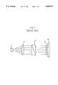
- FIG. 1is a view showing the conventional UV light irradiating apparatus.
- the UV light generated from a UV lamp 1is focused by a lens 2 and then linearly polarized by a polarizer 3. These elements are arranged in a line with a substrate 4.
- the substrate 4, coated with an alignment layer 5 that can be photo-reacted,is exposed by the circular spot of the UV light, so that a pretilt is given to the alignment layer 5 formed on the substrate 4.
- Irradiating UV light to the alignment layer 5 by the conventional UV irradiating apparatusis limited by the size of the UV lamp 1, so the exposed circular area 6 on the alignment layer 5 is also small as shown in FIG. 2a.
- the available alignment layer sizeis smaller than the area corresponding the plateau of the graph of FIG. 2b having a uniform photo-energy.
- the available alignment layer sizeis restricted by the size of the lamp.
- a UV irradiating apparatusincludes a UV lamp generating the UV light, a lens, a polarizer in which the UV light is linearly polarized, and a substrate coated with an alignment layer including a photo-reacting polymer such as polysiloxane based materials.
- the UV lamp, the lens, and the polarizerare arranged in a line, above the substrate.
- the UV lightis irradiated into the substrate at a certain angle with respect to the substrate. Accordingly, the alignment layer is exposed by an elliptical spot of UV light larger than the conventional exposed area.
- the UV lamp, the lens, and the polarizerare mounted into a casing and moved above the substrate by a scan motor to scan the whole area of the alignment layer uniformly.
- the irradiated spot of lightis moved out of the alignment layer to provide uniformity to the peripheral alignment layer.
- the spot of lightis moved to the next line, where the distance between adjacent lines is within 5 mm to guarantee beam uniformity.
- the photo-energy amount absorbed into the whole alignment layeris uniform.
- FIG. 1is a view showing the conventional UV light irradiating apparatus for a photo-alignment process.
- FIG. 2ais a plan view showing the spot of the UV light irradiated into the alignment layer when the conventional UV light irradiating apparatus of FIG. 1 is used.
- FIG. 2bis a graph showing a photo-energy amount according to the alignment layer area of FIG. 2a.
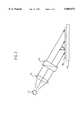
- FIG. 3is a view showing a first embodiment of the UV light irradiating apparatus consistent with the present invention.
- FIG. 4ais a plan view showing the spot of the UV light irradiated into the alignment layer when the UV light irradiating apparatus of FIG. 3 is used.
- FIG. 4bis a graph showing a photo-energy amount according to the alignment layer area of FIG. 4a.
- FIG. 5is a view showing a second embodiment of the UV light irradiating apparatus consistent with the present invention.
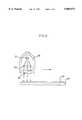
- FIG. 6ais a plan view showing the exposed area of the UV light irradiated into the alignment layer when the UV light irradiating apparatus of FIG. 5 is used.
- FIG. 6bis a graph showing a photo-energy amount according to the alignment layer area of FIG. 6a.
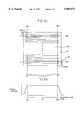
- FIG. 3is a view showing a first embodiment consistent with the present invention.
- the UV lightis generated from a UV lamp 11, such as a Hg lamp, and focused by a lens 12.
- This focused UV lightis polarized by a polarizer 13 and irradiated to a substrate 14 on which a photo-reacting alignment layer 15, which includes polysiloxane, is coated.
- the UV lamp 11, the lens 12, and the polarizer 13are arranged in a line and they are slanted at an angle ⁇ with respect to the substrate 14.
- the alignment layer 15 coated on the substrate 14is exposed with elliptical spot 16 of light as shown in FIG. 4a. Therefore, the exposed area 16 in the alignment layer 15 is larger than conventional area 6 as shown in FIG. 2a in accordance with the slanted angle ⁇ . To get the larger exposed area 16, the irradiation direction is more slanted against the alignment layer 15.
- ⁇ S ⁇refers to a range where the UV lamp 11 irradiates a uniform photo-energy amount
- ⁇ A ⁇refers to a range of alignment layer 15.
- the range corresponding to light spot Scovers the alignment layer range A. Therefore, the elliptical spot S having uniform photo-energy exposes the whole alignment layer range A, the spot S being larger than the conventional circle light spot.
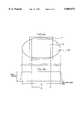
- FIG. 5is a view showing a second embodiment consistent with the present invention.
- a UV lamp 21, a lens 22, and a polarizer 23are mounted into a casing 20.
- a scan motor(not shown) moves the casing 20 above a substrate 24 coated with photo-reacting alignment layer 25 to scan the whole area of the alignment layer 25. Therefore, the whole area of the substrate is uniformly exposed by the moving UV light and given a uniform photo-energy amount, so that a pretilt determined on the alignment layer is uniform.
- FIG. 6aOne method for scanning the UV light into the alignment layer 25 is shown in FIG. 6a. If the irradiating direction is in the perpendicular direction to the substrate, the light spot 26 is circular. However, the irradiation direction may be oblique to the substrate.
- the start spot S x1y1 for irradiating UV lightis a tangent between extension lines from a first horizontal line S x1 , and a first vertical line S yl of the alignment layer 25.
- the end spot S xnyn for irradiating UV lightis a tangent between extension lines from a last horizontal line S xn and a last vertical line S yn of the alignment layer 25.
- the light spot 26begins moving from start spot S xlyl along the first horizontal line S xl until it contacts outside the last vertical line S yn . Then, the light spot 26 moves down along the last vertical line S yn in an interval retaining beam uniformity, such as 5 mm. In the second line S x2 , the spot moves in the reverse direction to the previous moving direction. The light spot 26 of UV light continuously moves until it meets the last spot S xnyn in the last horizontal line S xn . Thereby, every area in the alignment layer 25 is exposed with the same amount of UV light from light spot 26.
- the photo-energy absorbed into the range A of the alignment layer 25is uniform, as shown in FIG. 6b, because the spot is overlapped in the same times by the movement of the scan motor. Thereby, a large size liquid crystal display can be fabricated.
- unpolarized lightcan be adopted simply by removing a polarizer from the irradiating apparatus.
- the polarizercan be rotated for each corresponding domain.
- a domain of the alignment layer 15has its own pretilt by which a UV light, having a different polarization direction, is irradiated just into a certain domain using the mask.
- the other domainis also exposed by the UV light having a different polarization direction from the initially irradiated UV light by rotating the polarizer.
- the multi-domain liquid crystal cellsuch as two-domain or four-domain liquid crystal cell, etc, can be obtained.
- the UV lightsince the UV light obliquely irradiates into the alignment layer and/or scans the whole area of the alignment layer, a wider area of the alignment layer is uniformly exposed to the UV light.
- the substratemay be moved in a scanning motion relative to a stationary UV light source.
Landscapes
- Physics & Mathematics (AREA)
- Nonlinear Science (AREA)
- Spectroscopy & Molecular Physics (AREA)
- Mathematical Physics (AREA)
- Chemical & Material Sciences (AREA)
- Crystallography & Structural Chemistry (AREA)
- General Physics & Mathematics (AREA)
- Optics & Photonics (AREA)
- Liquid Crystal (AREA)
Abstract
Description
Claims (21)
Priority Applications (2)
| Application Number | Priority Date | Filing Date | Title |
|---|---|---|---|
| PCT/US1997/015530WO1998010278A1 (en) | 1996-09-09 | 1997-09-03 | Improved acoustic strain gauge and assembly and method for measuring strain |
| AU42489/97AAU4248997A (en) | 1996-09-09 | 1997-09-03 | Improved acoustic strain gauge and assembly and method for measuring strain |
Applications Claiming Priority (4)
| Application Number | Priority Date | Filing Date | Title |
|---|---|---|---|
| KR19962463 | 1996-02-01 | ||
| KR1019960002463AKR0169063B1 (en) | 1996-02-01 | 1996-02-01 | UV irradiation device for photo-alignment |
| KR199637076 | 1996-08-30 | ||
| KR1019960037076AKR100191135B1 (en) | 1996-08-30 | 1996-08-30 | Light irradiation method |
Publications (1)
| Publication Number | Publication Date |
|---|---|
| US5889571Atrue US5889571A (en) | 1999-03-30 |
Family
ID=26631623
Family Applications (1)
| Application Number | Title | Priority Date | Filing Date |
|---|---|---|---|
| US08/792,265Expired - LifetimeUS5889571A (en) | 1996-02-01 | 1997-01-31 | Ultraviolet irradiating device for photo-alignment process and an irradiating method using the same |
Country Status (5)
| Country | Link |
|---|---|
| US (1) | US5889571A (en) |
| JP (1) | JPH09211465A (en) |
| DE (1) | DE19703682B9 (en) |
| FR (1) | FR2744536B1 (en) |
| GB (1) | GB2309794B (en) |
Cited By (37)
| Publication number | Priority date | Publication date | Assignee | Title |
|---|---|---|---|---|
| US6020946A (en)* | 1998-02-23 | 2000-02-01 | International Business Machines Corporation | Dry processing for liquid-crystal displays using low energy ion bombardment |
| US6184959B1 (en)* | 1997-10-24 | 2001-02-06 | Sharp Kabushiki Kaisha | Liquid crystal display device having alignment film that provides alignment upon irradiation and manufacturing method the same |
| US6184958B1 (en)* | 1996-09-25 | 2001-02-06 | Hyundai Electronics Industries Co., Ltd. | Method of aligning an optically active compound contained in a polymer film on a substrate |
| US6191836B1 (en)* | 1996-11-07 | 2001-02-20 | Lg Philips Lcd, Co., Ltd. | Method for fabricating a liquid crystal cell |
| US6206527B1 (en) | 1998-11-24 | 2001-03-27 | Ushiodenki Kabushiki Kaisha | Device for oblique light irradiation |
| US6226066B1 (en) | 1996-01-09 | 2001-05-01 | Lg. Philips Lcd Co., Ltd. | Method for controlling pretilt angle direction in a liquid crystal cell |
| US6252642B1 (en)* | 1997-06-30 | 2001-06-26 | Hyundai Electronics Industries Co., Ltd. | Method for aligning polymer film and method for aligning liquid crystal by using polymer aligned-film |
| US6292296B1 (en)* | 1997-05-28 | 2001-09-18 | Lg. Philips Lcd Co., Ltd. | Large scale polarizer and polarizer system employing it |
| US20020039160A1 (en)* | 2000-10-04 | 2002-04-04 | Lg Philips Lcd Co., Ltd. | Liquid crystal display device and method for manufacturing the same |
| US6383579B1 (en) | 1999-04-21 | 2002-05-07 | Lg. Philips Lcd Co., Ltd. | Liquid crystal display device |
| US6399165B1 (en) | 1997-11-21 | 2002-06-04 | Lg. Philips Lcd Co., Ltd. | Liquid crystal display device |
| US6479218B1 (en) | 1999-10-14 | 2002-11-12 | Lg Philips Lcd Co., Ltd | Method for manufacturing multi-domain liquid crystal cell |
| US20030147032A1 (en)* | 2002-02-07 | 2003-08-07 | Park Moo Yeol | Ultraviolet irradiating device and method of manufacturing liquid crystal display device using the same |
| US20040051875A1 (en)* | 2002-09-12 | 2004-03-18 | Eastman Kodak Company | Method and system for fabricating optical film using an exposure source and reflecting surface |
| US6764724B1 (en) | 1999-03-25 | 2004-07-20 | Lg.Philips Lcd Co., Ltd. | Alignment layer for a liquid crystal display device |
| US6770335B2 (en) | 2000-10-28 | 2004-08-03 | Lg.Philips Lcd Co., Ltd. | Photoalignment materials and liquid crystal display device and method for fabricating the same with said materials |
| US6793987B2 (en) | 2000-10-28 | 2004-09-21 | Lg.Philips Lcd Co., Ltd. | Photoalignment materials and liquid crystal display fabricated with such photoalignment materials |
| US20040212790A1 (en)* | 2003-04-24 | 2004-10-28 | Eastman Kodak Company | Optical exposure apparatus for forming an alignment layer |
| US20050140885A1 (en)* | 2002-07-12 | 2005-06-30 | Leidig Carl F. | Optical exposure apparatus and method for aligning a substrate |
| US20050259203A1 (en)* | 2002-03-29 | 2005-11-24 | Jsr Corporation | Optical alignment method and liquid crystal display element |
| US20050270617A1 (en)* | 2004-06-02 | 2005-12-08 | Solomon Jeffrey L | Polarized UV exposure system |
| US20060057306A1 (en)* | 2004-09-16 | 2006-03-16 | Ushiodenki Kabushiki Kaisha | Process for optical alignment |
| US7061679B1 (en) | 1998-05-27 | 2006-06-13 | Lg. Philips Lcd Co., Ltd. | Light irradiating device |
| US20060128555A1 (en)* | 1999-09-07 | 2006-06-15 | Zhiping Shan | Novel zeolite composite, method for making and catalytic application thereof |
| US20070247506A1 (en)* | 2006-04-25 | 2007-10-25 | Ushiodenki Kabushiki Kaisha | Light irradiation apparatus and injet printer |
| US20080074586A1 (en)* | 1998-08-03 | 2008-03-27 | Michiaki Sakamoto | Liquid crystal display device and method of manufacturing the same |
| US7365817B2 (en)* | 2000-10-04 | 2008-04-29 | Lg.Philips Lcd Co., Ltd. | Multi-domain liquid crystal display and method for manufacturing the same |
| US20080309863A1 (en)* | 1997-02-27 | 2008-12-18 | Sharp Kabushiki Kaisha | Alignment treatment of liquid crystal display device |
| US8064019B2 (en) | 2005-12-02 | 2011-11-22 | Sharp Kabushiki Kaisha | Production method of liquid crystal display including scanning exposure |
| EP2584400A1 (en)* | 2011-10-20 | 2013-04-24 | Samsung Display Co., Ltd. | Liquid crystal display device, alignment film, and method for manufacturing the same |
| US20140360860A1 (en)* | 2011-08-29 | 2014-12-11 | Sharp Kabushiki Kaisha | Method for manufacturing liquid crystal display device |
| US20150037510A1 (en)* | 2013-08-01 | 2015-02-05 | Far Eastern New Century Corporation | Method of manufacturing a retardation film |
| CN104375229A (en)* | 2013-08-14 | 2015-02-25 | 远东新世纪股份有限公司 | Manufacturing method of retardation film |
| CN105044989A (en)* | 2015-08-31 | 2015-11-11 | 武汉华星光电技术有限公司 | Manufacture method and system for alignment film |
| CN109212837A (en)* | 2017-06-30 | 2019-01-15 | 上海微电子装备(集团)股份有限公司 | A kind of smooth alignment apparatus and method |
| WO2021151846A1 (en) | 2020-01-29 | 2021-08-05 | Merck Patent Gmbh | Method for adjustment of alignment of liquid crystals |
| US20250053047A1 (en)* | 2021-12-23 | 2025-02-13 | Osaka University | Liquid crystal element and liquid crystal element production method |
Families Citing this family (10)
| Publication number | Priority date | Publication date | Assignee | Title |
|---|---|---|---|---|
| TW536644B (en) | 1997-10-29 | 2003-06-11 | Ushio Electric Inc | Polarized light radiation device for alignment film of liquid crystal display element |
| KR100323731B1 (en)* | 1998-11-06 | 2002-05-09 | 구본준, 론 위라하디락사 | Light irradiating device |
| US6532047B1 (en) | 1998-10-27 | 2003-03-11 | Ushiodenki Kabushiki Kaisha | Irradiation device for polarized light for optical alignment of a liquid crystal cell element |
| JP3384346B2 (en)* | 1999-01-14 | 2003-03-10 | ウシオ電機株式会社 | Polarized light irradiation device for photo alignment of liquid crystal display devices |
| JP3844234B2 (en)* | 2002-10-25 | 2006-11-08 | Jsr株式会社 | Photo-alignment method and liquid crystal display element |
| JP3804934B2 (en)* | 2002-03-29 | 2006-08-02 | Jsr株式会社 | Photo-alignment method |
| US7244627B2 (en)* | 2003-08-25 | 2007-07-17 | Lg.Philips Lcd Co., Ltd. | Method for fabricating liquid crystal display device |
| JP4383825B2 (en)* | 2003-10-27 | 2009-12-16 | 株式会社 日立ディスプレイズ | Liquid crystal display |
| DK1970734T3 (en)* | 2007-03-12 | 2012-01-16 | Jds Uniphase Corp | Process for producing a spacer wavy plate with liquid crystals |
| JP6201707B2 (en)* | 2013-12-11 | 2017-09-27 | 東芝ライテック株式会社 | UV irradiation equipment |
Citations (14)
| Publication number | Priority date | Publication date | Assignee | Title |
|---|---|---|---|---|
| GB1489816A (en)* | 1975-12-12 | 1977-10-26 | Marconi Co Ltd | Apparatus for producing linear movement |
| GB2046928A (en)* | 1979-04-11 | 1980-11-19 | Gerber Scientific Instr Co | Photodrafting |
| GB2215477A (en)* | 1988-03-01 | 1989-09-20 | Ferranti Plc | Apparatus for use in producing a multiple image mask to be employed in photolithographic processing |
| EP0491368A2 (en)* | 1990-12-18 | 1992-06-24 | R.R. Donnelly & Sons Company | Method and apparatus for making print imaging media |
| EP0632311A1 (en)* | 1993-06-29 | 1995-01-04 | Stanley Electric Co., Ltd. | Method of orienting liquid crystal molecules in a multi-domain liquid crystal display cell |
| GB2281977A (en)* | 1993-09-18 | 1995-03-22 | Gold Star Co | Orientation film for a liquid crystal display |
| GB2286893A (en)* | 1994-02-09 | 1995-08-30 | Secr Defence | Liquid crystal alignment |
| GB2286894A (en)* | 1994-02-09 | 1995-08-30 | Secr Defence | Liquid crystal alignment |
| EP0742471A2 (en)* | 1995-05-10 | 1996-11-13 | Stanley Electric Co., Ltd. | Arrangement for rubbingless orientation of liquid crystals with tilt |
| US5576862A (en)* | 1993-06-29 | 1996-11-19 | Stanley Electric Co., Ltd. | Positive orientations of liquid crystal molecules in a multi-domain liquid crystal display cell |
| EP0750212A2 (en)* | 1995-06-22 | 1996-12-27 | International Business Machines Corporation | Liquid crystal display device |
| US5604615A (en)* | 1994-05-27 | 1997-02-18 | Sharp Kabushiki Kaisha | Liquid crystal display device and methods for producing same with alignment layer having new bond formation or bond cleavage reaction of molecular chains by light irradiation |
| US5623354A (en)* | 1994-02-10 | 1997-04-22 | International Business Machines Corporation | Liquid crystal display with multi-domains |
| US5657105A (en)* | 1994-01-10 | 1997-08-12 | Honeywell Inc. | Multi-domain liquid crystal displays |
Family Cites Families (5)
| Publication number | Priority date | Publication date | Assignee | Title |
|---|---|---|---|---|
| JPS60147757A (en)* | 1984-01-11 | 1985-08-03 | Canon Inc | A device that exposes an image to a photoreceptor |
| JPS6327815A (en)* | 1986-07-22 | 1988-02-05 | Victor Co Of Japan Ltd | Manufacture of liquid crystal element |
| EP0525478B1 (en)* | 1991-07-26 | 1997-06-11 | F. Hoffmann-La Roche Ag | Liquid crystal display cell |
| JPH07239475A (en)* | 1994-02-25 | 1995-09-12 | Matsushita Electric Ind Co Ltd | Liquid crystal molecule alignment method |
| KR0181782B1 (en)* | 1995-12-08 | 1999-05-01 | 구자홍 | Bend-oriented liquid crystal cell manufacturing method using light |
- 1997
- 1997-01-31FRFR9701084Apatent/FR2744536B1/ennot_activeExpired - Lifetime
- 1997-01-31DEDE19703682Apatent/DE19703682B9/ennot_activeExpired - Lifetime
- 1997-01-31USUS08/792,265patent/US5889571A/ennot_activeExpired - Lifetime
- 1997-01-31GBGB9702048Apatent/GB2309794B/ennot_activeExpired - Lifetime
- 1997-02-03JPJP9020509Apatent/JPH09211465A/enactivePending
Patent Citations (15)
| Publication number | Priority date | Publication date | Assignee | Title |
|---|---|---|---|---|
| GB1489816A (en)* | 1975-12-12 | 1977-10-26 | Marconi Co Ltd | Apparatus for producing linear movement |
| GB2046928A (en)* | 1979-04-11 | 1980-11-19 | Gerber Scientific Instr Co | Photodrafting |
| GB2215477A (en)* | 1988-03-01 | 1989-09-20 | Ferranti Plc | Apparatus for use in producing a multiple image mask to be employed in photolithographic processing |
| EP0491368A2 (en)* | 1990-12-18 | 1992-06-24 | R.R. Donnelly & Sons Company | Method and apparatus for making print imaging media |
| US5576862A (en)* | 1993-06-29 | 1996-11-19 | Stanley Electric Co., Ltd. | Positive orientations of liquid crystal molecules in a multi-domain liquid crystal display cell |
| EP0632311A1 (en)* | 1993-06-29 | 1995-01-04 | Stanley Electric Co., Ltd. | Method of orienting liquid crystal molecules in a multi-domain liquid crystal display cell |
| GB2281977A (en)* | 1993-09-18 | 1995-03-22 | Gold Star Co | Orientation film for a liquid crystal display |
| US5464669A (en)* | 1993-09-18 | 1995-11-07 | Goldstar Co., Ltd. | Method for forming an orientation film of photopolymer in a liquid crystal display |
| US5657105A (en)* | 1994-01-10 | 1997-08-12 | Honeywell Inc. | Multi-domain liquid crystal displays |
| GB2286893A (en)* | 1994-02-09 | 1995-08-30 | Secr Defence | Liquid crystal alignment |
| GB2286894A (en)* | 1994-02-09 | 1995-08-30 | Secr Defence | Liquid crystal alignment |
| US5623354A (en)* | 1994-02-10 | 1997-04-22 | International Business Machines Corporation | Liquid crystal display with multi-domains |
| US5604615A (en)* | 1994-05-27 | 1997-02-18 | Sharp Kabushiki Kaisha | Liquid crystal display device and methods for producing same with alignment layer having new bond formation or bond cleavage reaction of molecular chains by light irradiation |
| EP0742471A2 (en)* | 1995-05-10 | 1996-11-13 | Stanley Electric Co., Ltd. | Arrangement for rubbingless orientation of liquid crystals with tilt |
| EP0750212A2 (en)* | 1995-06-22 | 1996-12-27 | International Business Machines Corporation | Liquid crystal display device |
Non-Patent Citations (4)
| Title |
|---|
| M. Schadt et al. "Surface-Induced parallel Alignment of Liquid Crystals by Linearly Polymerized Photopolymers", Jpn. J. Appl. Phys. vol. 31(1992) part 1, No 7, Jul. 1992, pp. 2155-2164. |
| M. Schadt et al. Surface Induced parallel Alignment of Liquid Crystals by Linearly Polymerized Photopolymers , Jpn. J. Appl. Phys. vol. 31(1992) part 1, No 7, Jul. 1992, pp. 2155 2164.* |
| T. Hashimoto et al. "TN-LCD with Quartered Subpixels Using Polarized UV-Light-Irradiated Polymer Orientation Films", (SID 95 Digest) pp. 877-880. |
| T. Hashimoto et al. TN LCD with Quartered Subpixels Using Polarized UV Light Irradiated Polymer Orientation Films , (SID 95 Digest) pp. 877 880.* |
Cited By (95)
| Publication number | Priority date | Publication date | Assignee | Title |
|---|---|---|---|---|
| US6633355B2 (en) | 1996-01-09 | 2003-10-14 | Lg. Philips Lcd Co., Ltd. | Method for controlling pretilt angle direction in a liquid crystal cell |
| US7145618B2 (en) | 1996-01-09 | 2006-12-05 | Lg.Philips Lcd Co., Ltd | Method for controlling pretilt angle direction in a liquid crystal cell |
| US6226066B1 (en) | 1996-01-09 | 2001-05-01 | Lg. Philips Lcd Co., Ltd. | Method for controlling pretilt angle direction in a liquid crystal cell |
| US6879363B2 (en) | 1996-01-09 | 2005-04-12 | Lg.Philips Lcd Co., Ltd. | Method for controlling pretilt angle direction in a liquid crystal cell |
| US6433850B2 (en) | 1996-01-09 | 2002-08-13 | Lg. Phillips Lcd Co., Ltd. | Pretilt angle direction in a liquid crystal cell |
| US6184958B1 (en)* | 1996-09-25 | 2001-02-06 | Hyundai Electronics Industries Co., Ltd. | Method of aligning an optically active compound contained in a polymer film on a substrate |
| US6721025B2 (en) | 1996-11-07 | 2004-04-13 | Lg.Philips Lcd Co., Ltd | Method for fabricating a liquid crystal cell |
| US6191836B1 (en)* | 1996-11-07 | 2001-02-20 | Lg Philips Lcd, Co., Ltd. | Method for fabricating a liquid crystal cell |
| US6462797B1 (en) | 1996-11-07 | 2002-10-08 | Lg. Philips Lcd Co., Ltd. | Method for fabricating a liquid crystal cell |
| US6417905B1 (en) | 1996-11-07 | 2002-07-09 | Lg. Philips Lcd Co., Ltd. | Method for fabricating a liquid crystal cell |
| US7916256B2 (en) | 1997-02-27 | 2011-03-29 | Sharp Kabushiki Kaisha | Liquid crystal display device |
| US20080309863A1 (en)* | 1997-02-27 | 2008-12-18 | Sharp Kabushiki Kaisha | Alignment treatment of liquid crystal display device |
| US8767155B2 (en) | 1997-02-27 | 2014-07-01 | Sharp Kabushiki Kaisha | Method for producing liquid crystal display device |
| US20080309862A1 (en)* | 1997-02-27 | 2008-12-18 | Sharp Kabushiki Kaisha | Alignment treatment of liquid crystal display device |
| US20080316408A1 (en)* | 1997-02-27 | 2008-12-25 | Sharp Kabushiki Kaisha | Alignment treatment of liquid crystal display device |
| US8085374B2 (en) | 1997-02-27 | 2011-12-27 | Sharp Kabushiki Kaisha | Alignment treatment of liquid crystal display device |
| US20080316409A1 (en)* | 1997-02-27 | 2008-12-25 | Sharp Kabushiki Kaisha | Alignment treatment of liquid crystal display device |
| US8120737B2 (en) | 1997-02-27 | 2012-02-21 | Sharp Kabushiki Kaisha | Alignment treatment of liquid crystal display device |
| US7768622B2 (en) | 1997-02-27 | 2010-08-03 | Sharp Kabushiki Kaisha | Alignment treatment of liquid crystal display device |
| US7924381B2 (en) | 1997-02-27 | 2011-04-12 | Sharp Kabushiki Kaisha | Method for producing liquid crystal display device |
| US8054425B2 (en) | 1997-02-27 | 2011-11-08 | Sharp Kabushiki Kaisha | Alignment treatment of liquid crystal display device |
| US6292296B1 (en)* | 1997-05-28 | 2001-09-18 | Lg. Philips Lcd Co., Ltd. | Large scale polarizer and polarizer system employing it |
| US7016112B2 (en) | 1997-05-28 | 2006-03-21 | Lg.Philips Lcd Co., Ltd. | Large scale polarizer and polarizer system employing it |
| US6639720B2 (en) | 1997-05-28 | 2003-10-28 | Lg.Philips Lcd Co., Ltd. | Large scale polarizer and polarizer system employing it |
| US7016113B2 (en) | 1997-05-28 | 2006-03-21 | Lg.Philips Lcd Co., Ltd. | Large scale polarizer and polarizer system employing it |
| US7911696B1 (en) | 1997-05-28 | 2011-03-22 | Lg Display Co., Ltd. | Large scale polarizer and polarizer system employing it |
| US6252642B1 (en)* | 1997-06-30 | 2001-06-26 | Hyundai Electronics Industries Co., Ltd. | Method for aligning polymer film and method for aligning liquid crystal by using polymer aligned-film |
| US6184959B1 (en)* | 1997-10-24 | 2001-02-06 | Sharp Kabushiki Kaisha | Liquid crystal display device having alignment film that provides alignment upon irradiation and manufacturing method the same |
| US6572939B2 (en) | 1997-11-21 | 2003-06-03 | Lg.Philips Lcd Co., Ltd. | Liquid crystal display device |
| US6399165B1 (en) | 1997-11-21 | 2002-06-04 | Lg. Philips Lcd Co., Ltd. | Liquid crystal display device |
| US6020946A (en)* | 1998-02-23 | 2000-02-01 | International Business Machines Corporation | Dry processing for liquid-crystal displays using low energy ion bombardment |
| US7061679B1 (en) | 1998-05-27 | 2006-06-13 | Lg. Philips Lcd Co., Ltd. | Light irradiating device |
| US7561238B2 (en) | 1998-08-03 | 2009-07-14 | Nec Lcd Technologies, Ltd. | Liquid crystal display device and method of manufacturing the same |
| US20080074586A1 (en)* | 1998-08-03 | 2008-03-27 | Michiaki Sakamoto | Liquid crystal display device and method of manufacturing the same |
| US6206527B1 (en) | 1998-11-24 | 2001-03-27 | Ushiodenki Kabushiki Kaisha | Device for oblique light irradiation |
| US7608211B2 (en) | 1999-03-25 | 2009-10-27 | Lg Display Co., Ltd. | Method of making a liquid crystal display device |
| US20100009069A1 (en)* | 1999-03-25 | 2010-01-14 | Mi Sook Nam | Method of forming an alignment layer for liquid crystal display device |
| US7901605B2 (en) | 1999-03-25 | 2011-03-08 | Lg Display Co., Ltd. | Method of forming an alignment layer for liquid crystal display device |
| US20040213924A1 (en)* | 1999-03-25 | 2004-10-28 | Nam Mi Sook | Alignment layer for a liquid crystal display device |
| US6764724B1 (en) | 1999-03-25 | 2004-07-20 | Lg.Philips Lcd Co., Ltd. | Alignment layer for a liquid crystal display device |
| US7014892B2 (en) | 1999-03-25 | 2006-03-21 | Lg.Philips Lcd Co., Ltd. | Alignment layer for a liquid crystal display device |
| US6582784B2 (en) | 1999-04-21 | 2003-06-24 | Lg.Philips Lcd Co., Ltd. | Liquid crystal display |
| US6383579B1 (en) | 1999-04-21 | 2002-05-07 | Lg. Philips Lcd Co., Ltd. | Liquid crystal display device |
| US20060128555A1 (en)* | 1999-09-07 | 2006-06-15 | Zhiping Shan | Novel zeolite composite, method for making and catalytic application thereof |
| US6787292B2 (en) | 1999-10-14 | 2004-09-07 | Lg.Philips Lcd Co., Ltd. | Method for manufacturing multi-domain liquid crystal cell |
| US6479218B1 (en) | 1999-10-14 | 2002-11-12 | Lg Philips Lcd Co., Ltd | Method for manufacturing multi-domain liquid crystal cell |
| US20020039160A1 (en)* | 2000-10-04 | 2002-04-04 | Lg Philips Lcd Co., Ltd. | Liquid crystal display device and method for manufacturing the same |
| US7365817B2 (en)* | 2000-10-04 | 2008-04-29 | Lg.Philips Lcd Co., Ltd. | Multi-domain liquid crystal display and method for manufacturing the same |
| US7429412B2 (en)* | 2000-10-04 | 2008-09-30 | Lg Display Co., Ltd. | Liquid crystal display device and method for manufacturing the same |
| US6770335B2 (en) | 2000-10-28 | 2004-08-03 | Lg.Philips Lcd Co., Ltd. | Photoalignment materials and liquid crystal display device and method for fabricating the same with said materials |
| US20040219307A1 (en)* | 2000-10-28 | 2004-11-04 | Shin Hyun Ho | Photoalignment materials and liquid crystal display fabricated with such photoalignment materials |
| US7083833B2 (en) | 2000-10-28 | 2006-08-01 | Lg.Philips Lcd Co., Ltd. | Photoalignment materials and liquid crystal display fabricated with such photoalignment materials |
| US6793987B2 (en) | 2000-10-28 | 2004-09-21 | Lg.Philips Lcd Co., Ltd. | Photoalignment materials and liquid crystal display fabricated with such photoalignment materials |
| US20030147032A1 (en)* | 2002-02-07 | 2003-08-07 | Park Moo Yeol | Ultraviolet irradiating device and method of manufacturing liquid crystal display device using the same |
| US7349050B2 (en)* | 2002-02-07 | 2008-03-25 | Lg.Philips Lcd Co., Ltd. | Ultraviolet irradiating device and method of manufacturing liquid crystal display device using the same |
| US20050259203A1 (en)* | 2002-03-29 | 2005-11-24 | Jsr Corporation | Optical alignment method and liquid crystal display element |
| US7787085B2 (en) | 2002-03-29 | 2010-08-31 | Jsr Corporation | Optical alignment method and liquid crystal display element |
| US20080123046A1 (en)* | 2002-03-29 | 2008-05-29 | Jsr Corporation | Optical alignment method and liquid crystal display element |
| KR100961323B1 (en) | 2002-03-29 | 2010-06-04 | 제이에스알 가부시끼가이샤 | Photo-alignment method and liquid crystal display device |
| US6988811B2 (en) | 2002-07-12 | 2006-01-24 | Eastman Kodak Company | Optical exposure apparatus and method for aligning a substrate |
| US20050140885A1 (en)* | 2002-07-12 | 2005-06-30 | Leidig Carl F. | Optical exposure apparatus and method for aligning a substrate |
| US20040051875A1 (en)* | 2002-09-12 | 2004-03-18 | Eastman Kodak Company | Method and system for fabricating optical film using an exposure source and reflecting surface |
| US6943930B2 (en) | 2002-09-12 | 2005-09-13 | Eastman Kodak Company | Method and system for fabricating optical film using an exposure source and reflecting surface |
| US20040212790A1 (en)* | 2003-04-24 | 2004-10-28 | Eastman Kodak Company | Optical exposure apparatus for forming an alignment layer |
| US6844913B2 (en) | 2003-04-24 | 2005-01-18 | Eastman Kodak Company | Optical exposure apparatus for forming an alignment layer |
| US20050270617A1 (en)* | 2004-06-02 | 2005-12-08 | Solomon Jeffrey L | Polarized UV exposure system |
| US7413317B2 (en) | 2004-06-02 | 2008-08-19 | 3M Innovative Properties Company | Polarized UV exposure system |
| US20060057306A1 (en)* | 2004-09-16 | 2006-03-16 | Ushiodenki Kabushiki Kaisha | Process for optical alignment |
| US7507448B2 (en) | 2004-09-16 | 2009-03-24 | Ushiodenki Kabushiki Kaisha | Process for optical alignment |
| CN100451772C (en)* | 2004-09-16 | 2009-01-14 | 优志旺电机株式会社 | photo-alignment method |
| US8427611B2 (en)* | 2005-12-02 | 2013-04-23 | Sharp Kabushiki Kaisha | Production method of liquid crystal display including scanning exposure |
| CN102226860B (en)* | 2005-12-02 | 2013-04-10 | 夏普株式会社 | Production method of liquid crystal display and exposure device for alignment treatment |
| US8130348B2 (en) | 2005-12-02 | 2012-03-06 | Sharp Kabushiki Kaisha | Production method of liquid crystal display including scanning exposure |
| US8199294B2 (en)* | 2005-12-02 | 2012-06-12 | Sharp Kabushiki Kaisha | Production method of liquid crystal display including scanning exposure |
| CN101322067B (en)* | 2005-12-02 | 2012-08-22 | 夏普株式会社 | Manufacturing method of liquid crystal display device and exposure device for alignment treatment |
| US20120287389A1 (en)* | 2005-12-02 | 2012-11-15 | Sharp Kabushiki Kaisha | Production method of liquid crystal display including scanning exposure |
| CN102226856B (en)* | 2005-12-02 | 2013-03-13 | 夏普株式会社 | Production method of liquid crystal display and exposure device for alignment treatment |
| TWI474088B (en)* | 2005-12-02 | 2015-02-21 | Sharp Kk | Production method of liquid crystal display and exposure device for alignment treatment |
| TWI456317B (en)* | 2005-12-02 | 2014-10-11 | Sharp Kk | Production method of liquid crystal display and exposure device for alignment treatment |
| US8064019B2 (en) | 2005-12-02 | 2011-11-22 | Sharp Kabushiki Kaisha | Production method of liquid crystal display including scanning exposure |
| US20070247506A1 (en)* | 2006-04-25 | 2007-10-25 | Ushiodenki Kabushiki Kaisha | Light irradiation apparatus and injet printer |
| US7963647B2 (en)* | 2006-04-25 | 2011-06-21 | Ushiodenki Kabushiki Kaisha | Light irradiation apparatus and injet printer |
| US20140360860A1 (en)* | 2011-08-29 | 2014-12-11 | Sharp Kabushiki Kaisha | Method for manufacturing liquid crystal display device |
| US9249242B2 (en)* | 2011-08-29 | 2016-02-02 | Sharp Kabushiki Kaisha | Method for manufacturing liquid crystal display device |
| US9723769B2 (en) | 2011-10-20 | 2017-08-01 | Samsung Display Co., Ltd. | Liquid crystal display device, alignment film, and methods for manufacturing the same |
| US8962106B2 (en) | 2011-10-20 | 2015-02-24 | Samsung Display Co., Ltd. | Liquid crystal display device, alignment film, and methods for manufacturing the same |
| EP2584400A1 (en)* | 2011-10-20 | 2013-04-24 | Samsung Display Co., Ltd. | Liquid crystal display device, alignment film, and method for manufacturing the same |
| US20150037510A1 (en)* | 2013-08-01 | 2015-02-05 | Far Eastern New Century Corporation | Method of manufacturing a retardation film |
| CN104375229A (en)* | 2013-08-14 | 2015-02-25 | 远东新世纪股份有限公司 | Manufacturing method of retardation film |
| CN105044989A (en)* | 2015-08-31 | 2015-11-11 | 武汉华星光电技术有限公司 | Manufacture method and system for alignment film |
| CN105044989B (en)* | 2015-08-31 | 2018-02-16 | 武汉华星光电技术有限公司 | The preparation method and system of a kind of alignment film |
| CN109212837A (en)* | 2017-06-30 | 2019-01-15 | 上海微电子装备(集团)股份有限公司 | A kind of smooth alignment apparatus and method |
| CN109212837B (en)* | 2017-06-30 | 2021-04-09 | 上海微电子装备(集团)股份有限公司 | Optical alignment device and method |
| WO2021151846A1 (en) | 2020-01-29 | 2021-08-05 | Merck Patent Gmbh | Method for adjustment of alignment of liquid crystals |
| US20250053047A1 (en)* | 2021-12-23 | 2025-02-13 | Osaka University | Liquid crystal element and liquid crystal element production method |
Also Published As
| Publication number | Publication date |
|---|---|
| GB2309794A (en) | 1997-08-06 |
| DE19703682B9 (en) | 2006-11-23 |
| GB2309794B (en) | 1998-07-15 |
| DE19703682B4 (en) | 2006-08-10 |
| JPH09211465A (en) | 1997-08-15 |
| GB9702048D0 (en) | 1997-03-19 |
| DE19703682A1 (en) | 1997-08-07 |
| FR2744536B1 (en) | 2004-03-05 |
| FR2744536A1 (en) | 1997-08-08 |
Similar Documents
| Publication | Publication Date | Title |
|---|---|---|
| US5889571A (en) | Ultraviolet irradiating device for photo-alignment process and an irradiating method using the same | |
| JP3075917B2 (en) | Liquid crystal display device, its manufacturing method and its manufacturing device | |
| US5853818A (en) | Method for manufacturing multi-domain liquid crystal cell | |
| JP4754037B2 (en) | Manufacturing method of liquid crystal display device and aligner exposure apparatus | |
| JP3926874B2 (en) | Liquid crystal cell manufacturing method and liquid crystal cell | |
| JP4057106B2 (en) | Manufacturing method of multi-domain liquid crystal cell | |
| US6295110B1 (en) | Liquid crystal display device having orientation film oriented by light | |
| EP0996028A2 (en) | A liquid crystal display device and a method of manufacture thereof, and a substrate with alignment layer and a method of manufacture thereof | |
| KR100329695B1 (en) | Liquid crystal device alignment | |
| JPS60217343A (en) | Liquid crystal display device and its preparation | |
| JPS6060624A (en) | Liquid crystal display panel and its manufacturing method | |
| KR970076005A (en) | Orientation film processing method of liquid crystal display device for wide viewing angle | |
| JPH0756173A (en) | Liquid crystal display device, liquid crystal alignment treatment method, and liquid crystal display device manufacturing method | |
| JP2003334674A (en) | Laser beam machining method | |
| CN106918955A (en) | A kind of smooth alignment apparatus and method, liquid crystal display panel | |
| JPH05224206A (en) | Orientation treatment device and method for oriented film for liquid crystal | |
| KR0182415B1 (en) | Manufacturing method of substrate for liquid crystal display | |
| GB2314170A (en) | Alignment layers for liquid crystal devices | |
| KR100205260B1 (en) | Manufacturing method of liquid crystal cell using optical alignment | |
| JP3860872B2 (en) | Control method of alignment direction of liquid crystal cell | |
| KR100191135B1 (en) | Light irradiation method | |
| US6924860B2 (en) | Polarized UV light irradiation method for liquid crystal display device | |
| KR20030039401A (en) | A Display Device of Liquid Crystal On Silicone by Photo Alignment Technology And Method For Producing The Same | |
| KR100245052B1 (en) | Liquid crystal display alignment layer and method of processing alignment | |
| US9040229B2 (en) | Maskless process for pre-tilting liquid crystal molecules |
Legal Events
| Date | Code | Title | Description |
|---|---|---|---|
| AS | Assignment | Owner name:LG ELECTRONICS INC., KOREA, REPUBLIC OF Free format text:ASSIGNMENT OF ASSIGNORS INTEREST;ASSIGNORS:KIM, JONG HYUN;YOON, KI HYUK;WOO, JOUNG WON;AND OTHERS;REEL/FRAME:008530/0089 Effective date:19970130 | |
| FEPP | Fee payment procedure | Free format text:PAYOR NUMBER ASSIGNED (ORIGINAL EVENT CODE: ASPN); ENTITY STATUS OF PATENT OWNER: LARGE ENTITY | |
| STCF | Information on status: patent grant | Free format text:PATENTED CASE | |
| AS | Assignment | Owner name:LG. PHILIPS LCD CO., LTD., KOREA, DEMOCRATIC PEOPL Free format text:ASSIGNMENT OF ASSIGNORS INTEREST;ASSIGNOR:LG ELECTRONICS, INC.;REEL/FRAME:010281/0291 Effective date:19990921 | |
| FPAY | Fee payment | Year of fee payment:4 | |
| FPAY | Fee payment | Year of fee payment:8 | |
| AS | Assignment | Owner name:LG.PHILIPS LCD CO., LTD., KOREA, REPUBLIC OF Free format text:ASSIGNMENT OF ASSIGNORS INTEREST;ASSIGNOR:LG ELECTRONICS INC.;REEL/FRAME:020385/0124 Effective date:19990921 | |
| AS | Assignment | Owner name:LG DISPLAY CO., LTD., KOREA, REPUBLIC OF Free format text:CHANGE OF NAME;ASSIGNOR:LG. PHILIPS LCD CO., LTD.;REEL/FRAME:021301/0282 Effective date:20080229 | |
| FEPP | Fee payment procedure | Free format text:PAYER NUMBER DE-ASSIGNED (ORIGINAL EVENT CODE: RMPN); ENTITY STATUS OF PATENT OWNER: LARGE ENTITY Free format text:PAYOR NUMBER ASSIGNED (ORIGINAL EVENT CODE: ASPN); ENTITY STATUS OF PATENT OWNER: LARGE ENTITY | |
| FPAY | Fee payment | Year of fee payment:12 |