US5886866A - Electrostatic chuck having a combination electrode structure for substrate chucking, heating and biasing - Google Patents
Electrostatic chuck having a combination electrode structure for substrate chucking, heating and biasingDownload PDFInfo
- Publication number
- US5886866A US5886866AUS09/111,104US11110498AUS5886866AUS 5886866 AUS5886866 AUS 5886866AUS 11110498 AUS11110498 AUS 11110498AUS 5886866 AUS5886866 AUS 5886866A
- Authority
- US
- United States
- Prior art keywords
- electrode
- feedthroughs
- electrodes
- pair
- electrostatic chuck
- Prior art date
- Legal status (The legal status is an assumption and is not a legal conclusion. Google has not performed a legal analysis and makes no representation as to the accuracy of the status listed.)
- Expired - Lifetime
Links
- 238000010438heat treatmentMethods0.000titleclaimsabstractdescription37
- 239000000758substrateSubstances0.000titledescription5
- 229910010293ceramic materialInorganic materials0.000claimsabstractdescription14
- 239000004065semiconductorSubstances0.000claimsdescription16
- 239000003990capacitorSubstances0.000claimsdescription8
- 241001272720Medialuna californiensisSpecies0.000claimsdescription5
- ZOKXTWBITQBERF-UHFFFAOYSA-NMolybdenumChemical compound[Mo]ZOKXTWBITQBERF-UHFFFAOYSA-N0.000claimsdescription5
- 239000003989dielectric materialSubstances0.000claimsdescription5
- 229910052750molybdenumInorganic materials0.000claimsdescription5
- 239000011733molybdenumSubstances0.000claimsdescription5
- PMHQVHHXPFUNSP-UHFFFAOYSA-Mcopper(1+);methylsulfanylmethane;bromideChemical compoundBr[Cu].CSCPMHQVHHXPFUNSP-UHFFFAOYSA-M0.000claimsdescription3
- 230000009977dual effectEffects0.000claimsdescription3
- 238000005485electric heatingMethods0.000abstractdescription2
- 230000000717retained effectEffects0.000abstract1
- RTAQQCXQSZGOHL-UHFFFAOYSA-NTitaniumChemical group[Ti]RTAQQCXQSZGOHL-UHFFFAOYSA-N0.000description4
- NJPPVKZQTLUDBO-UHFFFAOYSA-NnovaluronChemical compoundC1=C(Cl)C(OC(F)(F)C(OC(F)(F)F)F)=CC=C1NC(=O)NC(=O)C1=C(F)C=CC=C1FNJPPVKZQTLUDBO-UHFFFAOYSA-N0.000description4
- 238000005240physical vapour depositionMethods0.000description4
- 239000010936titaniumSubstances0.000description4
- 229910052719titaniumInorganic materials0.000description4
- 230000005684electric fieldEffects0.000description3
- 239000007787solidSubstances0.000description3
- WYTGDNHDOZPMIW-RCBQFDQVSA-NalstonineNatural productsC1=CC2=C3C=CC=CC3=NC2=C2N1C[C@H]1[C@H](C)OC=C(C(=O)OC)[C@H]1C2WYTGDNHDOZPMIW-RCBQFDQVSA-N0.000description2
- 238000005229chemical vapour depositionMethods0.000description2
- 230000008878couplingEffects0.000description2
- 238000010168coupling processMethods0.000description2
- 238000005859coupling reactionMethods0.000description2
- 238000000151depositionMethods0.000description2
- 230000008021depositionEffects0.000description2
- 230000000694effectsEffects0.000description2
- 239000007772electrode materialSubstances0.000description2
- 230000020169heat generationEffects0.000description2
- 239000000463materialSubstances0.000description2
- WFKWXMTUELFFGS-UHFFFAOYSA-NtungstenChemical compound[W]WFKWXMTUELFFGS-UHFFFAOYSA-N0.000description2
- 229910052721tungstenInorganic materials0.000description2
- 239000010937tungstenSubstances0.000description2
- 238000005530etchingMethods0.000description1
- 229910052751metalInorganic materials0.000description1
- 239000002184metalSubstances0.000description1
- 238000000034methodMethods0.000description1
- 238000012986modificationMethods0.000description1
- 230000004048modificationEffects0.000description1
- 229910001220stainless steelInorganic materials0.000description1
- 239000010935stainless steelSubstances0.000description1
Images


Classifications
- H—ELECTRICITY
- H01—ELECTRIC ELEMENTS
- H01L—SEMICONDUCTOR DEVICES NOT COVERED BY CLASS H10
- H01L21/00—Processes or apparatus adapted for the manufacture or treatment of semiconductor or solid state devices or of parts thereof
- H01L21/67—Apparatus specially adapted for handling semiconductor or electric solid state devices during manufacture or treatment thereof; Apparatus specially adapted for handling wafers during manufacture or treatment of semiconductor or electric solid state devices or components ; Apparatus not specifically provided for elsewhere
- H01L21/683—Apparatus specially adapted for handling semiconductor or electric solid state devices during manufacture or treatment thereof; Apparatus specially adapted for handling wafers during manufacture or treatment of semiconductor or electric solid state devices or components ; Apparatus not specifically provided for elsewhere for supporting or gripping
- H01L21/6831—Apparatus specially adapted for handling semiconductor or electric solid state devices during manufacture or treatment thereof; Apparatus specially adapted for handling wafers during manufacture or treatment of semiconductor or electric solid state devices or components ; Apparatus not specifically provided for elsewhere for supporting or gripping using electrostatic chucks
- H01L21/6833—Details of electrostatic chucks
- H—ELECTRICITY
- H01—ELECTRIC ELEMENTS
- H01L—SEMICONDUCTOR DEVICES NOT COVERED BY CLASS H10
- H01L21/00—Processes or apparatus adapted for the manufacture or treatment of semiconductor or solid state devices or of parts thereof
- H01L21/67—Apparatus specially adapted for handling semiconductor or electric solid state devices during manufacture or treatment thereof; Apparatus specially adapted for handling wafers during manufacture or treatment of semiconductor or electric solid state devices or components ; Apparatus not specifically provided for elsewhere
- H01L21/683—Apparatus specially adapted for handling semiconductor or electric solid state devices during manufacture or treatment thereof; Apparatus specially adapted for handling wafers during manufacture or treatment of semiconductor or electric solid state devices or components ; Apparatus not specifically provided for elsewhere for supporting or gripping
- H01L21/6831—Apparatus specially adapted for handling semiconductor or electric solid state devices during manufacture or treatment thereof; Apparatus specially adapted for handling wafers during manufacture or treatment of semiconductor or electric solid state devices or components ; Apparatus not specifically provided for elsewhere for supporting or gripping using electrostatic chucks
- H—ELECTRICITY
- H02—GENERATION; CONVERSION OR DISTRIBUTION OF ELECTRIC POWER
- H02N—ELECTRIC MACHINES NOT OTHERWISE PROVIDED FOR
- H02N13/00—Clutches or holding devices using electrostatic attraction, e.g. using Johnson-Rahbek effect
- Y—GENERAL TAGGING OF NEW TECHNOLOGICAL DEVELOPMENTS; GENERAL TAGGING OF CROSS-SECTIONAL TECHNOLOGIES SPANNING OVER SEVERAL SECTIONS OF THE IPC; TECHNICAL SUBJECTS COVERED BY FORMER USPC CROSS-REFERENCE ART COLLECTIONS [XRACs] AND DIGESTS
- Y10—TECHNICAL SUBJECTS COVERED BY FORMER USPC
- Y10T—TECHNICAL SUBJECTS COVERED BY FORMER US CLASSIFICATION
- Y10T279/00—Chucks or sockets
- Y10T279/23—Chucks or sockets with magnetic or electrostatic means
Definitions
- This inventionrelates generally to an electrostatic chuck and, more particularly, this invention relates to an electrostatic chuck containing electrodes that are used for chucking a substrate, biasing a substrate and heating a substrate.
- Electrostatic chucksare known for electrostatically attracting and retaining a substrate such as a semiconductor wafer during wafer processing such as, for example, by physical vapor deposition (PVD), chemical vapor deposition (CVD) and etching.
- PVDphysical vapor deposition
- CVDchemical vapor deposition
- An example of the structure and function of an electrostatic chuckis set forth in U.S. Pat. No. 5,117,121, entitled METHOD OF AND APPARATUS FOR APPLYING A VOLTAGE TO ELECTROSTATIC CHUCK, patented May 26, 1992, Watanabe et al. inventors; this patent is incorporated herein by reference.
- a pair of electrodesis embedded in a sheet of relatively low resistivity ceramic material, and DC voltage is applied to the electrodes to create an electric field.
- the electric fieldcauses charges to accumulate on the backside of the wafer and opposite charges migrate to the surface of the chuck that is supporting the wafer.
- the oppositely charged surfaceselectrostatically attract the semiconductor wafer to the chuck according to the Johnsen-Rahbek effect.
- Other known electrostatic chucksembed a pair of electrodes in a body of dielectric material to electrostatically attract a semiconductor wafer utilizing a Coulombic effect, i.e., the charges on the backside of the wafer and those on the electrodes attract one another.
- the electrostatic chuckis typically mounted to a pedestal that is centrally located in the chamber.
- RF poweris coupled directly to the pedestal, i.e., the pedestal forms a cathode electrode, and the RF power is coupled indirectly through the electrostatic chuck to the semiconductor wafer.
- RF power lossesare experienced due to the indirect coupling of the RF power through the chuck to the semiconductor wafer.
- the semiconductor waferis advantageously heated to enhance the adhesion of the deposited titanium to the wafer.
- a resistive heateris used to supply heat to the wafer.
- the heateris generally a resistive coil embedded in the ceramic material of the electrostatic chuck, or the heater may be embedded in a plate of stainless steel that is attached to the bottom of the electrostatic chuck. In either case, the heat produced by the heater must couple through the chuck material and the chuck electrode material before reaching the wafer. Such heating from the bottom of the chuck can produce a substantial thermal gradient vertically across the chuck. Furthermore, non-uniform thermal coupling through chuck can produce non-uniform heating of the wafer that results in non-uniform deposition characteristics.
- an electrostatic chuckincluding a body of ceramic material, a pair of electrodes embedded in the body of ceramic material, and two feedthroughs connected to each of the electrodes for receiving DC chucking voltage, RF biasing power, and electric heating current.
- the inventionuses a single pair of electrodes for biasing, chucking and heating a wafer. Consequently, a semiconductor wafer processing system incorporating the invention will have a simplified pedestal assembly and a wafer supported by the inventive chuck will experience more uniform processing.
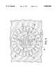
- FIG. 1depicts an elevational cross-sectional view of an electrostatic chuck embodying the present invention
- FIG. 2depicts a horizontal cross-sectional view of the chuck taken generally along the line 2--2 in FIG. 1 in the direction of the arrows;
- FIG. 3depicts an electrical schematic showing the connections of the DC voltage, RF power supply and heating current supply to the electrostatic chuck electrodes
- FIG. 4depicts a partial view of alternative electrode structure, namely, a mesh or lattice electrode
- FIG. 5depicts an elevational cross-sectional view of an electrostatic chuck of a horizontal cross-sectional view of the chuck in FIG. 2 containing cutout portions in the electrodes;
- FIG. 6depicts a horizontal cross-sectional view of an alternative electrode arrangement having half-moon shaped electrodes
- FIG. 7depicts a horizontal cross-sectional view of an alternative electrode arrangement having a single electrode.
- the chuck 10includes a body 12 of ceramic material having a pair of electrodes 14 and 16 embedded therein.
- the electrode 16is an inner circular electrode
- the electrode 14is an outer annular electrode concentric with and spaced apart from the inner electrode 16.
- the two electrodes 14 and 16are generally horizontally coplanar.
- Two electrical connectors or feedthroughs 18 and 19are formed integrally with the outer annular electrode 14 and two electrical connectors or feedthroughs 21 and 22 are formed integrally with the inner circular electrode 16.
- the body 12 of ceramic material and the electrodes 14 and 16 and feedthroughs 18, 19, 21 and 22have substantially the same coefficient of expansion.
- the body 12 of ceramic materialmay be aluminum-nitride having a coefficient of expansion of about 4.4 ⁇ 10 -6 /K°
- the electrodes 14 and 16 and the feedthroughs 18, 19, 21 and 22may be, for example, molybdenum having a coefficient of expansion of about 5.2 ⁇ 10 -6 /K°.
- Each electrode 14 and 16is generally a solid plate having a thickness of between 10 and 500 ⁇ m.
- molybdenumhas a resistance of 5.4 ⁇ -cm and the resistivity changes very little with temperature, i.e., 0.47%/K°.
- Other materialssuch as titanium or tungsten would also operate well as electrode material.
- the feedthrough connectorsare also fabricated of molybdenum, titanium or tungsten and have a diameter of about 0.1 to 0.5 inches (0.25 to 1.25 cm).
- FIG. 3depicts a schematic of the electronics used to drive the electrodes 14 and 16 of the embodiment of the invention in FIG. 2.
- the outer annular electrode 14is indicated diagrammatically by the element 14 and the inner circular electrode 16 is indicated diagrammatically by the element 16.
- the feedthroughs 18 and 19 for the electrode 14are indicated diagrammatically by the circles 18 and 19, and the feedthroughs 21 and 22 for the electrode 16 are represented by the circles 21 and 22.
- a suitable source of DC voltage 24is connected by lead 25 to feedthrough 21 and thereby to the electrode 16, and is connected by lines 26, 27 and 29 to the feedthrough 18 and thereby to the electrode 14.
- the application of the DC voltage 24 to the feedthroughs 21 and 18applies the DC voltage to the respective electrodes 16 and 14 to establish an electric field for electrostatically attracting and chucking a semiconductor wafer 50 to the top or support surface 30 (FIG. 1) of the electrostatic chuck 10.
- RF power from a suitable RF power supply 32is connected through capacitor 33, lead 34 to the feedthrough 21 and thereby to the electrode 16. In this manner, the RF power supply 32 applies RF biasing power to the inner circular electrode 16. Additionally, RF power from the RF power supply 32 is connected through capacitor 36, lead 37, lead 27 and lead 29 to the feedthrough 18 and thereby to the outer annular electrode 14 to apply RF biasing power to the outer annular electrode 14.
- the capacitors 33 and 36are provided to prevent shorting the DC voltage supply 24.
- the RF power supply 36could be connected to the electrodes 14 and 16 through feedthroughs 19 and 22 and through suitable capacitors and leads.
- the resistor R1represents the resistance of the electrode 16 and the resistor R2 represents the resistance of the electrode 14.
- a suitable heating current supply 40is provided and is connected to the feedthroughs 21 and 22 of the inner circular electrode 16 by leads 42 and 43. The supply 40 applies heating current to the inner circular electrode 16 to heat the electrode and thereby heat a semiconductor wafer 50 residing on the top 30, FIG. 1, of the electrostatic chuck 10.
- a suitable heating current supply 44is provided and is connected to the feedthroughs 18 and 19 of the outer annular electrode 14 by leads 45 and 46.
- the supply 44applies heating current to the electrode 14 (resistor R2) to heat the electrode and thereby heat the semiconductor wafer 50 chucked electrostatically to the top surface 30 (FIG. 1) of the electrostatic chuck 10. It will be understood that, depending upon heating current levels required, only one of the AC heating current supplies may be used and that when both supplies are used dual zone heating is possible, i.e., heating different portions of the wafer differing amounts.
- the present inventionalso includes the electrostatic chuck of FIGS. 1 and 2 in combination with the electrical components depicted schematically in FIG. 3, namely, the DC voltage supply 24, RF power supply 32, one or both of the heating current supplies 40 and 44, capacitors 33 and 36 and the associated leads providing the interconnections described above.
- FIG. 4depicts an alternative to the solid circular electrode 16 and outer annular electrode 14 shown in FIGS. 1 and 2.
- the alternative electrodesmay be suitable metal lattice or mesh electrodes such as the mesh or lattice electrode 150 shown in FIG. 4.
- a mesh electrodemore evenly distributes the DC voltage from the DC supply 24, the RF power from the RF supply 32 and heating current from one or more of the heating current supplies 40 and 44. As such, using a mesh electrode may result in more uniform wafer processing.
- FIG. 5depicts a top plan, cutaway view of an alternative arrangement of a pair of electrodes 200 and 202.
- These electrodes 200 and 202have a similar plan form as electrodes 14 and 16 of FIG. 2 in that electrode 200 is an inner circular electrode, and electrode 202 is an outer annular electrode concentric with and spaced apart from the inner electrode 200.
- Each electrode 200 and 202contains a plurality "cut out" portions 204, where each cut out portion extends partially across the electrode. The cut out portions alternate by extending alternately from each side edge of the electrode.
- the current path from one feedthrough 206, 210 to another respective feedthrough 208, 212is serpentine (as shown by the dotted lines 214 and 216).
- Such an extensive current pathincreases the heating capability of each electrode.
- the current pathscan be shortened or lengthened relative to one another to provide tailored heat generation, i.e., to facilitate zonal heating.
- This bipolar electrode structureis driven using the same electronics as depicted in FIG. 3.
- FIG. 6depicts another alternative embodiment of the electrode structure of the present invention.
- the pair of electrodesis arranged as two half-moon shaped electrodes 300 and 302.
- the electrodes 300 and 302can be formed with cut out portions 304, as shown or solid electrodes (not shown). With cut out portions, the current from each respective feedthrough 306, 310 to its other respective feedthrough 308, 312 flows in a serpentine path 314, 316 through each electrode 300, 302.
- This bipolar electrode structureis driven using the same electronics as depicted in FIG. 3.
- FIG. 7depicts another alternative embodiment of the electrode structure of the present invention.
- a single electrode 400 for a monopolar electrostatic chuckis depicted in a cutaway top plan view.
- a monopolar chuckuses a single electrode 400 that is biased with DC and RF voltages relative to a grounded wafer. The wafer is grounded either through use of a contact electrode providing a path from the wafer to ground or through use of a conductive plasma providing a path from the wafer to the grounded chamber walls.
- the single electrode 400has a pair of feedthrough connectors 402 and 406 located proximate the edges of the electrode 400. The feedthroughs are spaced sufficiently apart to provide a conductive path there between to produce heat.
- cut out portions 404may be used to provide a serpentine current path 408 for the heating current.
- the RF bias poweris coupled to one feedthrough 402 or 406
- the heating current supplyis connected to both feedthroughs 402 and 406
- the chucking voltage supplyis coupled to one or both feedthroughs 402 or 406.
- Electrodes 14 and 16 of FIGS. 1 and 2electrostatic chucking of a semiconductor wafer is accomplished, RF biasing of the chuck and wafer is accomplished, and heating of the chuck and wafer is accomplished.
- additional electrodescould be used to provide zonal chucking and zonal heating.
Landscapes
- Engineering & Computer Science (AREA)
- Physics & Mathematics (AREA)
- Condensed Matter Physics & Semiconductors (AREA)
- General Physics & Mathematics (AREA)
- Manufacturing & Machinery (AREA)
- Computer Hardware Design (AREA)
- Microelectronics & Electronic Packaging (AREA)
- Power Engineering (AREA)
- Container, Conveyance, Adherence, Positioning, Of Wafer (AREA)
Abstract
Description
1. Field of the Invention
This invention relates generally to an electrostatic chuck and, more particularly, this invention relates to an electrostatic chuck containing electrodes that are used for chucking a substrate, biasing a substrate and heating a substrate.
2. Description of the Background Art
Electrostatic chucks are known for electrostatically attracting and retaining a substrate such as a semiconductor wafer during wafer processing such as, for example, by physical vapor deposition (PVD), chemical vapor deposition (CVD) and etching. An example of the structure and function of an electrostatic chuck is set forth in U.S. Pat. No. 5,117,121, entitled METHOD OF AND APPARATUS FOR APPLYING A VOLTAGE TO ELECTROSTATIC CHUCK, patented May 26, 1992, Watanabe et al. inventors; this patent is incorporated herein by reference. As taught in this incorporated patent, a pair of electrodes is embedded in a sheet of relatively low resistivity ceramic material, and DC voltage is applied to the electrodes to create an electric field. When a semiconductor wafer is placed on the chuck, the electric field causes charges to accumulate on the backside of the wafer and opposite charges migrate to the surface of the chuck that is supporting the wafer. The oppositely charged surfaces electrostatically attract the semiconductor wafer to the chuck according to the Johnsen-Rahbek effect. Other known electrostatic chucks embed a pair of electrodes in a body of dielectric material to electrostatically attract a semiconductor wafer utilizing a Coulombic effect, i.e., the charges on the backside of the wafer and those on the electrodes attract one another.
In PVD chambers, the electrostatic chuck is typically mounted to a pedestal that is centrally located in the chamber. To RF bias the wafer, RF power is coupled directly to the pedestal, i.e., the pedestal forms a cathode electrode, and the RF power is coupled indirectly through the electrostatic chuck to the semiconductor wafer. As such, RF power losses are experienced due to the indirect coupling of the RF power through the chuck to the semiconductor wafer.
In certain semiconductor wafer processing applications, such as the PVD deposition of titanium on a semiconductor wafer, the semiconductor wafer is advantageously heated to enhance the adhesion of the deposited titanium to the wafer. Typically, a resistive heater is used to supply heat to the wafer. The heater is generally a resistive coil embedded in the ceramic material of the electrostatic chuck, or the heater may be embedded in a plate of stainless steel that is attached to the bottom of the electrostatic chuck. In either case, the heat produced by the heater must couple through the chuck material and the chuck electrode material before reaching the wafer. Such heating from the bottom of the chuck can produce a substantial thermal gradient vertically across the chuck. Furthermore, non-uniform thermal coupling through chuck can produce non-uniform heating of the wafer that results in non-uniform deposition characteristics.
Accordingly, there is a need in the art for an electrostatic chuck with fewer component parts than prior electrostatic chucks and which provides for DC voltage biasing for electrostatic chucking, RF power biasing and semiconductor wafer heating using a single electrode structure.
The disadvantages associated with the prior art are overcome by an electrostatic chuck including a body of ceramic material, a pair of electrodes embedded in the body of ceramic material, and two feedthroughs connected to each of the electrodes for receiving DC chucking voltage, RF biasing power, and electric heating current. As such, the invention uses a single pair of electrodes for biasing, chucking and heating a wafer. Consequently, a semiconductor wafer processing system incorporating the invention will have a simplified pedestal assembly and a wafer supported by the inventive chuck will experience more uniform processing.
The teachings of the present invention can be readily understood by considering the following detailed description in conjunction with the accompanying drawings, in which:
FIG. 1 depicts an elevational cross-sectional view of an electrostatic chuck embodying the present invention;
FIG. 2 depicts a horizontal cross-sectional view of the chuck taken generally along theline 2--2 in FIG. 1 in the direction of the arrows;
FIG. 3 depicts an electrical schematic showing the connections of the DC voltage, RF power supply and heating current supply to the electrostatic chuck electrodes;
FIG. 4 depicts a partial view of alternative electrode structure, namely, a mesh or lattice electrode;
FIG. 5 depicts an elevational cross-sectional view of an electrostatic chuck of a horizontal cross-sectional view of the chuck in FIG. 2 containing cutout portions in the electrodes;
FIG. 6 depicts a horizontal cross-sectional view of an alternative electrode arrangement having half-moon shaped electrodes; and
FIG. 7 depicts a horizontal cross-sectional view of an alternative electrode arrangement having a single electrode.
To facilitate understanding, identical reference numerals have been used, where possible, to designate identical elements that are common to the figures.
Referring now to FIGS. 1 and 2, there is shown anelectrostatic chuck 10 embodying the present invention. Thechuck 10 includes abody 12 of ceramic material having a pair ofelectrodes electrode 16 is an inner circular electrode, and theelectrode 14 is an outer annular electrode concentric with and spaced apart from theinner electrode 16. The twoelectrodes feedthroughs annular electrode 14 and two electrical connectors orfeedthroughs circular electrode 16. Thebody 12 of ceramic material and theelectrodes feedthroughs body 12 of ceramic material may be aluminum-nitride having a coefficient of expansion of about 4.4×10⁻⁶ /K°, and theelectrodes feedthroughs electrode
FIG. 3 depicts a schematic of the electronics used to drive theelectrodes annular electrode 14 is indicated diagrammatically by theelement 14 and the innercircular electrode 16 is indicated diagrammatically by theelement 16. Thefeedthroughs electrode 14 are indicated diagrammatically by thecircles feedthroughs electrode 16 are represented by thecircles
A suitable source ofDC voltage 24 is connected bylead 25 tofeedthrough 21 and thereby to theelectrode 16, and is connected bylines feedthrough 18 and thereby to theelectrode 14. The application of theDC voltage 24 to thefeedthroughs respective electrodes semiconductor wafer 50 to the top or support surface 30 (FIG. 1) of theelectrostatic chuck 10.
RF power from a suitableRF power supply 32 is connected throughcapacitor 33, lead 34 to thefeedthrough 21 and thereby to theelectrode 16. In this manner, theRF power supply 32 applies RF biasing power to the innercircular electrode 16. Additionally, RF power from theRF power supply 32 is connected throughcapacitor 36,lead 37,lead 27 andlead 29 to thefeedthrough 18 and thereby to the outerannular electrode 14 to apply RF biasing power to the outerannular electrode 14. Thecapacitors DC voltage supply 24. Alternatively, theRF power supply 36 could be connected to theelectrodes feedthroughs
With regard to the application of heating current to thechuck 10 in FIG. 3, the resistor R1 represents the resistance of theelectrode 16 and the resistor R2 represents the resistance of theelectrode 14. A suitable heatingcurrent supply 40, generally an AC supply, is provided and is connected to thefeedthroughs circular electrode 16 byleads supply 40 applies heating current to the innercircular electrode 16 to heat the electrode and thereby heat asemiconductor wafer 50 residing on thetop 30, FIG. 1, of theelectrostatic chuck 10. Similarly, a suitable heatingcurrent supply 44, generally an AC supply, is provided and is connected to thefeedthroughs annular electrode 14 byleads supply 44 applies heating current to the electrode 14 (resistor R2) to heat the electrode and thereby heat the semiconductor wafer 50 chucked electrostatically to the top surface 30 (FIG. 1) of theelectrostatic chuck 10. It will be understood that, depending upon heating current levels required, only one of the AC heating current supplies may be used and that when both supplies are used dual zone heating is possible, i.e., heating different portions of the wafer differing amounts.
It will be understood that the present invention also includes the electrostatic chuck of FIGS. 1 and 2 in combination with the electrical components depicted schematically in FIG. 3, namely, theDC voltage supply 24,RF power supply 32, one or both of the heating current supplies 40 and 44,capacitors
FIG. 4 depicts an alternative to the solidcircular electrode 16 and outerannular electrode 14 shown in FIGS. 1 and 2. The alternative electrodes may be suitable metal lattice or mesh electrodes such as the mesh orlattice electrode 150 shown in FIG. 4. A mesh electrode more evenly distributes the DC voltage from theDC supply 24, the RF power from theRF supply 32 and heating current from one or more of the heating current supplies 40 and 44. As such, using a mesh electrode may result in more uniform wafer processing.
FIG. 5 depicts a top plan, cutaway view of an alternative arrangement of a pair ofelectrodes 200 and 202. Theseelectrodes 200 and 202 have a similar plan form aselectrodes electrode 200 is an inner circular electrode, and electrode 202 is an outer annular electrode concentric with and spaced apart from theinner electrode 200. Eachelectrode 200 and 202 contains a plurality "cut out"portions 204, where each cut out portion extends partially across the electrode. The cut out portions alternate by extending alternately from each side edge of the electrode. As such, the current path from onefeedthrough respective feedthrough lines 214 and 216). Such an extensive current path increases the heating capability of each electrode. The current paths can be shortened or lengthened relative to one another to provide tailored heat generation, i.e., to facilitate zonal heating. This bipolar electrode structure is driven using the same electronics as depicted in FIG. 3.
FIG. 6 depicts another alternative embodiment of the electrode structure of the present invention. In this embodiment, the pair of electrodes is arranged as two half-moon shapedelectrodes electrodes portions 304, as shown or solid electrodes (not shown). With cut out portions, the current from eachrespective feedthrough respective feedthrough serpentine path electrode
FIG. 7 depicts another alternative embodiment of the electrode structure of the present invention. In this embodiment, asingle electrode 400 for a monopolar electrostatic chuck is depicted in a cutaway top plan view. A monopolar chuck uses asingle electrode 400 that is biased with DC and RF voltages relative to a grounded wafer. The wafer is grounded either through use of a contact electrode providing a path from the wafer to ground or through use of a conductive plasma providing a path from the wafer to the grounded chamber walls. Thesingle electrode 400 has a pair offeedthrough connectors electrode 400. The feedthroughs are spaced sufficiently apart to provide a conductive path there between to produce heat. As with the other electrodes, cut out portions 404 (shown in phantom) may be used to provide a serpentinecurrent path 408 for the heating current. In this embodiment, the RF bias power is coupled to onefeedthrough feedthroughs feedthroughs
In brief summary, it will be understood that with the use of as few as two electrodes, (for example,electrodes
It will be understood by those skilled in the art that many variations and modifications may be made in the present invention without departing from the spirit and the scope thereof.
Claims (24)
1. An electrostatic chuck comprising:
a body of dielectric material;
at least one electrode embedded in said body of dielectric material; and
two feedthroughs connected to said at least one electrode for receiving DC voltage for electrostatic chucking, for receiving RF power for RF biasing of the chuck, and for receiving heating current for heating said electrostatic chuck.
2. The electrostatic chuck according to claim 1 wherein said at least one electrode comprises a pair of electrodes.
3. The electrostatic chuck according to claim 2 wherein said pair of electrodes comprises an inner circular electrode and an outer annular electrode concentric with and spaced from the inner electrode.
4. The electrostatic chuck according to claim 1 wherein the at least one electrode is a mesh electrode.
5. The electrostatic chuck according to claim 1 wherein said body of dielectric material and said at least one electrode and said feedthroughs have substantially the same coefficient of expansion.
6. The electrostatic chuck according to claim 5 wherein said body of dielectric material is aluminum-nitride and wherein said at least one electrode and said feedthroughs are molybdenum.
7. The electrostatic chuck according to claim 1 wherein said at least one electrode comprises a pair of electrodes, each electrode having two feedthroughs, said two feedthroughs connected to each electrode of said pair of electrodes includes a first pair of feedthroughs connected to one electrode of said pair of electrodes and a second pair of feedthroughs connected to the other electrode of said pair of electrodes, one feedthrough of each pair of feedthroughs for receiving the DC voltage for electrostatic chucking, one feedthrough of each pair of feedthroughs connected through a capacitor for receiving the RF power for RF biasing of the chuck, and at least one pair of said feedthroughs for receiving the heating current for heating said electrostatic chuck.
8. The electrostatic chuck according to claim 7 wherein each pair of said feedthroughs is for receiving AC heating current to provide dual heating of said electrostatic chuck.
9. The electrostatic chuck of claim 1 wherein said at least one electrode contains at least one cut out portion.
10. The electrostatic chuck of claim 9 wherein at least one cut out portion is a plurality of portions, where each portion alternately extends from an opposing side edge of said at least one electrode.
11. The electrostatic chuck of claim 1 wherein said at least one electrode is a pair of electrodes that are half-moon shaped, where each of the electrodes is connected to two feedthroughs.
12. The electrostatic chuck of claim 11 wherein said electrodes contain at least one cut out portion.
13. The electrostatic chuck of claim 11 wherein at least one cut out portion is a plurality of portions, where each portion alternatively extends from an opposing side edge of said electrode.
14. Combination electrostatic chuck apparatus, comprising:
an electrostatic chuck including a body of ceramic material, first and second electrodes embedded in said body of ceramic material, a first pair of feedthroughs connected to said first electrode and a second pair of feedthroughs connected to said second electrode;
a DC voltage supply connected to said first electrode through one feedthrough of said first pair of feedthroughs and to said second electrode through one feedthrough of said second pair of feedthroughs for electrostatic chucking of a semiconductor wafer to said body of ceramic material;
a RF power supply connected to said first electrode through a first capacitor and through one feedthrough of said first pair of feedthroughs and to said second electrode through a second capacitor and through one feedthrough of said second pair of feedthroughs to couple RF power to said first electrode and said second electrode for RF biasing of said electrostatic chuck; and
at least one heating current supply connected to said first pair of feedthroughs to connect RF heating current to said first electrode to heat said chuck.
15. The apparatus according to claim 14 wherein said apparatus includes a second heating current supply connected to said second pair of feedthroughs to connect heating current to the second electrode to provide dual zone heating of said electrostatic chuck.
16. The apparatus according to claim 14 wherein said first and second electrodes comprise an inner circular electrode and an outer annular electrode concentric with and spaced from the inner electrode.
17. The apparatus of claim 14 wherein the first and second electrodes is a mesh electrode.
18. The apparatus of claim 14 wherein said body of ceramic material and said first and second electrodes and said feedthroughs have substantially the same coefficient of expansion.
19. The apparatus of claim 14 wherein said body of ceramic material is aluminum-nitride and wherein said first and second electrodes and said feedthroughs are molybdenum.
20. The apparatus of claim 14 wherein said first and second electrodes contains at least one cut out portion.
21. The apparatus of claim 20 wherein at least one cut out portion is a plurality of portions, where each portion alternately extends from an opposing side edge of said first and second electrodes.
22. The apparatus of claim 14 wherein said first and second electrodes are half-moon shaped.
23. The apparatus of claim 22 wherein said half-moon shaped electrodes contain at least one cut out portion.
24. The apparatus of claim 23 wherein at least one cut out portion is a plurality of portions, where each portion alternatively extends from an opposing side edge of said electrodes.
Priority Applications (1)
| Application Number | Priority Date | Filing Date | Title |
|---|---|---|---|
| US09/111,104US5886866A (en) | 1998-07-06 | 1998-07-06 | Electrostatic chuck having a combination electrode structure for substrate chucking, heating and biasing |
Applications Claiming Priority (1)
| Application Number | Priority Date | Filing Date | Title |
|---|---|---|---|
| US09/111,104US5886866A (en) | 1998-07-06 | 1998-07-06 | Electrostatic chuck having a combination electrode structure for substrate chucking, heating and biasing |
Publications (1)
| Publication Number | Publication Date |
|---|---|
| US5886866Atrue US5886866A (en) | 1999-03-23 |
Family
ID=22336629
Family Applications (1)
| Application Number | Title | Priority Date | Filing Date |
|---|---|---|---|
| US09/111,104Expired - LifetimeUS5886866A (en) | 1998-07-06 | 1998-07-06 | Electrostatic chuck having a combination electrode structure for substrate chucking, heating and biasing |
Country Status (1)
| Country | Link |
|---|---|
| US (1) | US5886866A (en) |
Cited By (49)
| Publication number | Priority date | Publication date | Assignee | Title |
|---|---|---|---|---|
| WO2000075970A1 (en)* | 1999-06-09 | 2000-12-14 | Applied Materials, Inc. | Substrate support for plasma processing |
| US6291777B1 (en)* | 1999-02-17 | 2001-09-18 | Applied Materials, Inc. | Conductive feed-through for creating a surface electrode connection within a dielectric body and method of fabricating same |
| US6367413B1 (en) | 1999-06-15 | 2002-04-09 | Tokyo Electron Limited | Apparatus for monitoring substrate biasing during plasma processing of a substrate |
| US6395095B1 (en) | 1999-06-15 | 2002-05-28 | Tokyo Electron Limited | Process apparatus and method for improved plasma processing of a substrate |
| US6431112B1 (en) | 1999-06-15 | 2002-08-13 | Tokyo Electron Limited | Apparatus and method for plasma processing of a substrate utilizing an electrostatic chuck |
| US6492612B1 (en)* | 1998-12-28 | 2002-12-10 | Tokyo Electron Limited | Plasma apparatus and lower electrode thereof |
| US6577113B2 (en) | 2001-06-06 | 2003-06-10 | Tokyo Electron Limited | Apparatus and method for measuring substrate biasing during plasma processing of a substrate |
| US20040233608A1 (en)* | 2003-05-21 | 2004-11-25 | Tokyo Electron Limited Of Tbs Broadcast Center | Apparatus and methods for compensating plasma sheath non-uniformities at the substrate in a plasma processing system |
| US20040233264A1 (en)* | 2003-05-24 | 2004-11-25 | Smith David E. | Media electrostatic hold down and conductive heating assembly |
| US20050190250A1 (en)* | 2004-02-26 | 2005-09-01 | Hewlett-Packard Development Company, L.P. | Media hold down system |
| US20060158821A1 (en)* | 2003-06-17 | 2006-07-20 | Kinya Miyashita | Dipolar electrostatic chuck |
| US20060234604A1 (en)* | 2000-08-30 | 2006-10-19 | Micron Technology, Inc. | Methods and apparatus for electrical, mechanical and/or chemical removal of conductive material from a microelectronic substrate |
| US20070000441A1 (en)* | 2005-07-01 | 2007-01-04 | Applied Materials, Inc. | Scalable uniform thermal plate |
| US20070081295A1 (en)* | 2005-10-11 | 2007-04-12 | Applied Materials, Inc. | Capacitively coupled plasma reactor having a cooled/heated wafer support with uniform temperature distribution |
| US20070081296A1 (en)* | 2005-10-11 | 2007-04-12 | Applied Materials, Inc. | Method of operating a capacitively coupled plasma reactor with dual temperature control loops |
| US20070081294A1 (en)* | 2005-10-11 | 2007-04-12 | Applied Materials, Inc. | Capacitively coupled plasma reactor having very agile wafer temperature control |
| US20070091538A1 (en)* | 2005-10-20 | 2007-04-26 | Buchberger Douglas A Jr | Plasma reactor with wafer backside thermal loop, two-phase internal pedestal thermal loop and a control processor governing both loops |
| US20070097580A1 (en)* | 2005-10-11 | 2007-05-03 | Applied Materials, Inc. | Method of cooling a wafer support at a uniform temperature in a capacitively coupled plasma reactor |
| US20070165356A1 (en)* | 2003-04-22 | 2007-07-19 | Applied Materials, Inc. | Substrate support having heat transfer system |
| US20070209933A1 (en)* | 2006-03-09 | 2007-09-13 | Ken Yoshioka | Sample holding electrode and a plasma processing apparatus using the same |
| US20090089971A1 (en)* | 2007-09-25 | 2009-04-09 | Vanderlinden Roger P | Sealed pick-up head for a mobile sweeper |
| US20090288943A1 (en)* | 2008-05-21 | 2009-11-26 | Byung Sung Kwak | Thin film batteries and methods for manufacturing same |
| US20100101771A1 (en)* | 2008-10-24 | 2010-04-29 | Applied Materials, Inc. | Heated cooling plate for e-chucks and pedestals |
| US20110024047A1 (en)* | 2003-04-22 | 2011-02-03 | Applied Materials, Inc. | Substrate support having fluid channel |
| US20110092072A1 (en)* | 2009-10-21 | 2011-04-21 | Lam Research Corporation | Heating plate with planar heating zones for semiconductor processing |
| US20110143462A1 (en)* | 2009-12-15 | 2011-06-16 | Lam Research Corporation | Adjusting substrate temperature to improve cd uniformity |
| JP2012089694A (en)* | 2010-10-20 | 2012-05-10 | Sumitomo Electric Ind Ltd | Wafer holder of 2 layer rf structure |
| WO2013039718A1 (en)* | 2011-09-16 | 2013-03-21 | Lam Research Corporation | A component of a substrate support assembly producing localized magnetic fields |
| CN103066000A (en)* | 2011-10-19 | 2013-04-24 | 中芯国际集成电路制造(上海)有限公司 | Wafer bearing device and method of wafer bearing |
| CN103065997A (en)* | 2011-10-19 | 2013-04-24 | 中芯国际集成电路制造(上海)有限公司 | Wafer bearing device and method of wafer bearing |
| US8461674B2 (en) | 2011-09-21 | 2013-06-11 | Lam Research Corporation | Thermal plate with planar thermal zones for semiconductor processing |
| US8546732B2 (en) | 2010-11-10 | 2013-10-01 | Lam Research Corporation | Heating plate with planar heater zones for semiconductor processing |
| US8624168B2 (en) | 2011-09-20 | 2014-01-07 | Lam Research Corporation | Heating plate with diode planar heater zones for semiconductor processing |
| JP2014027159A (en)* | 2012-07-27 | 2014-02-06 | Panasonic Corp | Plasma processing apparatus and plasma processing method |
| US8809747B2 (en) | 2012-04-13 | 2014-08-19 | Lam Research Corporation | Current peak spreading schemes for multiplexed heated array |
| US8861170B2 (en) | 2009-05-15 | 2014-10-14 | Entegris, Inc. | Electrostatic chuck with photo-patternable soft protrusion contact surface |
| US8879233B2 (en) | 2009-05-15 | 2014-11-04 | Entegris, Inc. | Electrostatic chuck with polymer protrusions |
| US9025305B2 (en) | 2010-05-28 | 2015-05-05 | Entegris, Inc. | High surface resistivity electrostatic chuck |
| US20150221540A1 (en)* | 2014-02-05 | 2015-08-06 | Micron Technology, Inc. | Devices, systems and methods for electrostatic force enhanced semiconductor bonding |
| US9307578B2 (en) | 2011-08-17 | 2016-04-05 | Lam Research Corporation | System and method for monitoring temperatures of and controlling multiplexed heater array |
| US9324589B2 (en) | 2012-02-28 | 2016-04-26 | Lam Research Corporation | Multiplexed heater array using AC drive for semiconductor processing |
| US9543187B2 (en) | 2008-05-19 | 2017-01-10 | Entegris, Inc. | Electrostatic chuck |
| US20170211185A1 (en)* | 2016-01-22 | 2017-07-27 | Applied Materials, Inc. | Ceramic showerhead with embedded conductive layers |
| US10236201B2 (en) | 2013-12-06 | 2019-03-19 | Applied Materials, Inc. | Wafer carrier for smaller wafers and wafer pieces |
| US10568163B2 (en) | 2010-10-22 | 2020-02-18 | Lam Research Corporation | Methods of fault detection for multiplexed heater array |
| CN111937132A (en)* | 2018-04-04 | 2020-11-13 | 朗姆研究公司 | Electrostatic chuck with sealing surface |
| US20220130704A1 (en)* | 2020-10-23 | 2022-04-28 | Applied Materials, Inc. | Bipolar electrostatic chuck to limit dc discharge |
| US11450511B2 (en) | 2020-11-16 | 2022-09-20 | Applied Materials, Inc. | Methods and apparatus for zone control of RF bias for stress uniformity |
| US20250125180A1 (en)* | 2023-10-11 | 2025-04-17 | Applied Materials, Inc. | Bipolar electrostatic chuck electrode with self-induced dc voltage |
Citations (15)
| Publication number | Priority date | Publication date | Assignee | Title |
|---|---|---|---|---|
| US4502094A (en)* | 1981-09-14 | 1985-02-26 | U.S. Philips Corporation | Electrostatic chuck |
| US5166856A (en)* | 1991-01-31 | 1992-11-24 | International Business Machines Corporation | Electrostatic chuck with diamond coating |
| US5191506A (en)* | 1991-05-02 | 1993-03-02 | International Business Machines Corporation | Ceramic electrostatic chuck |
| US5280156A (en)* | 1990-12-25 | 1994-01-18 | Ngk Insulators, Ltd. | Wafer heating apparatus and with ceramic substrate and dielectric layer having electrostatic chucking means |
| US5567267A (en)* | 1992-11-20 | 1996-10-22 | Tokyo Electron Limited | Method of controlling temperature of susceptor |
| US5581874A (en)* | 1994-03-28 | 1996-12-10 | Tokyo Electron Limited | Method of forming a bonding portion |
| US5584971A (en)* | 1993-07-02 | 1996-12-17 | Tokyo Electron Limited | Treatment apparatus control method |
| US5606484A (en)* | 1993-06-23 | 1997-02-25 | Shin-Etsu Chemical Co., Ltd. | Ceramic electrostatic chuck with built-in heater |
| US5663865A (en)* | 1995-02-20 | 1997-09-02 | Shin-Etsu Chemical Co., Ltd. | Ceramic electrostatic chuck with built-in heater |
| US5665260A (en)* | 1993-12-27 | 1997-09-09 | Shin-Etsu Chemical Co., Ltd. | Ceramic electrostatic chuck with built-in heater |
| US5671116A (en)* | 1995-03-10 | 1997-09-23 | Lam Research Corporation | Multilayered electrostatic chuck and method of manufacture thereof |
| US5708556A (en)* | 1995-07-10 | 1998-01-13 | Watkins Johnson Company | Electrostatic chuck assembly |
| US5708250A (en)* | 1996-03-29 | 1998-01-13 | Lam Resarch Corporation | Voltage controller for electrostatic chuck of vacuum plasma processors |
| US5737178A (en)* | 1997-03-06 | 1998-04-07 | Applied Materials, Inc. | Monocrystalline ceramic coating having integral bonding interconnects for electrostatic chucks |
| US5737175A (en)* | 1996-06-19 | 1998-04-07 | Lam Research Corporation | Bias-tracking D.C. power circuit for an electrostatic chuck |
- 1998
- 1998-07-06USUS09/111,104patent/US5886866A/ennot_activeExpired - Lifetime
Patent Citations (15)
| Publication number | Priority date | Publication date | Assignee | Title |
|---|---|---|---|---|
| US4502094A (en)* | 1981-09-14 | 1985-02-26 | U.S. Philips Corporation | Electrostatic chuck |
| US5280156A (en)* | 1990-12-25 | 1994-01-18 | Ngk Insulators, Ltd. | Wafer heating apparatus and with ceramic substrate and dielectric layer having electrostatic chucking means |
| US5166856A (en)* | 1991-01-31 | 1992-11-24 | International Business Machines Corporation | Electrostatic chuck with diamond coating |
| US5191506A (en)* | 1991-05-02 | 1993-03-02 | International Business Machines Corporation | Ceramic electrostatic chuck |
| US5567267A (en)* | 1992-11-20 | 1996-10-22 | Tokyo Electron Limited | Method of controlling temperature of susceptor |
| US5606484A (en)* | 1993-06-23 | 1997-02-25 | Shin-Etsu Chemical Co., Ltd. | Ceramic electrostatic chuck with built-in heater |
| US5584971A (en)* | 1993-07-02 | 1996-12-17 | Tokyo Electron Limited | Treatment apparatus control method |
| US5665260A (en)* | 1993-12-27 | 1997-09-09 | Shin-Etsu Chemical Co., Ltd. | Ceramic electrostatic chuck with built-in heater |
| US5581874A (en)* | 1994-03-28 | 1996-12-10 | Tokyo Electron Limited | Method of forming a bonding portion |
| US5663865A (en)* | 1995-02-20 | 1997-09-02 | Shin-Etsu Chemical Co., Ltd. | Ceramic electrostatic chuck with built-in heater |
| US5671116A (en)* | 1995-03-10 | 1997-09-23 | Lam Research Corporation | Multilayered electrostatic chuck and method of manufacture thereof |
| US5708556A (en)* | 1995-07-10 | 1998-01-13 | Watkins Johnson Company | Electrostatic chuck assembly |
| US5708250A (en)* | 1996-03-29 | 1998-01-13 | Lam Resarch Corporation | Voltage controller for electrostatic chuck of vacuum plasma processors |
| US5737175A (en)* | 1996-06-19 | 1998-04-07 | Lam Research Corporation | Bias-tracking D.C. power circuit for an electrostatic chuck |
| US5737178A (en)* | 1997-03-06 | 1998-04-07 | Applied Materials, Inc. | Monocrystalline ceramic coating having integral bonding interconnects for electrostatic chucks |
Cited By (113)
| Publication number | Priority date | Publication date | Assignee | Title |
|---|---|---|---|---|
| US6492612B1 (en)* | 1998-12-28 | 2002-12-10 | Tokyo Electron Limited | Plasma apparatus and lower electrode thereof |
| US6291777B1 (en)* | 1999-02-17 | 2001-09-18 | Applied Materials, Inc. | Conductive feed-through for creating a surface electrode connection within a dielectric body and method of fabricating same |
| US6273958B2 (en) | 1999-06-09 | 2001-08-14 | Applied Materials, Inc. | Substrate support for plasma processing |
| WO2000075970A1 (en)* | 1999-06-09 | 2000-12-14 | Applied Materials, Inc. | Substrate support for plasma processing |
| US6596550B2 (en) | 1999-06-15 | 2003-07-22 | Tokyo Electron Limited | Method for monitoring substrate biasing during plasma processing of a substrate |
| US6367413B1 (en) | 1999-06-15 | 2002-04-09 | Tokyo Electron Limited | Apparatus for monitoring substrate biasing during plasma processing of a substrate |
| US6395095B1 (en) | 1999-06-15 | 2002-05-28 | Tokyo Electron Limited | Process apparatus and method for improved plasma processing of a substrate |
| US6431112B1 (en) | 1999-06-15 | 2002-08-13 | Tokyo Electron Limited | Apparatus and method for plasma processing of a substrate utilizing an electrostatic chuck |
| US20060234604A1 (en)* | 2000-08-30 | 2006-10-19 | Micron Technology, Inc. | Methods and apparatus for electrical, mechanical and/or chemical removal of conductive material from a microelectronic substrate |
| US6577113B2 (en) | 2001-06-06 | 2003-06-10 | Tokyo Electron Limited | Apparatus and method for measuring substrate biasing during plasma processing of a substrate |
| US20070165356A1 (en)* | 2003-04-22 | 2007-07-19 | Applied Materials, Inc. | Substrate support having heat transfer system |
| US8279577B2 (en) | 2003-04-22 | 2012-10-02 | Applied Materials, Inc. | Substrate support having fluid channel |
| US7768765B2 (en) | 2003-04-22 | 2010-08-03 | Applied Materials, Inc. | Substrate support having heat transfer system |
| US20110024047A1 (en)* | 2003-04-22 | 2011-02-03 | Applied Materials, Inc. | Substrate support having fluid channel |
| US20040233608A1 (en)* | 2003-05-21 | 2004-11-25 | Tokyo Electron Limited Of Tbs Broadcast Center | Apparatus and methods for compensating plasma sheath non-uniformities at the substrate in a plasma processing system |
| US7075771B2 (en) | 2003-05-21 | 2006-07-11 | Tokyo Electron Limited | Apparatus and methods for compensating plasma sheath non-uniformities at the substrate in a plasma processing system |
| US20040233264A1 (en)* | 2003-05-24 | 2004-11-25 | Smith David E. | Media electrostatic hold down and conductive heating assembly |
| US7216968B2 (en)* | 2003-05-24 | 2007-05-15 | Hewlett-Packard Development Company, L.P. | Media electrostatic hold down and conductive heating assembly |
| US7567421B2 (en)* | 2003-06-17 | 2009-07-28 | Creative Technology Corporation | Bipolar electrostatic chuck |
| US20060158821A1 (en)* | 2003-06-17 | 2006-07-20 | Kinya Miyashita | Dipolar electrostatic chuck |
| US6997549B2 (en)* | 2004-02-26 | 2006-02-14 | Hewlett-Packard Development Company, L.P. | Media hold down system |
| US20050190250A1 (en)* | 2004-02-26 | 2005-09-01 | Hewlett-Packard Development Company, L.P. | Media hold down system |
| US20070000441A1 (en)* | 2005-07-01 | 2007-01-04 | Applied Materials, Inc. | Scalable uniform thermal plate |
| US8337660B2 (en) | 2005-10-11 | 2012-12-25 | B/E Aerospace, Inc. | Capacitively coupled plasma reactor having very agile wafer temperature control |
| US8157951B2 (en) | 2005-10-11 | 2012-04-17 | Applied Materials, Inc. | Capacitively coupled plasma reactor having very agile wafer temperature control |
| US8092638B2 (en) | 2005-10-11 | 2012-01-10 | Applied Materials Inc. | Capacitively coupled plasma reactor having a cooled/heated wafer support with uniform temperature distribution |
| US20070097580A1 (en)* | 2005-10-11 | 2007-05-03 | Applied Materials, Inc. | Method of cooling a wafer support at a uniform temperature in a capacitively coupled plasma reactor |
| US8801893B2 (en) | 2005-10-11 | 2014-08-12 | Be Aerospace, Inc. | Method of cooling a wafer support at a uniform temperature in a capacitively coupled plasma reactor |
| US20070081294A1 (en)* | 2005-10-11 | 2007-04-12 | Applied Materials, Inc. | Capacitively coupled plasma reactor having very agile wafer temperature control |
| US8034180B2 (en) | 2005-10-11 | 2011-10-11 | Applied Materials, Inc. | Method of cooling a wafer support at a uniform temperature in a capacitively coupled plasma reactor |
| US7988872B2 (en) | 2005-10-11 | 2011-08-02 | Applied Materials, Inc. | Method of operating a capacitively coupled plasma reactor with dual temperature control loops |
| US20070081296A1 (en)* | 2005-10-11 | 2007-04-12 | Applied Materials, Inc. | Method of operating a capacitively coupled plasma reactor with dual temperature control loops |
| US20070081295A1 (en)* | 2005-10-11 | 2007-04-12 | Applied Materials, Inc. | Capacitively coupled plasma reactor having a cooled/heated wafer support with uniform temperature distribution |
| US20100300621A1 (en)* | 2005-10-11 | 2010-12-02 | Paul Lukas Brillhart | Method of cooling a wafer support at a uniform temperature in a capacitively coupled plasma reactor |
| US20100303680A1 (en)* | 2005-10-11 | 2010-12-02 | Buchberger Douglas A Jr | Capacitively coupled plasma reactor having very agile wafer temperature control |
| US20100314046A1 (en)* | 2005-10-20 | 2010-12-16 | Paul Lukas Brillhart | Plasma reactor with a multiple zone thermal control feed forward control apparatus |
| US20070091540A1 (en)* | 2005-10-20 | 2007-04-26 | Applied Materials, Inc. | Method of processing a workpiece in a plasma reactor using multiple zone feed forward thermal control |
| US8546267B2 (en) | 2005-10-20 | 2013-10-01 | B/E Aerospace, Inc. | Method of processing a workpiece in a plasma reactor using multiple zone feed forward thermal control |
| US20100319851A1 (en)* | 2005-10-20 | 2010-12-23 | Buchberger Jr Douglas A | Plasma reactor with feed forward thermal control system using a thermal model for accommodating rf power changes or wafer temperature changes |
| US8608900B2 (en) | 2005-10-20 | 2013-12-17 | B/E Aerospace, Inc. | Plasma reactor with feed forward thermal control system using a thermal model for accommodating RF power changes or wafer temperature changes |
| US20110065279A1 (en)* | 2005-10-20 | 2011-03-17 | Buchberger Jr Douglas A | Method of processing a workpiece in a plasma reactor using feed forward thermal control |
| US20110068085A1 (en)* | 2005-10-20 | 2011-03-24 | Paul Lukas Brillhart | Method of processing a workpiece in a plasma reactor using multiple zone feed forward thermal control |
| US8980044B2 (en) | 2005-10-20 | 2015-03-17 | Be Aerospace, Inc. | Plasma reactor with a multiple zone thermal control feed forward control apparatus |
| US20070091538A1 (en)* | 2005-10-20 | 2007-04-26 | Buchberger Douglas A Jr | Plasma reactor with wafer backside thermal loop, two-phase internal pedestal thermal loop and a control processor governing both loops |
| US20070089834A1 (en)* | 2005-10-20 | 2007-04-26 | Applied Materials, Inc. | Plasma reactor with a multiple zone thermal control feed forward control apparatus |
| US8012304B2 (en) | 2005-10-20 | 2011-09-06 | Applied Materials, Inc. | Plasma reactor with a multiple zone thermal control feed forward control apparatus |
| US8021521B2 (en) | 2005-10-20 | 2011-09-20 | Applied Materials, Inc. | Method for agile workpiece temperature control in a plasma reactor using a thermal model |
| US20070091539A1 (en)* | 2005-10-20 | 2007-04-26 | Applied Materials, Inc. | Plasma reactor with feed forward thermal control system using a thermal model for accommodating RF power changes or wafer temperature changes |
| US8092639B2 (en) | 2005-10-20 | 2012-01-10 | Advanced Thermal Sciences Corporation | Plasma reactor with feed forward thermal control system using a thermal model for accommodating RF power changes or wafer temperature changes |
| US20070091537A1 (en)* | 2005-10-20 | 2007-04-26 | Applied Materials, Inc. | Method for agile workpiece temperature control in a plasma reactor using a thermal model |
| US8329586B2 (en) | 2005-10-20 | 2012-12-11 | Applied Materials, Inc. | Method of processing a workpiece in a plasma reactor using feed forward thermal control |
| US20070091541A1 (en)* | 2005-10-20 | 2007-04-26 | Applied Materials, Inc. | Method of processing a workpiece in a plasma reactor using feed forward thermal control |
| US8221580B2 (en) | 2005-10-20 | 2012-07-17 | Applied Materials, Inc. | Plasma reactor with wafer backside thermal loop, two-phase internal pedestal thermal loop and a control processor governing both loops |
| US20070209933A1 (en)* | 2006-03-09 | 2007-09-13 | Ken Yoshioka | Sample holding electrode and a plasma processing apparatus using the same |
| US20090089971A1 (en)* | 2007-09-25 | 2009-04-09 | Vanderlinden Roger P | Sealed pick-up head for a mobile sweeper |
| US10395963B2 (en) | 2008-05-19 | 2019-08-27 | Entegris, Inc. | Electrostatic chuck |
| US9543187B2 (en) | 2008-05-19 | 2017-01-10 | Entegris, Inc. | Electrostatic chuck |
| US20090288943A1 (en)* | 2008-05-21 | 2009-11-26 | Byung Sung Kwak | Thin film batteries and methods for manufacturing same |
| US8568571B2 (en) | 2008-05-21 | 2013-10-29 | Applied Materials, Inc. | Thin film batteries and methods for manufacturing same |
| US20100101771A1 (en)* | 2008-10-24 | 2010-04-29 | Applied Materials, Inc. | Heated cooling plate for e-chucks and pedestals |
| US9064911B2 (en) | 2008-10-24 | 2015-06-23 | Applied Materials, Inc. | Heated cooling plate for E-chucks and pedestals |
| US8879233B2 (en) | 2009-05-15 | 2014-11-04 | Entegris, Inc. | Electrostatic chuck with polymer protrusions |
| US9721821B2 (en) | 2009-05-15 | 2017-08-01 | Entegris, Inc. | Electrostatic chuck with photo-patternable soft protrusion contact surface |
| US8861170B2 (en) | 2009-05-15 | 2014-10-14 | Entegris, Inc. | Electrostatic chuck with photo-patternable soft protrusion contact surface |
| US10720346B2 (en) | 2009-10-21 | 2020-07-21 | Lam Research Corporation | Substrate support with thermal zones for semiconductor processing |
| US10236193B2 (en) | 2009-10-21 | 2019-03-19 | Lam Research Corporation | Substrate supports with multi-layer structure including independent operated heater zones |
| US9646861B2 (en) | 2009-10-21 | 2017-05-09 | Lam Research Corporation | Heating plate with heating zones for substrate processing and method of use thereof |
| US8637794B2 (en) | 2009-10-21 | 2014-01-28 | Lam Research Corporation | Heating plate with planar heating zones for semiconductor processing |
| US20110092072A1 (en)* | 2009-10-21 | 2011-04-21 | Lam Research Corporation | Heating plate with planar heating zones for semiconductor processing |
| US8884194B2 (en) | 2009-10-21 | 2014-11-11 | Lam Research Corporation | Heating plate with planar heater zones for semiconductor processing |
| US9392643B2 (en) | 2009-10-21 | 2016-07-12 | Lam Research Corporation | Heating plate with planar heater zones for semiconductor processing |
| US8642480B2 (en) | 2009-12-15 | 2014-02-04 | Lam Research Corporation | Adjusting substrate temperature to improve CD uniformity |
| US10056225B2 (en) | 2009-12-15 | 2018-08-21 | Lam Research Corporation | Adjusting substrate temperature to improve CD uniformity |
| US20110143462A1 (en)* | 2009-12-15 | 2011-06-16 | Lam Research Corporation | Adjusting substrate temperature to improve cd uniformity |
| US9025305B2 (en) | 2010-05-28 | 2015-05-05 | Entegris, Inc. | High surface resistivity electrostatic chuck |
| JP2012089694A (en)* | 2010-10-20 | 2012-05-10 | Sumitomo Electric Ind Ltd | Wafer holder of 2 layer rf structure |
| US10568163B2 (en) | 2010-10-22 | 2020-02-18 | Lam Research Corporation | Methods of fault detection for multiplexed heater array |
| US8680441B2 (en) | 2010-11-10 | 2014-03-25 | Lam Research Corporation | Heating plate with planar heater zones for semiconductor processing |
| US8546732B2 (en) | 2010-11-10 | 2013-10-01 | Lam Research Corporation | Heating plate with planar heater zones for semiconductor processing |
| US9307578B2 (en) | 2011-08-17 | 2016-04-05 | Lam Research Corporation | System and method for monitoring temperatures of and controlling multiplexed heater array |
| US9713200B2 (en) | 2011-08-17 | 2017-07-18 | Lam Research Corporation | System and method for monitoring temperatures of and controlling multiplexed heater array |
| US10872748B2 (en) | 2011-09-16 | 2020-12-22 | Lam Research Corporation | Systems and methods for correcting non-uniformities in plasma processing of substrates |
| WO2013039718A1 (en)* | 2011-09-16 | 2013-03-21 | Lam Research Corporation | A component of a substrate support assembly producing localized magnetic fields |
| US10388493B2 (en) | 2011-09-16 | 2019-08-20 | Lam Research Corporation | Component of a substrate support assembly producing localized magnetic fields |
| US8624168B2 (en) | 2011-09-20 | 2014-01-07 | Lam Research Corporation | Heating plate with diode planar heater zones for semiconductor processing |
| US8461674B2 (en) | 2011-09-21 | 2013-06-11 | Lam Research Corporation | Thermal plate with planar thermal zones for semiconductor processing |
| US8587113B2 (en) | 2011-09-21 | 2013-11-19 | Lam Research Corporation | Thermal plate with planar thermal zones for semiconductor processing |
| US20130100572A1 (en)* | 2011-10-19 | 2013-04-25 | Semiconductor Manufacturing International Corp. | Apparatus and method for holding a wafer |
| CN103065997A (en)* | 2011-10-19 | 2013-04-24 | 中芯国际集成电路制造(上海)有限公司 | Wafer bearing device and method of wafer bearing |
| CN103066000B (en)* | 2011-10-19 | 2015-11-25 | 中芯国际集成电路制造(上海)有限公司 | The method of wafer carrying equipment and wafer carrying |
| CN103066000A (en)* | 2011-10-19 | 2013-04-24 | 中芯国际集成电路制造(上海)有限公司 | Wafer bearing device and method of wafer bearing |
| CN103065997B (en)* | 2011-10-19 | 2015-08-05 | 中芯国际集成电路制造(上海)有限公司 | The method of wafer carrying equipment and wafer carrying |
| US8917489B2 (en)* | 2011-10-19 | 2014-12-23 | Semiconductor Manufacturing International Corp. | Apparatus and method for holding a wafer |
| US9775194B2 (en) | 2012-02-28 | 2017-09-26 | Lam Research Corporation | Multiplexed heater array using AC drive for semiconductor processing |
| US9324589B2 (en) | 2012-02-28 | 2016-04-26 | Lam Research Corporation | Multiplexed heater array using AC drive for semiconductor processing |
| US8809747B2 (en) | 2012-04-13 | 2014-08-19 | Lam Research Corporation | Current peak spreading schemes for multiplexed heated array |
| JP2014027159A (en)* | 2012-07-27 | 2014-02-06 | Panasonic Corp | Plasma processing apparatus and plasma processing method |
| US10236201B2 (en) | 2013-12-06 | 2019-03-19 | Applied Materials, Inc. | Wafer carrier for smaller wafers and wafer pieces |
| US10153190B2 (en)* | 2014-02-05 | 2018-12-11 | Micron Technology, Inc. | Devices, systems and methods for electrostatic force enhanced semiconductor bonding |
| US12040211B2 (en) | 2014-02-05 | 2024-07-16 | Micron Technology, Inc. | Devices, systems and methods for electrostatic force enhanced semiconductor bonding |
| CN106062938A (en)* | 2014-02-05 | 2016-10-26 | 美光科技公司 | Devices, systems and methods for electrostatic force enhanced semiconductor bonding |
| US11574834B2 (en) | 2014-02-05 | 2023-02-07 | Micron Technology, Inc. | Devices, systems and methods for electrostatic force enhanced semiconductor bonding |
| US20150221540A1 (en)* | 2014-02-05 | 2015-08-06 | Micron Technology, Inc. | Devices, systems and methods for electrostatic force enhanced semiconductor bonding |
| US11114328B2 (en) | 2014-02-05 | 2021-09-07 | Micron Technology, Inc. | Devices, systems and methods for electrostatic force enhanced semiconductor bonding |
| US20170211185A1 (en)* | 2016-01-22 | 2017-07-27 | Applied Materials, Inc. | Ceramic showerhead with embedded conductive layers |
| US20210013080A1 (en)* | 2018-04-04 | 2021-01-14 | Lam Research Corporation | Electrostatic chuck with seal surface |
| CN111937132A (en)* | 2018-04-04 | 2020-11-13 | 朗姆研究公司 | Electrostatic chuck with sealing surface |
| US12142509B2 (en)* | 2018-04-04 | 2024-11-12 | Lam Research Corporation | Electrostatic chuck with seal surface |
| US20220130704A1 (en)* | 2020-10-23 | 2022-04-28 | Applied Materials, Inc. | Bipolar electrostatic chuck to limit dc discharge |
| US12057339B2 (en)* | 2020-10-23 | 2024-08-06 | Applied Materials, Inc. | Bipolar electrostatic chuck to limit DC discharge |
| TWI867253B (en)* | 2020-10-23 | 2024-12-21 | 美商應用材料股份有限公司 | Substrate support assembly with bipolar electrostatic chuck to limit dc discharge |
| US11450511B2 (en) | 2020-11-16 | 2022-09-20 | Applied Materials, Inc. | Methods and apparatus for zone control of RF bias for stress uniformity |
| US20250125180A1 (en)* | 2023-10-11 | 2025-04-17 | Applied Materials, Inc. | Bipolar electrostatic chuck electrode with self-induced dc voltage |
Similar Documents
| Publication | Publication Date | Title |
|---|---|---|
| US5886866A (en) | Electrostatic chuck having a combination electrode structure for substrate chucking, heating and biasing | |
| US6215643B1 (en) | Electrostatic chuck and production method therefor | |
| US20230340668A1 (en) | Wafer holder | |
| KR100916953B1 (en) | Ceramic Electrostatic Chuck Assembly And Method Of Manufacturing The Same | |
| US6081414A (en) | Apparatus for improved biasing and retaining of a workpiece in a workpiece processing system | |
| KR100626118B1 (en) | Cathode assembly including an electrostatic chuck for holding a wafer in a semiconductor wafer processing system | |
| KR100702876B1 (en) | Apparatus providing high frequency return current path control in semiconductor wafer processing systems | |
| US6259592B1 (en) | Apparatus for retaining a workpiece upon a workpiece support and method of manufacturing same | |
| US5671116A (en) | Multilayered electrostatic chuck and method of manufacture thereof | |
| US6104596A (en) | Apparatus for retaining a subtrate in a semiconductor wafer processing system and a method of fabricating same | |
| US6088213A (en) | Bipolar electrostatic chuck and method of making same | |
| EP0049588A2 (en) | Method and apparatus for dry etching and electrostatic chucking device used therein | |
| US6067222A (en) | Substrate support apparatus and method for fabricating same | |
| US5909355A (en) | Ceramic electrostatic chuck and method of fabricating same | |
| CN110226222B (en) | Electrostatic chuck with radio frequency isolation heater | |
| US6535372B2 (en) | Controlled resistivity boron nitride electrostatic chuck apparatus for retaining a semiconductor wafer and method of fabricating the same | |
| JPWO2007043519A1 (en) | Wafer heating apparatus having electrostatic adsorption function | |
| JP3287996B2 (en) | Electrostatic chuck device | |
| US12108498B2 (en) | Wafer placement table | |
| JP4367685B2 (en) | Electrostatic chuck device | |
| US20250176075A1 (en) | Ceramic heater | |
| KR20110064665A (en) | Bipolar Electrostatic Chuck Using Electric Field Gradient | |
| JPH1131736A (en) | Electrostatic suction stage for semiconductor manufacturing equipment | |
| CN120303777A (en) | Electrostatic chuck heater and film forming device |
Legal Events
| Date | Code | Title | Description |
|---|---|---|---|
| AS | Assignment | Owner name:APPLIED MATERIALS, INC., CALIFORNIA Free format text:ASSIGNMENT OF ASSIGNORS INTEREST;ASSIGNOR:HAUSMANN, GILBERT;REEL/FRAME:009304/0682 Effective date:19980706 | |
| STCF | Information on status: patent grant | Free format text:PATENTED CASE | |
| FPAY | Fee payment | Year of fee payment:4 | |
| FPAY | Fee payment | Year of fee payment:8 | |
| FPAY | Fee payment | Year of fee payment:12 |