US5885855A - Method for distributing connection pads on a semiconductor die - Google Patents
Method for distributing connection pads on a semiconductor dieDownload PDFInfo
- Publication number
- US5885855A US5885855AUS08/909,312US90931297AUS5885855AUS 5885855 AUS5885855 AUS 5885855AUS 90931297 AUS90931297 AUS 90931297AUS 5885855 AUS5885855 AUS 5885855A
- Authority
- US
- United States
- Prior art keywords
- power
- bump
- sector
- bump pads
- die
- Prior art date
- Legal status (The legal status is an assumption and is not a legal conclusion. Google has not performed a legal analysis and makes no representation as to the accuracy of the status listed.)
- Expired - Lifetime
Links
Images


Classifications
- H—ELECTRICITY
- H01—ELECTRIC ELEMENTS
- H01L—SEMICONDUCTOR DEVICES NOT COVERED BY CLASS H10
- H01L24/00—Arrangements for connecting or disconnecting semiconductor or solid-state bodies; Methods or apparatus related thereto
- H01L24/01—Means for bonding being attached to, or being formed on, the surface to be connected, e.g. chip-to-package, die-attach, "first-level" interconnects; Manufacturing methods related thereto
- H01L24/02—Bonding areas ; Manufacturing methods related thereto
- H01L24/04—Structure, shape, material or disposition of the bonding areas prior to the connecting process
- H01L24/05—Structure, shape, material or disposition of the bonding areas prior to the connecting process of an individual bonding area
- H—ELECTRICITY
- H01—ELECTRIC ELEMENTS
- H01L—SEMICONDUCTOR DEVICES NOT COVERED BY CLASS H10
- H01L23/00—Details of semiconductor or other solid state devices
- H01L23/48—Arrangements for conducting electric current to or from the solid state body in operation, e.g. leads, terminal arrangements ; Selection of materials therefor
- H01L23/50—Arrangements for conducting electric current to or from the solid state body in operation, e.g. leads, terminal arrangements ; Selection of materials therefor for integrated circuit devices, e.g. power bus, number of leads
- H—ELECTRICITY
- H01—ELECTRIC ELEMENTS
- H01L—SEMICONDUCTOR DEVICES NOT COVERED BY CLASS H10
- H01L2224/00—Indexing scheme for arrangements for connecting or disconnecting semiconductor or solid-state bodies and methods related thereto as covered by H01L24/00
- H01L2224/01—Means for bonding being attached to, or being formed on, the surface to be connected, e.g. chip-to-package, die-attach, "first-level" interconnects; Manufacturing methods related thereto
- H01L2224/02—Bonding areas; Manufacturing methods related thereto
- H01L2224/04—Structure, shape, material or disposition of the bonding areas prior to the connecting process
- H01L2224/05—Structure, shape, material or disposition of the bonding areas prior to the connecting process of an individual bonding area
- H01L2224/0554—External layer
- H01L2224/05599—Material
- H—ELECTRICITY
- H01—ELECTRIC ELEMENTS
- H01L—SEMICONDUCTOR DEVICES NOT COVERED BY CLASS H10
- H01L2924/00—Indexing scheme for arrangements or methods for connecting or disconnecting semiconductor or solid-state bodies as covered by H01L24/00
- H01L2924/0001—Technical content checked by a classifier
- H01L2924/00014—Technical content checked by a classifier the subject-matter covered by the group, the symbol of which is combined with the symbol of this group, being disclosed without further technical details
- H—ELECTRICITY
- H01—ELECTRIC ELEMENTS
- H01L—SEMICONDUCTOR DEVICES NOT COVERED BY CLASS H10
- H01L2924/00—Indexing scheme for arrangements or methods for connecting or disconnecting semiconductor or solid-state bodies as covered by H01L24/00
- H01L2924/01—Chemical elements
- H01L2924/01005—Boron [B]
- H—ELECTRICITY
- H01—ELECTRIC ELEMENTS
- H01L—SEMICONDUCTOR DEVICES NOT COVERED BY CLASS H10
- H01L2924/00—Indexing scheme for arrangements or methods for connecting or disconnecting semiconductor or solid-state bodies as covered by H01L24/00
- H01L2924/01—Chemical elements
- H01L2924/01006—Carbon [C]
- H—ELECTRICITY
- H01—ELECTRIC ELEMENTS
- H01L—SEMICONDUCTOR DEVICES NOT COVERED BY CLASS H10
- H01L2924/00—Indexing scheme for arrangements or methods for connecting or disconnecting semiconductor or solid-state bodies as covered by H01L24/00
- H01L2924/01—Chemical elements
- H01L2924/01014—Silicon [Si]
- H—ELECTRICITY
- H01—ELECTRIC ELEMENTS
- H01L—SEMICONDUCTOR DEVICES NOT COVERED BY CLASS H10
- H01L2924/00—Indexing scheme for arrangements or methods for connecting or disconnecting semiconductor or solid-state bodies as covered by H01L24/00
- H01L2924/01—Chemical elements
- H01L2924/01033—Arsenic [As]
- H—ELECTRICITY
- H01—ELECTRIC ELEMENTS
- H01L—SEMICONDUCTOR DEVICES NOT COVERED BY CLASS H10
- H01L2924/00—Indexing scheme for arrangements or methods for connecting or disconnecting semiconductor or solid-state bodies as covered by H01L24/00
- H01L2924/01—Chemical elements
- H01L2924/01082—Lead [Pb]
- H—ELECTRICITY
- H01—ELECTRIC ELEMENTS
- H01L—SEMICONDUCTOR DEVICES NOT COVERED BY CLASS H10
- H01L2924/00—Indexing scheme for arrangements or methods for connecting or disconnecting semiconductor or solid-state bodies as covered by H01L24/00
- H01L2924/013—Alloys
- H01L2924/014—Solder alloys
- H—ELECTRICITY
- H01—ELECTRIC ELEMENTS
- H01L—SEMICONDUCTOR DEVICES NOT COVERED BY CLASS H10
- H01L2924/00—Indexing scheme for arrangements or methods for connecting or disconnecting semiconductor or solid-state bodies as covered by H01L24/00
- H01L2924/10—Details of semiconductor or other solid state devices to be connected
- H01L2924/11—Device type
- H01L2924/14—Integrated circuits
- H—ELECTRICITY
- H01—ELECTRIC ELEMENTS
- H01L—SEMICONDUCTOR DEVICES NOT COVERED BY CLASS H10
- H01L2924/00—Indexing scheme for arrangements or methods for connecting or disconnecting semiconductor or solid-state bodies as covered by H01L24/00
- H01L2924/15—Details of package parts other than the semiconductor or other solid state devices to be connected
- H01L2924/151—Die mounting substrate
- H01L2924/1517—Multilayer substrate
- H01L2924/15172—Fan-out arrangement of the internal vias
- H01L2924/15173—Fan-out arrangement of the internal vias in a single layer of the multilayer substrate
- H—ELECTRICITY
- H01—ELECTRIC ELEMENTS
- H01L—SEMICONDUCTOR DEVICES NOT COVERED BY CLASS H10
- H01L2924/00—Indexing scheme for arrangements or methods for connecting or disconnecting semiconductor or solid-state bodies as covered by H01L24/00
- H01L2924/30—Technical effects
- H01L2924/301—Electrical effects
- H01L2924/30107—Inductance
Definitions
- This inventionrelates to integrated circuit packaging, and more particularly to an efficiently designed integrated circuit flip-chip die providing access to chip signals.
- Modern high performance integrated circuit, or IC, chipsrequire large numbers of interconnections between the upper level IC structure, or die, and the lower level IC structure, or package.
- the large number of interconnectionsare necessary to perform complex operations.
- Prior methods for providing these interconnectionsinclude wire bonding, wherein the die is mounted to the package or substrate with connections between the top surface of the die and the surface of the package. The die and package are then mounted to the motherboard.
- Another known method for providing connectionsis through tape automated bonding (TAB).
- TABtape automated bonding
- These methodsare inherently inefficient for providing power and I/O to the die because limited space is available on the periphery of the die for wire bond or tape pads. Space at the periphery of the die which must be used for bonding translates into space which is unavailable for active circuitry. Further, the resistance and limited inductance associated with the wiring connecting the surface of the die to the package is frequently inadequate for ICs having high performance requirements.
- a method used to join the die to the package which provides adequate bonding and power-I/O capabilityis the "flip-chip" packaging process.
- the flip-chip processutilizes an IC flip-chip, which is a monolithic semiconductor unit having bead-like solder bump terminals provided on one face of the chip. These bumps are densely packed together on the die surface, thereby facilitating electrical connections to the substrate.
- a flip-chip configurationprovides access to more core area for a given die size. Bump pitches of 250 micrometers on the surface of the flip-chip is typical. Allowing bumps over active circuitry yields greater silicon utilization.
- the proximity of the solder bumps on, the die to the associated terminals on the packagehave the further benefit of decreasing the overall resistance in transmitting power or signals between the package and the die, improving overall system performance.
- Pitch requirementstypically mandate regular intervals between the bumps, further limiting bump placement and organization.
- Current pitch requirements for typical package-die arrangementsare approximately 8 to 10 mils (center-to-center) between bumps for a flip-chip configuration.
- an arrangement of bump pads for use on a face of a semiconductor diecomprising four corner regions, each corner region comprising multiple I/O bump pads and power bump pads.
- the corner regionsadjoin two edges of said die, and layout of the corner region is a specialized arrangement depending upon the size of the die, signal to power ratios, and the core power requirements.
- the arrangementalso comprises multiple edge regions having multiple I/O bump pads and power bump pads. The edge regions are located along the edges of the die and are interleaved between the corner regions.
- corner regions and the edge regionsdepend upon the power to signal ratio of the region.
- a power to signal ratio of four to oneas shown in the preferred embodiment, four I/O signals per power signal pair (Vdd and Vss), exclusive of the core power required, is provided herein.
- Vdd and Vssfour I/O signals per power signal pair
- a corner region of six by six, or thirty six bumpsis provided arranged according to an method which designates the layout of the corner region to provide multiple sectors where power bump pads adjoin the edge of the die surface.
- a core power regionhaving multiple power bump pads. This power region is centrally located within the edge regions and the corner groups. As the core requirements may mandate an odd number of rows and columns of bumps for the core, an alternate embodiment provides a "checkerboard" arrangement wherein a balanced number of core power regions transmit power along power rails to the edge of the die surface.
- the preferred embodimenthas multiple power rails connecting the core power bumps to the edge of the surface of the die, where there is located a power ring.
- This power ringconnects the Vdd and Vss signals for all corner regions and edge regions, thereby providing power to the IC.
- the I/O bumpsare connected to I/O cells, and connections from I/O bumps to I/O cells requires that the I/O bump furthest from the I/O cell or power bumps be in one direction, such as to the right, while the second furthest I/O bump connect to its I/O cell in the opposite direction.
- first and fourth bumpsemanate redistribution traces in one direction, such as rightward, while second and fourth are in the opposite direction, such as leftward.
- Adjacent linear arrayshave redistribution traces emanating in opposite directions, such that the first I/O signal in one array emanates in a direction, such as rightward, while the first I/O signal in the adjacent arrays emanate in the opposite direction, say leftward.
- a die surface arrangementfor use where core power is not critical, or signal to power ratios are of little import.
- a die surface arrangementwith two power bumps, one live voltage, or power, bump and one ground bump, and multiple I/O bumps, all bumps linearly aligned, with the ground and power bumps both located intermediate between the I/O bumps.
- the ground, power, I/O bumpsform an array, and this array is replicated linearly across the die surface forming a linear array arrangement, where preferably redistribution traces for adjacent arrays emanate in opposite directions.
- the die surface arrangementcomprises multiple linear array arrangements interspersed with multiple linearly aligned core power bumps.
- FIG. 1is an illustration of the components used in mounting a semiconductor die
- FIG. 2illustrates implementation of an approximately five millimeter square flip-chip architecture having 400 bumps
- FIG. 3shows the arrangement of an individual bump pad column, including an array of bumps and connections for I/O signals and power
- FIG. 4Ais an illustration of a 36 bump corner region arrangement in accordance with the current invention.
- FIG. 4Bis an illustration of a 25 bump corner region arrangement in accordance with the current invention.
- FIG. 4Cis an illustration of a 49 bump corner region arrangement in accordance with the current invention.
- FIG. 4Dis an illustration of a 64 bump corner region arrangement in accordance with the current invention.
- FIG. 4E and 4Fare a flowchart demonstrating design of a corner region of dimension N+2 bumps by N+2 bumps, where N is the number of signals in an array;
- FIG. 5is an alternate embodiment of the power core wherein the core has an odd number of bumps
- FIG. 6is an alternate embodiment of an array for use with a die having decreased power or increased I/O requirements.
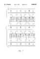
- FIG. 7is an implementation of a plurality of the arrays of FIG. 6 and associated power rails and bumps.
- FIG. 1illustrates a flip-chip semiconductor die 10 having a series of gates or other logic elements constructed on its downward-facing surface 11.
- the dieis mounted to a substrate 13 which is then affixed to a motherboard 14.
- Die 10is typically bonded to the substrate by solder bumps.
- FIG. 2presents the arrangement on the surface 11 of semiconductor die 10.
- Flip-chip die 10has dimensions of 5.0174 millimeters by 5.0524 millimeters, and located thereon is a set of 400 bumps or bump pads, comprising 20 rows of 20 bumps.
- Substrate 13is composed of any laminate material, such as ceramic or plastic wire traces through the layers leading from its top surface to underneath.
- the bumps on die 10are formed of a high quality metal.
- Power core bump pad block 201consists of 64 bumps which provide power to the core of the IC 12 and which transmit power to the peripheral power connections, or core power ring 202A, via a series of power rails 212-219.
- the power core bump pad block 201consists of a series of linearly aligned bump pads. The power bumps on the surface of the die supply power and ground to logic circuitry within the integrated circuit 12.
- the power core bump pad block 201 illustrated in this preferred embodimentconsists of four rows of Vss connections to the peripheral power ring 202 and four rows of Vdd connections connected to the peripheral power ring 202 via eight power rails 212-219.
- Peripheral power ring 202is divided into core power ring 202A and I/O power ring 202B.
- core power ring 202Ais divided into Vss core power ring 203A, Vdd core power ring 203B, Vdd I/O power ring 203C, and Vss I/O power ring 203D.
- the four rows of Vss bump padsalternate with the four rows of Vdd bump pads.
- the diealso comprises four edge regions 203, 205, 207, and 209, each edge region comprises a plurality of linearly aligned bump pad arrays, each linearly aligned bump pad array having four I/O bump pads, one Vdd bump pad, and one Vss bump pad, all linearly aligned.
- each edge regionattaches to the peripheral I/O power ring 202B and borders the power core bump pad block 201.
- the die 10also has four corner regions 204, 206, 208 and 210, each having an arrangement of 36 bump pads per corner region. Orientation of the thirty six bump pads in each corner region 204, 206, 208 and 210 provides adequate power to the cells as well as sufficient I/O connections to provide power to the cell and I/O capability. All I/O bumps are connected to one of the set of I/O cells 211 lining the periphery of the cell.
- the pattern illustrated in FIG. 1uses a single metal layer and provides power to the I/O cells 211 without dedicating individual slots for power use.
- the method for arranging the die as shown in FIG. 1requires first determining the ideal power/ground to signal ratio for the circuit. For every Vdd (power) and Vss (ground) power configuration, the die must comprise N I/O bumps based on the calculated ratio. For example, in the arrangement of FIG. 2, a four to one power/ground to signal ratio is possible, and for each Vdd and Vss power bump pad pair, N equals four because four I/O signals are provided, for a total of six bump pads. These six bump pads are arranged in columns and are replicated across the edge of the die 10 in edge regions 203, 205, 207 and 209.
- the corner regionsare special cases, and the same six-by-six corner regions are used for all embodiments having a four to one signal to power ratio (FIG. 4A).
- the total number of columns on the face of the die 10depends on the bump pitch, or distance between the bumps, where bump pitch is equal to N times the I/O device pitch, and N is an integer.
- I/O pitchis 63 micrometers
- the bump pad pitchis 252 micrometers (approximately 2.5 mils) for the four to one power ratio on the 5.0174 millimeter by 5.0524 millimeter die.
- Each array 300contains four I/O bump pads 301, 302, 303, and 304 and two power bump pads, a Vdd bump pad 305 and a Vss bump pad 306. These bump pads are arranged in a single column with the I/O bump pads 301, 302, 303, and 304 adjacent one another, the Vdd bump pad 305 neighboring the I/O bump pads, and the Vss bump pad 306 next to the Vdd bump pad 305.
- the Vss bump pad 306is thus closest to the periphery of the die 10 and the power ring 202.
- I/O bump pad redistribution traces 307, 308, 309, and 310couple the I/O bump pads 301, 302, 303 and 304 to the peripheral clusters of I/O cells 211.
- Vdd (power) bump 305is connected to Vdd bus 313 at power connection point 311, while Vss (ground) bump 306 intersects Vss bus 314 at ground connection point 312.
- This bump pad array 300is replicated through all the edge regions 203, 205, 207 and 209.
- the ratio of four I/O signals for each Vdd/Vss pairprovides adequate power/ground to signal ratio to supply the die, i.e. a ratio of four to one.
- the corner regionsare arranged as shown in FIGS. 4B-D, and the corner regions for other dimensions are generated using the process of FIGS. 4E-F.
- An alternate linear bump pad array arrangementreverses the locations of the signal bump pad 304 which is closest to the power bumps and the Vdd (power) bump 305.
- Such an arrangementthus comprises in order a series of three signal bump pads, the Vdd bump, the fourth signal bump pad, and the Vss bump.
- the I/O bump pad redistribution traces 307, 308, 309, and 310are wires which necessarily introduce resistance and inductance problems into the system.
- redistribution traces on adjacent linearly aligned bump pad arraysare arranged as mirror images of one another. For example, as shown in FIG. 3, first redistribution trace 307 is routed to the left of the bump pad array, second redistribution trace 308 to the right, third redistribution trace 309 to the left, and fourth redistribution trace 310 to the right.
- Adjacent linearly aligned bump pad arrayswould have a first redistribution trace routed to the right of the bump pad array, second redistribution trace to the left, and so on to balance overall resistance, inductance, and parasitics.
- FIG. 4Aillustrates the preferred embodiment of a corner region with a four to one signal to power ratio and where N equals four. This yields a six by six corner region arrangement.
- FIG. 4Billustrates a five by five corner region arrangement (N equal to three), while FIG. 4C is a seven by seven corner region, and FIG. 4D an eight by eight corner region.
- FIGS. 4E-FA flow chart for developing the corner region is presented in FIGS. 4E-F. As in these figures, corner regions must be square having dimensions (N+2) 2 .
- corner region 204An expanded view of corner region 204 is shown in FIG. 4A.
- Each corner regionconsists of 24 I/O bump pads, six Vdd bump pads, and six Vss bump pads, for a total of 36 bump pads.
- the same interconnections to the power ring 202 and the plurality of I/O cells 211are required and provided within the region.
- the corner region 204is divided into six distinct sectors: a corner region standard sector 41, a first left corner region sector 42, a first top corner region sector 43, a second left corner region sector 44, a second top corner region sector 45, and a corner region edge sector 46.
- the corner region standard sector 41 illustrated in FIG. 4Ahas a similar configuration to the linearly aligned bump pad array 300 illustrated in FIG. 3.
- the preferred embodiment of such an arrayis for the redistribution trace from the bump furthest from the edge of the die to radiate from the bump in the opposite direction as the next bump, as in FIG. 3.
- the first top corner region sector 42comprises four I/O bump pads, one Vss bump pad, and one Vdd bump pad, not linearly aligned.
- the bumpshave three signals, one Vdd and one Vss signal aligned in the column form suggested in FIG. 3, with an additional signal bump in the next leftmost remaining column.
- the first top corner region sector 43comprises a similar three signals in the topmost row, one Vdd and one Vss signal aligned in row form as in FIG. 3. Again, first top corner region array group 43 contains an additional I/O signal bump in the next row at the leftmost side.
- the second left corner region sector 44comprises one I/O bump pad, one Vss bump pad, and one Vdd bump pad, linearly aligned in the leftmost remaining row, and three I/O bumps in the next remaining leftmost row.
- Second top corner region sector 45has a single I/O bump pad, a single Vss bump pad, and a single Vdd bump pad linearly aligned, and the three remaining I/O cells also linearly aligned in the next topmost row.
- the remaining bump padsare allocated to the corner region edge sector 46. All signals feed into respective I/O cell clusters.
- the layout of the first left corner region sector 42is similar to and effectively the mirror image of first top corner region sector 43, and second left corner region sector 44 is similar to and effectively the mirror image of second top corner region sector 45. Placement of the Vdd and Vss bumps for all sectors is no further than two bumps from the peripheral edge of the die 10.
- the corner region 204 depicted in FIG. 4Ais used in all four corners of the die 10 and is available for any sized chip having 16 by 16 bumps or more on the surface 11 of the flip-chip die 10.
- the die surfacemust have a power core bump pad block 201 with dimensions of at least four by four, as smaller sized core bump dimensions do not provide both ground and power to the core.
- Standard row allocation step 401creates the first corner region row across the topmost row of the corner region. This row is similar to a standard row as in the edge regions 203, 205, 207, and 209 of FIG. 1.
- a counter Mis set to 1 in counter set step 402.
- leftmost remaining column establishment step 403within the leftmost remaining column, as many bump pads as may be located within the column are designated as the (M+1)th sector.
- topmost remaining row establishment step 404within the topmost remaining row, as many bump pads as may be located within the row are designated as the (M+2)th sector.
- steps 405 and 406are repeated by filling the leftmost remaining column and topmost remaining row with bump pads for the sector. This loop continues until the M+1 and M+2 sectors are complete.
- Multiple remaining sector evaluation step 409determines if more than one sector remains. If so, the process after the counter set step 402 is iteratively repeated until one or no sector remains. In last sector evaluation step 410, if only one N+2 sector remains, all bump pads in that sector are allocated as the final sector.
- connections to the cellsare allocated in a similar fashion to those shown in FIG. 4A.
- Connections between the bump pads and the I/O cells 204 and peripheral I/O power ring 202Brequire balanced I/O connections based on required resistance, conductance, and parasitic parameters.
- a balanced arrayrequires that the connection from the bump furthest from the power bumps in a linear array must emanate from the I/O bump in the opposite direction of the second furthest I/O bump as shown in the preferred embodiment of FIG. 3.
- This balancing in the topmost row of the corner regionrequires that the redistribution trace from the top left bump in the corner region 204 radiate upward while the redistribution trace from the second bump in the top row is downward.
- Vdd and Vss pads for each sectorare implemented no more than two bump pads away from the edge of the cell, as shown in FIGS. 4A-D, and in sector arrangements spanning greater than three columns or rows, Vdd and Vss bumps should be located whenever possible to a single side rather than in the center of the sector, as with the corner region edge sector 46 of FIG. 4A. As shown in sectors 6 and 7 of FIG. 4C, such an arrangement is not always possible, and so leftmost and topmost skewing of the Vdd and Vss power is necessary. I/O signals are routed to the respective peripheral I/O cells 211.
- the corner region allocation process of FIG. 4E-Fensures that Vdd and Vss bump pads are located at the outside edge of the cell, and neither power nor ground is more than two bump pads away from the edge of the cell. This procedure guarantees adequate power and I/O for each corner region.
- the same basic bump designapplies to larger bump pad matrices, and may apply to smaller sized arrays of at least 16 by 16 bumps with a four by four power core power bump pad block 11.
- the same 36 bump pad corner regions 204, 206, 208 and 210would occupy space on the die.
- the edge regions 203, 205, 207 and 209would be of increased dimension, i.e. for a 900 bump pad arrangement the edge regions would have 18 bump pad arrays each.
- the power core bump pad block 201 in such an arrangementwould increase to an 18 by 18 bump pad area, thereby providing increased power to the core.
- corner regions 204, 206, 208, and 210, edge regions 203, 205, 207, and 209 and power core bump pad block 201would also support a die 10 having rectangular dimensions.
- the corner regions 204, 206, 208, and 210remain square.
- Edge regions 203, 205, 207, and 209remain an array of columns having N+2 bump pads, but the number of columns would increase or decrease to accommodate the dimensions of the rectangular die.
- the power core bump pad block 201 in such an arrangementwould also have rectangular dimensions and the same plurality of power rails (although possibly increased in number) as shown in FIG. 2.
- FIG. 5A further arrangement the die surface is illustrated in FIG. 5.
- the bump pad arrangement of the power core bump pad block 201 when the die 10 consists of an odd number of power core bump padsrequires an alternate arrangement to overcome the inherent problem of having one additional row of power core bump pads, or one additional rail of either positive or ground which results.
- the second preferred embodimentis as illustrated in FIG. 5.
- the arrangement of FIG. 5is a seven by seven power core bump pad block, with eight rows of connections from live bumps to power ring 202 and eight rows of connections from ground bumps to power ring 202.
- This "checkerboard" arrangementprovides an equivalent number of ground and live voltage pads, with one additional bump pad per power core arrangement. As shown in FIG.
- the extra bump in the upper leftmay be null, power, or ground.
- the core bump pad arrangementalternates rows of voltage connections to the power ring 202, while each bump pad connects to the appropriate adjacent power rail. This "checkerboard" pattern results in equivalent balanced voltage and ground connections to the power ring 202 and does not use one of the 49 bump pads, supporting an odd number of bumps with an even number of power rails.
- Such an arrangementcan be advantageous when used in connection with bump depopulation, where for manufacturing positioning concerns, a bump is removed from a regular pattern.
- the odd bumpshould be located toward the center of the core array, but manufacturing positioning based on bump depopulation is ineffective if the missing bump is located in the exact center of the core array.
- the positioning of the I/O cells on the diemay be relocated from the periphery of the die and the core power cells may be moved from the center of the die.
- This third preferred embodimentprovides I/O bump pads at the expense of the power core bump pad block 11, and uses the power rails to transmit power to and from the I/O signal ring 211, thereby providing a mixed core-I/O voltage arrangement.
- This embodimentis used is used in situations where a single core and I/O power supply is employed.
- This embodimentprovides an alternative in a large bump arrangement on the surface of the die 10, where core power requirements are not as critical, or where signal/power ratios dictate an increased quantity of I/O bump pads can be supported or a decreased quantity of power bumps are necessary to support the die.
- Vdd bus 608 and Vss bus 609 and I/O cells 611are located in the middle of the bump pads, with I/O bumps 601 and 602 located above I/O cells 611 and I/O bumps 603 and 604 below the I/O cells 611.
- the Vdd voltage bump 605 and Vss ground bump 606are centrally located and aligned with the I/O bumps 601-604. Power and ground are supplied via Vdd bus 608 and Vss bus 609.
- FIG. 6illustrates an embodiment where N is 2, with two I/O cells and two power cells. I/O cells 611 are repeated along and across the die surface, providing the additional I/O for a fixed size region having less stringent power requirements. Power and I/O for this embodiment are routed to two edges of the die 10, and again a design supporting a rectangular die merely requires expanding the linear elements of FIG. 7 to accommodate die dimensions.
- the direction of the redistribution trace between the topmost I/O bump 601 and the corresponding I/O cell 609is preferably in the opposite direction of the second topmost I/O cell 602 and its corresponding I/O cell 610.
- the alternating trace arrangement for adjacent linearly aligned bumps outlined aboveshould be employed for the configuration shown in FIG. 6. That is, where the top redistribution trace from bump 601 is routed to the right of the linear bump array, the adjacent linear bump array preferably has its top redistribution trace routed to the left of the linear bump array.
- an odd number of I/O padswould be linearly aligned at one end of the power bumps, and an even number at the opposite end.
- the number of bumps above and below the power padsmust differ by one, but it is of no importance that the higher number be above or below, or the odd number above or below.
- the redistribution traces between the topmost I/O bump and the I/O cells in a linear array and the redistribution traces of adjacent arraysmust be opposite in direction to provide balanced resistance, inductance, and parasitics.
- the additional bumpsmay be designated as extra power bumps so that as the die grows and requires additional power, these extra bumps may be used instead of requiring a complete redesign. For example, if the signal to power requirement for the embodiment shown in FIGS. 2 and 3 was only three to one, the result would be a requirement for fewer I/O bumps. Aside from a rewiring of the edge regions and creating corner regions having dimension 5 by 5, the additional row of bumps around the outside of power core bump pad block 201 could be allocated as power bumps and used for future upgrades to the die.
Landscapes
- Engineering & Computer Science (AREA)
- Computer Hardware Design (AREA)
- Microelectronics & Electronic Packaging (AREA)
- Power Engineering (AREA)
- Physics & Mathematics (AREA)
- Condensed Matter Physics & Semiconductors (AREA)
- General Physics & Mathematics (AREA)
- Design And Manufacture Of Integrated Circuits (AREA)
- Semiconductor Integrated Circuits (AREA)
Abstract
Description
Claims (19)
Priority Applications (1)
| Application Number | Priority Date | Filing Date | Title |
|---|---|---|---|
| US08/909,312US5885855A (en) | 1996-11-12 | 1997-08-14 | Method for distributing connection pads on a semiconductor die |
Applications Claiming Priority (2)
| Application Number | Priority Date | Filing Date | Title |
|---|---|---|---|
| US08/747,325US5952726A (en) | 1996-11-12 | 1996-11-12 | Flip chip bump distribution on die |
| US08/909,312US5885855A (en) | 1996-11-12 | 1997-08-14 | Method for distributing connection pads on a semiconductor die |
Related Parent Applications (1)
| Application Number | Title | Priority Date | Filing Date |
|---|---|---|---|
| US08/747,325DivisionUS5952726A (en) | 1996-11-12 | 1996-11-12 | Flip chip bump distribution on die |
Publications (1)
| Publication Number | Publication Date |
|---|---|
| US5885855Atrue US5885855A (en) | 1999-03-23 |
Family
ID=25004608
Family Applications (2)
| Application Number | Title | Priority Date | Filing Date |
|---|---|---|---|
| US08/747,325Expired - LifetimeUS5952726A (en) | 1996-11-12 | 1996-11-12 | Flip chip bump distribution on die |
| US08/909,312Expired - LifetimeUS5885855A (en) | 1996-11-12 | 1997-08-14 | Method for distributing connection pads on a semiconductor die |
Family Applications Before (1)
| Application Number | Title | Priority Date | Filing Date |
|---|---|---|---|
| US08/747,325Expired - LifetimeUS5952726A (en) | 1996-11-12 | 1996-11-12 | Flip chip bump distribution on die |
Country Status (1)
| Country | Link |
|---|---|
| US (2) | US5952726A (en) |
Cited By (19)
| Publication number | Priority date | Publication date | Assignee | Title |
|---|---|---|---|---|
| US6207476B1 (en)* | 1999-06-10 | 2001-03-27 | Vlsi Technology, Inc. | Methods of packaging an integrated circuit and methods of forming an integrated circuit package |
| US6674166B2 (en)* | 1998-06-03 | 2004-01-06 | Lsi Logic Corporation | Flip-chip integrated circuit routing to I/O devices |
| US6689634B1 (en)* | 1999-09-22 | 2004-02-10 | Texas Instruments Incorporated | Modeling technique for selectively depopulating electrical contacts from a foot print of a grid array (BGA or LGA) package to increase device reliability |
| WO2004055890A1 (en)* | 2002-12-12 | 2004-07-01 | Sun Microsystems, Inc. | Method and apparatus for electrostatically aligning integrated circuits |
| US20050040539A1 (en)* | 2002-01-31 | 2005-02-24 | Carlsgaard Eric Stephen | Flip chip die bond pads, die bond pad placement and routing optimization |
| US20050127405A1 (en)* | 2003-12-11 | 2005-06-16 | Wang-Jin Chen | I/O circuit placement method and semiconductor device |
| US20070206062A1 (en)* | 2006-03-01 | 2007-09-06 | Lexmark International, Inc. | Flexible circuits, flexible circuit assemblies and assemblies for use with fluid ejection apparatuses |
| US20070245276A1 (en)* | 2002-07-12 | 2007-10-18 | Kabushiki Kaisha Toshiba | System, method and computer program product for designing connecting terminals of semiconductor device |
| US20090115072A1 (en)* | 2007-11-01 | 2009-05-07 | Texas Instruments Incorporated | BGA Package with Traces for Plating Pads Under the Chip |
| US20090283904A1 (en)* | 2008-05-15 | 2009-11-19 | Lsi Logic Corporation | Flipchip bump patterns for efficient i-mesh power distribution schemes |
| CN101473064B (en)* | 2006-06-16 | 2012-08-29 | 东丽工程株式会社 | Silicon thin-film and method of forming silicon thin-film |
| US20130207107A1 (en)* | 2012-02-10 | 2013-08-15 | Taiwan Semiconductor Manufacturing Company, Ltd. | Methods of of improving bump allocation for semiconductor devices and semiconductor devices with improved bump allocation |
| US9504156B1 (en)* | 2006-04-07 | 2016-11-22 | Altera Corporation | Distribution of return paths for improved impedance control and reduced crosstalk |
| CN106549001A (en)* | 2015-09-17 | 2017-03-29 | 三星电子株式会社 | Semiconductor device with redistribution pad |
| US9640499B2 (en) | 2015-03-25 | 2017-05-02 | Samsung Electronics Co., Ltd. | Semiconductor chip, flip chip package and wafer level package including the same |
| US9935052B1 (en)* | 2014-11-26 | 2018-04-03 | Altera Corporation | Power line layout in integrated circuits |
| CN110637358A (en)* | 2017-05-15 | 2019-12-31 | 株式会社索思未来 | Semiconductor integrated circuit device |
| WO2020256773A1 (en)* | 2019-06-17 | 2020-12-24 | Western Digital Technologies, Inc. | Semiconductor device with die bumps aligned with substrate balls |
| CN114242676A (en)* | 2021-12-15 | 2022-03-25 | Oppo广东移动通信有限公司 | Redistribution layer structure and chip package |
Families Citing this family (69)
| Publication number | Priority date | Publication date | Assignee | Title |
|---|---|---|---|---|
| JP3177464B2 (en)* | 1996-12-12 | 2001-06-18 | 株式会社日立製作所 | Input / output circuit cell and semiconductor integrated circuit device |
| US6317333B1 (en)* | 1997-08-28 | 2001-11-13 | Mitsubishi Denki Kabushiki Kaisha | Package construction of semiconductor device |
| JP3065010B2 (en)* | 1997-12-26 | 2000-07-12 | 日本電気株式会社 | Semiconductor device |
| US6297565B1 (en) | 1998-03-31 | 2001-10-02 | Altera Corporation | Compatible IC packages and methods for ensuring migration path |
| US6548907B1 (en)* | 1998-04-28 | 2003-04-15 | Fujitsu Limited | Semiconductor device having a matrix array of contacts and a fabrication process thereof |
| JP2000100814A (en)* | 1998-09-18 | 2000-04-07 | Hitachi Ltd | Semiconductor device |
| US7405149B1 (en)* | 1998-12-21 | 2008-07-29 | Megica Corporation | Post passivation method for semiconductor chip or wafer |
| US6936531B2 (en)* | 1998-12-21 | 2005-08-30 | Megic Corporation | Process of fabricating a chip structure |
| US7381642B2 (en)* | 2004-09-23 | 2008-06-03 | Megica Corporation | Top layers of metal for integrated circuits |
| US6495442B1 (en) | 2000-10-18 | 2002-12-17 | Magic Corporation | Post passivation interconnection schemes on top of the IC chips |
| US6965165B2 (en) | 1998-12-21 | 2005-11-15 | Mou-Shiung Lin | Top layers of metal for high performance IC's |
| US8021976B2 (en) | 2002-10-15 | 2011-09-20 | Megica Corporation | Method of wire bonding over active area of a semiconductor circuit |
| US6175160B1 (en)* | 1999-01-08 | 2001-01-16 | Intel Corporation | Flip-chip having an on-chip cache memory |
| US6472903B1 (en)* | 1999-01-08 | 2002-10-29 | Altera Corporation | Programmable logic device input/output architecture with power bus segmentation for multiple I/O standards |
| US6246121B1 (en)* | 1999-04-12 | 2001-06-12 | Vlsi Technology, Inc. | High performance flip-chip semiconductor device |
| US6140710A (en)* | 1999-05-05 | 2000-10-31 | Lucent Technologies Inc. | Power and ground and signal layout for higher density integrated circuit connections with flip-chip bonding |
| US6198635B1 (en)* | 1999-05-18 | 2001-03-06 | Vsli Technology, Inc. | Interconnect layout pattern for integrated circuit packages and the like |
| US6664620B2 (en) | 1999-06-29 | 2003-12-16 | Intel Corporation | Integrated circuit die and/or package having a variable pitch contact array for maximization of number of signal lines per routing layer |
| US6518663B1 (en)* | 1999-08-30 | 2003-02-11 | Texas Instruments Incorporated | Constant impedance routing for high performance integrated circuit packaging |
| US6249047B1 (en) | 1999-09-02 | 2001-06-19 | Micron Technology, Inc. | Ball array layout |
| US6475828B1 (en) | 1999-11-10 | 2002-11-05 | Lsi Logic Corporation | Method of using both a non-filled flux underfill and a filled flux underfill to manufacture a flip-chip |
| US6395097B1 (en) | 1999-12-16 | 2002-05-28 | Lsi Logic Corporation | Method and apparatus for cleaning and removing flux from an electronic component package |
| US6229219B1 (en)* | 2000-03-29 | 2001-05-08 | Advanced Micro Devices, Inc. | Flip chip package compatible with multiple die footprints and method of assembling the same |
| JP4120133B2 (en) | 2000-04-28 | 2008-07-16 | 沖電気工業株式会社 | Semiconductor device and manufacturing method thereof |
| US6465338B1 (en) | 2000-07-10 | 2002-10-15 | Lsi Logic Corporation | Method of planarizing die solder balls by employing a die's weight |
| US6548757B1 (en) | 2000-08-28 | 2003-04-15 | Micron Technology, Inc. | Microelectronic device assemblies having a shielded input and methods for manufacturing and operating such microelectronic device assemblies |
| US6462423B1 (en) | 2000-08-31 | 2002-10-08 | Micron Technology, Inc. | Flip-chip with matched lines and ground plane |
| US6627999B2 (en)* | 2000-08-31 | 2003-09-30 | Micron Technology, Inc. | Flip-chip with matched signal lines, ground plane and ground bumps adjacent signal bumps |
| US6486561B1 (en) | 2000-09-12 | 2002-11-26 | Luminary Logic, Ltd. | Semiconductor light emitting element formed on a clear or translucent substrate |
| US7271489B2 (en) | 2003-10-15 | 2007-09-18 | Megica Corporation | Post passivation interconnection schemes on top of the IC chips |
| US6556454B1 (en)* | 2000-10-31 | 2003-04-29 | Agilent Technologies, Inc. | High density contact arrangement |
| JP3825252B2 (en)* | 2000-12-21 | 2006-09-27 | Necエレクトロニクス株式会社 | Flip chip type semiconductor device |
| US6407462B1 (en)* | 2000-12-30 | 2002-06-18 | Lsi Logic Corporation | Irregular grid bond pad layout arrangement for a flip chip package |
| US6745273B1 (en) | 2001-01-12 | 2004-06-01 | Lsi Logic Corporation | Automatic deadlock prevention via arbitration switching |
| US6479319B1 (en) | 2001-04-20 | 2002-11-12 | Lsi Logic Corporation | Contact escape pattern |
| US6590292B1 (en) | 2001-06-01 | 2003-07-08 | Lsi Logic Corporation | Thermal and mechanical attachment of a heatspreader to a flip-chip integrated circuit structure using underfill |
| US6531932B1 (en) | 2001-06-27 | 2003-03-11 | Lsi Logic Corporation | Microstrip package having optimized signal line impedance control |
| TW506103B (en)* | 2001-08-06 | 2002-10-11 | Au Optronics Corp | Bump layout on a chip |
| TW498530B (en)* | 2001-08-29 | 2002-08-11 | Via Tech Inc | Flip-chip pad and redistribution layer arrangement |
| US6472762B1 (en) | 2001-08-31 | 2002-10-29 | Lsi Logic Corporation | Enhanced laminate flipchip package using a high CTE heatspreader |
| US6671865B1 (en) | 2001-11-27 | 2003-12-30 | Lsi Logic Corporation | High density input output |
| US7932603B2 (en)* | 2001-12-13 | 2011-04-26 | Megica Corporation | Chip structure and process for forming the same |
| TW544882B (en)* | 2001-12-31 | 2003-08-01 | Megic Corp | Chip package structure and process thereof |
| TW584950B (en) | 2001-12-31 | 2004-04-21 | Megic Corp | Chip packaging structure and process thereof |
| US6673698B1 (en) | 2002-01-19 | 2004-01-06 | Megic Corporation | Thin film semiconductor package utilizing a glass substrate with composite polymer/metal interconnect layers |
| TW503496B (en)* | 2001-12-31 | 2002-09-21 | Megic Corp | Chip packaging structure and manufacturing process of the same |
| EP1376698A1 (en)* | 2002-06-25 | 2004-01-02 | STMicroelectronics S.r.l. | Electrically erasable and programable non-volatile memory cell |
| KR20040075377A (en)* | 2003-02-20 | 2004-08-30 | 삼성전자주식회사 | Drive ic and display device having the same |
| US7459790B2 (en) | 2003-10-15 | 2008-12-02 | Megica Corporation | Post passivation interconnection schemes on top of the IC chips |
| US7465654B2 (en)* | 2004-07-09 | 2008-12-16 | Megica Corporation | Structure of gold bumps and gold conductors on one IC die and methods of manufacturing the structures |
| US8022544B2 (en) | 2004-07-09 | 2011-09-20 | Megica Corporation | Chip structure |
| US7521805B2 (en)* | 2004-10-12 | 2009-04-21 | Megica Corp. | Post passivation interconnection schemes on top of the IC chips |
| FR2879813A1 (en)* | 2004-12-17 | 2006-06-23 | St Microelectronics Sa | DEVICE FOR ELECTRICALLY CONNECTING A CHIP OF CIRCUITS INTEGRATED ON A MAIN PLATE |
| US7319272B2 (en)* | 2005-04-01 | 2008-01-15 | Lsi Logic Corporation | Ball assignment system |
| US7473999B2 (en)* | 2005-09-23 | 2009-01-06 | Megica Corporation | Semiconductor chip and process for forming the same |
| US8836146B2 (en)* | 2006-03-02 | 2014-09-16 | Qualcomm Incorporated | Chip package and method for fabricating the same |
| US8022552B2 (en)* | 2006-06-27 | 2011-09-20 | Megica Corporation | Integrated circuit and method for fabricating the same |
| TWI370515B (en)* | 2006-09-29 | 2012-08-11 | Megica Corp | Circuit component |
| CN101601129B (en)* | 2007-02-07 | 2011-08-17 | 罗姆股份有限公司 | Mounting board and electronic device |
| US8193636B2 (en)* | 2007-03-13 | 2012-06-05 | Megica Corporation | Chip assembly with interconnection by metal bump |
| US8030775B2 (en) | 2007-08-27 | 2011-10-04 | Megica Corporation | Wirebond over post passivation thick metal |
| US8169081B1 (en) | 2007-12-27 | 2012-05-01 | Volterra Semiconductor Corporation | Conductive routings in integrated circuits using under bump metallization |
| JP5223571B2 (en)* | 2008-09-30 | 2013-06-26 | 富士通株式会社 | Semiconductor device, substrate design method, substrate design apparatus |
| JP5356904B2 (en) | 2009-04-27 | 2013-12-04 | パナソニック株式会社 | Semiconductor integrated circuit chip |
| US8338948B2 (en) | 2010-06-30 | 2012-12-25 | International Business Machines Corporation | Ball grid array with improved single-ended and differential signal performance |
| TWI429039B (en)* | 2010-10-21 | 2014-03-01 | Via Tech Inc | Integrated circuit package and phisical layer interface arrangement |
| CN102110666B (en)* | 2010-11-23 | 2012-12-12 | 威盛电子股份有限公司 | Integrated circuit chip package and physical layer interface arrangement |
| US9099340B2 (en) | 2011-10-07 | 2015-08-04 | Volterra Semiconductor Corporation | Power management applications of interconnect substrates |
| CN104851863B (en)* | 2015-04-17 | 2017-11-28 | 华为技术有限公司 | A kind of integrated circuit, wire bond package chip and flip-chip packaged chip |
Citations (21)
| Publication number | Priority date | Publication date | Assignee | Title |
|---|---|---|---|---|
| US3894860A (en)* | 1970-08-24 | 1975-07-15 | Amchem Prod | Inhibiting crown growth on pineapple fruit |
| US4792532A (en)* | 1985-12-25 | 1988-12-20 | Hitachi, Ltd. | Semiconductor device and process for producing the same, and tape carrier used in said process |
| US4860087A (en)* | 1986-03-26 | 1989-08-22 | Hitachi, Ltd. | Semiconductor device and process for producing the same |
| US4978633A (en)* | 1989-08-22 | 1990-12-18 | Harris Corporation | Hierarchical variable die size gate array architecture |
| US5066831A (en)* | 1987-10-23 | 1991-11-19 | Honeywell Inc. | Universal semiconductor chip package |
| US5153507A (en)* | 1990-11-16 | 1992-10-06 | Vlsi Technology, Inc. | Multi-purpose bond pad test die |
| JPH05144879A (en)* | 1991-11-25 | 1993-06-11 | Fujitsu General Ltd | Chip parts mounting structure |
| US5239448A (en)* | 1991-10-28 | 1993-08-24 | International Business Machines Corporation | Formulation of multichip modules |
| US5258648A (en)* | 1991-06-27 | 1993-11-02 | Motorola, Inc. | Composite flip chip semiconductor device with an interposer having test contacts formed along its periphery |
| US5281151A (en)* | 1991-07-05 | 1994-01-25 | Hitachi, Ltd. | Semiconductor chip carrier, module having same chip carrier mounted therein, and electronic device incorporating same module |
| US5341049A (en)* | 1991-07-22 | 1994-08-23 | Hitachi, Ltd. | Integrated circuit having alternate rows of logic cells and I/O cells |
| US5381307A (en)* | 1992-06-19 | 1995-01-10 | Motorola, Inc. | Self-aligning electrical contact array |
| US5391917A (en)* | 1993-05-10 | 1995-02-21 | International Business Machines Corporation | Multiprocessor module packaging |
| US5422441A (en)* | 1992-04-01 | 1995-06-06 | Nec Corporation | Master slice integrated circuit having a reduced chip size and a reduced power supply noise |
| US5490040A (en)* | 1993-12-22 | 1996-02-06 | International Business Machines Corporation | Surface mount chip package having an array of solder ball contacts arranged in a circle and conductive pin contacts arranged outside the circular array |
| US5510758A (en)* | 1993-04-07 | 1996-04-23 | Matsushita Electric Industrial Co., Ltd. | Multilayer microstrip wiring board with a semiconductor device mounted thereon via bumps |
| US5523622A (en)* | 1992-11-24 | 1996-06-04 | Hitachi, Ltd. | Semiconductor integrated device having parallel signal lines |
| US5545923A (en)* | 1993-10-22 | 1996-08-13 | Lsi Logic Corporation | Semiconductor device assembly with minimized bond finger connections |
| US5672911A (en)* | 1996-05-30 | 1997-09-30 | Lsi Logic Corporation | Apparatus to decouple core circuits power supply from input-output circuits power supply in a semiconductor device package |
| US5686764A (en)* | 1996-03-20 | 1997-11-11 | Lsi Logic Corporation | Flip chip package with reduced number of package layers |
| US5703402A (en)* | 1995-11-13 | 1997-12-30 | Acc Microelectronics Corporation | Output mapping of die pad bonds in a ball grid array |
Family Cites Families (1)
| Publication number | Priority date | Publication date | Assignee | Title |
|---|---|---|---|---|
| US5317500A (en)* | 1992-08-06 | 1994-05-31 | Sundstrand Corporation | Active no-break power transfer control for a VSCF power generating system |
- 1996
- 1996-11-12USUS08/747,325patent/US5952726A/ennot_activeExpired - Lifetime
- 1997
- 1997-08-14USUS08/909,312patent/US5885855A/ennot_activeExpired - Lifetime
Patent Citations (21)
| Publication number | Priority date | Publication date | Assignee | Title |
|---|---|---|---|---|
| US3894860A (en)* | 1970-08-24 | 1975-07-15 | Amchem Prod | Inhibiting crown growth on pineapple fruit |
| US4792532A (en)* | 1985-12-25 | 1988-12-20 | Hitachi, Ltd. | Semiconductor device and process for producing the same, and tape carrier used in said process |
| US4860087A (en)* | 1986-03-26 | 1989-08-22 | Hitachi, Ltd. | Semiconductor device and process for producing the same |
| US5066831A (en)* | 1987-10-23 | 1991-11-19 | Honeywell Inc. | Universal semiconductor chip package |
| US4978633A (en)* | 1989-08-22 | 1990-12-18 | Harris Corporation | Hierarchical variable die size gate array architecture |
| US5153507A (en)* | 1990-11-16 | 1992-10-06 | Vlsi Technology, Inc. | Multi-purpose bond pad test die |
| US5258648A (en)* | 1991-06-27 | 1993-11-02 | Motorola, Inc. | Composite flip chip semiconductor device with an interposer having test contacts formed along its periphery |
| US5281151A (en)* | 1991-07-05 | 1994-01-25 | Hitachi, Ltd. | Semiconductor chip carrier, module having same chip carrier mounted therein, and electronic device incorporating same module |
| US5341049A (en)* | 1991-07-22 | 1994-08-23 | Hitachi, Ltd. | Integrated circuit having alternate rows of logic cells and I/O cells |
| US5239448A (en)* | 1991-10-28 | 1993-08-24 | International Business Machines Corporation | Formulation of multichip modules |
| JPH05144879A (en)* | 1991-11-25 | 1993-06-11 | Fujitsu General Ltd | Chip parts mounting structure |
| US5422441A (en)* | 1992-04-01 | 1995-06-06 | Nec Corporation | Master slice integrated circuit having a reduced chip size and a reduced power supply noise |
| US5381307A (en)* | 1992-06-19 | 1995-01-10 | Motorola, Inc. | Self-aligning electrical contact array |
| US5523622A (en)* | 1992-11-24 | 1996-06-04 | Hitachi, Ltd. | Semiconductor integrated device having parallel signal lines |
| US5510758A (en)* | 1993-04-07 | 1996-04-23 | Matsushita Electric Industrial Co., Ltd. | Multilayer microstrip wiring board with a semiconductor device mounted thereon via bumps |
| US5391917A (en)* | 1993-05-10 | 1995-02-21 | International Business Machines Corporation | Multiprocessor module packaging |
| US5545923A (en)* | 1993-10-22 | 1996-08-13 | Lsi Logic Corporation | Semiconductor device assembly with minimized bond finger connections |
| US5490040A (en)* | 1993-12-22 | 1996-02-06 | International Business Machines Corporation | Surface mount chip package having an array of solder ball contacts arranged in a circle and conductive pin contacts arranged outside the circular array |
| US5703402A (en)* | 1995-11-13 | 1997-12-30 | Acc Microelectronics Corporation | Output mapping of die pad bonds in a ball grid array |
| US5686764A (en)* | 1996-03-20 | 1997-11-11 | Lsi Logic Corporation | Flip chip package with reduced number of package layers |
| US5672911A (en)* | 1996-05-30 | 1997-09-30 | Lsi Logic Corporation | Apparatus to decouple core circuits power supply from input-output circuits power supply in a semiconductor device package |
Non-Patent Citations (12)
| Title |
|---|
| A Design Methodolgy for the Interconnected Mesh Power System (IMPS) MCM Technology, 1995 IEPS Conference, pp. 192 196.* |
| A Design Methodolgy for the Interconnected Mesh Power System (IMPS) MCM Technology, 1995 IEPS Conference, pp. 192-196. |
| A Low Cost Multichip Module Using Flex Substrate and Ball Grid Array, ICEMCM 96 Proceedings, pp. 28 32.* |
| A Low Cost Multichip Module Using Flex Substrate and Ball Grid Array, ICEMCM '96 Proceedings, pp. 28-32. |
| A Signal Noise Comparison of the Interconnected Mesh Power System (IMPS) with a Standard Four Layer MCM Topology, 1996, Michael D. Glover et al.* |
| A Signal-Noise Comparison of the Interconnected Mesh Power System (IMPS) with a Standard Four-Layer MCM Topology, 1996, Michael D. Glover et al. |
| Design of the Interconnected Mesh Power System (IMPS) MCM Topology, MCM 94 Proceedings, pp. 543 548.* |
| Design of the Interconnected Mesh Power System (IMPS) MCM Topology, MCM '94 Proceedings, pp. 543-548. |
| Electrical Characterization of the Interconnected Mesh Power System (IMPS) MCM Topology, IEEE Transactions on Components, Packaging, and Manufacturing Technology Part B, Vol. 18, No. 1, Feb. 1995, pp. 99 105.* |
| Electrical Characterization of the Interconnected Mesh Power System (IMPS) MCM Topology, IEEE Transactions on Components, Packaging, and Manufacturing Technology-Part B, Vol. 18, No. 1, Feb. 1995, pp. 99-105. |
| Theory and Experimental Confirmation of the Interconnected Mesh Power System (IMPS) MCM Topolgy, The International Journal of Microcircuits and Electornic Packaging, vol. 18, No. 2, 2ND Quarter 1995 (ISSN 1063 1674), pp. 146 153.* |
| Theory and Experimental Confirmation of the Interconnected Mesh Power System (IMPS) MCM Topolgy, The International Journal of Microcircuits and Electornic Packaging, vol. 18, No. 2, 2ND Quarter 1995 (ISSN 1063-1674), pp. 146-153. |
Cited By (38)
| Publication number | Priority date | Publication date | Assignee | Title |
|---|---|---|---|---|
| US6674166B2 (en)* | 1998-06-03 | 2004-01-06 | Lsi Logic Corporation | Flip-chip integrated circuit routing to I/O devices |
| US6630737B2 (en) | 1999-06-10 | 2003-10-07 | Koninklijke Philips Electronics N.V. | Integrated circuit package, ball-grid array integrated circuit package |
| USRE42332E1 (en) | 1999-06-10 | 2011-05-10 | Taiwan Semiconductor Manufacturing Company, Ltd. | Integrated circuit package, ball-grid array integrated circuit package |
| USRE42457E1 (en)* | 1999-06-10 | 2011-06-14 | Taiwan Semiconductor Manufacturing Company, Ltd. | Methods of packaging an integrated circuit and methods of forming an integrated circuit package |
| US6207476B1 (en)* | 1999-06-10 | 2001-03-27 | Vlsi Technology, Inc. | Methods of packaging an integrated circuit and methods of forming an integrated circuit package |
| US6689634B1 (en)* | 1999-09-22 | 2004-02-10 | Texas Instruments Incorporated | Modeling technique for selectively depopulating electrical contacts from a foot print of a grid array (BGA or LGA) package to increase device reliability |
| EP1087440A3 (en)* | 1999-09-22 | 2004-11-10 | Texas Instruments Incorporated | Modeling technique to increase device reliability |
| US20050040539A1 (en)* | 2002-01-31 | 2005-02-24 | Carlsgaard Eric Stephen | Flip chip die bond pads, die bond pad placement and routing optimization |
| US7353476B2 (en)* | 2002-07-12 | 2008-04-01 | Kabushiki Kaisha Toshiba | System, method and computer program product for designing connecting terminals of semiconductor device |
| US20070245276A1 (en)* | 2002-07-12 | 2007-10-18 | Kabushiki Kaisha Toshiba | System, method and computer program product for designing connecting terminals of semiconductor device |
| WO2004055890A1 (en)* | 2002-12-12 | 2004-07-01 | Sun Microsystems, Inc. | Method and apparatus for electrostatically aligning integrated circuits |
| US7165232B2 (en)* | 2003-12-11 | 2007-01-16 | Faraday Technology Corp. | I/O circuit placement method and semiconductor device |
| US20050127405A1 (en)* | 2003-12-11 | 2005-06-16 | Wang-Jin Chen | I/O circuit placement method and semiconductor device |
| US7419246B2 (en) | 2006-03-01 | 2008-09-02 | Lexmark International, Inc. | Flexible circuits, flexible circuit assemblies and assemblies for use with fluid ejection apparatuses |
| US20070206062A1 (en)* | 2006-03-01 | 2007-09-06 | Lexmark International, Inc. | Flexible circuits, flexible circuit assemblies and assemblies for use with fluid ejection apparatuses |
| US9504156B1 (en)* | 2006-04-07 | 2016-11-22 | Altera Corporation | Distribution of return paths for improved impedance control and reduced crosstalk |
| CN101473064B (en)* | 2006-06-16 | 2012-08-29 | 东丽工程株式会社 | Silicon thin-film and method of forming silicon thin-film |
| US8053349B2 (en) | 2007-11-01 | 2011-11-08 | Texas Instruments Incorporated | BGA package with traces for plating pads under the chip |
| US20090115072A1 (en)* | 2007-11-01 | 2009-05-07 | Texas Instruments Incorporated | BGA Package with Traces for Plating Pads Under the Chip |
| US20090283904A1 (en)* | 2008-05-15 | 2009-11-19 | Lsi Logic Corporation | Flipchip bump patterns for efficient i-mesh power distribution schemes |
| US8350375B2 (en)* | 2008-05-15 | 2013-01-08 | Lsi Logic Corporation | Flipchip bump patterns for efficient I-mesh power distribution schemes |
| US20130207107A1 (en)* | 2012-02-10 | 2013-08-15 | Taiwan Semiconductor Manufacturing Company, Ltd. | Methods of of improving bump allocation for semiconductor devices and semiconductor devices with improved bump allocation |
| US9557370B2 (en)* | 2012-02-10 | 2017-01-31 | Taiwan Semiconductor Manufacturing Company, Ltd. | Methods of improving bump allocation for semiconductor devices and semiconductor devices with improved bump allocation |
| US10541185B2 (en)* | 2012-02-10 | 2020-01-21 | Taiwan Semiconductor Manufacturing Company, Ltd. | Semiconductor devices with bump allocation |
| US20170117199A1 (en)* | 2012-02-10 | 2017-04-27 | Taiwan Semiconductor Manufacturing Company, Ltd. | Semiconductor devices with bump allocation |
| US9935052B1 (en)* | 2014-11-26 | 2018-04-03 | Altera Corporation | Power line layout in integrated circuits |
| US9640499B2 (en) | 2015-03-25 | 2017-05-02 | Samsung Electronics Co., Ltd. | Semiconductor chip, flip chip package and wafer level package including the same |
| US9859204B2 (en)* | 2015-09-17 | 2018-01-02 | Samsung Electronics Co., Ltd. | Semiconductor devices with redistribution pads |
| CN106549001A (en)* | 2015-09-17 | 2017-03-29 | 三星电子株式会社 | Semiconductor device with redistribution pad |
| CN106549001B (en)* | 2015-09-17 | 2021-04-06 | 三星电子株式会社 | Semiconductor device with redistribution pad |
| CN110637358A (en)* | 2017-05-15 | 2019-12-31 | 株式会社索思未来 | Semiconductor integrated circuit device |
| US11101292B2 (en)* | 2017-05-15 | 2021-08-24 | Socionext Inc. | Semiconductor integrated circuit device |
| US20210351202A1 (en)* | 2017-05-15 | 2021-11-11 | Socionext Inc. | Semiconductor integrated circuit device |
| CN110637358B (en)* | 2017-05-15 | 2022-09-23 | 株式会社索思未来 | Semiconductor integrated circuit device |
| US11557610B2 (en)* | 2017-05-15 | 2023-01-17 | Socionext Inc. | Semiconductor integrated circuit device |
| WO2020256773A1 (en)* | 2019-06-17 | 2020-12-24 | Western Digital Technologies, Inc. | Semiconductor device with die bumps aligned with substrate balls |
| US11508683B2 (en) | 2019-06-17 | 2022-11-22 | Western Digital Technologies, Inc. | Semiconductor device with die bumps aligned with substrate balls |
| CN114242676A (en)* | 2021-12-15 | 2022-03-25 | Oppo广东移动通信有限公司 | Redistribution layer structure and chip package |
Also Published As
| Publication number | Publication date |
|---|---|
| US5952726A (en) | 1999-09-14 |
Similar Documents
| Publication | Publication Date | Title |
|---|---|---|
| US5885855A (en) | Method for distributing connection pads on a semiconductor die | |
| US5723906A (en) | High-density wirebond chip interconnect for multi-chip modules | |
| US5656553A (en) | Method for forming a monolithic electronic module by dicing wafer stacks | |
| US8129837B2 (en) | Flip chip interconnection pad layout | |
| US8264067B2 (en) | Through silicon via (TSV) wire bond architecture | |
| US6770963B1 (en) | Multi-power ring chip scale package for system level integration | |
| US6242814B1 (en) | Universal I/O pad structure for in-line or staggered wire bonding or arrayed flip-chip assembly | |
| US5066831A (en) | Universal semiconductor chip package | |
| US6037677A (en) | Dual-pitch perimeter flip-chip footprint for high integration asics | |
| US5633530A (en) | Multichip module having a multi-level configuration | |
| US7888808B2 (en) | System in package integrating a plurality of semiconductor chips | |
| EP0285064A2 (en) | Multi-chip module structure | |
| US6759329B2 (en) | Internal circuit structure of semiconductor chip with array-type bonding pads and method of fabricating the same | |
| JP2580301B2 (en) | Semiconductor integrated circuit device | |
| EP0378809A2 (en) | Semiconductor device having a multilayer interconnection structure | |
| US7095107B2 (en) | Ball assignment schemes for integrated circuit packages | |
| US5650660A (en) | Circuit pattern for a ball grid array integrated circuit package | |
| US6777815B2 (en) | Configuration of conductive bumps and redistribution layer on a flip chip | |
| US6407462B1 (en) | Irregular grid bond pad layout arrangement for a flip chip package | |
| US6297565B1 (en) | Compatible IC packages and methods for ensuring migration path | |
| US6671865B1 (en) | High density input output | |
| US6091089A (en) | Semiconductor integrated circuit device | |
| US5742079A (en) | Integrated circuit with variable pad pitch | |
| US6591410B1 (en) | Six-to-one signal/power ratio bump and trace pattern for flip chip design | |
| EP0417345B1 (en) | Design method for VLSI chips arranged on a carrier and module thus designed |
Legal Events
| Date | Code | Title | Description |
|---|---|---|---|
| STCF | Information on status: patent grant | Free format text:PATENTED CASE | |
| FPAY | Fee payment | Year of fee payment:4 | |
| FPAY | Fee payment | Year of fee payment:8 | |
| FEPP | Fee payment procedure | Free format text:PAYOR NUMBER ASSIGNED (ORIGINAL EVENT CODE: ASPN); ENTITY STATUS OF PATENT OWNER: LARGE ENTITY | |
| FPAY | Fee payment | Year of fee payment:12 | |
| AS | Assignment | Owner name:DEUTSCHE BANK AG NEW YORK BRANCH, AS COLLATERAL AG Free format text:PATENT SECURITY AGREEMENT;ASSIGNORS:LSI CORPORATION;AGERE SYSTEMS LLC;REEL/FRAME:032856/0031 Effective date:20140506 | |
| AS | Assignment | Owner name:AVAGO TECHNOLOGIES GENERAL IP (SINGAPORE) PTE. LTD Free format text:ASSIGNMENT OF ASSIGNORS INTEREST;ASSIGNOR:LSI CORPORATION;REEL/FRAME:035390/0388 Effective date:20140814 | |
| AS | Assignment | Owner name:AGERE SYSTEMS LLC, PENNSYLVANIA Free format text:TERMINATION AND RELEASE OF SECURITY INTEREST IN PATENT RIGHTS (RELEASES RF 032856-0031);ASSIGNOR:DEUTSCHE BANK AG NEW YORK BRANCH, AS COLLATERAL AGENT;REEL/FRAME:037684/0039 Effective date:20160201 Owner name:LSI CORPORATION, CALIFORNIA Free format text:TERMINATION AND RELEASE OF SECURITY INTEREST IN PATENT RIGHTS (RELEASES RF 032856-0031);ASSIGNOR:DEUTSCHE BANK AG NEW YORK BRANCH, AS COLLATERAL AGENT;REEL/FRAME:037684/0039 Effective date:20160201 | |
| AS | Assignment | Owner name:BANK OF AMERICA, N.A., AS COLLATERAL AGENT, NORTH CAROLINA Free format text:PATENT SECURITY AGREEMENT;ASSIGNOR:AVAGO TECHNOLOGIES GENERAL IP (SINGAPORE) PTE. LTD.;REEL/FRAME:037808/0001 Effective date:20160201 Owner name:BANK OF AMERICA, N.A., AS COLLATERAL AGENT, NORTH Free format text:PATENT SECURITY AGREEMENT;ASSIGNOR:AVAGO TECHNOLOGIES GENERAL IP (SINGAPORE) PTE. LTD.;REEL/FRAME:037808/0001 Effective date:20160201 | |
| AS | Assignment | Owner name:AVAGO TECHNOLOGIES GENERAL IP (SINGAPORE) PTE. LTD., SINGAPORE Free format text:TERMINATION AND RELEASE OF SECURITY INTEREST IN PATENTS;ASSIGNOR:BANK OF AMERICA, N.A., AS COLLATERAL AGENT;REEL/FRAME:041710/0001 Effective date:20170119 Owner name:AVAGO TECHNOLOGIES GENERAL IP (SINGAPORE) PTE. LTD Free format text:TERMINATION AND RELEASE OF SECURITY INTEREST IN PATENTS;ASSIGNOR:BANK OF AMERICA, N.A., AS COLLATERAL AGENT;REEL/FRAME:041710/0001 Effective date:20170119 | |
| AS | Assignment | Owner name:BELL SEMICONDUCTOR, LLC, ILLINOIS Free format text:ASSIGNMENT OF ASSIGNORS INTEREST;ASSIGNORS:AVAGO TECHNOLOGIES GENERAL IP (SINGAPORE) PTE. LTD.;BROADCOM CORPORATION;REEL/FRAME:044415/0144 Effective date:20171208 Owner name:BELL SEMICONDUCTOR, LLC, ILLINOIS Free format text:ASSIGNMENT OF ASSIGNORS INTEREST;ASSIGNORS:AVAGO TECHNOLOGIES GENERAL IP (SINGAPORE) PTE. LTD.;BROADCOM CORPORATION;REEL/FRAME:044886/0766 Effective date:20171208 | |
| AS | Assignment | Owner name:CORTLAND CAPITAL MARKET SERVICES LLC, AS COLLATERA Free format text:SECURITY INTEREST;ASSIGNORS:HILCO PATENT ACQUISITION 56, LLC;BELL SEMICONDUCTOR, LLC;BELL NORTHERN RESEARCH, LLC;REEL/FRAME:045216/0020 Effective date:20180124 | |
| AS | Assignment | Owner name:BELL NORTHERN RESEARCH, LLC, ILLINOIS Free format text:RELEASE BY SECURED PARTY;ASSIGNOR:CORTLAND CAPITAL MARKET SERVICES LLC;REEL/FRAME:059723/0382 Effective date:20220401 Owner name:BELL SEMICONDUCTOR, LLC, ILLINOIS Free format text:RELEASE BY SECURED PARTY;ASSIGNOR:CORTLAND CAPITAL MARKET SERVICES LLC;REEL/FRAME:059723/0382 Effective date:20220401 Owner name:HILCO PATENT ACQUISITION 56, LLC, ILLINOIS Free format text:RELEASE BY SECURED PARTY;ASSIGNOR:CORTLAND CAPITAL MARKET SERVICES LLC;REEL/FRAME:059723/0382 Effective date:20220401 Owner name:BELL NORTHERN RESEARCH, LLC, ILLINOIS Free format text:RELEASE BY SECURED PARTY;ASSIGNOR:CORTLAND CAPITAL MARKET SERVICES LLC;REEL/FRAME:059720/0001 Effective date:20220401 Owner name:BELL SEMICONDUCTOR, LLC, ILLINOIS Free format text:RELEASE BY SECURED PARTY;ASSIGNOR:CORTLAND CAPITAL MARKET SERVICES LLC;REEL/FRAME:059720/0001 Effective date:20220401 Owner name:HILCO PATENT ACQUISITION 56, LLC, ILLINOIS Free format text:RELEASE BY SECURED PARTY;ASSIGNOR:CORTLAND CAPITAL MARKET SERVICES LLC;REEL/FRAME:059720/0001 Effective date:20220401 |