US5880452A - Laser based PCMCIA data collection system with automatic triggering for portable applications and method of use - Google Patents
Laser based PCMCIA data collection system with automatic triggering for portable applications and method of useDownload PDFInfo
- Publication number
- US5880452A US5880452AUS08/910,257US91025797AUS5880452AUS 5880452 AUS5880452 AUS 5880452AUS 91025797 AUS91025797 AUS 91025797AUS 5880452 AUS5880452 AUS 5880452A
- Authority
- US
- United States
- Prior art keywords
- scan
- scanner
- scanning
- card
- data
- Prior art date
- Legal status (The legal status is an assumption and is not a legal conclusion. Google has not performed a legal analysis and makes no representation as to the accuracy of the status listed.)
- Expired - Lifetime
Links
Images


Classifications
- G—PHYSICS
- G06—COMPUTING OR CALCULATING; COUNTING
- G06K—GRAPHICAL DATA READING; PRESENTATION OF DATA; RECORD CARRIERS; HANDLING RECORD CARRIERS
- G06K7/00—Methods or arrangements for sensing record carriers, e.g. for reading patterns
- G06K7/10—Methods or arrangements for sensing record carriers, e.g. for reading patterns by electromagnetic radiation, e.g. optical sensing; by corpuscular radiation
- G06K7/10544—Methods or arrangements for sensing record carriers, e.g. for reading patterns by electromagnetic radiation, e.g. optical sensing; by corpuscular radiation by scanning of the records by radiation in the optical part of the electromagnetic spectrum
- G06K7/10821—Methods or arrangements for sensing record carriers, e.g. for reading patterns by electromagnetic radiation, e.g. optical sensing; by corpuscular radiation by scanning of the records by radiation in the optical part of the electromagnetic spectrum further details of bar or optical code scanning devices
- G06K7/10881—Methods or arrangements for sensing record carriers, e.g. for reading patterns by electromagnetic radiation, e.g. optical sensing; by corpuscular radiation by scanning of the records by radiation in the optical part of the electromagnetic spectrum further details of bar or optical code scanning devices constructional details of hand-held scanners
- G—PHYSICS
- G02—OPTICS
- G02B—OPTICAL ELEMENTS, SYSTEMS OR APPARATUS
- G02B26/00—Optical devices or arrangements for the control of light using movable or deformable optical elements
- G02B26/08—Optical devices or arrangements for the control of light using movable or deformable optical elements for controlling the direction of light
- G02B26/10—Scanning systems
- G02B26/105—Scanning systems with one or more pivoting mirrors or galvano-mirrors
- G—PHYSICS
- G06—COMPUTING OR CALCULATING; COUNTING
- G06K—GRAPHICAL DATA READING; PRESENTATION OF DATA; RECORD CARRIERS; HANDLING RECORD CARRIERS
- G06K7/00—Methods or arrangements for sensing record carriers, e.g. for reading patterns
- G06K7/10—Methods or arrangements for sensing record carriers, e.g. for reading patterns by electromagnetic radiation, e.g. optical sensing; by corpuscular radiation
- G06K7/10544—Methods or arrangements for sensing record carriers, e.g. for reading patterns by electromagnetic radiation, e.g. optical sensing; by corpuscular radiation by scanning of the records by radiation in the optical part of the electromagnetic spectrum
- G06K7/10554—Moving beam scanning
- G06K7/10594—Beam path
- G06K7/10603—Basic scanning using moving elements
- G06K7/10633—Basic scanning using moving elements by oscillation
- G06K7/10643—Activating means
- G06K7/10653—Activating means using flexible or piezoelectric means
- G—PHYSICS
- G06—COMPUTING OR CALCULATING; COUNTING
- G06K—GRAPHICAL DATA READING; PRESENTATION OF DATA; RECORD CARRIERS; HANDLING RECORD CARRIERS
- G06K7/00—Methods or arrangements for sensing record carriers, e.g. for reading patterns
- G06K7/10—Methods or arrangements for sensing record carriers, e.g. for reading patterns by electromagnetic radiation, e.g. optical sensing; by corpuscular radiation
- G06K7/10544—Methods or arrangements for sensing record carriers, e.g. for reading patterns by electromagnetic radiation, e.g. optical sensing; by corpuscular radiation by scanning of the records by radiation in the optical part of the electromagnetic spectrum
- G06K7/10554—Moving beam scanning
- G06K7/10594—Beam path
- G06K7/10603—Basic scanning using moving elements
- G06K7/10673—Parallel lines
- G—PHYSICS
- G06—COMPUTING OR CALCULATING; COUNTING
- G06K—GRAPHICAL DATA READING; PRESENTATION OF DATA; RECORD CARRIERS; HANDLING RECORD CARRIERS
- G06K7/00—Methods or arrangements for sensing record carriers, e.g. for reading patterns
- G06K7/10—Methods or arrangements for sensing record carriers, e.g. for reading patterns by electromagnetic radiation, e.g. optical sensing; by corpuscular radiation
- G06K7/10544—Methods or arrangements for sensing record carriers, e.g. for reading patterns by electromagnetic radiation, e.g. optical sensing; by corpuscular radiation by scanning of the records by radiation in the optical part of the electromagnetic spectrum
- G06K7/10712—Fixed beam scanning
- G06K7/10762—Relative movement
- G06K7/10772—Moved readers, e.g. pen, wand
- G—PHYSICS
- G06—COMPUTING OR CALCULATING; COUNTING
- G06K—GRAPHICAL DATA READING; PRESENTATION OF DATA; RECORD CARRIERS; HANDLING RECORD CARRIERS
- G06K7/00—Methods or arrangements for sensing record carriers, e.g. for reading patterns
- G06K7/10—Methods or arrangements for sensing record carriers, e.g. for reading patterns by electromagnetic radiation, e.g. optical sensing; by corpuscular radiation
- G06K7/10544—Methods or arrangements for sensing record carriers, e.g. for reading patterns by electromagnetic radiation, e.g. optical sensing; by corpuscular radiation by scanning of the records by radiation in the optical part of the electromagnetic spectrum
- G06K7/10792—Special measures in relation to the object to be scanned
- G06K7/10801—Multidistance reading
- G06K7/10811—Focalisation
- H—ELECTRICITY
- H02—GENERATION; CONVERSION OR DISTRIBUTION OF ELECTRIC POWER
- H02K—DYNAMO-ELECTRIC MACHINES
- H02K33/00—Motors with reciprocating, oscillating or vibrating magnet, armature or coil system
- H02K33/16—Motors with reciprocating, oscillating or vibrating magnet, armature or coil system with polarised armatures moving in alternate directions by reversal or energisation of a single coil system
- H—ELECTRICITY
- H03—ELECTRONIC CIRCUITRY
- H03K—PULSE TECHNIQUE
- H03K17/00—Electronic switching or gating, i.e. not by contact-making and –breaking
- H03K17/94—Electronic switching or gating, i.e. not by contact-making and –breaking characterised by the way in which the control signals are generated
- H03K17/941—Electronic switching or gating, i.e. not by contact-making and –breaking characterised by the way in which the control signals are generated using an optical detector
- G—PHYSICS
- G06—COMPUTING OR CALCULATING; COUNTING
- G06K—GRAPHICAL DATA READING; PRESENTATION OF DATA; RECORD CARRIERS; HANDLING RECORD CARRIERS
- G06K2207/00—Other aspects
- G06K2207/1017—Programmable
- H—ELECTRICITY
- H02—GENERATION; CONVERSION OR DISTRIBUTION OF ELECTRIC POWER
- H02K—DYNAMO-ELECTRIC MACHINES
- H02K2201/00—Specific aspects not provided for in the other groups of this subclass relating to the magnetic circuits
- H02K2201/12—Transversal flux machines
Definitions
- Code 49, Code 1, and PDF 417are examples of new bar-code standards that contain information in a two dimensional array.
- the present inventionprovides a portable non-contact moving beam scanning device small enough to be included into a credit card size data collection and storage instrument.
- the deviceis able to automatically scan a moving beam across a distant target containing information such as printed bar-code.
- a novel ultra-thin scan elementmakes possible the inclusion of a scanner in a small storage device configured as a card.
- the scanning speedsmay range from tens of scans per second to thousands of scans per second, at angles of forty degrees or more and scanning in two dimensions is also possible.
- the inventionConfigured as a card scanner, the invention contains an integrated light source (such as a diode laser), a beam focusing means, and a light collector coupled to an information processing means for extracting information from the reflected light, as well as portable memory means to store collected information, record time, and to store other data.
- a processing meansmay also be included in the card scanner so that collected data may be processed or verified while the device is in use.
- a clockis also included in various embodiments of the card scanner to record the time of certain events or time of data collection.
- Various methods for activating the scan sequenceare also disclosed for turning the device on and off while capturing data with a minimal expenditure of time and power.
- the entire scanning and data collection systemcan be fit into a PCMCIA card or other miniature housing, making possible the development of a new generation of compact laser scanning implements and terminals not previously available.
- the present inventionovercomes the contact limitations and prohibitively large size of prior art devices such as those using contact-scan methods or pistol grip laser scanning bar code terminals.
- the inventionrelates to integrated beam scanning modules which can also be easily fabricated in the form of flat or small cylindrical modules which may be "mixed and matched" to suit various ultra miniature scanning requirements in fixed or portable modes.
- the present inventionalso includes in a scanning system able to generate two-dimensional scan patterns such as rasters or omni-directional patterns for reading printed indicia with little regard for orientation of printed material. It can read one or two dimensional high density bar-code targets with no aiming and at significant distances. This is accomplished by means of high speed, wide angle rastering scan patterns.
- the present inventionfurther includes methods for using a low mass beam scanner mounted in ways that are impossible or too cumbersome, using current state of the art devices.
- the inventionalso relates to methods for using the scanning system to equip health care professionals with portable data collection systems to record a patients vital signs, time of treatment, medication verification and the like without overburdening users with clumsy clipboards and other instruments.
- Integrating portable data storage and processing devices with bar code scanning mechanisms to make a scan terminalhas become very popular because of the productivity the combination affords.
- the contact type terminalsuse an optical reflective sensor consisting of a light emitting diode, light source, an electronic photo detector and other optical parts included in a single package. This component combined with a small spherical sapphire tip with an extremely short focal length for focusing light is used as the front end data sensor in the contact style terminals.
- Such scan componentsare typically packaged in an industry standard "TO-5" metal sealed housing having a diameter of about 12.3 millimeters.
- the Hewlett-Packard companyis a major producer of these contact scan sensor components.
- Contact type scan systemsare poorly suited to scanning printed material that has damage (as coupons usually do when carried around), or when the surface that is labeled or printed upon is curved, soft, irregular or wrinkled such as mailing pouches, or a hospital patients bar coded identification wrist band.
- CCDCharge Coupled Devices
- CCD readersare the so called CCD types or "Charge Coupled Devices", which use an imaging technique for acquiring data and do not contain lasers but are inherently to bulky to be adapted to fit into a card size terminal.
- CCD readersmust be placed on top of and cover the target bar-code, have poor depth of field and limit the size of bar-codes they can read.
- Some laser scannersutilize polygonal mirrors rotated by motors to generate scan lines by reflecting a laser beam off the mirrors as they rotate in front of the beam. Owing to a complex optical path with ample head room requirements for the beam to escape, these scanners are bulky and at best may be packaged in boxes or gun shaped housings, but not smaller.
- None of the known non contact moving beam or CCD scanning systems presently availableare small enough to be packaged into a pocket sized housing of credit card size which can automatically scan one or two dimensions in order to read information.
- U.S. Pat. No. 5,268,564discloses the use of a magnet and coil arrangement which are integral parts of a scan element itself and are adapted to act as a motion detector when picked up by the user for initiating a scan sequence. This method is therefore limited to low resonant frequency scan mechanisms which inherently require low compliance springs, and unbalanced suspensions. Because these have a resonant frequency on the order of 18 Hz they are susceptible to unwanted triggering when picked up by the user, by quivering of the hand of the user, or otherwise random motions.
- the present inventionuses low power balanced scan elements with high compliance suspensions, high speed scan mechanisms and activation techniques not susceptible to the unwanted effects mentioned above.
- a substantial advantage of the methods of the present inventionis that scan sequence initiation and truncation need not be placed under microprocessor control as are prior art systems.
- U.S. Pat. No. 5,130,520for example teaches use of a microprocessor read control means to evaluate the scan before turning off the scanner in order to reduce user frustration and so on.
- Another object of this inventionis to provide a scanning method utilizing a non-contact, wide-angle beam scanning device in which a beam is caused to scan its target many times per second, thereby allowing the user to raster the scan past an area in which a bar-code is located thereby eliminating the need to initiate scanning then carefully position the scan line accurately upon the barcode as is done with prior art portable scanners.
- Another object of the inventionis to provide power saving actuating and triggering methods adapted for rapid data acquisition in portable beam scan systems.
- Still another object of the present inventionis to provide automatic methods for initiating scanning and triggering of barcode readers custom adapted to particular applications described herein.
- a further object of the inventionis to provide compact scan modules and scanning elements packageable into equipment as small as a pen, card, or other light weight data acquisition devices.
- Yet another object of the present inventionis to provide a medical data gathering terminal in the form of a PCMCIA card for the health care industry.
- Another object of the inventionis to provide a portable gas sampling head with an integrated barcode reading sensor so that a point having a barcode tag attached may be identified and immediately sampled with a single hand holdable instrument probe.
- Yet another object of the inventionis to provide a single part low cost lens mounting and focus system with a slim profile preferably smaller in diameter than the base of a commercially packaged laser diode which is field replaceable.
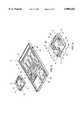
- FIG. 1illustrates a complete non-contact beam scanning data collection terminal housed in an industry standard PCMCIA card.
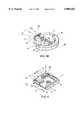
- FIG. 2shows a novel low profile scan engine adapted to fit into the beam scanning card terminal of FIG. 1.
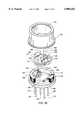
- FIG. 3illustrates details of the internal construction of an ultra thin scan engine similar to the module shown in FIG. 2.
- FIG. 4Aillustrates details of a preferred, low profile beam scan component.
- FIG. 4Bis another view of the thin profile beam scan component shown in FIG. 4A.
- FIG. 5illustrates a laser diode and focus element adapted for mounting in the scan module of FIG. 3.
- FIG. 6illustrates another embodiment, of an ultra thin scan module.
- FIG. 7illustrates a PCMCIA card scanner adapted for collection and loading of medical data.
- FIG. 8illustrates a method of rapidly scanning a bar code target without the need for aiming.
- FIG. 9illustrates a scan module which fits into a PCMCIA card as a module.
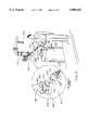
- FIG. 10is an exploded view of a non-contact scan system enclosable in a miniature housing similar to a TO-5 can which may be sealed against harsh environments.
- FIG. 11illustrates a low profile shaftless scan element which may scan in one or more dimensions.
- FIG. 12illustrates a bar code reading gas sampling probe and an omni directional readable barcode tag.
- FIG. 13illustrates a narrow profile lens holder and focusing system.
- FIG. 14illustrates a single piece lens holder mounted to a laser diode.
- FIG. 15illustrates a laser focus device of FIG. 14 spring loaded to a circuit board.
- FIG. 1shows a general layout of the integrated bar code scanning PCMCIA card scanner 30 of the present invention.
- the dimensions of the cardare defined by international standards and for a type I PCMCIA card which is the thinnest of such cards, its thickness T, is typically 3.3 millimeters whereas the length L, is 85.6 mm and the width W, is 54 mm. It should be noted that type II and type III cards are slightly thicker.
- a novel low profile scan module 2is secured to the plastic frame 6 of the card by a mounting feature 4. When scan module 2 is energized, a scanning beam is emitted through port 11 and scans a beam through a scan angle 8.
- port 13includes an optical filter 10 so that light of unwanted wavelengths is rejected before reaching photo detector 12 which converts the signals from the target into electric signals.
- the electric signalsare then processed by electronic circuits on thin circuit card 19 and information from the target is stored in memory devices such as memory element 16 which may be a non-volatile RAM.
- a clock battery 18supplies power continuously to a C-MOS clock circuit so that a time may be assigned to collected data if desired.
- a larger cell 20, typically a Lithium coin cellpowers scan module 2 and the data processing circuits. Cell 20 itself is installed into a user replaceable module 22.
- a female electrical connector 24is provided for inputting special data or instructions, up or down loading information or powering the card depending on the application.
- Port 26is provided as an auxiliary data port for inputting special data from accessories, uploading or downloading information especially when it is desired to reduce wear and tear on connector 24.
- Other portssuch as port 26 may be adapted for optical couplers, an ultrasonic transmitter/receiver, a fiber optic input/output, or a sub miniature power input for powering the device externally or for charging a cell and the like.
- the module 2consists of a solid state laser assembly 32, a micro lens 34 such as a gradient index (GRIN) lens which is available in sizes on the order of 1 mm diameter, a mirror 38 for directing the beam from the laser to a scan mirror 40 attached to moveable core 45 for directing and scanning the beam out of port 11.
- a second port 13allows reflected light to enter optical filter 10 which has photo detector 12 behind it.
- the scan mirror 40is part of the inventive ultra thin scan mechanism 52 of FIG. 4A the present invention. It should be noted that mirror 38 is optional in that it merely allows for the specific optical layout described in FIG. 3 but the light beam from the laser could have been aimed directly at mirror 40.
- FIG. 4Aa preferred low profile scan mechanism for the scan card is depicted with a ferromagnetic core 46, typically made from soft iron having a thickness of about 1.5 mm and pole faces A and B.
- Core 46has a small permanent magnet 50 which is about 3/10 mm thick mounted at its center.
- One of the poles of magnet 50is ideally in contact with core 46 while its opposite pole C faces permanent magnet 47 which is installed in rotor 45.
- Magnet 50creates an equal bias field of the same polarity which emanates from both poles A and B. For example if pole C of magnet 50 is south then poles A and B of core 46 will both be biased north.
- Winding 49is a winding 49.
- winding 49consists of about 800 turns of 48 gage wire and covers magnet 50.
- a preferred material for rotor 45is injection molded plastic with a low coefficient of friction.
- Rotor 45is typically about 1.5 mm high and can freely rotate on shaft 42.
- Permanent magnet 47is affixed to rotor 45 so that its pole face D has the same polarity as biased pole faces A and B of core 46.
- rotor 45tends to seek the position shown in FIG. 4 with magnet 47 pointing towards magnet 50 since pole face D of magnet 47 tends to be equally repelled by both poles A and B.
- magnet 47When coil 49 is energized with alternating current, pole faces A and B are magnetically modulated in an opposite sense causing an imbalance of the field between poles A and B, which interacts with magnet 47 causing rotor 45 to rotatably oscillate on shaft 42. Magnet 47 tracks the unbalanced field changes between poles A and B at the frequency of the alternating current. The direction of oscillation of rotor 47 is indicated by Arrow 43. The angle of oscillation of rotor 45 is generally proportional to the strength of the current supplied to coil 49 and the permanent magnetic bias field supplied by magnet 50 tends to return rotor 45 to its neutral position. Typically magnet 47 is a high energy magnet made from Neodymium-Iron-Boron alloy and is about 1 mm ⁇ 1 mm ⁇ 1.5 mm high.
- Shaft 42is preferably made from non-magnetic metal in order to minimize rotational friction between shaft 42, and rotor 45 and also to prevent magnetic field distortion.
- a short piece of polished Tungsten wire about 1/2 mm in diameterwas used for a shaft since even so called non-magnetic stainless steel was found to be magnetic enough to cause frictional and distortion problems.
- Mirror 40about 1.4 mm high ⁇ 3 mm long attached to rotor 45, causes the beam from path 36 to reflect along path 37 and scans the beam across a target as rotor 45 rotatably oscillates.
- the very small size and low friction of scan mechanism 52makes possible high frequency rates of operation at low power and wide angles especially when operated at resonance.
- the strength of magnet 50 in conjunction with the rotational inertia of rotor 45determines the resonant frequency of the scan element 44. (Increasing the strength of magnet 50 raises the resonant frequency of the scan element.) High speed operation on the order of several hundred scans per second is achievable due to the small mass of moving core 45.
- the high speed scangreatly increases the productivity of scanning data acquisition systems of the present invention and constitutes an important feature of the present invention especially in cases where non-contact scanning must be carried out rapidly enough to read irregular and even moving targets such as a patient's wrist band.
- a data capture sequence on the order of 1/10 second for the present inventionis thereby realized which dramatically conserves power of small batteries, reduces frustration and increases productivity.
- FIG. 10shows an exploded view of a completely self contained scan module packaged in a can type package.
- This compact scan modulecontains all the elements necessary for a moving beam scanner sealed into a miniature enclosure having a size on the order of a TO-5 transistor housing. As such this new scan sensor can operate in harsh environments such as in chemical leak detectors as will be described later.
- the components in the packageinclude a light source 104 such as a laser diode chip 104, a heat spreader/diode mount 102, a micro lens 114, above the laser emission source, a first mirror 112, a moveable mirror 109, a flexible mirror mount/suspension 108, a photo diode 106, a housing base 100, a housing cap 115, and a window 116.
- the assemblyis preferably enclosed and hermetically sealed.
- Drive coil 118serves to excite magnet 111 located preferably under mirror mount 129.
- the beam scanning mechanism of the scanneris essentially an axial scan element of the kind described in patent applications of which the instant application is a continuation-in-part.
- a coil-less version of the scan moduleis also contemplated in which the moving mirror element 109 is resonated by a piezeo bender wherein magnet 111 need not be affixed to the bottom of mirror mount 129.
- Micro lens 114can be a gradient index (GRIN) lens of the type manufactured by the Nippon Sheet Glass company.
- the lens 114may be optically cemented to the laser diode or mounted just above it.
- Photo detectoris preferably a PIN photo diode of the kind usually found in most laser diodes to monitor their power output however, this one is made larger, on the order of a few square millimeters.
- Diode 106serves two purposes: 1) to monitor the steady light output of the light source 104, 2) to receive modulated light back from the target scanned.
- Well known AC coupling and filter techniquesare used to separate the modulated, reflected light signal from the constant output of the light source 104. The signals may then be processed by external circuits.
- mirror 109moves to scan the outgoing beam accosts the target to be read, it also tracks the moving beam spot and reflects the modulated light from the target upon photo diode 106. This feature provides an efficient light collection method.
- a scanneris held, such as the one illustrated in FIG. 8, by a user whereupon s/he activates or "arms" the scanner with a key stroke or key stroke sequence. This could be two quick successive strokes of key 208 or a combination of key strokes. This wakes up appropriate data capture circuits such as a micro processor and arms the scan device making it sensitive to motion or the presence of a target, but the beam scan sequence is not yet begun. The user then quickly swipes the scanner past the general area in which the barcode to be read is located. The motion of this rapid swipe is sensed by a detector internally located within the scan terminal.
- Sensing of the motionthen activates a timing circuit for a time on the order of 1/10 of a second during which scanning at a rate of preferably 200 to 1000 scans per second commences. Only one set of data is allowed to be entered during the short scan sequence even though many successful scans may have occurred in rapid succession. (The techniques for preventing such multiple entries are well known.). Thus, 20 to 100 scans take place in 1/10 second, after which the laser, and scan device and other circuitry are automatically shut off. The scanner may still remain armed and ready for the next swipe. When the user no longer wishes to scan, a key stroke or combination of key strokes can be used to disarm the scanner so that further movement will not needlessly waste power.
- FIG. 8also illustrates an important aspect of the "credit card” form factor, wherein the scanner is configured generally as a rectangular prism of about several inches in length and width and substantially smaller in thickness, preferably less than about 1/2 inch and more preferably less than about 1/4 inch.
- the scannercan easily orient the scanner to the bar code to be read by bringing one dimension perpendicular to the bars of the bar code.
- the scannerPreferably as shown, the scanner generates scan lines in the plane of the scanner (i.e. in the plane defined by the length and width of the scanner.)
- the scannermay be turned on and operated in a continuously on mode while scanning target after target then turned off after the scan session is finished.
- this latter methodis not highly conservative of power it can be very productive when item after item is to be scanned such as at a check out counter or during inventory work.
- the latter type of scan initiatorutilizes a relative motion detector since it inherently responds only to relative motion between a detector and a target combination and not to vibration or inertial movement of the scanner itself.
- Various security alarm sensorsoperate in this manner in that they can detect the motion of a moving object in front them but if attached to an object such as a small appliance they can also detect they have been moved with respect to their surroundings.
- a preferred scan initiation/trigger method of the present inventionuses a relative motion detector of this kind to initiate the scan sequence in combination with high speed balanced scan devices and time-out circuits making them immune to false triggering caused by vibration while operating to conserve power and time.
- a power switch or "arming" switchsuch as switch 208 in FIG. 8.
- Thisactivates low power sleeping circuitry immediately prior to the actual scan sequence.
- the sleeping circuitryactivates the relative motion sensor circuit and may also activate sleeping data capture microprocessor circuitry making it ready to accept data.
- the userthen "swipes" the scanner 200 past general area 230 to be scanned without regard to the exact location of the target which may be a bar code target on a patient's wrist band 206 as shown in FIG. 7.
- the relative motion detector in the scannersenses relative movement of the target/scanner combination which causes internal circuitry to turn on the light beam and the high speed scan device momentarily for only a fraction of a second which may be on the order of 1/10 second thus conserving power.
- a tightly spaced raster pattern in area 230is created consisting of many closely spaced scan lines such as line 231.
- Preferably several hundred scan lines per secondare generated which are spaced so tightly that it is unlikely that the target will be missed.
- the data capture circuitryis programmed to only record one set of data per packet. A time lapse on the order of one second can be programmed into the data recording circuit before it can accept and record another element of data.
- the time out circuitdoes so. Once the data capture circuitry determines that the scan has been successfully recorded a beep can indicate that the data was captured whereupon the data processing circuit can go back to its sleep mode to save power.
- bottles bearing bar coded identification labelsmay be picked up and passed by a scanner such as that shown in FIG. 7.
- the labelis moved past the stationary scanner enabling the user to read display 204 which can confirm proper dosage, patient identity, special instructions or the like.
- the quickness of operation and power conservation benefitsare still preserved as shown by this example wherein the versatile benefits of the relative motion detection scan initiation method have been illustrated.
- ambient lightis available which is detectable by miniature photo detectors such as photo transistors, photo diodes, or photo resistors.
- a photo detectorforms the front end of a preferred relative motion detector by allowing it to drive a preamplifier circuit.
- a low power C-MOS amplifiercan be used for the photo detector preamplifier to conserve power.
- a current to voltage converteris a well known preamplifier circuit.
- the signal from the preamplifieris then fed through an appropriate filter such as a low pass, notch, or band pass filter circuit which is immune to the flicker of typical room lighting, which typically has a flicker rate of 120 Hz with a period of 8 ms. Only slower changes in received light are thus detected.
- an objectis passed or passes in front of the photo detector a change in reflected ambient light is registered. The amplitude of this rate of change of ambient light triggers a comparator which then automatically initiates the aforementioned scan cycle.
- the existing photo detector of the scanner itselfcan serve as the detector to register a change in the received ambient light to initiate a scan sequence.
- the ambient lightneed not be visible to the human eye.
- the methodmay be adapted to work with changes in infrared light which is radiated by all objects so that relative changes in received radiation may be detected.
- An infrared pass filtercan be used to enhance this sensor.
- scanned information signalsoccupy a particular band width (say 10 KHz and above) . If the detector of the scanner is swept past an object or if an object is moved in front of the detector while the internal light source of the scanner is on, then by using appropriate electronic filtering as previously described, the low frequency signal modulation received by the photo detector is then used to initiate the scan sequence by turning on the scan element, triggering the scanner, activating a microprocessor and the like in any combination desired.
- this methoduses slightly more power than the ambient light method it is well suited to applications where the ambient light is low such as in a darkened patient's room. Again use of electronic filters are employed to avoid false triggering due to ambient light flicker.
- a manual switchcan also be added to the scan device to turn all circuits off if long periods between usage is contemplated.
- Miniature Ultrasonic transmitter/receiver combinationsmay also be use to sense relative motion.
- the Panasonic companymakes a line of such ultrasonic components which may be used in toys and other products to activate them. These are employed in the same manner as the photo detectors for relative motion or proximity detectors except that sonic waves interacting with a target are detected and used to automatically trigger scan sequences.
- a novel sonic detectormay be incorporated into scanners of the present invention wherein a miniature microphone element is built into the scanner. Scanning is initiated by simply rubbing the scanner or tapping it so that a preset noise threshold is reached thereby initiating a timed scan sequence.
- This type scan actuatoris useful in industries where pipe couplings and valves are monitored for leakage. A person wearing protective work gloves and cannot easily pull a trigger. He may also have to climb ladders to get to a valve with a leak detector strapped to his body with a leak sniffing probe in one hand.
- the leak sniffing probecan have a barcode scan head attached to it as shown in FIG. 12. The user may then simply tap the probe near a bar coded identification tag on the valve to be sniffed to initiate the scan sequence. The valve identity is then logged in and the leak detection probe sniffs for a leak and that data is also logged into the terminal.
- Another method of sonic triggeringis to include a small moveable object which could rattle in the scanner.
- the previously mentioned microphone element in the housingwould hear the rattle and if sufficient movement of the scan head occurred the internal noise will rise above a set threshold to initiate scanning.
- This techniquecan work independently of gravity and can be set to have good immunity to false triggering.
- a very small tilt type switchsuch as a mercury switch has been found to work well as a scan initiation trigger when it changes state due to a change in orientation with respect to gravity or to acceleration and has been used to start a timed scan sequence.
- This type switchcan be positioned within a scanner to initiate scanning when the scanner is pointed downwards or swiped.
- a timer circuitmay be used in conjunction with the tilt switch to initiate a non-interrupt able scan sequence which terminates itself after a short predetermined time-out period to conserve power.
- a tilt switchallows operation of a scan head without the need for an external switch which may leak under water when a diver uses a scanner.
- the usermay "arm" the tilt detection circuit by touching a pad such as pad 208 in FIG. 7 so that when the scanner is tilted a short scan sequence is initiated.
- the circuitneed not be armed after each tilt but only once for a series of scannings.
- the arming switchmay then be turned off when the scanner is not in use to conserve power.
- a strain resistive element with a small mass attached to itcan also be set up as an acceleration detector as can a magnet and coil arrangement to sense acceleration. These can be employed in various permutations of scan initiation methods described above wherein one does not have to actuate a scanner with a trigger finger.
- the Honneywell companymakes semiconductor sensing integrated circuits which can sense extremely small changes in magnetic fields. These can sense small changes in their orientation with respect to the magnetic field of the earth or other magnetic objects like a compass producing an electronic output. With this kind of sensor any kind of change in position of the scanner can be made to initiate a scan.
- a hall sensor included in a scan headcan also be used to initiate operation of a scanner. If a level of security is needed the user may wear a magnetic ring on a finger which is brought into proximity within the area of the scanner containing the hall switch. This provides a somewhat obscure and uncommon method of initiating a data collection scan sequence to prevent accidental or unauthorized data entry and can also be sealed against harsh environments.
- the card scanner held as illustrated in FIG. 8,is ideal for close non-contact scanning of irregular objects subject to movement such as patients bar coded wrist band.
- Switch 208is provided on the device to activate sleeping circuitry prior to the actual scan sequence.
- the conveniently mounted switch 208may also have multiple positions for selecting various scan patterns and scan angles.
- One or combinations of the scan initiation trigger devices described in the present inventionmay be incorporated into a scanner to activate it automatically during use for special applications. Since the scan elements used in the scanners described herein consume very little power they can be operated from small batteries included in their housings for cordless operation.
- an optical link, 28 located at the back end of a card scanner shown in FIG. 1,is an ideal location for a typical data up/down load link.
- FIG. 7we see elements of a card scanner medical data collection system depicted.
- Scan terminal 200is in the form of a standard PCMCIA data collection card and is adapted for medical data entry.
- a patient's identification wrist band 206is read utilizing methods previously described.
- Several scan linesscan wrist band 206 to enter a patients identity which is presented on display 212 then entered by depressing a keypad key.
- a keypad keyPreferably when each piece of data is entered it is time and date tagged by an internal clock in the terminal.
- thermometer element 222can be plugged into terminal 200.
- Thermometer element 222is operated by pointing it into the ear of a patient and an actuator switch 224 on the terminal is momentarily pressed whereupon the patients temperature is read, and presented on display 212, then logged in by touching entry pad 208.
- Numerous companiesmake such infrared sensing thermometers.
- stethoscope 218can be plugged into the terminal such as stethoscope 218 to measure a patient's pulse or devices to measure blood pressure and other vital signs.
- stethoscope 218can be plugged into the terminal
- Several such miniature sensing elementsare now available which can be adapted to the inventive scan card terminal and it is possible to adapt such a terminal to plug into electrocardiogram equipment and digitally record a patients heart behavior.
- Lens mount 419is made from a single piece of material. Plastic or metal are suitable.
- the lens mountpreferably houses a small diameter gradient index lens 412.
- Lens 412is cemented into holder 419 by placing a liquid adhesive into area 406 whereby capillary action causes the adhesive to flow around the lens to hold it firmly in the holder.
- Two opposing slotssuch as slot 405 are incorporated into the body of lens holder 419.
- the slotsallow the thin wall lower body portion 418 of lens mount 419 to expand allowing mount 419 to grasp the top cap portion 422 of a commercial laser diode.(Although the base 424 of laser diodes are held to exacting tolerances the cap portions are notorious for their variation in diameter.)
- lens 412is cemented into mount 419 the assembly is pushed onto laser diode cap 422, focused and cemented to the laser diode cap with instant setting low viscosity adhesive such as a cyanoacrylate type.
- a groove 408is also provided in lens mount 419 to facilitate focusing just prior to bonding.
- FIG. 13a focus setup is depicted.
- a laser diode 423is firmly mounted in fixture 420 and powered through leads 426.
- a lens holder 414 with cemented lens 412is pressed onto laser cap 422.
- Lever arm 431has one end inserted into groove 408.
- the lever armpivots in fixed member 432 at fulcrum point 433.
- screw 442is turned the lever arm moves at end 435 according to direction arrows 434 thereby allowing precise positioning of the lens holder 414 with respect to laser cap 422. Bonding is then completed.
- This lens holder and focus methodis very low cost and low profile and allows the precise base 424 of the laser 423 to be free for mounting into other equipment.
- FIG. 15depicts the final mounting of the focused laser, mount, and lens into a heat sink 440. Since the base 424 of the laser has not been used as a reference to mount the lens holder as do prior art devices (such as described in U.S. Pat. Nos. 5,121,188 and 5,111,476), the entire assembly may be pushed into heat sink 440 with the diode base 424 in contact with the heat sink. A circuit board 450 with metalized contact areas 452, 454, and 456 is pushed into laser diode leads 426 with a force in direction F. A frame 460 is schematically depicted which holds the circuit board 450 fixed with respect to laser heat sink 440. This arrangement needs no solder since the laser leads 426 have spring qualities. A particular benefit of this assembly is that the focused laser assembly may be replaced in the field without a soldering iron.
Landscapes
- Physics & Mathematics (AREA)
- Engineering & Computer Science (AREA)
- Electromagnetism (AREA)
- General Physics & Mathematics (AREA)
- Artificial Intelligence (AREA)
- Toxicology (AREA)
- General Health & Medical Sciences (AREA)
- Computer Vision & Pattern Recognition (AREA)
- Health & Medical Sciences (AREA)
- Theoretical Computer Science (AREA)
- Optics & Photonics (AREA)
- Power Engineering (AREA)
- Image Input (AREA)
Abstract
Description
Claims (2)
Priority Applications (2)
| Application Number | Priority Date | Filing Date | Title |
|---|---|---|---|
| US08/910,257US5880452A (en) | 1990-11-15 | 1997-08-13 | Laser based PCMCIA data collection system with automatic triggering for portable applications and method of use |
| US09/203,715US6179444B1 (en) | 1990-11-15 | 1998-12-02 | Laser light source lens mount |
Applications Claiming Priority (8)
| Application Number | Priority Date | Filing Date | Title |
|---|---|---|---|
| US07/612,983US5187612A (en) | 1990-11-15 | 1990-11-15 | Gyrating programmable scanner |
| US08/006,754US5469291A (en) | 1990-11-15 | 1993-01-21 | Gyrating programmable scanner |
| US08/144,646US5506394A (en) | 1990-11-15 | 1993-10-28 | Light beam scanning pen, scan module for the device and method of utilization |
| US08/229,728US5550367A (en) | 1991-10-15 | 1994-04-19 | System for extending the operating range of a beam scanner |
| US08/273,101US5596442A (en) | 1990-11-15 | 1994-07-08 | Gyrating axial scanner |
| US08/332,629US5596446A (en) | 1990-11-15 | 1994-10-31 | Ultra compact scanning system for a wide range of speeds, angles and field depth |
| US48329995A | 1995-06-07 | 1995-06-07 | |
| US08/910,257US5880452A (en) | 1990-11-15 | 1997-08-13 | Laser based PCMCIA data collection system with automatic triggering for portable applications and method of use |
Related Parent Applications (2)
| Application Number | Title | Priority Date | Filing Date |
|---|---|---|---|
| US08/273,101Continuation-In-PartUS5596442A (en) | 1990-11-15 | 1994-07-08 | Gyrating axial scanner |
| US48329995AContinuation | 1990-11-15 | 1995-06-07 |
Related Child Applications (1)
| Application Number | Title | Priority Date | Filing Date |
|---|---|---|---|
| US09/203,715DivisionUS6179444B1 (en) | 1990-11-15 | 1998-12-02 | Laser light source lens mount |
Publications (1)
| Publication Number | Publication Date |
|---|---|
| US5880452Atrue US5880452A (en) | 1999-03-09 |
Family
ID=27567377
Family Applications (2)
| Application Number | Title | Priority Date | Filing Date |
|---|---|---|---|
| US08/910,257Expired - LifetimeUS5880452A (en) | 1990-11-15 | 1997-08-13 | Laser based PCMCIA data collection system with automatic triggering for portable applications and method of use |
| US09/203,715Expired - Fee RelatedUS6179444B1 (en) | 1990-11-15 | 1998-12-02 | Laser light source lens mount |
Family Applications After (1)
| Application Number | Title | Priority Date | Filing Date |
|---|---|---|---|
| US09/203,715Expired - Fee RelatedUS6179444B1 (en) | 1990-11-15 | 1998-12-02 | Laser light source lens mount |
Country Status (1)
| Country | Link |
|---|---|
| US (2) | US5880452A (en) |
Cited By (83)
| Publication number | Priority date | Publication date | Assignee | Title |
|---|---|---|---|---|
| US6036098A (en)* | 1992-05-15 | 2000-03-14 | Symbol Technologies, Inc. | Miniature scan element operably connected to a personal computer interface card |
| US6085975A (en)* | 1998-03-30 | 2000-07-11 | Disc, Inc. | Barcode module for an automated data storage library |
| US6290134B1 (en) | 1994-07-19 | 2001-09-18 | Psc Scanning, Inc. | Compact scanner module mountable to pointing instrument |
| US6305607B1 (en)* | 1990-05-29 | 2001-10-23 | Symbol Technologies, Inc. | Integrated bar code reader and RF transceiver |
| WO2002003320A1 (en)* | 2000-06-30 | 2002-01-10 | Motorola, Inc. | Electronically manipulated smartcard generating user comprehendible output |
| US6501973B1 (en) | 2000-06-30 | 2002-12-31 | Motorola, Inc. | Apparatus and method for measuring selected physical condition of an animate subject |
| US20030019934A1 (en)* | 1998-07-08 | 2003-01-30 | Hand Held Products, Inc. | Optical reader aiming assembly comprising aperture |
| US6522441B1 (en) | 2000-11-28 | 2003-02-18 | Psc Scanning, Inc. | Micro-optical system for an auto-focus scanner having an improved depth of field |
| US20030036217A1 (en)* | 2001-08-16 | 2003-02-20 | Motorola, Inc. | Microcavity semiconductor laser coupled to a waveguide |
| US6531740B2 (en) | 2001-07-17 | 2003-03-11 | Motorola, Inc. | Integrated impedance matching and stability network |
| US6536670B1 (en) | 1994-04-29 | 2003-03-25 | Psc Scanning, Inc. | PCMCIA interface card for coupling input devices such as barcode scanning engines to personal digital assistants and palmtop computers |
| US6555946B1 (en) | 2000-07-24 | 2003-04-29 | Motorola, Inc. | Acoustic wave device and process for forming the same |
| US20030089776A1 (en)* | 1999-10-04 | 2003-05-15 | Hand Held Products, Inc. | Optical reader comprising support post |
| US6585424B2 (en) | 2001-07-25 | 2003-07-01 | Motorola, Inc. | Structure and method for fabricating an electro-rheological lens |
| US20030121969A1 (en)* | 2001-12-06 | 2003-07-03 | John Wankmueller | Method and system for conducting transactions using a payment card with two technologies |
| US6590236B1 (en) | 2000-07-24 | 2003-07-08 | Motorola, Inc. | Semiconductor structure for use with high-frequency signals |
| US6589856B2 (en) | 2001-08-06 | 2003-07-08 | Motorola, Inc. | Method and apparatus for controlling anti-phase domains in semiconductor structures and devices |
| US6594414B2 (en) | 2001-07-25 | 2003-07-15 | Motorola, Inc. | Structure and method of fabrication for an optical switch |
| US6592031B1 (en)* | 1998-12-04 | 2003-07-15 | Stocko Contact Gmbh & Co. Kg | Authentication system for PC cards |
| WO2003060794A1 (en)* | 2002-01-04 | 2003-07-24 | Mastercard International Incorporated | Method and system for conducting transactions using a payment card with account information encoded in bar code |
| US6607131B1 (en)* | 1998-04-02 | 2003-08-19 | Datalogic S.P.A. | Reading method and reader for an optical code |
| US6639249B2 (en) | 2001-08-06 | 2003-10-28 | Motorola, Inc. | Structure and method for fabrication for a solid-state lighting device |
| US6638838B1 (en) | 2000-10-02 | 2003-10-28 | Motorola, Inc. | Semiconductor structure including a partially annealed layer and method of forming the same |
| US6637657B2 (en)* | 2001-04-06 | 2003-10-28 | Symbol Technologies, Inc. | Compact scan module with magnetically centered scan mirror |
| US6646293B2 (en) | 2001-07-18 | 2003-11-11 | Motorola, Inc. | Structure for fabricating high electron mobility transistors utilizing the formation of complaint substrates |
| US20030225623A1 (en)* | 2002-01-04 | 2003-12-04 | John Wankmueller | Method and system for conducting transactions using a payment card with account information encoded in bar code |
| US20030226895A1 (en)* | 2002-06-11 | 2003-12-11 | Hand Held Products, Inc. | Long range optical reader |
| US6667196B2 (en) | 2001-07-25 | 2003-12-23 | Motorola, Inc. | Method for real-time monitoring and controlling perovskite oxide film growth and semiconductor structure formed using the method |
| US6673667B2 (en) | 2001-08-15 | 2004-01-06 | Motorola, Inc. | Method for manufacturing a substantially integral monolithic apparatus including a plurality of semiconductor materials |
| US6673646B2 (en) | 2001-02-28 | 2004-01-06 | Motorola, Inc. | Growth of compound semiconductor structures on patterned oxide films and process for fabricating same |
| US6679429B2 (en)* | 2000-01-28 | 2004-01-20 | Olympus Optical Co., Ltd. | Bar code scanning device |
| US20040020990A1 (en)* | 2002-06-04 | 2004-02-05 | Havens William H. | Optical reader having a plurality of imaging modules |
| US6693033B2 (en) | 2000-02-10 | 2004-02-17 | Motorola, Inc. | Method of removing an amorphous oxide from a monocrystalline surface |
| US6693298B2 (en) | 2001-07-20 | 2004-02-17 | Motorola, Inc. | Structure and method for fabricating epitaxial semiconductor on insulator (SOI) structures and devices utilizing the formation of a compliant substrate for materials used to form same |
| US20040046031A1 (en)* | 1990-09-17 | 2004-03-11 | Metrologic Instruments, Inc. | Bar code scanning system with wireless communication links |
| US6709989B2 (en) | 2001-06-21 | 2004-03-23 | Motorola, Inc. | Method for fabricating a semiconductor structure including a metal oxide interface with silicon |
| US20040070312A1 (en)* | 2002-10-10 | 2004-04-15 | Motorola, Inc. | Integrated circuit and process for fabricating the same |
| US6729547B1 (en) | 2002-12-30 | 2004-05-04 | Motorola Inc. | System and method for interaction between an electronic writing device and a wireless device |
| US20040122746A1 (en)* | 2002-12-23 | 2004-06-24 | Charlier Michael L. | Method and system for direct purchase in response to a multi-media display |
| US20040149202A1 (en)* | 2000-02-10 | 2004-08-05 | Motorola, Inc. | Semiconductor structure, semiconductor device, communicating device, integrated circuit, and process for fabricating the same |
| US20040195328A1 (en)* | 1999-10-04 | 2004-10-07 | Welch Allyn Data Collection Inc. | Imaging module for optical reader |
| US20040217444A1 (en)* | 2001-10-17 | 2004-11-04 | Motorola, Inc. | Method and apparatus utilizing monocrystalline insulator |
| US6832725B2 (en) | 1999-10-04 | 2004-12-21 | Hand Held Products, Inc. | Optical reader comprising multiple color illumination |
| US6855992B2 (en) | 2001-07-24 | 2005-02-15 | Motorola Inc. | Structure and method for fabricating configurable transistor devices utilizing the formation of a compliant substrate for materials used to form the same |
| US20050039976A1 (en)* | 2003-08-18 | 2005-02-24 | Vu Vinh Thanh | Vibration-control platform |
| EP1274039A3 (en)* | 2001-07-03 | 2005-03-16 | Symbol Technologies, Inc. | Compact scan module with magnetically centered scan mirror |
| US6885065B2 (en) | 2002-11-20 | 2005-04-26 | Freescale Semiconductor, Inc. | Ferromagnetic semiconductor structure and method for forming the same |
| US6916717B2 (en) | 2002-05-03 | 2005-07-12 | Motorola, Inc. | Method for growing a monocrystalline oxide layer and for fabricating a semiconductor device on a monocrystalline substrate |
| US6965128B2 (en) | 2003-02-03 | 2005-11-15 | Freescale Semiconductor, Inc. | Structure and method for fabricating semiconductor microresonator devices |
| US20050279836A1 (en)* | 2002-06-04 | 2005-12-22 | Havens William H | Optical reader having a plurality of imaging modules |
| US6992321B2 (en) | 2001-07-13 | 2006-01-31 | Motorola, Inc. | Structure and method for fabricating semiconductor structures and devices utilizing piezoelectric materials |
| US20060022045A1 (en)* | 2004-07-15 | 2006-02-02 | Patrick Smets | Payment card signal characterization methods and circuits |
| US20060022033A1 (en)* | 2004-07-15 | 2006-02-02 | Patrick Smets | Method and system using a bitmap for passing contactless payment card transaction variables in standardized data formats |
| US7005717B2 (en) | 2000-05-31 | 2006-02-28 | Freescale Semiconductor, Inc. | Semiconductor device and method |
| US7020374B2 (en) | 2003-02-03 | 2006-03-28 | Freescale Semiconductor, Inc. | Optical waveguide structure and method for fabricating the same |
| US7019332B2 (en) | 2001-07-20 | 2006-03-28 | Freescale Semiconductor, Inc. | Fabrication of a wavelength locker within a semiconductor structure |
| US7045815B2 (en) | 2001-04-02 | 2006-05-16 | Freescale Semiconductor, Inc. | Semiconductor structure exhibiting reduced leakage current and method of fabricating same |
| US7090132B2 (en) | 2002-06-11 | 2006-08-15 | Hand Held Products, Inc. | Long range optical reader |
| US7105866B2 (en) | 2000-07-24 | 2006-09-12 | Freescale Semiconductor, Inc. | Heterojunction tunneling diodes and process for fabricating same |
| US20060252547A1 (en)* | 2000-05-01 | 2006-11-09 | Invoke Solutions, Inc. | Large Group Interactions |
| US20060259314A1 (en)* | 2003-09-22 | 2006-11-16 | Lilach Furman | Reading device |
| US20060267753A1 (en)* | 2005-05-31 | 2006-11-30 | Hussey Robert M | Bar coded wristband |
| US7161227B2 (en) | 2001-08-14 | 2007-01-09 | Motorola, Inc. | Structure and method for fabricating semiconductor structures and devices for detecting an object |
| US7169619B2 (en) | 2002-11-19 | 2007-01-30 | Freescale Semiconductor, Inc. | Method for fabricating semiconductor structures on vicinal substrates using a low temperature, low pressure, alkaline earth metal-rich process |
| US20070064920A1 (en)* | 2005-09-15 | 2007-03-22 | John Ruckart | Systems, methods and computer program products for aggregating contact information |
| US7203663B1 (en) | 2000-02-15 | 2007-04-10 | Jpmorgan Chase Bank, N.A. | System and method for converting information on paper forms to electronic data |
| US7211852B2 (en) | 2001-01-19 | 2007-05-01 | Freescale Semiconductor, Inc. | Structure and method for fabricating GaN devices utilizing the formation of a compliant substrate |
| US20070119947A1 (en)* | 2005-10-20 | 2007-05-31 | Blake Robert E | Scanner flipper integrity indicator |
| US7346174B1 (en)* | 1998-10-05 | 2008-03-18 | Clive Smith | Medical device with communication, measurement and data functions |
| US20080290170A1 (en)* | 2007-05-24 | 2008-11-27 | Blake Robert E | Scanner switched to active state by sensed movement in quiescent scanning mechanism |
| US20090224047A1 (en)* | 2008-03-05 | 2009-09-10 | Konica Minolta Systems Laboratory, Inc. | Contactless Scan Position Orientation Sensing |
| US7702538B2 (en) | 2000-08-01 | 2010-04-20 | Jpmorgan Chase Bank, N.A. | System and method for transponder-enabled account transactions |
| US20110069365A1 (en)* | 2009-09-23 | 2011-03-24 | Metrologic Instruments, Inc. | Scan element for use in scanning light and method of making the same |
| US8294969B2 (en) | 2009-09-23 | 2012-10-23 | Metrologic Instruments, Inc. | Scan element for use in scanning light and method of making the same |
| US8390909B2 (en) | 2009-09-23 | 2013-03-05 | Metrologic Instruments, Inc. | Molded elastomeric flexural elements for use in a laser scanning assemblies and scanners, and methods of manufacturing, tuning and adjusting the same |
| US8439271B2 (en) | 2004-07-15 | 2013-05-14 | Mastercard International Incorporated | Method and system using a bitmap for passing contactless payment card transaction variables in standardized data formats |
| US8770485B1 (en)* | 2013-06-28 | 2014-07-08 | Marson Technology Co., Ltd. | Actuation method of virtual laser barcode scanner |
| US8915439B2 (en) | 2012-02-06 | 2014-12-23 | Metrologic Instruments, Inc. | Laser scanning modules embodying silicone scan element with torsional hinges |
| EP3091456A1 (en)* | 2015-05-07 | 2016-11-09 | Deutsche Telekom AG | System for recording medical data |
| US10062254B1 (en)* | 2017-04-03 | 2018-08-28 | Alexander Paul | Intrusion detection system |
| US20220043255A1 (en)* | 2020-08-07 | 2022-02-10 | Mitsumi Electric Co., Ltd. | Rotary reciprocating drive actuator |
| US20220128410A1 (en)* | 2020-10-28 | 2022-04-28 | Datalogic I.P. Tech S.R.L. | Portable device combining indicia scan and contactless temperature functions |
| WO2024163712A1 (en)* | 2023-02-01 | 2024-08-08 | The Regents Of The University Of California | Autonomous vehicle-mounted sensing kit background |
Families Citing this family (9)
| Publication number | Priority date | Publication date | Assignee | Title |
|---|---|---|---|---|
| US6729543B1 (en)* | 1998-03-06 | 2004-05-04 | Audiovelocity, Inc. | Page identification system and method |
| DE10133567A1 (en) | 2001-07-13 | 2003-01-30 | Inficon Gmbh | Sniffing leak detector and method for its operation |
| JP4039039B2 (en)* | 2001-11-08 | 2008-01-30 | ソニー株式会社 | Personal authentication device |
| WO2005124949A1 (en)* | 2004-06-22 | 2005-12-29 | Hentze-Lissotschenko Patentverwaltungs Gmbh & Co. Kg | Laser device |
| DE102005009713A1 (en)* | 2005-03-03 | 2006-09-07 | Inficon Gmbh | Leak detector with sniffer probe |
| DE102005043494A1 (en) | 2005-09-13 | 2007-03-15 | Inficon Gmbh | Leak detector with sniffer probe |
| TWI269063B (en)* | 2005-12-23 | 2006-12-21 | E Pin Optical Industry Co Ltd | Laser device |
| US8157176B2 (en)* | 2007-05-25 | 2012-04-17 | Hewlett-Packard Development Company, L.P. | Modular marking apparatus and method |
| JP5703531B2 (en)* | 2011-03-23 | 2015-04-22 | スタンレー電気株式会社 | Vehicle lighting |
Citations (5)
| Publication number | Priority date | Publication date | Assignee | Title |
|---|---|---|---|---|
| US4922111A (en)* | 1987-11-20 | 1990-05-01 | Sanyo Electric Co., Ltd. | Card type image reader with means for relieving bending stress |
| US5189291A (en)* | 1989-05-01 | 1993-02-23 | Symbol Technologies, Inc. | Bar code reader operable as remote scanner or with fixed terminal |
| US5315097A (en)* | 1991-11-29 | 1994-05-24 | Ncr Corporation | Method and apparatus for operating a triggerless hand-held optical scanner |
| US5350909A (en)* | 1992-10-14 | 1994-09-27 | International Business Machines Corp. | Optical scanner for bar code scanning |
| US5468952A (en)* | 1992-05-15 | 1995-11-21 | Symbol Technologies, Inc. | Miniature high speed scan element mounted on a personal computer interface card |
Family Cites Families (5)
| Publication number | Priority date | Publication date | Assignee | Title |
|---|---|---|---|---|
| DE3413748A1 (en)* | 1984-04-12 | 1985-10-17 | Telefunken electronic GmbH, 7100 Heilbronn | OPTICAL SYSTEM |
| US4916579A (en)* | 1989-01-26 | 1990-04-10 | Murasa International | Gradient index zoom illuminator |
| US5307253A (en)* | 1992-12-09 | 1994-04-26 | Jehn E F | Structure of laser pointer |
| US5343376A (en)* | 1993-03-11 | 1994-08-30 | Huang Chao C | Structure of laser pointer |
| US5758950A (en)* | 1996-03-05 | 1998-06-02 | Ricoh Company, Ltd. | Light source device for an image forming apparatus |
- 1997
- 1997-08-13USUS08/910,257patent/US5880452A/ennot_activeExpired - Lifetime
- 1998
- 1998-12-02USUS09/203,715patent/US6179444B1/ennot_activeExpired - Fee Related
Patent Citations (5)
| Publication number | Priority date | Publication date | Assignee | Title |
|---|---|---|---|---|
| US4922111A (en)* | 1987-11-20 | 1990-05-01 | Sanyo Electric Co., Ltd. | Card type image reader with means for relieving bending stress |
| US5189291A (en)* | 1989-05-01 | 1993-02-23 | Symbol Technologies, Inc. | Bar code reader operable as remote scanner or with fixed terminal |
| US5315097A (en)* | 1991-11-29 | 1994-05-24 | Ncr Corporation | Method and apparatus for operating a triggerless hand-held optical scanner |
| US5468952A (en)* | 1992-05-15 | 1995-11-21 | Symbol Technologies, Inc. | Miniature high speed scan element mounted on a personal computer interface card |
| US5350909A (en)* | 1992-10-14 | 1994-09-27 | International Business Machines Corp. | Optical scanner for bar code scanning |
Cited By (135)
| Publication number | Priority date | Publication date | Assignee | Title |
|---|---|---|---|---|
| US6305607B1 (en)* | 1990-05-29 | 2001-10-23 | Symbol Technologies, Inc. | Integrated bar code reader and RF transceiver |
| US7040540B2 (en)* | 1990-09-17 | 2006-05-09 | Metrologic Instruments, Inc. | Bar code scanning system with wireless communication links |
| US20040046031A1 (en)* | 1990-09-17 | 2004-03-11 | Metrologic Instruments, Inc. | Bar code scanning system with wireless communication links |
| US6036098A (en)* | 1992-05-15 | 2000-03-14 | Symbol Technologies, Inc. | Miniature scan element operably connected to a personal computer interface card |
| US20040041029A1 (en)* | 1994-04-29 | 2004-03-04 | Psc Scanning, Inc. | PCMIA interface card for coupling input devices such as barcode scanning engines to personal digital assistants and palmtop computers |
| US6923377B2 (en) | 1994-04-29 | 2005-08-02 | Psc Inc. | PCMCIA interface card for coupling input devices such as barcode scanning engines to personal digital assistants and palmtop computers |
| US6536670B1 (en) | 1994-04-29 | 2003-03-25 | Psc Scanning, Inc. | PCMCIA interface card for coupling input devices such as barcode scanning engines to personal digital assistants and palmtop computers |
| US6290134B1 (en) | 1994-07-19 | 2001-09-18 | Psc Scanning, Inc. | Compact scanner module mountable to pointing instrument |
| US6572019B1 (en) | 1994-07-19 | 2003-06-03 | Psc Scanning, Inc. | Compact scanner module mountable to pointing instrument |
| US6085975A (en)* | 1998-03-30 | 2000-07-11 | Disc, Inc. | Barcode module for an automated data storage library |
| US6607131B1 (en)* | 1998-04-02 | 2003-08-19 | Datalogic S.P.A. | Reading method and reader for an optical code |
| US20030019934A1 (en)* | 1998-07-08 | 2003-01-30 | Hand Held Products, Inc. | Optical reader aiming assembly comprising aperture |
| US7346174B1 (en)* | 1998-10-05 | 2008-03-18 | Clive Smith | Medical device with communication, measurement and data functions |
| US6592031B1 (en)* | 1998-12-04 | 2003-07-15 | Stocko Contact Gmbh & Co. Kg | Authentication system for PC cards |
| US7533824B2 (en) | 1999-10-04 | 2009-05-19 | Hand Held Products, Inc. | Image sensor based optical reader |
| US20040195328A1 (en)* | 1999-10-04 | 2004-10-07 | Welch Allyn Data Collection Inc. | Imaging module for optical reader |
| US6832725B2 (en) | 1999-10-04 | 2004-12-21 | Hand Held Products, Inc. | Optical reader comprising multiple color illumination |
| US20070152055A1 (en)* | 1999-10-04 | 2007-07-05 | Barber Charles P | Imaging module for optical reader |
| US7500614B2 (en) | 1999-10-04 | 2009-03-10 | Hand Held Products, Inc. | Imaging module for optical reader |
| US9076054B2 (en) | 1999-10-04 | 2015-07-07 | Hand Held Products, Inc. | Image sensor based optical reader |
| US8474722B2 (en) | 1999-10-04 | 2013-07-02 | Hand Held Products, Inc. | Image sensor based optical reader |
| US20030089776A1 (en)* | 1999-10-04 | 2003-05-15 | Hand Held Products, Inc. | Optical reader comprising support post |
| US20110121076A1 (en)* | 1999-10-04 | 2011-05-26 | Hennick Robert J | Image sensor based optical reader |
| US7270274B2 (en) | 1999-10-04 | 2007-09-18 | Hand Held Products, Inc. | Imaging module comprising support post for optical reader |
| US7296751B2 (en)* | 1999-10-04 | 2007-11-20 | Hand Held Products, Inc. | Imaging module for optical reader |
| US20090236424A1 (en)* | 1999-10-04 | 2009-09-24 | Hand Held Products, Inc. | Image sensor based optical reader |
| US7878403B2 (en) | 1999-10-04 | 2011-02-01 | Hand Held Products, Inc. | Image sensor based optical reader |
| US6679429B2 (en)* | 2000-01-28 | 2004-01-20 | Olympus Optical Co., Ltd. | Bar code scanning device |
| US20040149202A1 (en)* | 2000-02-10 | 2004-08-05 | Motorola, Inc. | Semiconductor structure, semiconductor device, communicating device, integrated circuit, and process for fabricating the same |
| US6693033B2 (en) | 2000-02-10 | 2004-02-17 | Motorola, Inc. | Method of removing an amorphous oxide from a monocrystalline surface |
| US7067856B2 (en) | 2000-02-10 | 2006-06-27 | Freescale Semiconductor, Inc. | Semiconductor structure, semiconductor device, communicating device, integrated circuit, and process for fabricating the same |
| US20040232525A1 (en)* | 2000-02-10 | 2004-11-25 | Motorola, Inc. | Semiconductor structure, semiconductor device, communicating device, integrated circuit, and process for fabricating the same |
| US7203663B1 (en) | 2000-02-15 | 2007-04-10 | Jpmorgan Chase Bank, N.A. | System and method for converting information on paper forms to electronic data |
| US20060252547A1 (en)* | 2000-05-01 | 2006-11-09 | Invoke Solutions, Inc. | Large Group Interactions |
| US9925466B2 (en) | 2000-05-01 | 2018-03-27 | Invoke Solutions Inc. | Large group interactions |
| US8549076B2 (en) | 2000-05-01 | 2013-10-01 | Invoke Solutions Inc. | Large group interactions |
| US7005717B2 (en) | 2000-05-31 | 2006-02-28 | Freescale Semiconductor, Inc. | Semiconductor device and method |
| US6501973B1 (en) | 2000-06-30 | 2002-12-31 | Motorola, Inc. | Apparatus and method for measuring selected physical condition of an animate subject |
| WO2002003320A1 (en)* | 2000-06-30 | 2002-01-10 | Motorola, Inc. | Electronically manipulated smartcard generating user comprehendible output |
| US6590236B1 (en) | 2000-07-24 | 2003-07-08 | Motorola, Inc. | Semiconductor structure for use with high-frequency signals |
| US6555946B1 (en) | 2000-07-24 | 2003-04-29 | Motorola, Inc. | Acoustic wave device and process for forming the same |
| US7105866B2 (en) | 2000-07-24 | 2006-09-12 | Freescale Semiconductor, Inc. | Heterojunction tunneling diodes and process for fabricating same |
| US8781904B2 (en) | 2000-08-01 | 2014-07-15 | Jpmorgan Chase Bank, N.A. | System and method for transponder-enabled account transactions |
| US8781905B2 (en) | 2000-08-01 | 2014-07-15 | Jpmorgan Chase Bank, N.A. | System and method for transponder-enabled account transactions |
| US7702538B2 (en) | 2000-08-01 | 2010-04-20 | Jpmorgan Chase Bank, N.A. | System and method for transponder-enabled account transactions |
| US6638838B1 (en) | 2000-10-02 | 2003-10-28 | Motorola, Inc. | Semiconductor structure including a partially annealed layer and method of forming the same |
| US6522441B1 (en) | 2000-11-28 | 2003-02-18 | Psc Scanning, Inc. | Micro-optical system for an auto-focus scanner having an improved depth of field |
| US7211852B2 (en) | 2001-01-19 | 2007-05-01 | Freescale Semiconductor, Inc. | Structure and method for fabricating GaN devices utilizing the formation of a compliant substrate |
| US6673646B2 (en) | 2001-02-28 | 2004-01-06 | Motorola, Inc. | Growth of compound semiconductor structures on patterned oxide films and process for fabricating same |
| US7045815B2 (en) | 2001-04-02 | 2006-05-16 | Freescale Semiconductor, Inc. | Semiconductor structure exhibiting reduced leakage current and method of fabricating same |
| US6637657B2 (en)* | 2001-04-06 | 2003-10-28 | Symbol Technologies, Inc. | Compact scan module with magnetically centered scan mirror |
| US6709989B2 (en) | 2001-06-21 | 2004-03-23 | Motorola, Inc. | Method for fabricating a semiconductor structure including a metal oxide interface with silicon |
| EP1274039A3 (en)* | 2001-07-03 | 2005-03-16 | Symbol Technologies, Inc. | Compact scan module with magnetically centered scan mirror |
| US6992321B2 (en) | 2001-07-13 | 2006-01-31 | Motorola, Inc. | Structure and method for fabricating semiconductor structures and devices utilizing piezoelectric materials |
| US6531740B2 (en) | 2001-07-17 | 2003-03-11 | Motorola, Inc. | Integrated impedance matching and stability network |
| US6646293B2 (en) | 2001-07-18 | 2003-11-11 | Motorola, Inc. | Structure for fabricating high electron mobility transistors utilizing the formation of complaint substrates |
| US6693298B2 (en) | 2001-07-20 | 2004-02-17 | Motorola, Inc. | Structure and method for fabricating epitaxial semiconductor on insulator (SOI) structures and devices utilizing the formation of a compliant substrate for materials used to form same |
| US7019332B2 (en) | 2001-07-20 | 2006-03-28 | Freescale Semiconductor, Inc. | Fabrication of a wavelength locker within a semiconductor structure |
| US6855992B2 (en) | 2001-07-24 | 2005-02-15 | Motorola Inc. | Structure and method for fabricating configurable transistor devices utilizing the formation of a compliant substrate for materials used to form the same |
| US6594414B2 (en) | 2001-07-25 | 2003-07-15 | Motorola, Inc. | Structure and method of fabrication for an optical switch |
| US6585424B2 (en) | 2001-07-25 | 2003-07-01 | Motorola, Inc. | Structure and method for fabricating an electro-rheological lens |
| US6667196B2 (en) | 2001-07-25 | 2003-12-23 | Motorola, Inc. | Method for real-time monitoring and controlling perovskite oxide film growth and semiconductor structure formed using the method |
| US6589856B2 (en) | 2001-08-06 | 2003-07-08 | Motorola, Inc. | Method and apparatus for controlling anti-phase domains in semiconductor structures and devices |
| US6639249B2 (en) | 2001-08-06 | 2003-10-28 | Motorola, Inc. | Structure and method for fabrication for a solid-state lighting device |
| US7161227B2 (en) | 2001-08-14 | 2007-01-09 | Motorola, Inc. | Structure and method for fabricating semiconductor structures and devices for detecting an object |
| US6673667B2 (en) | 2001-08-15 | 2004-01-06 | Motorola, Inc. | Method for manufacturing a substantially integral monolithic apparatus including a plurality of semiconductor materials |
| US20030036217A1 (en)* | 2001-08-16 | 2003-02-20 | Motorola, Inc. | Microcavity semiconductor laser coupled to a waveguide |
| US20040217444A1 (en)* | 2001-10-17 | 2004-11-04 | Motorola, Inc. | Method and apparatus utilizing monocrystalline insulator |
| US7342276B2 (en) | 2001-10-17 | 2008-03-11 | Freescale Semiconductor, Inc. | Method and apparatus utilizing monocrystalline insulator |
| US20030121969A1 (en)* | 2001-12-06 | 2003-07-03 | John Wankmueller | Method and system for conducting transactions using a payment card with two technologies |
| US20050121512A1 (en)* | 2001-12-06 | 2005-06-09 | John Wankmueller | Method and system for conducting transactions using a payment card with two technologies |
| US7287695B2 (en) | 2001-12-06 | 2007-10-30 | Mastercard International Incorporated | Method and system for conducting transactions using a payment card with two technologies |
| US6857566B2 (en) | 2001-12-06 | 2005-02-22 | Mastercard International | Method and system for conducting transactions using a payment card with two technologies |
| US20030225623A1 (en)* | 2002-01-04 | 2003-12-04 | John Wankmueller | Method and system for conducting transactions using a payment card with account information encoded in bar code |
| WO2003060794A1 (en)* | 2002-01-04 | 2003-07-24 | Mastercard International Incorporated | Method and system for conducting transactions using a payment card with account information encoded in bar code |
| US6916717B2 (en) | 2002-05-03 | 2005-07-12 | Motorola, Inc. | Method for growing a monocrystalline oxide layer and for fabricating a semiconductor device on a monocrystalline substrate |
| US8074887B2 (en)* | 2002-06-04 | 2011-12-13 | Hand Held Products, Inc. | Optical reader having a plurality of imaging modules |
| US7219843B2 (en)* | 2002-06-04 | 2007-05-22 | Hand Held Products, Inc. | Optical reader having a plurality of imaging modules |
| US20040020990A1 (en)* | 2002-06-04 | 2004-02-05 | Havens William H. | Optical reader having a plurality of imaging modules |
| US20050279836A1 (en)* | 2002-06-04 | 2005-12-22 | Havens William H | Optical reader having a plurality of imaging modules |
| US20060255147A1 (en)* | 2002-06-11 | 2006-11-16 | Havens William H | Long range optical reader |
| US20030226895A1 (en)* | 2002-06-11 | 2003-12-11 | Hand Held Products, Inc. | Long range optical reader |
| US7090132B2 (en) | 2002-06-11 | 2006-08-15 | Hand Held Products, Inc. | Long range optical reader |
| US7055747B2 (en) | 2002-06-11 | 2006-06-06 | Hand Held Products, Inc. | Long range optical reader |
| US7389929B2 (en) | 2002-06-11 | 2008-06-24 | Hand Held Products, Inc. | Long range optical reader |
| US20040070312A1 (en)* | 2002-10-10 | 2004-04-15 | Motorola, Inc. | Integrated circuit and process for fabricating the same |
| US7169619B2 (en) | 2002-11-19 | 2007-01-30 | Freescale Semiconductor, Inc. | Method for fabricating semiconductor structures on vicinal substrates using a low temperature, low pressure, alkaline earth metal-rich process |
| US6885065B2 (en) | 2002-11-20 | 2005-04-26 | Freescale Semiconductor, Inc. | Ferromagnetic semiconductor structure and method for forming the same |
| US20040122746A1 (en)* | 2002-12-23 | 2004-06-24 | Charlier Michael L. | Method and system for direct purchase in response to a multi-media display |
| US6729547B1 (en) | 2002-12-30 | 2004-05-04 | Motorola Inc. | System and method for interaction between an electronic writing device and a wireless device |
| US6965128B2 (en) | 2003-02-03 | 2005-11-15 | Freescale Semiconductor, Inc. | Structure and method for fabricating semiconductor microresonator devices |
| US7020374B2 (en) | 2003-02-03 | 2006-03-28 | Freescale Semiconductor, Inc. | Optical waveguide structure and method for fabricating the same |
| US20050039976A1 (en)* | 2003-08-18 | 2005-02-24 | Vu Vinh Thanh | Vibration-control platform |
| EP1726092A4 (en)* | 2003-09-22 | 2011-07-13 | In Dot Ltd | Reading device |
| US20060259314A1 (en)* | 2003-09-22 | 2006-11-16 | Lilach Furman | Reading device |
| US7520435B2 (en) | 2004-07-15 | 2009-04-21 | Mastercard International Incorporated | Contactless payment card reader with a frusto-conical operating volume |
| US20080191031A1 (en)* | 2004-07-15 | 2008-08-14 | Patrick Smets | Reference equipment for testing contactless payment devices |
| US20060022043A1 (en)* | 2004-07-15 | 2006-02-02 | Patrick Smets | Contactless payment card reader with a frusto-conical operating volume |
| US20060027655A1 (en)* | 2004-07-15 | 2006-02-09 | Patrick Smets | Method and system for conducting contactless payment card transactions |
| US7431217B2 (en) | 2004-07-15 | 2008-10-07 | Mastercard International Incorporated | Reference equipment for testing contactless payment devices |
| US7669772B2 (en) | 2004-07-15 | 2010-03-02 | Mastercard International Incorporated | Method and system using a bitmap for passing contactless payment card transaction variables in standardized data formats |
| US7424977B2 (en) | 2004-07-15 | 2008-09-16 | Mastercard International Incorporated | Method and system for conducting contactless payment card transactions |
| US7717346B2 (en) | 2004-07-15 | 2010-05-18 | Mastercard International Incorporated | Collision detection and avoidance scheme for contactless card payment systems |
| US7775445B2 (en) | 2004-07-15 | 2010-08-17 | Mastercard International Incorporated | Reference equipment for testing contactless payment devices |
| US8439271B2 (en) | 2004-07-15 | 2013-05-14 | Mastercard International Incorporated | Method and system using a bitmap for passing contactless payment card transaction variables in standardized data formats |
| US20060022033A1 (en)* | 2004-07-15 | 2006-02-02 | Patrick Smets | Method and system using a bitmap for passing contactless payment card transaction variables in standardized data formats |
| US7422157B2 (en) | 2004-07-15 | 2008-09-09 | Mastercard International Incorporated | Payment card signal characterization methods and circuits |
| US20060022042A1 (en)* | 2004-07-15 | 2006-02-02 | Patrick Smets | Collision detection and avoidance scheme for contactless card payment systems |
| US20060022044A1 (en)* | 2004-07-15 | 2006-02-02 | Patrick Smets | Reference equipment for testing contactless payment devices |
| US20060022045A1 (en)* | 2004-07-15 | 2006-02-02 | Patrick Smets | Payment card signal characterization methods and circuits |
| US20110127325A1 (en)* | 2005-05-31 | 2011-06-02 | Hand Held Products, Inc. | System including bar coded wristband |
| US7849620B2 (en) | 2005-05-31 | 2010-12-14 | Hand Held Products, Inc. | Bar coded wristband |
| US20060267753A1 (en)* | 2005-05-31 | 2006-11-30 | Hussey Robert M | Bar coded wristband |
| US8556177B2 (en) | 2005-05-31 | 2013-10-15 | Hand Held Products, Inc. | System including bar coded wristband |
| US9491275B2 (en)* | 2005-09-15 | 2016-11-08 | AT&T Intellectual Property I, L.P., by transfer of ownership from AT&T | Systems, methods and computer program products for aggregating contact information |
| US20070064920A1 (en)* | 2005-09-15 | 2007-03-22 | John Ruckart | Systems, methods and computer program products for aggregating contact information |
| US20070119947A1 (en)* | 2005-10-20 | 2007-05-31 | Blake Robert E | Scanner flipper integrity indicator |
| US8002183B2 (en) | 2005-10-20 | 2011-08-23 | Metrologic Instruments, Inc. | Scanner flipper integrity indicator |
| US7832641B2 (en) | 2007-05-24 | 2010-11-16 | Metrologic Instruments, Inc. | Scanner switched to active state by sensed movement in quiescent scanning mechanism |
| US20080290170A1 (en)* | 2007-05-24 | 2008-11-27 | Blake Robert E | Scanner switched to active state by sensed movement in quiescent scanning mechanism |
| US20090224047A1 (en)* | 2008-03-05 | 2009-09-10 | Konica Minolta Systems Laboratory, Inc. | Contactless Scan Position Orientation Sensing |
| US8294969B2 (en) | 2009-09-23 | 2012-10-23 | Metrologic Instruments, Inc. | Scan element for use in scanning light and method of making the same |
| US8059324B2 (en) | 2009-09-23 | 2011-11-15 | Metrologic Instruments, Inc. | Scan element for use in scanning light and method of making the same |
| US20110069365A1 (en)* | 2009-09-23 | 2011-03-24 | Metrologic Instruments, Inc. | Scan element for use in scanning light and method of making the same |
| US8390909B2 (en) | 2009-09-23 | 2013-03-05 | Metrologic Instruments, Inc. | Molded elastomeric flexural elements for use in a laser scanning assemblies and scanners, and methods of manufacturing, tuning and adjusting the same |
| US9158951B2 (en) | 2012-02-06 | 2015-10-13 | Metrologic Instruments, Inc. | Laser scanning modules embodying silicone scan element with torsional hinges |
| US8915439B2 (en) | 2012-02-06 | 2014-12-23 | Metrologic Instruments, Inc. | Laser scanning modules embodying silicone scan element with torsional hinges |
| US8770485B1 (en)* | 2013-06-28 | 2014-07-08 | Marson Technology Co., Ltd. | Actuation method of virtual laser barcode scanner |
| EP3091456A1 (en)* | 2015-05-07 | 2016-11-09 | Deutsche Telekom AG | System for recording medical data |
| US10062254B1 (en)* | 2017-04-03 | 2018-08-28 | Alexander Paul | Intrusion detection system |
| US20220043255A1 (en)* | 2020-08-07 | 2022-02-10 | Mitsumi Electric Co., Ltd. | Rotary reciprocating drive actuator |
| US11936250B2 (en)* | 2020-08-07 | 2024-03-19 | Mitsumi Electric Co., Ltd. | Rotary reciprocating drive actuator |
| US20220128410A1 (en)* | 2020-10-28 | 2022-04-28 | Datalogic I.P. Tech S.R.L. | Portable device combining indicia scan and contactless temperature functions |
| US11906361B2 (en)* | 2020-10-28 | 2024-02-20 | Datalogic Ip Tech S.R.L. | Portable device combining indicia scan and contactless temperature functions |
| WO2024163712A1 (en)* | 2023-02-01 | 2024-08-08 | The Regents Of The University Of California | Autonomous vehicle-mounted sensing kit background |
Also Published As
| Publication number | Publication date |
|---|---|
| US6179444B1 (en) | 2001-01-30 |
Similar Documents
| Publication | Publication Date | Title |
|---|---|---|
| US5880452A (en) | Laser based PCMCIA data collection system with automatic triggering for portable applications and method of use | |
| US6057554A (en) | Reflective switch | |
| US5831261A (en) | Reflective switch | |
| US6202930B1 (en) | Low power pen shaped and wearable scan systems with ergonomic actuation | |
| US5422469A (en) | Fiber optic barcode readers using purely mechanical scanner oscillation | |
| US6572019B1 (en) | Compact scanner module mountable to pointing instrument | |
| US6641044B2 (en) | Light beam scanning pen, scan module for the device and method of utilization | |
| US5521367A (en) | Fiber optic barcode reader with piezoelectric element | |
| US5506394A (en) | Light beam scanning pen, scan module for the device and method of utilization | |
| US6247647B1 (en) | Scan pattern generator convertible between multiple and single line patterns | |
| US6311896B1 (en) | Compact bar code scanner | |
| EP0433593B1 (en) | Bar code symbol readers with edge enhancement | |
| US5693929A (en) | Scanning module with spring made resistant to overflexing | |
| JP3210668B2 (en) | Electro-optical scanning system | |
| US5436440A (en) | Digitizing circuit for a laser scanner using digital and synchronizing signals | |
| US6375079B1 (en) | Portable optical scanning and pointing systems | |
| US5661290A (en) | Scanner with flexibly supported light emitter | |
| WO1990009007A1 (en) | Data acquisition system with laser scanner module | |
| US6491225B1 (en) | Electro-optical reader with electronic stylus | |
| US20020092913A1 (en) | Flexible battery and band for user supported module | |
| TWI245224B (en) | Scan module for use in a reader for electro-optically reading indicia and arrangement for centering an oscillatable scan mirror in a rest position in a reader for electro-optically reading indicia | |
| CA2341449C (en) | Compact bar code scanner | |
| JPH08263581A (en) | Optical system and optical pointer module | |
| CN220085389U (en) | Scanning device | |
| AU2925102A (en) | Compact bar code scanner |
Legal Events
| Date | Code | Title | Description |
|---|---|---|---|
| STCF | Information on status: patent grant | Free format text:PATENTED CASE | |
| AS | Assignment | Owner name:GEO ACQUISITION CORP., NEW YORK Free format text:ASSIGNMENT OF ASSIGNORS INTEREST;ASSIGNOR:GEO LABS, INC.;REEL/FRAME:010795/0272 Effective date:19991221 | |
| AS | Assignment | Owner name:PSC, INC., NEW YORK Free format text:ASSIGNMENT OF ASSIGNORS INTEREST;ASSIGNOR:GEO LABS, INC.;REEL/FRAME:011979/0130 Effective date:19991221 | |
| AS | Assignment | Owner name:PSC, INC., NEW YORK Free format text:RE-RECORD TO CORRECT THE RECORDATE DATE OF 07-20-2000 TO 07-20-2001 PREVIOUSLY RECORDED AT REEL 011979 FRAME 0130. (ASSIGNMENT OF ASSIGNOR'S INTEREST) OR NATURE OF CONVEYANCE;ASSIGNOR:GEO LABS, INC.;REEL/FRAME:012312/0059 Effective date:19991221 Owner name:SYMBOL TECHNOLOGIES, INC., NEW YORK Free format text:ASSIGNMENT OF ASSIGNORS INTEREST;ASSIGNOR:PSC, INC.;REEL/FRAME:011996/0129 Effective date:20001001 | |
| FEPP | Fee payment procedure | Free format text:PAT HOLDER NO LONGER CLAIMS SMALL ENTITY STATUS, ENTITY STATUS SET TO UNDISCOUNTED (ORIGINAL EVENT CODE: STOL); ENTITY STATUS OF PATENT OWNER: LARGE ENTITY | |
| REFU | Refund | Free format text:REFUND - SURCHARGE, PETITION TO ACCEPT PYMT AFTER EXP, UNINTENTIONAL (ORIGINAL EVENT CODE: R2551); ENTITY STATUS OF PATENT OWNER: LARGE ENTITY | |
| FPAY | Fee payment | Year of fee payment:4 | |
| AS | Assignment | Owner name:JPMORGAN CHASE BANK, N.A., NEW YORK Free format text:SECURITY INTEREST;ASSIGNOR:SYMBOL TECHNOLOGIES, INC.;REEL/FRAME:016116/0203 Effective date:20041229 | |
| FPAY | Fee payment | Year of fee payment:8 | |
| FPAY | Fee payment | Year of fee payment:12 |