US5877874A - Device for concentrating optical radiation - Google Patents
Device for concentrating optical radiationDownload PDFInfo
- Publication number
- US5877874A US5877874AUS08/897,068US89706897AUS5877874AUS 5877874 AUS5877874 AUS 5877874AUS 89706897 AUS89706897 AUS 89706897AUS 5877874 AUS5877874 AUS 5877874A
- Authority
- US
- United States
- Prior art keywords
- holographic
- multiplexed
- transparent plate
- highly transparent
- planar
- Prior art date
- Legal status (The legal status is an assumption and is not a legal conclusion. Google has not performed a legal analysis and makes no representation as to the accuracy of the status listed.)
- Expired - Lifetime
Links
Images


Classifications
- C—CHEMISTRY; METALLURGY
- C09—DYES; PAINTS; POLISHES; NATURAL RESINS; ADHESIVES; COMPOSITIONS NOT OTHERWISE PROVIDED FOR; APPLICATIONS OF MATERIALS NOT OTHERWISE PROVIDED FOR
- C09B—ORGANIC DYES OR CLOSELY-RELATED COMPOUNDS FOR PRODUCING DYES, e.g. PIGMENTS; MORDANTS; LAKES
- C09B47/00—Porphines; Azaporphines
- C09B47/04—Phthalocyanines abbreviation: Pc
- C09B47/06—Preparation from carboxylic acids or derivatives thereof, e.g. anhydrides, amides, mononitriles, phthalimide, o-cyanobenzamide
- C09B47/067—Preparation from carboxylic acids or derivatives thereof, e.g. anhydrides, amides, mononitriles, phthalimide, o-cyanobenzamide from phthalodinitriles naphthalenedinitriles, aromatic dinitriles prepared in situ, hydrogenated phthalodinitrile
- G—PHYSICS
- G02—OPTICS
- G02B—OPTICAL ELEMENTS, SYSTEMS OR APPARATUS
- G02B5/00—Optical elements other than lenses
- G02B5/32—Holograms used as optical elements
- C—CHEMISTRY; METALLURGY
- C09—DYES; PAINTS; POLISHES; NATURAL RESINS; ADHESIVES; COMPOSITIONS NOT OTHERWISE PROVIDED FOR; APPLICATIONS OF MATERIALS NOT OTHERWISE PROVIDED FOR
- C09B—ORGANIC DYES OR CLOSELY-RELATED COMPOUNDS FOR PRODUCING DYES, e.g. PIGMENTS; MORDANTS; LAKES
- C09B47/00—Porphines; Azaporphines
- C09B47/04—Phthalocyanines abbreviation: Pc
- C09B47/08—Preparation from other phthalocyanine compounds, e.g. cobaltphthalocyanineamine complex
- C09B47/085—Preparation from other phthalocyanine compounds, e.g. cobaltphthalocyanineamine complex substituting the central metal atom
- C—CHEMISTRY; METALLURGY
- C09—DYES; PAINTS; POLISHES; NATURAL RESINS; ADHESIVES; COMPOSITIONS NOT OTHERWISE PROVIDED FOR; APPLICATIONS OF MATERIALS NOT OTHERWISE PROVIDED FOR
- C09B—ORGANIC DYES OR CLOSELY-RELATED COMPOUNDS FOR PRODUCING DYES, e.g. PIGMENTS; MORDANTS; LAKES
- C09B67/00—Influencing the physical, e.g. the dyeing or printing properties of dyestuffs without chemical reactions, e.g. by treating with solvents grinding or grinding assistants, coating of pigments or dyes; Process features in the making of dyestuff preparations; Dyestuff preparations of a special physical nature, e.g. tablets, films
- C09B67/0001—Post-treatment of organic pigments or dyes
- C09B67/0014—Influencing the physical properties by treatment with a liquid, e.g. solvents
- C09B67/0016—Influencing the physical properties by treatment with a liquid, e.g. solvents of phthalocyanines
- C—CHEMISTRY; METALLURGY
- C09—DYES; PAINTS; POLISHES; NATURAL RESINS; ADHESIVES; COMPOSITIONS NOT OTHERWISE PROVIDED FOR; APPLICATIONS OF MATERIALS NOT OTHERWISE PROVIDED FOR
- C09B—ORGANIC DYES OR CLOSELY-RELATED COMPOUNDS FOR PRODUCING DYES, e.g. PIGMENTS; MORDANTS; LAKES
- C09B67/00—Influencing the physical, e.g. the dyeing or printing properties of dyestuffs without chemical reactions, e.g. by treating with solvents grinding or grinding assistants, coating of pigments or dyes; Process features in the making of dyestuff preparations; Dyestuff preparations of a special physical nature, e.g. tablets, films
- C09B67/0001—Post-treatment of organic pigments or dyes
- C09B67/0017—Influencing the physical properties by treatment with an acid, H2SO4
- C09B67/0019—Influencing the physical properties by treatment with an acid, H2SO4 of phthalocyanines
- C—CHEMISTRY; METALLURGY
- C09—DYES; PAINTS; POLISHES; NATURAL RESINS; ADHESIVES; COMPOSITIONS NOT OTHERWISE PROVIDED FOR; APPLICATIONS OF MATERIALS NOT OTHERWISE PROVIDED FOR
- C09B—ORGANIC DYES OR CLOSELY-RELATED COMPOUNDS FOR PRODUCING DYES, e.g. PIGMENTS; MORDANTS; LAKES
- C09B67/00—Influencing the physical, e.g. the dyeing or printing properties of dyestuffs without chemical reactions, e.g. by treating with solvents grinding or grinding assistants, coating of pigments or dyes; Process features in the making of dyestuff preparations; Dyestuff preparations of a special physical nature, e.g. tablets, films
- C09B67/0001—Post-treatment of organic pigments or dyes
- C09B67/0022—Wet grinding of pigments
- C09B67/0023—Wet grinding of pigments of phthalocyanines
- C—CHEMISTRY; METALLURGY
- C09—DYES; PAINTS; POLISHES; NATURAL RESINS; ADHESIVES; COMPOSITIONS NOT OTHERWISE PROVIDED FOR; APPLICATIONS OF MATERIALS NOT OTHERWISE PROVIDED FOR
- C09B—ORGANIC DYES OR CLOSELY-RELATED COMPOUNDS FOR PRODUCING DYES, e.g. PIGMENTS; MORDANTS; LAKES
- C09B67/00—Influencing the physical, e.g. the dyeing or printing properties of dyestuffs without chemical reactions, e.g. by treating with solvents grinding or grinding assistants, coating of pigments or dyes; Process features in the making of dyestuff preparations; Dyestuff preparations of a special physical nature, e.g. tablets, films
- C09B67/0025—Crystal modifications; Special X-ray patterns
- C09B67/0026—Crystal modifications; Special X-ray patterns of phthalocyanine pigments
- F—MECHANICAL ENGINEERING; LIGHTING; HEATING; WEAPONS; BLASTING
- F24—HEATING; RANGES; VENTILATING
- F24S—SOLAR HEAT COLLECTORS; SOLAR HEAT SYSTEMS
- F24S23/00—Arrangements for concentrating solar-rays for solar heat collectors
- F—MECHANICAL ENGINEERING; LIGHTING; HEATING; WEAPONS; BLASTING
- F24—HEATING; RANGES; VENTILATING
- F24S—SOLAR HEAT COLLECTORS; SOLAR HEAT SYSTEMS
- F24S50/00—Arrangements for controlling solar heat collectors
- F24S50/20—Arrangements for controlling solar heat collectors for tracking
- G—PHYSICS
- G03—PHOTOGRAPHY; CINEMATOGRAPHY; ANALOGOUS TECHNIQUES USING WAVES OTHER THAN OPTICAL WAVES; ELECTROGRAPHY; HOLOGRAPHY
- G03G—ELECTROGRAPHY; ELECTROPHOTOGRAPHY; MAGNETOGRAPHY
- G03G5/00—Recording members for original recording by exposure, e.g. to light, to heat, to electrons; Manufacture thereof; Selection of materials therefor
- G03G5/02—Charge-receiving layers
- G03G5/04—Photoconductive layers; Charge-generation layers or charge-transporting layers; Additives therefor; Binders therefor
- G03G5/06—Photoconductive layers; Charge-generation layers or charge-transporting layers; Additives therefor; Binders therefor characterised by the photoconductive material being organic
- G03G5/0664—Dyes
- G03G5/0696—Phthalocyanines
- H—ELECTRICITY
- H10—SEMICONDUCTOR DEVICES; ELECTRIC SOLID-STATE DEVICES NOT OTHERWISE PROVIDED FOR
- H10F—INORGANIC SEMICONDUCTOR DEVICES SENSITIVE TO INFRARED RADIATION, LIGHT, ELECTROMAGNETIC RADIATION OF SHORTER WAVELENGTH OR CORPUSCULAR RADIATION
- H10F77/00—Constructional details of devices covered by this subclass
- H10F77/40—Optical elements or arrangements
- H10F77/42—Optical elements or arrangements directly associated or integrated with photovoltaic cells, e.g. light-reflecting means or light-concentrating means
- H10F77/45—Wavelength conversion means, e.g. by using luminescent material, fluorescent concentrators or up-conversion arrangements
- H—ELECTRICITY
- H10—SEMICONDUCTOR DEVICES; ELECTRIC SOLID-STATE DEVICES NOT OTHERWISE PROVIDED FOR
- H10F—INORGANIC SEMICONDUCTOR DEVICES SENSITIVE TO INFRARED RADIATION, LIGHT, ELECTROMAGNETIC RADIATION OF SHORTER WAVELENGTH OR CORPUSCULAR RADIATION
- H10F77/00—Constructional details of devices covered by this subclass
- H10F77/40—Optical elements or arrangements
- H10F77/42—Optical elements or arrangements directly associated or integrated with photovoltaic cells, e.g. light-reflecting means or light-concentrating means
- H10F77/484—Refractive light-concentrating means, e.g. lenses
- H—ELECTRICITY
- H10—SEMICONDUCTOR DEVICES; ELECTRIC SOLID-STATE DEVICES NOT OTHERWISE PROVIDED FOR
- H10F—INORGANIC SEMICONDUCTOR DEVICES SENSITIVE TO INFRARED RADIATION, LIGHT, ELECTROMAGNETIC RADIATION OF SHORTER WAVELENGTH OR CORPUSCULAR RADIATION
- H10F77/00—Constructional details of devices covered by this subclass
- H10F77/40—Optical elements or arrangements
- H10F77/42—Optical elements or arrangements directly associated or integrated with photovoltaic cells, e.g. light-reflecting means or light-concentrating means
- H10F77/488—Reflecting light-concentrating means, e.g. parabolic mirrors or concentrators using total internal reflection
- Y—GENERAL TAGGING OF NEW TECHNOLOGICAL DEVELOPMENTS; GENERAL TAGGING OF CROSS-SECTIONAL TECHNOLOGIES SPANNING OVER SEVERAL SECTIONS OF THE IPC; TECHNICAL SUBJECTS COVERED BY FORMER USPC CROSS-REFERENCE ART COLLECTIONS [XRACs] AND DIGESTS
- Y02—TECHNOLOGIES OR APPLICATIONS FOR MITIGATION OR ADAPTATION AGAINST CLIMATE CHANGE
- Y02B—CLIMATE CHANGE MITIGATION TECHNOLOGIES RELATED TO BUILDINGS, e.g. HOUSING, HOUSE APPLIANCES OR RELATED END-USER APPLICATIONS
- Y02B10/00—Integration of renewable energy sources in buildings
- Y02B10/10—Photovoltaic [PV]
- Y—GENERAL TAGGING OF NEW TECHNOLOGICAL DEVELOPMENTS; GENERAL TAGGING OF CROSS-SECTIONAL TECHNOLOGIES SPANNING OVER SEVERAL SECTIONS OF THE IPC; TECHNICAL SUBJECTS COVERED BY FORMER USPC CROSS-REFERENCE ART COLLECTIONS [XRACs] AND DIGESTS
- Y02—TECHNOLOGIES OR APPLICATIONS FOR MITIGATION OR ADAPTATION AGAINST CLIMATE CHANGE
- Y02B—CLIMATE CHANGE MITIGATION TECHNOLOGIES RELATED TO BUILDINGS, e.g. HOUSING, HOUSE APPLIANCES OR RELATED END-USER APPLICATIONS
- Y02B10/00—Integration of renewable energy sources in buildings
- Y02B10/20—Solar thermal
- Y—GENERAL TAGGING OF NEW TECHNOLOGICAL DEVELOPMENTS; GENERAL TAGGING OF CROSS-SECTIONAL TECHNOLOGIES SPANNING OVER SEVERAL SECTIONS OF THE IPC; TECHNICAL SUBJECTS COVERED BY FORMER USPC CROSS-REFERENCE ART COLLECTIONS [XRACs] AND DIGESTS
- Y02—TECHNOLOGIES OR APPLICATIONS FOR MITIGATION OR ADAPTATION AGAINST CLIMATE CHANGE
- Y02E—REDUCTION OF GREENHOUSE GAS [GHG] EMISSIONS, RELATED TO ENERGY GENERATION, TRANSMISSION OR DISTRIBUTION
- Y02E10/00—Energy generation through renewable energy sources
- Y02E10/40—Solar thermal energy, e.g. solar towers
- Y02E10/44—Heat exchange systems
- Y—GENERAL TAGGING OF NEW TECHNOLOGICAL DEVELOPMENTS; GENERAL TAGGING OF CROSS-SECTIONAL TECHNOLOGIES SPANNING OVER SEVERAL SECTIONS OF THE IPC; TECHNICAL SUBJECTS COVERED BY FORMER USPC CROSS-REFERENCE ART COLLECTIONS [XRACs] AND DIGESTS
- Y02—TECHNOLOGIES OR APPLICATIONS FOR MITIGATION OR ADAPTATION AGAINST CLIMATE CHANGE
- Y02E—REDUCTION OF GREENHOUSE GAS [GHG] EMISSIONS, RELATED TO ENERGY GENERATION, TRANSMISSION OR DISTRIBUTION
- Y02E10/00—Energy generation through renewable energy sources
- Y02E10/40—Solar thermal energy, e.g. solar towers
- Y02E10/47—Mountings or tracking
- Y—GENERAL TAGGING OF NEW TECHNOLOGICAL DEVELOPMENTS; GENERAL TAGGING OF CROSS-SECTIONAL TECHNOLOGIES SPANNING OVER SEVERAL SECTIONS OF THE IPC; TECHNICAL SUBJECTS COVERED BY FORMER USPC CROSS-REFERENCE ART COLLECTIONS [XRACs] AND DIGESTS
- Y02—TECHNOLOGIES OR APPLICATIONS FOR MITIGATION OR ADAPTATION AGAINST CLIMATE CHANGE
- Y02E—REDUCTION OF GREENHOUSE GAS [GHG] EMISSIONS, RELATED TO ENERGY GENERATION, TRANSMISSION OR DISTRIBUTION
- Y02E10/00—Energy generation through renewable energy sources
- Y02E10/50—Photovoltaic [PV] energy
- Y02E10/52—PV systems with concentrators
Definitions
- the present inventionrelates to optics, particularly to the field of optical concentrators for gathering optical radiation.
- the optical concentrator made by the subject of the present inventionmay be used in all technical areas where concentrated optical radiation is utilized. It can be used for optical radiation spanning the spectrum from the ultra-violet to the infrared.
- Luminescent solar concentratorsare known in the art and act to trap and collect light from luminescent centers dispersed in a planar sheet. Luminescent concentrators utilize the total internal reflection in the wave-guide to trap a portion of the light emitted from the luminescent centers. The luminescent centers reradiate longer wavelength light in a 360 degree solid angle and so are inefficient in directing light to one edge of the plate or to a small region of the edge.
- a solar concentratorutilizes a hologram and a prism or plate; see, e.g., U.S. Pat. No. 4,863,224, issued to Afian et al.
- this solar concentratorneeds to be aligned to the sun and does not provide for any passive solar tracking ability.
- a light gathering devicecomprising a hologram and a total reflection surface for a collecting monochromatic light at a single angle of incidence; see, e.g., U.S. Pat. No. 5,268,985, issued to Ando et al.
- Ando et alemploy a single angle of incidence and a single wavelength, and thus require a tracking mechanism and cannot utilized the entire solar spectrum.
- an electromagnetic wave concentratorsee, e.g., U.S. Pat. No. 4,505,264, issued to Tremblay.
- the electromagnetic wave concentratorutilizes a multidielectric guiding plate to concentrate electromagnetic energy.
- This inventionhas the disadvantage of multiple reflection losses in the guiding plate and high absorption losses in some of the more cost effective embodiments. Also this invention posses difficult optical fabrication problems and hence is more expensive to fabricate.
- Each application disclosed hereinhas a unique spectral requirement to work effectively.
- a holographic planar concentratorfor collecting and concentrating optical radiation.
- the holographic planar concentratorcomprises a planar highly transparent plate and at least one multiplexed holographic optical film mounted on a surface thereof to form a light guiding structure.
- the multiplexed holographic optical filmhas recorded therein a plurality of diffractive structures having two or more regions which are angularly and spectrally multiplexed.
- the multiplexed hologramis adapted to couple optical radiation into the planar highly transparent plate such that the optical radiation is not lost and travels through both the planar highly transparent plate and the multiplexed holographic film.
- the multiplexing of the hologramserves to reduce recoupling losses in the holographic planar concentrator.
- the highly transparent plateis multifunctional and performs in the following manner. First, it acts as a structural support for the holographic material. Second, it provides environmental protection to the holographic material. Third, it provides high optical transmission in the wavelength range of 350 to 1400 nanometers, which is important to the total efficiency of the holographic planar concentrator. Fourth, the higher refractive index of the glass relative to the air surrounding it functions to compress the incoming angular acceptance angles from a full angle of 160 degrees to approximately 80 degrees for daily sun angle variations; this reduces the angular performance requirements on the holographic structure. Fifth, the highly transparent plate acts as a total internal reflection (TIR) secondary concentrator for the holographic planar concentrator device.
- TIRtotal internal reflection
- the higher refractive index of the highly transparent plate relative to airprovides TIR confinement in the highly transparent plate, thus limiting the divergence of the collected light to the thickness of the plate and causing an increase in concentration.
- the highly transparent plate thicknesscan also be adjusted to reduce the number of bounces that occur as the confined light propagates down the highly transparent plate by TIR. This is an important feature, since the primary limiting factor in the distance that the light can travel in the highly transparent plate is the recoupling or replay of the light by the same holographic structure.
- the reversability of optical systemscomes into play and requires that the holographic optical elements making up the HPC have different spectral and angular performance across the surface as the light advances towards the edge of the highly transparent plate.
- recoupling losses in the HPCmay be reduced by launching the optical radiation from the film into the highly transparent plate at a small trapping angle of less than about 5 degrees.
- small trapping anglesare measured from the plane of the holographic film and are considered to be less than 5 degrees.
- a combination of small trapping angles and the thickness of the highly transparent platewill further reduce the recoupling losses and allow for the HPC to be scaled to a practical size for energy collection.
- the holographic planar concentrator of the inventionis fabricated by:
- the recording of the plurality of diffractive structuresis performed for the intended solar orientation of the holographic planar concentrator.
- the holographic planar concentratoris mounted in the intended orientation for collecting solar energy and at least one solar energy-collecting device is mounted along at least one edge of the holographic planar concentrator.
- suitable solar energy-collecting devicesinclude photovoltaic cells and fiber optic lightguides for transmitting collected light into an interior of a building for illumination purposes and for transmitting collected solar radiation into a hot water tank for heating.
- the holographic planar concentratorpermits efficient collection of solar energy without expensive tracking requirements, while minimizing energy losses.
- the design and manufacture of the holographic planar concentratoris simple, and the resulting concentrator can be used to filter UV and IR radiation as well as disperse solar energy to a variety of solar energy-collecting devices, as described above.
- holographic coupling of lightis used to move light energy into waveguides.
- the HPCneeds to do much more than this with its holographic structures if it is to function properly. That is, it is essential that the holographic structure be spatially multiplexed to avoid recoupling in order for the device to work. This is completely different from the way waveguide couplers work in waveguiding applications.
- the holographic waveguide couplers used in the coummunications industrydo not have to address subsequent passes through the holographic structure once the light is diffracted into the waveguide.
- Overcoming the recoupling losses in the HPCis the primary reason for the complexity of the spatial multiplexing, which embodies both the angular and spectral multiplexing in order to achieve the spatial multiplexing.
- FIG. 1is cross-sectional view of a multiplexed holographic optical structure showing angular multiplexing and steep trapping angles;
- FIG. 2is a cross-sectional view and illustrates an example of a steep angle embodiment of the holographic planar concentrator of the present invention
- FIG. 3is a cross-sectional view illustrating an angularly and spatially multiplexed holographic optical structure showing angular spread of input and output rays;
- FIG. 4is a schematic diagram of an angularly multiplexed single wavelength recording setup used for fabricating the holographic planar concentrator (HPC) of the present invention
- FIG. 5is a schematic diagram of an angularly multiplexed multi-wavelength recording setup used for fabricating the holographic planar concentrator of the present invention
- FIG. 6is a top plan view illustrating an example of a spatially multiplexed HPC, showing regions with different grating vectors;
- FIG. 7is a top plan view illustrating a line focus HPC with photovoltaic (PV) cells attached to one edge;
- FIG. 9is a top plan view illustrating a point focus HPC device with fiber optic lightguide
- FIG. 11is an illustration of an HPC-solar hot water heater
- FIG. 12is an illustration of an HPC-window, illustrating one possible distribution of solar spectral energy.
- the holographic planar concentrator (HPC) of the present inventionutilizes a multiplexed holographic structure (film) to diffract light into a planar highly transparent plate, such as an inorganic glass or an organic polymer, where it is confined by total internal reflection (TIR).
- a planar highly transparent platesuch as an inorganic glass or an organic polymer
- TIRtotal internal reflection
- highly transparentis meant a material with an internal transmission of at least 90% per 25 mm of thickness in the 350 to 1400 nm range of the solar spectrum.
- This multiplexed holographic filmstores a combination of angular and spectral multiplexed structures designed to collect and guide TIR light in the optical highly transparent plate.
- Recoupling losses from the planar highly transparent plateare reduced by forming two or more regions in the holographic film that are spatially multiplexed or by launching the light into the highly transparent plate at a small trapping angle (less than about 5 degrees) or by employing a combination of these two techniques.
- the volume reflection hologramis located on the opposed surface of the highly transparent plate from the incoming light.
- a unique holographic fringe structureis formed by producing many fringe patterns in a single film. This is referred to as angular multiplexing and is a technique by which many recording beams pairs interfere to produce a holographic structure which will accept light from a range of input angles and output the light into a different range of angles inside a highly transparent plate of similar refractive index to the film.
- spectral multiplexingIn addition to angular multiplexing, spectral multiplexing using multiple wavelengths is employed. Spectral multiplexing serves to increase the spectral bandwidth of the HPC.
- Recoupling lossesmay alternately be avoided by configuring the hologram to launch optical radiation into the highly transparent plate at a small trapping angle, defined above as less than about 5 degrees. This reduces the number of subsequent interactions with the holographic film and reduces the optical losses.
- the holographic mediumcan be of any known material type capable of forming a volume phase hologram.
- Several of the existing film material typesinclude duPont's Omnidex photopolymer film, Polaroid's Mirage photopolymer material, dichromated gelatin, polyvinyl carbozole-based photopolymer films, silver halide emulsions and any other holographic materials.
- holographic structuresare structures which have a variation in fringe spacing from the front to the back of the film.
- holographic structurescan also be shrunk or swelled utilizing optical adhesives. This can be utilized when creating multilayer stacks of holographic film, bonding the holographic film to the highly transparent plate or providing a protective layer for the holographic film.
- the HPC of the present inventionrelies on the combined techniques of angular, spatial and spectral multiplexing to accomplish its function, which is to concentrate light. By combining these techniques, the production of a unique MHOS is achieved.
- the HPC of the present inventionrequires that the holographic structure be spatially multiplexed to avoid recoupling in order for the device to function. This is completely different from the way waveguide couplers work in waveguiding applications.
- the holographic waveguide couplers used in the coummunications industrydo not have to address subsequent passes through the holographic structure once the light is diffracted into the waveguide.
- Overcoming the recoupling losses in the HPCis the primary reason for the complexity of the spatial multiplexing which embodies both the angular and spectral multiplexing in order to achieve the spatial multiplexing.
- the highly transparent platecan be chosen to be any thickness, but for practical purposes, it will typically be in the thickness range of 1 to 15 mm. Thicker highly transparent plates begin to become very costly and are not practical for the applications disclosed herein. Given these limitations to plate thickness and the goal of having the light advance through the HPC structure with as few bounces as possible, it is required that the internal diffracted wave vector angle be sufficiently small so that the light is diffracted more directly down the HPC structure. HPC structures with a pathlength-to-thickness ratio (PTR) between 25 and 200 are preferred. Pathlength is the greatest distance the light collected by the HPC has to travel in the HPC structure to reach the receiver location.
- PTRpathlength-to-thickness ratio
- Absorption of the light energy in the HPC structurecomes from three sources.
- the firstis the absorption in the highly transparent plate.
- the material from which the highly transparent plate is made ofis chosen to have low absorption in the spectral region from 350 to 1400 nm.
- low absorptionis meant an absorption less than 10% (the inverse of highly transparent, defined above).
- the second source of absorptionis from the film layer, so it is important to keep the film layers as thin as possible and as transparent as possible.
- the term “thin” with respect to the film layermeans a thickness of less than 30 ⁇ m, while the term “transparent” with respect to the film layer means an internal transmission of at least 90%. All of the films discussed herein are of sufficiently low absorption.
- the third source of absorptionis the optical adhesive if one is used. Optical adhesives are available with very low absorption; such low absorption optical adhesives are preferred in the practice of the invention.
- the internal diffracted wave vectormust be in the range of 1 to 40 degrees.
- a single gratingwill diffract a large bandwidth of light, with each wavelength in the spectral bandwidth diffracted with a different wave vector angle. This means that for a single grating, the chromatic angular spread can be larger than desired.
- the large spectral bandwidth for a single gratingmeans that the light that is collected has a chromatic angular spread. An example of this is that a single grating with a 100 nm bandwidth represents an angular fanout of the collected light through a 30 degree angle.
- the recoupling of the internal diffracted light through subsequent interactions with the holographic film as the light bounces through the HPC structureis the largest optical loss to overcome. This, however, can be reduced or avoided altogether by spatially multiplexing the holographic film portion of the HPC structure.
- the spatial multiplexingis performed by laying out a pattern of holographic optical elements (HOEs) that each have slightly different spectral and/or angular performance.
- HOEsholographic optical elements
- This discrete behaviormeans that light coming from one region will not be diffracted by the HOEs in the subsequent regions.
- the size of the multiplexed regionsis a function of the pathlength-to-thickness ratio, since the number of bounces of light determines the number of required discrete spatially multiplexed regions. Again, the number of bounces is determined by the pathlength-to-thickness ratio and the internal diffracted wave vector.
- the highly transparent platecan have a flat or curved surface. Preferred dimensions will be dictated by application and size. One preferred embodiment utilizes low iron glass that is 6 mm thick. In addition, it is important that the refractive index of the holographic film and the highly transparent plate be closely matched, preferably, to a refractive index difference of at most about 3%, and more preferably less than this value. The close matching allows for steep coupling angles inside the highly transparent plate.
- the refractive index of the filmbe slightly larger than the refractive index of the highly transparent plate, since there is a slight advantage to having the refractive index of the film being slightly larger than that of the glass if there is a mismatch.
- the advantagemanifests itself as a reduction in the Fresnel reflection losses at the interface, hence improving coupling efficiency compared with the highly transparent plate having a larger refractive index than the film.
- thisshould not be construed as a limiting factor to the claims set forth herein, since the device will still work when implemented in either mode.
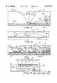
- FIG. 1depicts an example of the basic embodiment of the present invention, in which the holographic planar concentrator 10 is shown comprising highly transparent plate 12 and holographic film 14.
- the holographic film 14is mounted on the side 12a of the highly transparent plate 12 opposite that side 12b on which solar energy is incident.
- Careful selection of the refractive indices of the highly transparent plate and the holographic filmcan allow for coupling of light into the highly transparent plate at very steep angles as is shown in FIG. 1.
- the lightrepresented by rays 16, 16', 16" is seen as entering at an angle ⁇ in and being coupled into the highly transparent plate 12 at an angle ⁇ out as rays 18, 18' 18", respectively.
- the particular diffraction grating recorded, described in greater detail below, in the holographic film 14controls the angle ⁇ out .
- a wide acceptance angle ⁇ incan be coupled into the highly transparent plate 12 as a smaller angle ⁇ out .
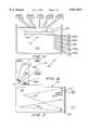
- the trapping anglesare not limited to small angles but rather a combination of angles are used in a spatially multiplexed approach, as is shown in FIG. 3.
- small trapping anglerefers to an angle of less than about 5 degrees.
- the holographic filmcomprises a plurality of regions, denoted 14, 114, 214, incident on each of which are rays 16, 16', 16", as described above.
- Each region 14, 114, 214has a different diffraction grating, resulting in a set of angles ⁇ out of light coupled into the highly transparent plate 12 that can either be identical to each other or different; however, the angle that the middle ray 18', 118', 218' of the set makes to the plane defined by the holographic film 14 is different in each case.
- This spatial multiplexing techniqueallows for multiple reflections from the holographic structure and hence larger trapping angles can be used.
- This approachreduces the need for a close index match between the highly transparent plate and the holographic film.
- a very good match between the refractive indexdiffers by only 0.01% but for a spatial multiplexed case, the refractive index may vary by up to 3.0% for a worst match scenario.
- Spatially multiplexing the multiplexed holographic optical structurecan produce HPC devices with functionally longer optical path lengths, thus increasing the functional size of the HPC panels and increasing the number of applications that the HPC can be used for.
- Spatially multiplexing the HPC holographic structurewill also avoid the limiting factor of beam degeneracy when angularly multiplexing and concentrating the gathered light. Beam degeneracy can also be avoided by utilizing the HPC device in a line focusing mode instead of a point focusing mode.
- Material dispersion effects of the mismatch between the refractive indices of the holographic film and the highly transparent platecan be minimized by designing the HPC device to perform at a wavelength where the refractive index of the glass matches that of the holographic film.
- the differing normal material dispersionwill then cause a divergence of the refractive indices of the glass and the film at other wavelengths differing from the design wavelength.
- the effect of dispersion on the overall match of the refractive indices between the film and the glassis that the index match really represents an average match over the chosen spectral range.
- the HPC of the present inventionis fabricated by attaching a holographic film or films to one side of an optical highly transparent plate.
- the holographic filmis attached to the side opposite of the incoming light.
- Recording of the master MHOSis performed in an index matched environment; these techniques are known by those skilled in this art.
- index matched environmentis meant that an appropriate material which is very transparent at the recording laser wavelength and matched in refractive index to the film is used in such a geometry to allow propagation of the laser beam into the film at very steep angles.
- index matchingThere have been many ways to bring laser beams into materials at steep angles and all require index matching. Different techniques utilize glass blocks, prisms and fluids in tanks.
- This techniqueis required for making the master hologram, but once the master is made, it only requires index matching the film to be copied to the master plate.
- the replicationalso requires that the recording be done in an index matched environment between master and copy, but it is a simpler process for mass production.
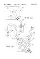
- One embodimentcan use a liquid gate or a tank filled with index matching fluid in which the hologram and attached highly transparent plate are placed for exposure, as illustrated in FIG. 4.
- the refractive index matching fluid in the tankshould be within about 12% of the refractive index of the holographic film and the highly transparent plate.
- a liquid with a refractive index slightly larger than the film and the highly transparent plateis employed. The better the match between the liquid and the highly transparent plate/film, the fewer noise gratings will be formed.
- FIG. 4shows the HPC 10 comprising the highly transparent plate 12 and holographic film 14 immersed in a tank 20 filled with a fluid 22 having substantially the same refractive index as the highly transparent plate 12.
- Object beams 22a-22eare incident on the top surface 12b of the highly transparent plate 12, while reference beams 24a-24e are incident on the exposed surface 14a of the holographic film 14.
- the lettersrepresent recording pair designation.
- the object beams 22a-22e and the reference beams 24a-24eare generated by techniques well-known in the art of holographic recording and do not form a part of this invention.
- the index matching tankprovides an environment which reduces the amount of stray light scattered from interfaces and other surfaces. This enhances the quality of the MHOS by minimizing the amount of optical noise in the recording process.
- Multiple laser beamsare used to record a unique holographic structure which will accept light from a range of input angles and direct the light down the optical highly transparent plate. Once in the optical highly transparent plate, the light is trapped so long as the light does not encounter any subsequent interactions with the same holographic structure.
- the recording processis a combination of angular, spectral and spatial multiplexing and can be performed in many ways by those skilled in the art.
- Each pair of recording wavefrontshas one object beam which mimics one narrow range of sun angles during the day and one reference beam which mimics the desired playback (concentrated) wavefront.
- the recording geometrysince the desired playback location varies for a given application or position.
- the HPChas the advantage of being recorded for different input angular ranges and different spectral collection requirements.
- the HPCcan be mounted vertically or tilted to the desired latitude of placement.
- the range of input anglesmay be chosen to be very narrow or very large, depending on the type of illumination available and the desired output spectrum.
- the beam recording geometriesvary with the grating design.
- the input angle range for, say, one multiplexed film recorded at 676 nm and 514 nm laser wavelengthswill be plus or minus 35 degrees from the normal in the medium and 100 to 140 degrees from the normal in the medium.
- Beam pairsare selected from this range of angles for producing the desired holographic structure to capture and concentrate the desired solar energy for the given location and mounting orientation.
- One preferred embodimentuses two recording pairs with angles of 30 and 100 degrees for one pair and -30 and 130 degrees for another pair.
- the HPCcan be used in either passive or active tracking modes, the use of angular multiplexing permits the use of passive tracking, which simplifies the overall structure and reduces cost.
- the HPC photovoltaic panelis mounted tilted to the latitude of installation and has the center angle of acceptance normal to the HPC front surface.
- the angular recordingthen mimics a variation of as much as approximately 160 degrees in the daily sun angle and 45 degrees in the seasonal sun angle. This represents a multitude of recording pairs, each launching their object beams at approximately 10 degree intervals.
- the hologram that is recordedincludes angular and spectral multiplexing.
- Spatial multiplexingis achieved by defining different regions in the holographic film, as described in greater detail below, and using the process depicted in FIG. 5 to record the angular and spectral multiplexing in each region.
- Light coupled into the highly transparent plate 12 in one spatial regionthus does not interact with the holographic film 14 in another spatial region.
- the use of the combination of regionsessentially avoids recoupling losses resulting from multiple interactions of the holographic film by the light confined in the highly transparent plate. This spatial multiplexing approach results in higher efficiency and the ability to create larger HPC devices.
- the MHOScan be recorded with gaussian or nongaussian beam profiles.
- the use of different beam profilesallow for control of the exposure intensity across the holographic film. This translates into control over the diffraction efficiency of the final MHOS.
- Intensity of the laser energy across the holographic filmis important in controlling the playback efficiency of the MHOS, since the quality of the holographic recording is determined in part by the intensity of the exposure energy striking the holographic film.
- the intensity of the recording energy across the filmshould be substantially uniform, by which is meant a variation in intensity of not more than about ⁇ 10 percent. Different holographic film materials require different exposure conditions and are more sensitive to exposure intensity.
- the uniformity of not more than about ⁇ 10 percentis a guideline to successfully fabricating HPC devices and is not necessarily the ideal exposure uniformity for every type of holographic film material.
- the HPC 10can also be fabricated using more than one layer of holographic film. By utilizing diffractive holographic structures, multiple layers can be used. Essentially, blue photons only interact with the MHOS sensitized to the blue portion of the solar spectrum and the red photons only interact with the film sensitized to the red part of the solar spectrum.
- Holographic reflective structureshave the ability to be fabricated in a range of spectral performance from very narrow (a few nanometers) to very broad (several hundred nanometers). This allows for the tailoring of the reflective holographic film with a spectral bandwidth of chosen size within these bounds.
- the HPC of the present inventionuses angular multiplexing to achieve a multitude of reflection type volume phase holograms in a single film. Many techniques exist for angularly multiplexing and are known to those skilled in the art.
- the preferred embodimentutilizes collimated and diverging recording wavefronts, although converging wavefronts may also be used.
- the wavefrontsare directed from opposite sides of the holographic film to produce a reflection-type volume phase holographic structure, as shown in FIGS. 4 and 5.
- the polarization of the wavefrontscan be chosen to achieve a maximum fringe contrast.
- the MHOScan be created utilizing several different wavelengths of laser light or a single wavelength with the recording angles adjusted to play back at the desired wavelengths.
- Single wavelength recordingcan be used to simulate multispectral recording by adjusting recording angles of the multiplexed reference and object beams such that a recording beam at one angle is designed to playback at a different angle and different wavelength. This is due to the relationship between angle and wavelength in diffractive structures.
- more than one holographic filmcan be used if required and applied over the first holographic film. The additional films can be used for increasing angular performance or broadening the spectral bandwidth of the HPC.
- Angularly multiplexing a single wavelengthcan result in an angular performance at the recording wavelength but also at other wavelengths with a different angular performance.
- the net effectis a single wavelength recording with enhanced spectral characteristics.
- the spectral sensitivity of the MHOScan be enhanced using techniques known in the art.
- the holographic structurecan be recorded with multiple laser wavelengths as well as multiple angular inputs. Recording with multiple wavelengths has the advantage of increasing the spectral sensitivity of the MHOS. In addition to recording with multiple wavelengths, it is also possible to nonlinearly shrink or swell the MHOS; this results in a series of fringes with varying spacing. The fringes with varying spacing has the effect of increasing the spectral bandwidth width of the HPC device.
- Each region of the MHOShas multiple gratings and a range of grating vectors.
- the different regionshave grating vector ranges that differ substantially so that the light confined in the highly transparent plate is not recoupled out of the HPC when it strikes regions of the MHOS on its way to the edge 12' of the highly transparent plate 12, as shown in FIG. 6, which is a top plan view.
- FIG. 6shows an example of a spatially multiplexed HPC 10, with each region 26a-26d with different grating vectors, resulting in coupled light 18a-18d incident on the edge 12' at different angles.
- the MHOSis divided into many different regions, with the regions in front of the advancing light having a different Bragg angle than the light striking that region as shown in FIG. 3. This technique prevents recoupling losses, since the subsequent reflections from the MHOS for light that is confined to the highly transparent plate strikes a holographic structure which has a substantially different grating vector than the spatial region from which the light was initially diffracted.
- the combination of the highly transparent plate 12 and the holographic film 14 regionsphysically form the total light trapping structure 10.
- the reason that the spatial multiplexing is required in the MHOSis because the light 18 has to pass through the holographic film 14 and bounce off the air/film interface to continue to be confined in the structure 10 by TIR.
- the light 18is required to remain in the total structure 10 in order to be delivered to the receiver 30, 32.
- the close refractive index match required to launch the light 16 into the glass or polymer highly transparent plate 12ensures that the light bounces back through the film 14 to the film/air interface.
- the present inventionrequires a fairly large area and hence long pathlengths to be a good solar collector. This is discussed above with regard to the particular example in connection with FIG.
- the HPCcan be designed to concentrate light in two dimensions, essentially a line focus (FIG. 7) or in three dimensions, essentially a point focus (FIGS. 8 and 9).
- the coupled rays 18are incident on a photovoltaic cell 30 mounted along the edge 12' of the highly transparent plate 12.
- the coupled rays 18are focused onto a light-receiving device, such as the photovoltaic cell 30 (FIG. 8) or a fiber optic lightguide 32 (FIG. 9).
- the HPC of the present inventionthe ability to create a focal region which is a square or rectangular region of any size, depending on the thickness of the highly transparent plate and the amount of focusing incorporated into the holographic structure.
- the focusingcan be accomplished with imaging or nonimaging techniques.
- the nonimaging techniqueproduces a square or rectangular region due to the subsequent internal reflections in the highly transparent plate.
- the imaging techniquecan be used to produce focal regions of varying shapes such as circular or elliptical focal regions.
- the two techniquescan also be combined to produce focal regions with the combined geometric properties of nonimaging and imaging focal regions.
- the intensity distribution in the focal planecan be adjusted using either the imaging or nonimaging recording techniques. This allows for more design freedom in the utilization of the concentrated light.
- One embodimentutilizes the spatial multiplexing approach combined with collimated recording beams to produce a tiled holographic structure of regions 26 the same size as the focal region 12' (FIG. 10).
- the collimated playback beams 18 from each tile 26 of the holographic structuresum at the focal region 12' to produce a concentration of the incoming light.
- This techniqueallows for the design of HPC devices that can avoid recoupling losses by designing the layout of the holographic regions such that the location and grating vector of the region avoids the recoupling of light out of the waveguide 12.
- the lines 34 normal to the light propagation vector 18represent a flat collimated wavefront.
- the holographic planar concentrator of the present inventionfunctions like a conventional two-stage concentrator that has been folded into the plane of the collecting device.
- Incoming light from a range of acceptance anglespasses through the optical highly transparent plate and is reflected/diffracted by the multiplexed holographic structure trapping the light in the plate and guiding it to one edge of the plate or to a focal region on the edge of the plate.
- larger plates with several HPC holographic structurescan be produced with multiple focal regions on different sides of the plate or focused into the corners of the plate. This basic scheme of operation can be used as the fundamental building block for many applications.
- the HPC of the present inventionbecomes an energy generating or energy redirecting product (FIGS. 7-9).
- the HPC deviceutilizes a multiplexed holographic structure along with the TIR trapping of the highly transparent plate.
- This two-stage concentrator approachworks similarly to some nonimaging optic concentrators which rely on TIR confinement of light. It is the combination of the unique multiplexed holographic structure and the TIR confinement which combine into the novel light concentrator of the present invention.
- the HPChas many advantages in terms of ease of fabrication and low material cost.
- the HPCcan be used to collect either direct light from the sun or diffuse light, such as light on cloudy days or light reflected from the surrounding environment.
- the HPCis intended to collect substantially all of the solar spectrum, particularly in the range of about 350 to 1400 nm.
- the four primary applications for the HPC productsare (1) solar electric power generation, (2) daylighting with natural sunlight, (3) thermal heating, and (4) windows which combine any or all of the three previous applications along with, optionally, the filtering of ultraviolet and infrared energy from sunlight.
- the four primary applicationare described below.
- the first deviceutilizes a photovoltaic cell to convert the concentrated light to electricity.
- FIGS. 7 and 8depict this embodiment. Any number of different photovoltaic conversion devices can be used and the output spectrum of the HPC can be engineered to more closely matched the bandgap of the conversion device to reduce the cooling required on the photovoltaic cell.
- the HPC photovoltaic (PV) panelutilizes the HPC with a PV cell to convert the light gathered by the HPC into electricity.
- the PV cellis directly bonded to the edge of the highly transparent plate, as shown in FIG. 7, creating an integrated PV panel.
- One embodiment(FIG. 7) has the entire edge 12' of the HPC 10 covered with one or more PV cells 30.
- Other embodimentsutilize a point focus HPC device 10 and a PV cell 30 mounted on the corner or side 12' of the highly transparent plate 12, such as shown in FIG. 8).
- the advantages of the HPC-PV panelinclude the following:
- Transparent HPCallows for additional films or collection devices behind the PV panel, hence minimizing costs associated with structural requirements and land requirements.
- a fiber optic cable 32is bonded to the edge of the HPC at the focal point of the concentrated light, as shown in FIG. 9.
- the light 18is launched directly into the fiber optic lightguide 32.
- Other embodimentscan include additional optics to improve the coupling efficiency between the HPC and the lightguide.
- the advantages of the HPC-skylightinclude:
- FIG. 11shows the fiber optic lightguide 32 secured to the edge 12' of the highly transparent plate 12.
- Solar energy 18is thus guided into a conventional hot water tank 36 filled with water 38.
- the solar spectrumis confined and absorbed within the hot water tank, thereby either heating the water directly (wavelengths absorbed by water molecules) or indirectly (wavelengths absorbed by hot water tank liner and re-radiated into the water).
- the advantages of the HPC-hot water heaterinclude:
- FIG. 12depicts one embodiment of the HPC window 10, with several edges, denoted here as 12', 112', and 212'.
- a photovoltaic cell 30is attached to edge 12', and, if it is a silicon PV cell, absorbs radiation in the region of about 700 to 1100 nm.
- a first fiber optic lightguide 32 attached to edge 112'is used to guide visible light (in the region of about 400 to 700 nm) into the interior of a building (not shown) to the side of which the window 10 is attached, to provide a natural source of light.
- a second fiber optic lightguide 132attached to edge 212', is used to guide primarily infrared energy in the region of about 700 to 1400 nm to a hot water tank 36 for heating the water 38 therein.
- Ultraviolet light(not shown) in the region of about 350 to 400 nm incident on the front surface 12b of the window 10 is blocked from passing through the window by the particular structure of the holographic film 14 (not shown in FIG. 12), attached to the back surface of the window; a suitable holographic grating and/or a UV-blocking component in the holographic film could be used, for example.
- HPC window 10 shown in FIG. 12is merely exemplary, and it will be appreciated by those skilled in this art that other devices and other combinations thereof may be employed to utilize various portions of the solar spectrum and/or block undesired portions thereof from passing through the window 10.
- the advantages of the HPC-windowinclude:
- FIG. 13depicts a building 38 employing a plurality of HPC windows 10, used with one or more of the devices described above.
- skylights 40 or separate solar panels 42comprising the HPC window 10, either roof-mounted or, in the case of solar panels, ground-supported, may be utilized.
- the solar panels 42may use either totally passive tracking or active tracking mechanisms, which are well-known in the art and thus not shown here.
- the HPC windows 10may be employed on the east, south, and west sides of the building 38 for collection of both direct and indirect solar radiation and on the north side of the building (in the northern hemisphere) or on the south side of the building (in the southern hemisphere) for collection of indirect solar radiation.
- Devicescomprising a multiplexed (angular and spectral) holographic film bonded to a glass plate have been fabricated with large angular acceptance.
- One experimentutilized three angular and three spectral multiplexed beams with a calculated light gathering efficiency of 20 percent.
- the angular performance of the deviceswas 160 degrees in the daily solar angular variation and 45 degrees in the seasonal angular variation.
- spatially-multiplexed deviceswere made that utilized different holographic structures to reduce recoupling losses.
- the devicesconcentrated light to one edge of the glass plate.
- the spatially-multiplexed holographic structurevaried from the region of the plate farthest from the edge that the light was concentrated to the region of the plate adjacent the edge that the light was concentrated to.
- the largest device constructed to dateis a 12 by 8.5 inch highly transparent acrylic plate, 6 mm thick with an active area of 8 by 8 inches (64 square inches). It utilized 3 layers of DuPont holographic film each layer representing a different spectral range (spectral multiplexing). The films were adhered with Norland NOA 65 optical adhesive. Each layer of holographic film had 44 different spatially multiplexed regions and each film was recorded using four multiplexed angular beams. Each spatial region was 50 mm by 15 mm. The regions varied from the output edge of the device linearly to the opposite edge of the HPC. The device showed a total solar collection efficiency of 2 percent at the optimum angle and calculated efficiency of 20 percent in the narrow wavelength band that it was recorded in 490 to 530 nanometers. It was constructed as a line focus HPC device.
- Another example of a preferred embodimentutilized a piece of 4 ⁇ 12 inch, 6 mm thick, low iron Solarphire glass with 2 layers of Dupont Omnidex holographic film adhered to the glass with Norland NOA 65 optical adhesive.
- the two layers of holographic filmwere multiplexed a total of 6 regions. These regions were angularly, spectrally, and spatially multiplexed.
- One filmcontained regions spatially multiplexed recorded at 500 nm, 568 nm, and 676 nm all with fringe angles of 37 degrees.
- the second film layercontained regions recorded at 500 nm, 568 nm, and 676 nm with a fringe angle of 40 degrees. This device performed with a collection efficiency of 13% total solar and 90% efficient in the desired collection bandwidth.
Landscapes
- Chemical & Material Sciences (AREA)
- Engineering & Computer Science (AREA)
- Physics & Mathematics (AREA)
- Organic Chemistry (AREA)
- Mechanical Engineering (AREA)
- Life Sciences & Earth Sciences (AREA)
- Sustainable Energy (AREA)
- Combustion & Propulsion (AREA)
- Sustainable Development (AREA)
- General Engineering & Computer Science (AREA)
- Thermal Sciences (AREA)
- Chemical Kinetics & Catalysis (AREA)
- General Physics & Mathematics (AREA)
- Optics & Photonics (AREA)
- Diffracting Gratings Or Hologram Optical Elements (AREA)
- Optical Couplings Of Light Guides (AREA)
- Holo Graphy (AREA)
- Photovoltaic Devices (AREA)
Abstract
Description
Claims (44)
Priority Applications (11)
| Application Number | Priority Date | Filing Date | Title |
|---|---|---|---|
| US08/897,068US5877874A (en) | 1995-08-24 | 1997-07-18 | Device for concentrating optical radiation |
| CA002294908ACA2294908A1 (en) | 1997-07-18 | 1998-07-16 | Device for concentrating optical radiation |
| AU84927/98AAU722844B2 (en) | 1997-07-18 | 1998-07-16 | Device for concentrating optical radiation |
| JP2000503454AJP2001510902A (en) | 1997-07-18 | 1998-07-16 | Light radiation focusing device |
| CN98807177ACN1263603A (en) | 1997-07-18 | 1998-07-16 | Device for concentrating optical radiation |
| PCT/US1998/014774WO1999004296A1 (en) | 1997-07-18 | 1998-07-16 | Device for concentrating optical radiation |
| BR9811924-9ABR9811924A (en) | 1997-07-18 | 1998-07-16 | Optical radiation concentration device |
| IL13375798AIL133757A0 (en) | 1997-07-18 | 1998-07-16 | Device for concentrating optical radiation |
| KR1020007000573AKR20010022006A (en) | 1997-07-18 | 1998-07-16 | Device for concentrating optical radiation |
| TW087111606ATW369610B (en) | 1997-07-18 | 1998-07-16 | Device for concentrating optical radiation |
| EP98935743AEP1023619A1 (en) | 1997-07-18 | 1998-07-16 | Device for concentrating optical radiation |
Applications Claiming Priority (2)
| Application Number | Priority Date | Filing Date | Title |
|---|---|---|---|
| US51876095A | 1995-08-24 | 1995-08-24 | |
| US08/897,068US5877874A (en) | 1995-08-24 | 1997-07-18 | Device for concentrating optical radiation |
Related Parent Applications (1)
| Application Number | Title | Priority Date | Filing Date |
|---|---|---|---|
| US51876095AContinuation-In-Part | 1995-08-24 | 1995-08-24 |
Publications (1)
| Publication Number | Publication Date |
|---|---|
| US5877874Atrue US5877874A (en) | 1999-03-02 |
Family
ID=25407295
Family Applications (1)
| Application Number | Title | Priority Date | Filing Date |
|---|---|---|---|
| US08/897,068Expired - LifetimeUS5877874A (en) | 1995-08-24 | 1997-07-18 | Device for concentrating optical radiation |
Country Status (11)
| Country | Link |
|---|---|
| US (1) | US5877874A (en) |
| EP (1) | EP1023619A1 (en) |
| JP (1) | JP2001510902A (en) |
| KR (1) | KR20010022006A (en) |
| CN (1) | CN1263603A (en) |
| AU (1) | AU722844B2 (en) |
| BR (1) | BR9811924A (en) |
| CA (1) | CA2294908A1 (en) |
| IL (1) | IL133757A0 (en) |
| TW (1) | TW369610B (en) |
| WO (1) | WO1999004296A1 (en) |
Cited By (156)
| Publication number | Priority date | Publication date | Assignee | Title |
|---|---|---|---|---|
| WO2000074147A1 (en)* | 1999-05-28 | 2000-12-07 | Terrasun, Llc | Device for concentrating optical radiation |
| US6407832B1 (en) | 1999-11-19 | 2002-06-18 | Zebra Imaging, Inc. | Light source following optical system for hologram illumination |
| WO2002050590A1 (en) | 2000-12-21 | 2002-06-27 | Led Products, Inc. | Light conduit with radial light ejecting structure |
| US6425391B1 (en) | 2001-05-23 | 2002-07-30 | Jeffrey A. Davoren | Electromagnetic radiation collector system |
| US20020159109A1 (en)* | 1998-04-15 | 2002-10-31 | Duke University | Projection screen apparatus including holographic optical element |
| WO2002101428A1 (en)* | 2001-06-11 | 2002-12-19 | Aprilis, Inc. | Holographic filter with a wide angular field of view and a narrow spectral bandwidth |
| US20030154973A1 (en)* | 2002-02-15 | 2003-08-21 | Biosynergetics, Inc. | Electromagnetic radiation collector and transport system |
| US20030206342A1 (en)* | 1993-05-12 | 2003-11-06 | Bright View Technologies, Inc. | Micro-lens array based light transmission screen |
| US20030210462A1 (en)* | 1998-04-15 | 2003-11-13 | Bright View Technologies, Inc. | Micro-lens array based light transmitting screen with tunable gain |
| US20040008411A1 (en)* | 1998-04-15 | 2004-01-15 | Bright View Technologies, Inc. | Micro-lens array based light transmitting screen with high resolution and low imaging artifacts |
| US20040017612A1 (en)* | 1998-04-15 | 2004-01-29 | Bright View Technologies, Inc. | Micro-lens array with precisely aligned aperture mask and methods of producing same |
| US20040123895A1 (en)* | 2002-10-22 | 2004-07-01 | Sunray Technologies, Inc. | Diffractive structures for the redirection and concentration of optical radiation |
| US6775958B2 (en)* | 2000-03-10 | 2004-08-17 | Seiko Epson Corporation | Package sealing method, manufacturing method of electronic device modules, sealing apparatus, and packaged product |
| US6788460B2 (en) | 1998-04-15 | 2004-09-07 | Duke University | Projection screen apparatus |
| US20050213233A1 (en)* | 2002-06-18 | 2005-09-29 | Photosolar Aps C/O Teknologisk Institut | Optical element for shielding against light |
| US20050279400A1 (en)* | 2002-08-16 | 2005-12-22 | Mark Banister | Electric tile modules |
| US20060077522A1 (en)* | 2004-09-27 | 2006-04-13 | Manish Kothari | Method and device for compensating for color shift as a function of angle of view |
| US20060077514A1 (en)* | 2004-09-27 | 2006-04-13 | Sampsell Jeffrey B | System and method of reducing color shift in a display |
| US20060137734A1 (en)* | 2002-11-20 | 2006-06-29 | Mortenson Mark G | High efficiency solar cells |
| US7078612B1 (en) | 2005-12-31 | 2006-07-18 | Edward Ronwin | Photon battery |
| US20060235717A1 (en)* | 2005-04-18 | 2006-10-19 | Solaria Corporation | Method and system for manufacturing solar panels using an integrated solar cell using a plurality of photovoltaic regions |
| US20060274400A1 (en)* | 1995-11-06 | 2006-12-07 | Miles Mark W | Method and device for modulating light with optical compensation |
| US20060283495A1 (en)* | 2005-06-06 | 2006-12-21 | Solaria Corporation | Method and system for integrated solar cell using a plurality of photovoltaic regions |
| US20070047932A1 (en)* | 2005-08-31 | 2007-03-01 | Branson Ultrasonics Corporation | Waveguide for plastics welding using an incoherent infrared light source |
| US20070171418A1 (en)* | 2002-02-15 | 2007-07-26 | Nyhart Eldon H Jr | Communication Terminal Apparatus And Wireless Transmission Method |
| US20070251571A1 (en)* | 2006-04-26 | 2007-11-01 | Jacobs Gregory F | Shingle with photovoltaic element(s) and array of same laid up on a roof |
| USD555084S1 (en) | 2005-11-18 | 2007-11-13 | Solaria Corporation | Circular solar cell package design |
| USD555083S1 (en) | 2005-11-08 | 2007-11-13 | Solaria Corporation | Solar cell package design |
| USD558139S1 (en) | 2005-11-18 | 2007-12-25 | Solaria Corporation | Triangular solar cell design |
| USD559174S1 (en) | 2005-11-18 | 2008-01-08 | Solaria Corporation | Shaped solar cell package design |
| US20080006323A1 (en)* | 2006-07-08 | 2008-01-10 | Kalkanoglu Husnu M | Photovoltaic Module |
| US20080011289A1 (en)* | 2006-07-14 | 2008-01-17 | National Science And Technology Development Agency | Photovoltaic thermal (PVT) collector |
| US20080029149A1 (en)* | 2006-08-02 | 2008-02-07 | Daniel Simon | Method and apparatus for arranging a solar cell and reflector |
| US20080073198A1 (en)* | 2006-08-03 | 2008-03-27 | Daniel Simon | Concentrating solar distillation apparatus |
| USD568238S1 (en) | 2005-11-18 | 2008-05-06 | Solaria Corporation | Rectangular solar cell package design |
| US20080112039A1 (en)* | 2004-02-03 | 2008-05-15 | Idc, Llc | Spatial light modulator with integrated optical compensation structure |
| US7391939B1 (en) | 2004-11-17 | 2008-06-24 | Williams Raymond W | Optical apparatus |
| US20080178922A1 (en)* | 2005-07-26 | 2008-07-31 | Solaria Corporation | Method and system for manufacturing solar panels using an integrated solar cell using a plurality of photovoltaic regions |
| US20080185033A1 (en)* | 2007-02-06 | 2008-08-07 | Kalejs Juris P | Solar electric module |
| US20080192259A1 (en)* | 2007-02-09 | 2008-08-14 | Seiko Epson Corporation | Volume hologram, light source device, illumination device, monitor, and image display device |
| US20080236651A1 (en)* | 2007-04-02 | 2008-10-02 | Solaria Corporation | Solar cell concentrator structure including a plurality of concentrator elements with a notch design and method having a predetermined efficiency |
| US20080236655A1 (en)* | 2007-03-29 | 2008-10-02 | Baldwin Daniel F | Solar module manufacturing processes |
| US20080236664A1 (en)* | 2007-04-02 | 2008-10-02 | Solaria Corporation | Method and system for assembling a solar cell package |
| FR2914754A1 (en)* | 2007-04-05 | 2008-10-10 | Commissariat Energie Atomique | PLAN LIGHT CONCENTRATION DEVICE WITH REDUCED THICKNESS |
| US20080257400A1 (en)* | 2007-04-17 | 2008-10-23 | Mignon George V | Holographically enhanced photovoltaic (hepv) solar module |
| US20080271776A1 (en)* | 2007-05-01 | 2008-11-06 | Morgan Solar Inc. | Light-guide solar panel and method of fabrication thereof |
| US20080289689A1 (en)* | 2007-05-21 | 2008-11-27 | Solaria Corporation | Concentrating module and method of manufacture for photovoltaic strips |
| US20090027872A1 (en)* | 2005-02-16 | 2009-01-29 | Stichting Voor De Technische Wetenschappen | Luminescent object comprising aligned polymers having a specific pretilt angle |
| US20090032087A1 (en)* | 2007-02-06 | 2009-02-05 | Kalejs Juris P | Manufacturing processes for light concentrating solar module |
| US20090056788A1 (en)* | 2007-09-05 | 2009-03-05 | Solaria Corporation | Notch structure for concentrating module and method of manufacture using photovoltaic strips |
| US20090067784A1 (en)* | 2007-09-10 | 2009-03-12 | Banyan Energy, Inc. | Compact optics for concentration, aggregation and illumination of light energy |
| US20090064993A1 (en)* | 2007-09-10 | 2009-03-12 | Banyan Energy, Inc. | Solar energy concentrator |
| USD588534S1 (en) | 2007-07-26 | 2009-03-17 | Solaria Corporation | Shaped solar cell package |
| USD591229S1 (en) | 2008-01-24 | 2009-04-28 | Solaria Corporation | Shaped solar cell package |
| US20090120487A1 (en)* | 2005-09-12 | 2009-05-14 | Solaria Corporation | Method and System for Assembling A Solar Cell Using a Plurality of Photovoltaic Regions |
| US20090126792A1 (en)* | 2007-11-16 | 2009-05-21 | Qualcomm Incorporated | Thin film solar concentrator/collector |
| US20090152745A1 (en)* | 2007-12-12 | 2009-06-18 | Solaria Corporation | Method and system for manufacturing integrated molded concentrator photovoltaic device |
| US20090151770A1 (en)* | 2007-12-12 | 2009-06-18 | Solaria Corporation | Method and material for coupling solar concentrators and photovoltaic devices |
| US20090178704A1 (en)* | 2007-02-06 | 2009-07-16 | Kalejs Juris P | Solar electric module with redirection of incident light |
| US20090185302A1 (en)* | 2007-11-08 | 2009-07-23 | Sunrgi | Light concentrator structures and methods |
| US20090188563A1 (en)* | 2007-09-05 | 2009-07-30 | Solaria Corporation | Solar Cell Structure Including A Plurality of Concentrator Elements With A Notch Design and Predetermined Radii and Method |
| US20090194096A1 (en)* | 2008-02-05 | 2009-08-06 | Daniel Simon | Method and apparatus for concentrating optical radiation using light trapping elements |
| US20090194165A1 (en)* | 2008-01-31 | 2009-08-06 | Primestar Solar, Inc. | Ultra-high current density cadmium telluride photovoltaic modules |
| US20090194146A1 (en)* | 2008-02-06 | 2009-08-06 | Daniel Simon | Method and apparatus for arranging multiple flat reflector facets around a solar cell or solar panel |
| US20090242021A1 (en)* | 2008-03-31 | 2009-10-01 | Noribachi Llc | Solar cell with colorization layer |
| US20090301469A1 (en)* | 2006-07-28 | 2009-12-10 | Angus Muir Edington Scrimgeour | Solar collectors |
| US20090316361A1 (en)* | 2008-06-23 | 2009-12-24 | Daniel Simon | Method and apparatus for controlling the output of solar arrays |
| US20100051089A1 (en)* | 2008-09-02 | 2010-03-04 | Qualcomm Mems Technologies, Inc. | Light collection device with prismatic light turning features |
| WO2008141621A3 (en)* | 2007-05-21 | 2010-04-08 | Solartec Ag | Photovoltaic device comprising solar cells that are laterally mounted on optical elements |
| US20100103488A1 (en)* | 2006-10-10 | 2010-04-29 | Qualcomm Mems Technologies, Inc. | Display device with diffractive optics |
| US20100108056A1 (en)* | 2008-11-06 | 2010-05-06 | Industrial Technology Research Institute | Solar energy collecting module |
| US20100116336A1 (en)* | 2008-11-12 | 2010-05-13 | Abengoa Solar New Technologies, S.A. | Light Collection and Concentration System |
| US20100126555A1 (en)* | 2008-11-20 | 2010-05-27 | Hoozad Inc. | Concentrating photovoltaic photo-current balancing system |
| US20100133422A1 (en)* | 2008-12-03 | 2010-06-03 | Industrial Technology Research Institute | Light concentrating module |
| US20100177387A1 (en)* | 2009-01-15 | 2010-07-15 | Microsoft Corporation | End reflector for a flat panel lens |
| US20100180946A1 (en)* | 2008-09-18 | 2010-07-22 | Qualcomm Mems Technologies, Inc. | Increasing the angular range of light collection in solar collectors/concentrators |
| US20100180937A1 (en)* | 2008-06-30 | 2010-07-22 | General Electric Company | Holographic energy-collecting medium and associated device |
| US7817885B1 (en) | 2009-06-24 | 2010-10-19 | University Of Rochester | Stepped light collection and concentration system, components thereof, and methods |
| US20100278480A1 (en)* | 2009-04-21 | 2010-11-04 | Vasylyev Sergiy V | Light collection and illumination systems employing planar waveguide |
| RU2403510C1 (en)* | 2009-07-06 | 2010-11-10 | Государственное Научное Учреждение "Институт Физики Имени Б.И. Степанова Национальной Академии Наук Беларуси" | Holographic solar concentrator |
| US20100282318A1 (en)* | 2008-01-08 | 2010-11-11 | Kalkanoglu Husnu M | Photovoltaic module |
| US20100282316A1 (en)* | 2007-04-02 | 2010-11-11 | Solaria Corporation | Solar Cell Concentrator Structure Including A Plurality of Glass Concentrator Elements With A Notch Design |
| US7845841B2 (en) | 2006-08-28 | 2010-12-07 | Qualcomm Mems Technologies, Inc. | Angle sweeping holographic illuminator |
| US20100307480A1 (en)* | 2006-07-28 | 2010-12-09 | Angus Muir Edington Scrimgeour | Non-tracking solar collectors |
| WO2010151253A1 (en)* | 2009-06-24 | 2010-12-29 | University Of Rochester | Dimpled light collection and concentration system, components thereof, and methods |
| ITMI20091225A1 (en)* | 2009-07-09 | 2011-01-10 | Raul Maria Orlandi | INTEGRATED SYSTEM WITH VERY HIGH VALUE OF ENERGY CONVERSION INCLUDING HOLOGRAPHIC, THERMAL AND ANY OPTICAL ELEMENTS TO TRANSFORM SOLAR ENERGY IN ECO-FRIENDLY ENERGY. |
| US20110011449A1 (en)* | 2007-05-01 | 2011-01-20 | Morgan Solar Inc. | Light-guide solar panel and method of fabrication thereof |
| US20110017199A1 (en)* | 2009-07-24 | 2011-01-27 | Jorge Simon Hernandez | Apparatus and Method for Collecting and Distributing Radiation |
| US20110017263A1 (en)* | 2007-09-05 | 2011-01-27 | Solaria Corporation | Method and device for fabricating a solar cell using an interface pattern for a packaged design |
| US20110030763A1 (en)* | 2009-08-07 | 2011-02-10 | Jeffrey Lewis | Solar Panel Apparatus Created By Laser Etched Gratings on Glass Substrate |
| DE102009032575A1 (en) | 2009-07-10 | 2011-02-17 | Carl Zeiss Ag | Optical arrangement for deflecting and concentrating sunlight on solar cell in solar power plant, has plate aligned to light source so that light is transmitted to Fresnel-structure and enters through boundary surface to medium i.e. air |
| WO2011024181A2 (en) | 2009-08-31 | 2011-03-03 | Bar Ilan University | Collector and concentrator of solar radiation |
| US7910822B1 (en) | 2005-10-17 | 2011-03-22 | Solaria Corporation | Fabrication process for photovoltaic cell |
| US20110132458A1 (en)* | 2009-12-09 | 2011-06-09 | Wen-Chun Wang | Solar light-control module |
| US20120147443A1 (en)* | 2010-12-08 | 2012-06-14 | Samsung Electronics Co., Ltd. | Solar light concentration plate |
| US8227688B1 (en) | 2005-10-17 | 2012-07-24 | Solaria Corporation | Method and resulting structure for assembling photovoltaic regions onto lead frame members for integration on concentrating elements for solar cells |
| US20120204937A1 (en)* | 2011-02-11 | 2012-08-16 | AMI Research & Development, LLC | Leaky solar array with spatially separated collectors |
| US8328403B1 (en) | 2012-03-21 | 2012-12-11 | Morgan Solar Inc. | Light guide illumination devices |
| US8412010B2 (en) | 2007-09-10 | 2013-04-02 | Banyan Energy, Inc. | Compact optics for concentration and illumination systems |
| US20130133744A1 (en)* | 2011-11-30 | 2013-05-30 | Michael Etienne | Optical Trapping For Fiber Illumination |
| US8513095B1 (en) | 2007-09-04 | 2013-08-20 | Solaria Corporation | Method and system for separating photovoltaic strips |
| TWI415282B (en)* | 2008-10-02 | 2013-11-11 | Atomic Energy Council | Method for making a silicon quantum dot planar concentrating solar cell |
| USD699176S1 (en) | 2011-06-02 | 2014-02-11 | Solaria Corporation | Fastener for solar modules |
| US20140041796A1 (en)* | 2010-08-09 | 2014-02-13 | Dexerials Corporation | Optical element, method of manufacturing optical element, illumination device, window member, and fitting |
| US8705914B2 (en) | 2007-09-10 | 2014-04-22 | Banyan Energy, Inc. | Redirecting optics for concentration and illumination systems |
| US8707736B2 (en) | 2007-08-06 | 2014-04-29 | Solaria Corporation | Method and apparatus for manufacturing solar concentrators using glass process |
| US20140130864A1 (en)* | 2012-11-09 | 2014-05-15 | Board Of Trustees Of Michigan State University | Transparent Luminescent Solar Concentrators For Integrated Solar Windows |
| US8798425B2 (en) | 2007-12-07 | 2014-08-05 | Qualcomm Mems Technologies, Inc. | Decoupled holographic film and diffuser |
| JP2014525050A (en)* | 2011-07-01 | 2014-09-25 | トロピグラス テクノロジーズ リミテッド | Spectral selectivity panel |
| US8872085B2 (en) | 2006-10-06 | 2014-10-28 | Qualcomm Mems Technologies, Inc. | Display device having front illuminator with turning features |
| US8885995B2 (en) | 2011-02-07 | 2014-11-11 | Morgan Solar Inc. | Light-guide solar energy concentrator |
| US8902484B2 (en) | 2010-12-15 | 2014-12-02 | Qualcomm Mems Technologies, Inc. | Holographic brightness enhancement film |
| US8928967B2 (en) | 1998-04-08 | 2015-01-06 | Qualcomm Mems Technologies, Inc. | Method and device for modulating light |
| US8934743B2 (en) | 2011-11-08 | 2015-01-13 | Panasonic Corporation | Light-receiving device having light-trapping sheet |
| ES2527969A1 (en)* | 2013-08-01 | 2015-02-02 | Instituto Holográfico Andaluz, S.L. | Three-dimensional thermal or photovoltaic solar panel with integral holograph |
| US8971675B2 (en) | 2006-01-13 | 2015-03-03 | Qualcomm Mems Technologies, Inc. | Interconnect structure for MEMS device |
| US9019183B2 (en) | 2006-10-06 | 2015-04-28 | Qualcomm Mems Technologies, Inc. | Optical loss structure integrated in an illumination apparatus |
| US9025235B2 (en) | 2002-12-25 | 2015-05-05 | Qualcomm Mems Technologies, Inc. | Optical interference type of color display having optical diffusion layer between substrate and electrode |
| US9036963B2 (en) | 2009-06-24 | 2015-05-19 | University Of Rochester | Light collecting and emitting apparatus, method, and applications |
| US9103978B2 (en) | 2011-11-08 | 2015-08-11 | Panasonic Intellectual Property Management Co., Ltd. | Light-trapping sheet, and light-receiving device and light-emitting device using the same |
| US9110289B2 (en) | 1998-04-08 | 2015-08-18 | Qualcomm Mems Technologies, Inc. | Device for modulating light with multiple electrodes |
| US9188717B2 (en) | 2010-10-04 | 2015-11-17 | Panasonic Intellectual Property Management Co., Ltd. | Light acquisition sheet and rod, and light receiving device and light emitting device each using the light acquisition sheet or rod |
| WO2016012813A2 (en) | 2014-07-24 | 2016-01-28 | Bowater Holographic Research Limited | Holographic windows |
| US20160041387A1 (en)* | 2013-03-28 | 2016-02-11 | Bae Systems Plc | Improvements in and relating to displays |
| US9281424B2 (en) | 2012-01-24 | 2016-03-08 | AMI Research & Development, LLC | Wideband light energy waveguide and detector |
| WO2016044462A1 (en) | 2014-09-16 | 2016-03-24 | Nitto Denko Corporation | Transparent composite for improved indoor illumination |
| WO2016044225A1 (en) | 2014-09-16 | 2016-03-24 | Nitto Denko Corporation | Highly transparent films comprising holographic optical elements useful for reducing solar heating |
| WO2016057561A1 (en) | 2014-10-06 | 2016-04-14 | Nitto Denko Corporation | Electronic device comprising a holographic solar concentrator integrated in its display |
| US9316786B2 (en) | 2011-11-08 | 2016-04-19 | Panasonic Intellectual Property Management Co., Ltd. | Light-trapping sheet and rod, and light-receiving device and light-emitting device using the same |
| US9337373B2 (en) | 2007-05-01 | 2016-05-10 | Morgan Solar Inc. | Light-guide solar module, method of fabrication thereof, and panel made therefrom |
| US20160276514A1 (en)* | 2013-11-12 | 2016-09-22 | Nitto Denko Corporation | Solar energy collection systems utilizing holographic optical elements useful for building integrated photovoltaics |
| WO2016168383A1 (en)* | 2015-04-14 | 2016-10-20 | Face International Corporation | Systems and methods for producing scattering selected wavelengths of electromagnetic energy |
| RU2608797C2 (en)* | 2014-12-10 | 2017-01-24 | Федеральное государственное бюджетное научное учреждение Федеральный научный агроинженерный центр ВИМ (ФГБНУ ФНАЦ ВИМ) | Solar module with concentrator (versions) |
| US9557480B2 (en) | 2013-11-06 | 2017-01-31 | R.A. Miller Industries, Inc. | Graphene coupled MIM rectifier especially for use in monolithic broadband infrared energy collector |
| US9893223B2 (en) | 2010-11-16 | 2018-02-13 | Suncore Photovoltaics, Inc. | Solar electricity generation system |
| US20180138346A1 (en)* | 2015-05-12 | 2018-05-17 | Nitto Denko Corporation | Solar Energy Collection Systems Utilizing Holographic Optical Elements Useful for Building Integrated Photovoltaics |
| US20190049739A1 (en)* | 2017-08-14 | 2019-02-14 | Samsung Electronics Co., Ltd. | Light guide plate, backlight unit, and holographic display apparatus including the backlight unit |
| US10247861B2 (en) | 2017-01-25 | 2019-04-02 | Face International Corporation | Compositions of materials for forming coatings and layered structures including elements for scattering and passing selectively tunable wavelengths of electromagnetic energy |
| US10546968B2 (en) | 2013-02-21 | 2020-01-28 | HolFocus, LLC | Solar concentration system using volume holograms |
| EP3535611A4 (en)* | 2016-11-03 | 2020-06-24 | Basf Se | Daylighting illumination system |
| CN111413764A (en)* | 2020-05-22 | 2020-07-14 | 宋建明 | Passive brightness enhancement method and waveguide grating passive brightness energy superposition enhancement device |
| US10795062B2 (en) | 2015-04-14 | 2020-10-06 | Face International Corporation | Systems and methods for producing objects incorporating selective electromagnetic energy scattering layers, laminates and coatings |
| US10879838B2 (en) | 2017-01-26 | 2020-12-29 | Face International Corporation | Security and tracking systems including energy harvesting components for providing autonomous electrical power |
| US10886423B2 (en) | 2017-01-26 | 2021-01-05 | Face International Corporation | Energy harvesting systems for providing autonomous electrical power to building structures and electrically-powered devices in the building structures |
| US10886873B2 (en) | 2017-01-26 | 2021-01-05 | Face International Corporation | Energy harvesting methods for providing autonomous electrical power to building structures and electrically-powered devices in the building structures |
| US10929640B2 (en) | 2017-09-07 | 2021-02-23 | Lg Display Co., Ltd. | Flat panel display with optical image sensor embedded therein |
| US11009632B2 (en) | 2017-01-25 | 2021-05-18 | Face International Corporation | Methods for making compositions of materials for forming coatings and layered structures including elements for scattering and passing selectively tunable wavelengths of electromagnetic energy |
| WO2021141939A1 (en)* | 2020-01-07 | 2021-07-15 | Tru-UV, LLC | Uv-c emitting fabric |
| US11310637B2 (en) | 2017-01-26 | 2022-04-19 | Face International Corporation | Methods for producing security and tracking systems including energy harvesting components for providing autonomous electrical power |
| US11554576B2 (en) | 2017-01-26 | 2023-01-17 | Face International Corporation | Energy harvesting methods for providing autonomous electrical power to mobile devices |
| US11569402B2 (en) | 2017-05-09 | 2023-01-31 | UbiQD, Inc. | Luminescent optical elements for agricultural applications |
| US11723274B2 (en) | 2010-09-20 | 2023-08-08 | Certainteed Llc | Solar thermoelectric power generation system, and process for making same |
| US11966066B2 (en) | 2017-01-25 | 2024-04-23 | Face International Corporation | Delivery systems and methods for compositions of materials for forming coatings and layered structures including elements for scattering and passing selectively tunable wavelengths of electromagnetic energy |
| EP4446820A1 (en)* | 2023-04-14 | 2024-10-16 | Singular Control Energy, SL | Holographic system and method for the optimisation of incident solar radiation |
| US12181693B2 (en) | 2015-04-14 | 2024-12-31 | Face International Corporation | Image capturing system with wavelength-selective energy scattering layer |
| US12247126B2 (en) | 2018-05-09 | 2025-03-11 | Board Of Trustees Of Michigan State University | Near-infrared harvesting transparent luminescent solar concentrators with engineered stokes shift |
Families Citing this family (19)
| Publication number | Priority date | Publication date | Assignee | Title |
|---|---|---|---|---|
| US7750886B2 (en) | 2004-09-27 | 2010-07-06 | Qualcomm Mems Technologies, Inc. | Methods and devices for lighting displays |
| DE102005018336A1 (en) | 2005-02-28 | 2006-08-31 | Osram Opto Semiconductors Gmbh | Optical fiber for use in optoelectronic component e.g. light emitting diode, has uneven light aperture, in which large portion of electromagnetic radiation generated by light source enters into fiber due to unevenness of aperture |
| US8507785B2 (en) | 2007-11-06 | 2013-08-13 | Pacific Integrated Energy, Inc. | Photo induced enhanced field electron emission collector |
| US8941631B2 (en) | 2007-11-16 | 2015-01-27 | Qualcomm Mems Technologies, Inc. | Simultaneous light collection and illumination on an active display |
| KR20100094511A (en)* | 2007-11-16 | 2010-08-26 | 퀄컴 엠이엠스 테크놀로지스, 인크. | Thin film planar sonar concentrator/ collector and diffusor used with an active display |
| CN101946334B (en)* | 2008-02-12 | 2013-08-21 | 高通Mems科技公司 | Dual layer thin film holographic solar concentrator/collector |
| FR2938078B1 (en)* | 2008-11-03 | 2011-02-11 | Saint Gobain | GLAZING WITH ZONES CONCENTRATING THE LIGHT BY IONIC EXCHANGE. |
| WO2010085286A1 (en) | 2009-01-23 | 2010-07-29 | Qualcomm Mems Technologies, Inc. | Integrated light emitting and light detecting device |
| WO2011156519A2 (en)* | 2010-06-08 | 2011-12-15 | Pacific Integrated Energy, Inc. | Optical antennas with enhanced fields and electron emission |
| CN103403592B (en)* | 2011-11-29 | 2016-10-19 | 松下知识产权经营株式会社 | Light-taking plate and rod, and light-receiving device and light-emitting device using them |
| US9599959B2 (en)* | 2012-09-10 | 2017-03-21 | Universite Libre De Bruxelles | Method for recording gabor hologram |
| HK1217816A1 (en)* | 2013-01-21 | 2017-01-20 | Holomedia Llc | Light-concentrating mechanism, photovoltaic power generation device, window structure, and window glass |
| JP2015231016A (en)* | 2014-06-06 | 2015-12-21 | Tdk株式会社 | solar battery |
| JP2016004809A (en)* | 2014-06-13 | 2016-01-12 | Tdk株式会社 | solar battery |
| ES2563645B1 (en)* | 2014-09-15 | 2016-12-29 | Instituto Holografico Terrasun,S.L. | Modular solar concentration system without tracking by combining conventional optics and holographic optical elements (HOE’s) |
| US10180520B2 (en) | 2015-08-24 | 2019-01-15 | Akonia Holographics, Llc | Skew mirrors, methods of use, and methods of manufacture |
| ITUA20162918A1 (en)* | 2016-04-27 | 2017-10-27 | Univ Degli Studi Di Milano Bicocca | LUMINESCENT SOLAR CONCENTRATOR WITH WIDE AREA OF INDIRECT GAP-BASED NANOCRYSTALS |
| DE102018209305A1 (en)* | 2018-06-12 | 2019-12-12 | Robert Bosch Gmbh | Foil for a touch-sensitive screen, screen with film, device, in particular mobile device, with screen and method for sensing a print intensity using a film |
| KR20210060848A (en) | 2019-11-19 | 2021-05-27 | 주식회사 미래기술연구소 | Holographic condensing film fixed to solar panel |
Citations (16)
| Publication number | Priority date | Publication date | Assignee | Title |
|---|---|---|---|---|
| US4012150A (en)* | 1975-08-18 | 1977-03-15 | Environmental Research Institute Of Michigan | Holographic light line sight |
| US4309070A (en)* | 1979-01-19 | 1982-01-05 | Smiths Industries Limited | Display apparatus |
| US4412528A (en)* | 1980-04-11 | 1983-11-01 | Exxon Research And Engineering Co. | Heat storage window |
| US4418238A (en)* | 1981-10-20 | 1983-11-29 | Lidorenko Nikolai S | Photoelectric solar cell array |
| US4490981A (en)* | 1982-09-29 | 1985-01-01 | Milton Meckler | Fixed solar concentrator-collector-satelite receiver and co-generator |
| US4505264A (en)* | 1983-12-27 | 1985-03-19 | Universite Laval | Electromagnetic wave concentrator |
| US4643515A (en)* | 1985-04-01 | 1987-02-17 | Environmental Research Institute Of Michigan | Method and apparatus for recording and displaying edge-illuminated holograms |
| US4682841A (en)* | 1981-06-15 | 1987-07-28 | Afian Viktor V | Light radiation concentrator and method of making the same |
| US4691994A (en)* | 1981-10-06 | 1987-09-08 | Afian Viktor V | Method for a solar concentrator manufacturing |
| US4711512A (en)* | 1985-07-12 | 1987-12-08 | Environmental Research Institute Of Michigan | Compact head-up display |
| US4863224A (en)* | 1981-10-06 | 1989-09-05 | Afian Viktor V | Solar concentrator and manufacturing method therefor |
| US5039352A (en)* | 1989-05-30 | 1991-08-13 | Mueller Helmut F O | External wall element for buildings |
| US5048925A (en)* | 1985-05-28 | 1991-09-17 | Advanced Environmental Research Group | Quasi volume diffracting structures |
| US5151800A (en)* | 1990-12-17 | 1992-09-29 | Environmental Research Institute Of Michigan | Compact hologram displays & method of making compact hologram |
| US5268985A (en)* | 1991-07-30 | 1993-12-07 | Nippondenso Co., Ltd. | Light-guiding device having a hologram layer |
| US5517339A (en)* | 1994-06-17 | 1996-05-14 | Northeast Photosciences | Method of manufacturing high efficiency, broad bandwidth, volume holographic elements and solar concentrators for use therewith |
- 1997
- 1997-07-18USUS08/897,068patent/US5877874A/ennot_activeExpired - Lifetime
- 1998
- 1998-07-16BRBR9811924-9Apatent/BR9811924A/ennot_activeIP Right Cessation
- 1998-07-16WOPCT/US1998/014774patent/WO1999004296A1/ennot_activeApplication Discontinuation
- 1998-07-16TWTW087111606Apatent/TW369610B/enactive
- 1998-07-16CACA002294908Apatent/CA2294908A1/ennot_activeAbandoned
- 1998-07-16JPJP2000503454Apatent/JP2001510902A/enactivePending
- 1998-07-16KRKR1020007000573Apatent/KR20010022006A/ennot_activeAbandoned
- 1998-07-16CNCN98807177Apatent/CN1263603A/enactivePending
- 1998-07-16ILIL13375798Apatent/IL133757A0/enunknown
- 1998-07-16EPEP98935743Apatent/EP1023619A1/ennot_activeWithdrawn
- 1998-07-16AUAU84927/98Apatent/AU722844B2/ennot_activeCeased
Patent Citations (16)
| Publication number | Priority date | Publication date | Assignee | Title |
|---|---|---|---|---|
| US4012150A (en)* | 1975-08-18 | 1977-03-15 | Environmental Research Institute Of Michigan | Holographic light line sight |
| US4309070A (en)* | 1979-01-19 | 1982-01-05 | Smiths Industries Limited | Display apparatus |
| US4412528A (en)* | 1980-04-11 | 1983-11-01 | Exxon Research And Engineering Co. | Heat storage window |
| US4682841A (en)* | 1981-06-15 | 1987-07-28 | Afian Viktor V | Light radiation concentrator and method of making the same |
| US4863224A (en)* | 1981-10-06 | 1989-09-05 | Afian Viktor V | Solar concentrator and manufacturing method therefor |
| US4691994A (en)* | 1981-10-06 | 1987-09-08 | Afian Viktor V | Method for a solar concentrator manufacturing |
| US4418238A (en)* | 1981-10-20 | 1983-11-29 | Lidorenko Nikolai S | Photoelectric solar cell array |
| US4490981A (en)* | 1982-09-29 | 1985-01-01 | Milton Meckler | Fixed solar concentrator-collector-satelite receiver and co-generator |
| US4505264A (en)* | 1983-12-27 | 1985-03-19 | Universite Laval | Electromagnetic wave concentrator |
| US4643515A (en)* | 1985-04-01 | 1987-02-17 | Environmental Research Institute Of Michigan | Method and apparatus for recording and displaying edge-illuminated holograms |
| US5048925A (en)* | 1985-05-28 | 1991-09-17 | Advanced Environmental Research Group | Quasi volume diffracting structures |
| US4711512A (en)* | 1985-07-12 | 1987-12-08 | Environmental Research Institute Of Michigan | Compact head-up display |
| US5039352A (en)* | 1989-05-30 | 1991-08-13 | Mueller Helmut F O | External wall element for buildings |
| US5151800A (en)* | 1990-12-17 | 1992-09-29 | Environmental Research Institute Of Michigan | Compact hologram displays & method of making compact hologram |
| US5268985A (en)* | 1991-07-30 | 1993-12-07 | Nippondenso Co., Ltd. | Light-guiding device having a hologram layer |
| US5517339A (en)* | 1994-06-17 | 1996-05-14 | Northeast Photosciences | Method of manufacturing high efficiency, broad bandwidth, volume holographic elements and solar concentrators for use therewith |
Non-Patent Citations (2)
| Title |
|---|
| Benton et al, "Edge-Lit Rainbow Holograms", SPIE vol. 1212 Practical Holography IV (1990), p. 154. |
| Benton et al, Edge Lit Rainbow Holograms , SPIE vol. 1212 Practical Holography IV (1990), p. 154.* |
Cited By (274)
| Publication number | Priority date | Publication date | Assignee | Title |
|---|---|---|---|---|
| US20030206342A1 (en)* | 1993-05-12 | 2003-11-06 | Bright View Technologies, Inc. | Micro-lens array based light transmission screen |
| US20060274400A1 (en)* | 1995-11-06 | 2006-12-07 | Miles Mark W | Method and device for modulating light with optical compensation |
| US7907319B2 (en) | 1995-11-06 | 2011-03-15 | Qualcomm Mems Technologies, Inc. | Method and device for modulating light with optical compensation |
| US8928967B2 (en) | 1998-04-08 | 2015-01-06 | Qualcomm Mems Technologies, Inc. | Method and device for modulating light |
| US9110289B2 (en) | 1998-04-08 | 2015-08-18 | Qualcomm Mems Technologies, Inc. | Device for modulating light with multiple electrodes |
| US20040008411A1 (en)* | 1998-04-15 | 2004-01-15 | Bright View Technologies, Inc. | Micro-lens array based light transmitting screen with high resolution and low imaging artifacts |
| US20040188875A1 (en)* | 1998-04-15 | 2004-09-30 | Knox Richard M. | Methods of forming localized positive optical power units a substrate |
| US20020159109A1 (en)* | 1998-04-15 | 2002-10-31 | Duke University | Projection screen apparatus including holographic optical element |
| US6829087B2 (en) | 1998-04-15 | 2004-12-07 | Bright View Technologies, Inc. | Micro-lens array based light transmitting screen with tunable gain |
| US20030210462A1 (en)* | 1998-04-15 | 2003-11-13 | Bright View Technologies, Inc. | Micro-lens array based light transmitting screen with tunable gain |
| US6967779B2 (en) | 1998-04-15 | 2005-11-22 | Bright View Technologies, Inc. | Micro-lens array with precisely aligned aperture mask and methods of producing same |
| US20040017612A1 (en)* | 1998-04-15 | 2004-01-29 | Bright View Technologies, Inc. | Micro-lens array with precisely aligned aperture mask and methods of producing same |
| US6483612B2 (en) | 1998-04-15 | 2002-11-19 | Duke University | Projection screen apparatus including holographic optical element |
| US6768566B2 (en) | 1998-04-15 | 2004-07-27 | Duke University | Projection screen apparatus including holographic optical element |
| US6816306B2 (en) | 1998-04-15 | 2004-11-09 | Bright View Technologies Inc. | Micro-lens array based light transmitting screen with high resolution and low imaging artifacts |
| US6788460B2 (en) | 1998-04-15 | 2004-09-07 | Duke University | Projection screen apparatus |
| WO2000074147A1 (en)* | 1999-05-28 | 2000-12-07 | Terrasun, Llc | Device for concentrating optical radiation |
| US6274860B1 (en) | 1999-05-28 | 2001-08-14 | Terrasun, Llc | Device for concentrating optical radiation |
| US6407832B1 (en) | 1999-11-19 | 2002-06-18 | Zebra Imaging, Inc. | Light source following optical system for hologram illumination |
| US6775958B2 (en)* | 2000-03-10 | 2004-08-17 | Seiko Epson Corporation | Package sealing method, manufacturing method of electronic device modules, sealing apparatus, and packaged product |
| US20050150875A1 (en)* | 2000-03-10 | 2005-07-14 | Seiko Epson Corporation | Package sealing method, manufacturing method of electronic device modules, sealing apparatus, and packaged product |
| US6646813B2 (en) | 2000-12-21 | 2003-11-11 | Light Prescriptions Innovators, Llc. | Optical transformer for small light sources |
| WO2002050590A1 (en) | 2000-12-21 | 2002-06-27 | Led Products, Inc. | Light conduit with radial light ejecting structure |
| US6425391B1 (en) | 2001-05-23 | 2002-07-30 | Jeffrey A. Davoren | Electromagnetic radiation collector system |
| WO2002101428A1 (en)* | 2001-06-11 | 2002-12-19 | Aprilis, Inc. | Holographic filter with a wide angular field of view and a narrow spectral bandwidth |
| US7480084B2 (en) | 2001-06-11 | 2009-01-20 | Stx Aprilis, Inc. | Holographic filter with a wide angular field of view and a narrow spectral bandwidth |
| US6992805B2 (en) | 2001-06-11 | 2006-01-31 | Aprilis, Inc. | Holographic filter with a wide angular field of view and a narrow spectral bandwidth |
| US20060092489A1 (en)* | 2001-06-11 | 2006-05-04 | Ingwall Richard T | Holographic filter with a wide angular field of view and a narrow spectral bandwidth |
| US8385708B2 (en) | 2002-02-15 | 2013-02-26 | Biosynergetics, Inc. | Apparatus for the collection and transmission of electromagnetic radiation |
| US6957650B2 (en) | 2002-02-15 | 2005-10-25 | Biosynergetics, Inc. | Electromagnetic radiation collector and transport system |
| US20030154973A1 (en)* | 2002-02-15 | 2003-08-21 | Biosynergetics, Inc. | Electromagnetic radiation collector and transport system |
| US20100021120A1 (en)* | 2002-02-15 | 2010-01-28 | Biosynergetics, Inc. | apparatus for the collection and transmission of electromagnetic radiation |
| US20070171418A1 (en)* | 2002-02-15 | 2007-07-26 | Nyhart Eldon H Jr | Communication Terminal Apparatus And Wireless Transmission Method |
| US8929705B2 (en) | 2002-02-15 | 2015-01-06 | Biosynergetics, Inc. | Apparatus for the collection and transmission of electromagnetic radiation |
| US20060054164A1 (en)* | 2002-02-15 | 2006-03-16 | Biosynergetics, Inc. | Electromagnetic radiation collector and transport system |
| US20080149849A1 (en)* | 2002-02-15 | 2008-06-26 | Nyhart Eldon J | Apparatus for the collection and transmission of electromagnetic radiation |
| US7164839B2 (en) | 2002-02-15 | 2007-01-16 | Biosynergetics, Inc. | Electromagnetic radiation collector and transport system |
| US7369735B2 (en) | 2002-02-15 | 2008-05-06 | Biosynergetics, Inc. | Apparatus for the collection and transmission of electromagnetic radiation |
| US8121454B2 (en) | 2002-02-15 | 2012-02-21 | Biosynergetics, Inc. | Apparatus for the collection and transmission of electromagnetic radiation |
| US7606456B2 (en) | 2002-02-15 | 2009-10-20 | Biosynergetics, Inc. | Apparatus for the collection and transmission of electromagnetic radiation |
| US7745721B2 (en)* | 2002-06-18 | 2010-06-29 | Photosolar Aps C/O Teknologisk Institut | Optical element for shielding against light |
| US20050213233A1 (en)* | 2002-06-18 | 2005-09-29 | Photosolar Aps C/O Teknologisk Institut | Optical element for shielding against light |
| US20050279400A1 (en)* | 2002-08-16 | 2005-12-22 | Mark Banister | Electric tile modules |
| US20090266405A1 (en)* | 2002-08-16 | 2009-10-29 | Mark Banister | Electric tile modules |
| US7854095B2 (en) | 2002-08-16 | 2010-12-21 | Mark Banister | Electric tile modules |
| US7578102B2 (en) | 2002-08-16 | 2009-08-25 | Mark Banister | Electric tile modules |
| US20040123895A1 (en)* | 2002-10-22 | 2004-07-01 | Sunray Technologies, Inc. | Diffractive structures for the redirection and concentration of optical radiation |
| US20060137734A1 (en)* | 2002-11-20 | 2006-06-29 | Mortenson Mark G | High efficiency solar cells |
| US9025235B2 (en) | 2002-12-25 | 2015-05-05 | Qualcomm Mems Technologies, Inc. | Optical interference type of color display having optical diffusion layer between substrate and electrode |
| US20080151347A1 (en)* | 2004-02-03 | 2008-06-26 | Idc, Llc | Spatial light modulator with integrated optical compensation structure |
| US20080112039A1 (en)* | 2004-02-03 | 2008-05-15 | Idc, Llc | Spatial light modulator with integrated optical compensation structure |
| US8111445B2 (en) | 2004-02-03 | 2012-02-07 | Qualcomm Mems Technologies, Inc. | Spatial light modulator with integrated optical compensation structure |
| US8045252B2 (en) | 2004-02-03 | 2011-10-25 | Qualcomm Mems Technologies, Inc. | Spatial light modulator with integrated optical compensation structure |
| US9019590B2 (en) | 2004-02-03 | 2015-04-28 | Qualcomm Mems Technologies, Inc. | Spatial light modulator with integrated optical compensation structure |
| US20060077514A1 (en)* | 2004-09-27 | 2006-04-13 | Sampsell Jeffrey B | System and method of reducing color shift in a display |
| US20060077522A1 (en)* | 2004-09-27 | 2006-04-13 | Manish Kothari | Method and device for compensating for color shift as a function of angle of view |
| US7630123B2 (en) | 2004-09-27 | 2009-12-08 | Qualcomm Mems Technologies, Inc. | Method and device for compensating for color shift as a function of angle of view |
| US7813026B2 (en) | 2004-09-27 | 2010-10-12 | Qualcomm Mems Technologies, Inc. | System and method of reducing color shift in a display |
| US8861071B2 (en) | 2004-09-27 | 2014-10-14 | Qualcomm Mems Technologies, Inc. | Method and device for compensating for color shift as a function of angle of view |
| US7391939B1 (en) | 2004-11-17 | 2008-06-24 | Williams Raymond W | Optical apparatus |
| US20090044861A1 (en)* | 2005-02-16 | 2009-02-19 | Stichting Voor De Technische Wetenschappen | Luminescent object and utilization thereof |
| US20090027872A1 (en)* | 2005-02-16 | 2009-01-29 | Stichting Voor De Technische Wetenschappen | Luminescent object comprising aligned polymers having a specific pretilt angle |
| US8475033B2 (en) | 2005-02-16 | 2013-07-02 | Koninklijke Philips Electronics N.V. | Luminescent object comprising aligned polymers having a specific pretilt angle |
| US20060235717A1 (en)* | 2005-04-18 | 2006-10-19 | Solaria Corporation | Method and system for manufacturing solar panels using an integrated solar cell using a plurality of photovoltaic regions |
| US20060283495A1 (en)* | 2005-06-06 | 2006-12-21 | Solaria Corporation | Method and system for integrated solar cell using a plurality of photovoltaic regions |
| US20070095386A1 (en)* | 2005-06-06 | 2007-05-03 | Solaria Corporation | Method and system for integrated solar cell using a plurality of photovoltaic regions |
| US20080178922A1 (en)* | 2005-07-26 | 2008-07-31 | Solaria Corporation | Method and system for manufacturing solar panels using an integrated solar cell using a plurality of photovoltaic regions |
| US20080235949A1 (en)* | 2005-07-26 | 2008-10-02 | Solaria Corporation | Method and system for manufacturing solar panels using an integrated solar cell using a plurality of photovoltaic regions |
| US20080236740A1 (en)* | 2005-07-26 | 2008-10-02 | Solaria Corporation | Method and system for manufacturing solar panels using an integrated solar cell using a plurality of photovoltaic regions |
| US7681363B2 (en) | 2005-08-03 | 2010-03-23 | Mark Banister | Electric tile modules |
| US20080313977A1 (en)* | 2005-08-03 | 2008-12-25 | Mark Banister | Electric Tile Modules |
| WO2007019183A3 (en)* | 2005-08-03 | 2007-03-29 | Mark Banister | Electric tile modules |
| US20070047932A1 (en)* | 2005-08-31 | 2007-03-01 | Branson Ultrasonics Corporation | Waveguide for plastics welding using an incoherent infrared light source |
| US20090120487A1 (en)* | 2005-09-12 | 2009-05-14 | Solaria Corporation | Method and System for Assembling A Solar Cell Using a Plurality of Photovoltaic Regions |
| US8227688B1 (en) | 2005-10-17 | 2012-07-24 | Solaria Corporation | Method and resulting structure for assembling photovoltaic regions onto lead frame members for integration on concentrating elements for solar cells |
| US7910822B1 (en) | 2005-10-17 | 2011-03-22 | Solaria Corporation | Fabrication process for photovoltaic cell |
| USD555083S1 (en) | 2005-11-08 | 2007-11-13 | Solaria Corporation | Solar cell package design |
| USD558139S1 (en) | 2005-11-18 | 2007-12-25 | Solaria Corporation | Triangular solar cell design |
| USD559174S1 (en) | 2005-11-18 | 2008-01-08 | Solaria Corporation | Shaped solar cell package design |
| USD568238S1 (en) | 2005-11-18 | 2008-05-06 | Solaria Corporation | Rectangular solar cell package design |
| USD555084S1 (en) | 2005-11-18 | 2007-11-13 | Solaria Corporation | Circular solar cell package design |
| US7078612B1 (en) | 2005-12-31 | 2006-07-18 | Edward Ronwin | Photon battery |
| US8971675B2 (en) | 2006-01-13 | 2015-03-03 | Qualcomm Mems Technologies, Inc. | Interconnect structure for MEMS device |
| US8168880B2 (en) | 2006-04-26 | 2012-05-01 | Certainteed Corporation | Shingle with photovoltaic element(s) and array of same laid up on a roof |
| US20070251571A1 (en)* | 2006-04-26 | 2007-11-01 | Jacobs Gregory F | Shingle with photovoltaic element(s) and array of same laid up on a roof |
| US8513517B2 (en) | 2006-07-08 | 2013-08-20 | Certainteed Corporation | Photovoltaic module |
| US20080006323A1 (en)* | 2006-07-08 | 2008-01-10 | Kalkanoglu Husnu M | Photovoltaic Module |
| US8319093B2 (en) | 2006-07-08 | 2012-11-27 | Certainteed Corporation | Photovoltaic module |
| US20080011289A1 (en)* | 2006-07-14 | 2008-01-17 | National Science And Technology Development Agency | Photovoltaic thermal (PVT) collector |
| US20090301469A1 (en)* | 2006-07-28 | 2009-12-10 | Angus Muir Edington Scrimgeour | Solar collectors |
| US20100307480A1 (en)* | 2006-07-28 | 2010-12-09 | Angus Muir Edington Scrimgeour | Non-tracking solar collectors |
| US20080029149A1 (en)* | 2006-08-02 | 2008-02-07 | Daniel Simon | Method and apparatus for arranging a solar cell and reflector |
| US8281782B2 (en) | 2006-08-02 | 2012-10-09 | Daniel Simon | Method and apparatus for arranging a solar cell and reflector |
| US20080073198A1 (en)* | 2006-08-03 | 2008-03-27 | Daniel Simon | Concentrating solar distillation apparatus |
| US7845841B2 (en) | 2006-08-28 | 2010-12-07 | Qualcomm Mems Technologies, Inc. | Angle sweeping holographic illuminator |
| US8872085B2 (en) | 2006-10-06 | 2014-10-28 | Qualcomm Mems Technologies, Inc. | Display device having front illuminator with turning features |
| US9019183B2 (en) | 2006-10-06 | 2015-04-28 | Qualcomm Mems Technologies, Inc. | Optical loss structure integrated in an illumination apparatus |
| US20100103488A1 (en)* | 2006-10-10 | 2010-04-29 | Qualcomm Mems Technologies, Inc. | Display device with diffractive optics |
| US20090032087A1 (en)* | 2007-02-06 | 2009-02-05 | Kalejs Juris P | Manufacturing processes for light concentrating solar module |
| US20080185033A1 (en)* | 2007-02-06 | 2008-08-07 | Kalejs Juris P | Solar electric module |
| US20090178704A1 (en)* | 2007-02-06 | 2009-07-16 | Kalejs Juris P | Solar electric module with redirection of incident light |
| US20080192259A1 (en)* | 2007-02-09 | 2008-08-14 | Seiko Epson Corporation | Volume hologram, light source device, illumination device, monitor, and image display device |
| US8477315B2 (en)* | 2007-02-09 | 2013-07-02 | Seiko Epson Corporation | Volume hologram, light source device, illumination device, monitor, and image display device |
| US20080236655A1 (en)* | 2007-03-29 | 2008-10-02 | Baldwin Daniel F | Solar module manufacturing processes |
| US7910392B2 (en) | 2007-04-02 | 2011-03-22 | Solaria Corporation | Method and system for assembling a solar cell package |
| US20080236664A1 (en)* | 2007-04-02 | 2008-10-02 | Solaria Corporation | Method and system for assembling a solar cell package |
| US20080236651A1 (en)* | 2007-04-02 | 2008-10-02 | Solaria Corporation | Solar cell concentrator structure including a plurality of concentrator elements with a notch design and method having a predetermined efficiency |
| US20100282316A1 (en)* | 2007-04-02 | 2010-11-11 | Solaria Corporation | Solar Cell Concentrator Structure Including A Plurality of Glass Concentrator Elements With A Notch Design |
| US20100037954A1 (en)* | 2007-04-05 | 2010-02-18 | Commissariat A L'energie Atomique | Flat light concentration device with reduced thickness |
| US8497422B2 (en) | 2007-04-05 | 2013-07-30 | Commissariat A L'energie Atomique | Flat light concentration device with reduced thickness |
| WO2008125471A1 (en)* | 2007-04-05 | 2008-10-23 | Commissariat A L'energie Atomique | Flat light concentrator of small thickness |
| FR2914754A1 (en)* | 2007-04-05 | 2008-10-10 | Commissariat Energie Atomique | PLAN LIGHT CONCENTRATION DEVICE WITH REDUCED THICKNESS |
| US20080257400A1 (en)* | 2007-04-17 | 2008-10-23 | Mignon George V | Holographically enhanced photovoltaic (hepv) solar module |
| US20080271776A1 (en)* | 2007-05-01 | 2008-11-06 | Morgan Solar Inc. | Light-guide solar panel and method of fabrication thereof |
| US7991261B2 (en) | 2007-05-01 | 2011-08-02 | Morgan Solar Inc. | Light-guide solar panel and method of fabrication thereof |
| US9337373B2 (en) | 2007-05-01 | 2016-05-10 | Morgan Solar Inc. | Light-guide solar module, method of fabrication thereof, and panel made therefrom |
| US8152339B2 (en) | 2007-05-01 | 2012-04-10 | Morgan Solar Inc. | Illumination device |
| US20110011449A1 (en)* | 2007-05-01 | 2011-01-20 | Morgan Solar Inc. | Light-guide solar panel and method of fabrication thereof |
| US7873257B2 (en) | 2007-05-01 | 2011-01-18 | Morgan Solar Inc. | Light-guide solar panel and method of fabrication thereof |
| US9040808B2 (en) | 2007-05-01 | 2015-05-26 | Morgan Solar Inc. | Light-guide solar panel and method of fabrication thereof |
| US9335530B2 (en) | 2007-05-01 | 2016-05-10 | Morgan Solar Inc. | Planar solar energy concentrator |
| US20110162713A1 (en)* | 2007-05-01 | 2011-07-07 | Morgan Solar Inc. | Light-guide solar panel and method of fabrication thereof |
| US20100202142A1 (en)* | 2007-05-01 | 2010-08-12 | Morgan Solar Inc. | Illumination device |
| US20080289689A1 (en)* | 2007-05-21 | 2008-11-27 | Solaria Corporation | Concentrating module and method of manufacture for photovoltaic strips |
| WO2008141621A3 (en)* | 2007-05-21 | 2010-04-08 | Solartec Ag | Photovoltaic device comprising solar cells that are laterally mounted on optical elements |
| US8119902B2 (en) | 2007-05-21 | 2012-02-21 | Solaria Corporation | Concentrating module and method of manufacture for photovoltaic strips |
| USD588534S1 (en) | 2007-07-26 | 2009-03-17 | Solaria Corporation | Shaped solar cell package |
| US8707736B2 (en) | 2007-08-06 | 2014-04-29 | Solaria Corporation | Method and apparatus for manufacturing solar concentrators using glass process |
| US8513095B1 (en) | 2007-09-04 | 2013-08-20 | Solaria Corporation | Method and system for separating photovoltaic strips |
| US8049098B2 (en) | 2007-09-05 | 2011-11-01 | Solaria Corporation | Notch structure for concentrating module and method of manufacture using photovoltaic strips |
| US20090056788A1 (en)* | 2007-09-05 | 2009-03-05 | Solaria Corporation | Notch structure for concentrating module and method of manufacture using photovoltaic strips |
| US20090188563A1 (en)* | 2007-09-05 | 2009-07-30 | Solaria Corporation | Solar Cell Structure Including A Plurality of Concentrator Elements With A Notch Design and Predetermined Radii and Method |
| US20110017263A1 (en)* | 2007-09-05 | 2011-01-27 | Solaria Corporation | Method and device for fabricating a solar cell using an interface pattern for a packaged design |
| US8412010B2 (en) | 2007-09-10 | 2013-04-02 | Banyan Energy, Inc. | Compact optics for concentration and illumination systems |
| US20090067784A1 (en)* | 2007-09-10 | 2009-03-12 | Banyan Energy, Inc. | Compact optics for concentration, aggregation and illumination of light energy |
| US8705914B2 (en) | 2007-09-10 | 2014-04-22 | Banyan Energy, Inc. | Redirecting optics for concentration and illumination systems |
| US7925129B2 (en) | 2007-09-10 | 2011-04-12 | Banyan Energy, Inc. | Compact optics for concentration, aggregation and illumination of light energy |
| US7664350B2 (en) | 2007-09-10 | 2010-02-16 | Banyan Energy, Inc. | Compact optics for concentration, aggregation and illumination of light energy |
| US7672549B2 (en) | 2007-09-10 | 2010-03-02 | Banyan Energy, Inc. | Solar energy concentrator |
| US9229144B2 (en) | 2007-09-10 | 2016-01-05 | Banyan Energy Inc. | Redirecting optics for concentration and illumination systems |
| US20090064993A1 (en)* | 2007-09-10 | 2009-03-12 | Banyan Energy, Inc. | Solar energy concentrator |
| US20100142891A1 (en)* | 2007-09-10 | 2010-06-10 | Banyan Energy, Inc. | Compact optics for concentration, aggregation and illumination of light energy |
| US8696147B2 (en) | 2007-11-08 | 2014-04-15 | Litricity, Llc | Light concentrator structures and methods |
| US20090185302A1 (en)* | 2007-11-08 | 2009-07-23 | Sunrgi | Light concentrator structures and methods |
| US8210165B2 (en) | 2007-11-08 | 2012-07-03 | Sunrgi, Llc | Light concentrator structures and methods |
| US9244260B2 (en) | 2007-11-08 | 2016-01-26 | Litricity, Llc | Light concentrator structures and methods |
| US20090126792A1 (en)* | 2007-11-16 | 2009-05-21 | Qualcomm Incorporated | Thin film solar concentrator/collector |
| US8798425B2 (en) | 2007-12-07 | 2014-08-05 | Qualcomm Mems Technologies, Inc. | Decoupled holographic film and diffuser |
| US20090151770A1 (en)* | 2007-12-12 | 2009-06-18 | Solaria Corporation | Method and material for coupling solar concentrators and photovoltaic devices |
| US20090152745A1 (en)* | 2007-12-12 | 2009-06-18 | Solaria Corporation | Method and system for manufacturing integrated molded concentrator photovoltaic device |
| US7910035B2 (en) | 2007-12-12 | 2011-03-22 | Solaria Corporation | Method and system for manufacturing integrated molded concentrator photovoltaic device |
| US8404967B2 (en) | 2008-01-08 | 2013-03-26 | Certainteed Corporation | Photovoltaic module |
| US11677349B2 (en) | 2008-01-08 | 2023-06-13 | Certainteed Llc | Photovoltaic module |
| US11463042B2 (en) | 2008-01-08 | 2022-10-04 | Certainteed Llc | Photovoltaic module |
| US8835751B2 (en) | 2008-01-08 | 2014-09-16 | Certainteed Corporation | Photovoltaic module |
| US10784813B2 (en) | 2008-01-08 | 2020-09-22 | Certainteed Llc | Photovoltaic module |
| US11012026B2 (en) | 2008-01-08 | 2021-05-18 | Certainteed Llc | Photovoltaic module |
| US11258399B2 (en) | 2008-01-08 | 2022-02-22 | Certainteed Llc | Photovoltaic module |
| US20100282318A1 (en)* | 2008-01-08 | 2010-11-11 | Kalkanoglu Husnu M | Photovoltaic module |
| USD591229S1 (en) | 2008-01-24 | 2009-04-28 | Solaria Corporation | Shaped solar cell package |
| US20090194165A1 (en)* | 2008-01-31 | 2009-08-06 | Primestar Solar, Inc. | Ultra-high current density cadmium telluride photovoltaic modules |
| WO2009099566A3 (en)* | 2008-02-05 | 2009-12-30 | Daniel Simon | Method and apparatus for concentrating optical radiation using light trapping elements |
| US20090194096A1 (en)* | 2008-02-05 | 2009-08-06 | Daniel Simon | Method and apparatus for concentrating optical radiation using light trapping elements |
| US20090194146A1 (en)* | 2008-02-06 | 2009-08-06 | Daniel Simon | Method and apparatus for arranging multiple flat reflector facets around a solar cell or solar panel |
| US20090242021A1 (en)* | 2008-03-31 | 2009-10-01 | Noribachi Llc | Solar cell with colorization layer |
| US20090316361A1 (en)* | 2008-06-23 | 2009-12-24 | Daniel Simon | Method and apparatus for controlling the output of solar arrays |
| US20100180937A1 (en)* | 2008-06-30 | 2010-07-22 | General Electric Company | Holographic energy-collecting medium and associated device |
| US20100051089A1 (en)* | 2008-09-02 | 2010-03-04 | Qualcomm Mems Technologies, Inc. | Light collection device with prismatic light turning features |
| US20100180946A1 (en)* | 2008-09-18 | 2010-07-22 | Qualcomm Mems Technologies, Inc. | Increasing the angular range of light collection in solar collectors/concentrators |
| TWI415282B (en)* | 2008-10-02 | 2013-11-11 | Atomic Energy Council | Method for making a silicon quantum dot planar concentrating solar cell |
| US9960296B2 (en)* | 2008-11-06 | 2018-05-01 | Industrial Technology Research Institute | Solar energy collecting module |
| US20100108056A1 (en)* | 2008-11-06 | 2010-05-06 | Industrial Technology Research Institute | Solar energy collecting module |
| US20100116336A1 (en)* | 2008-11-12 | 2010-05-13 | Abengoa Solar New Technologies, S.A. | Light Collection and Concentration System |
| US20100126555A1 (en)* | 2008-11-20 | 2010-05-27 | Hoozad Inc. | Concentrating photovoltaic photo-current balancing system |
| US20110083721A1 (en)* | 2008-11-20 | 2011-04-14 | Behzad Imani | Concentrating photovoltaic system |
| US20100133422A1 (en)* | 2008-12-03 | 2010-06-03 | Industrial Technology Research Institute | Light concentrating module |
| US8183519B2 (en)* | 2008-12-03 | 2012-05-22 | Industrial Technology Research Institute | Light concentrating module |
| US20100177387A1 (en)* | 2009-01-15 | 2010-07-15 | Microsoft Corporation | End reflector for a flat panel lens |
| US8152349B2 (en)* | 2009-01-15 | 2012-04-10 | Microsoft Corporation | End reflector for a flat panel lens |
| US10627562B2 (en) | 2009-04-21 | 2020-04-21 | Svv Technology Innovations, Inc. | Illumination system using edge-lit waveguide and microstructured surfaces |
| US9256007B2 (en) | 2009-04-21 | 2016-02-09 | Svv Technology Innovations, Inc. | Light collection and illumination systems employing planar waveguide |
| US10838135B2 (en) | 2009-04-21 | 2020-11-17 | Svv Technology Innovations, Inc. | Edge-lit waveguide illumination systems employing planar arrays of linear cylindrical lenses |
| US20100278480A1 (en)* | 2009-04-21 | 2010-11-04 | Vasylyev Sergiy V | Light collection and illumination systems employing planar waveguide |
| US9880342B2 (en) | 2009-04-21 | 2018-01-30 | Svv Technology Innovations, Inc. | Collimating illumination systems employing planar waveguide |
| US8498505B2 (en) | 2009-06-24 | 2013-07-30 | University Of Rochester | Dimpled light collection and concentration system, components thereof, and methods |
| WO2010151253A1 (en)* | 2009-06-24 | 2010-12-29 | University Of Rochester | Dimpled light collection and concentration system, components thereof, and methods |
| CN102483484A (en)* | 2009-06-24 | 2012-05-30 | 罗切斯特大学 | Dimpled light collection and concentration system, components thereof, and methods |
| US7817885B1 (en) | 2009-06-24 | 2010-10-19 | University Of Rochester | Stepped light collection and concentration system, components thereof, and methods |
| US20100329619A1 (en)* | 2009-06-24 | 2010-12-30 | University Of Rochester | Dimpled Light Collection and Concentration System, Components Thereof, and Methods |
| US9036963B2 (en) | 2009-06-24 | 2015-05-19 | University Of Rochester | Light collecting and emitting apparatus, method, and applications |
| RU2403510C1 (en)* | 2009-07-06 | 2010-11-10 | Государственное Научное Учреждение "Институт Физики Имени Б.И. Степанова Национальной Академии Наук Беларуси" | Holographic solar concentrator |
| WO2011004415A1 (en) | 2009-07-09 | 2011-01-13 | Raul Maria Orlandi | Photovoltaic flat panel with enhanced acceptance angle comprising micro-lens array in laminating film |
| ITMI20091225A1 (en)* | 2009-07-09 | 2011-01-10 | Raul Maria Orlandi | INTEGRATED SYSTEM WITH VERY HIGH VALUE OF ENERGY CONVERSION INCLUDING HOLOGRAPHIC, THERMAL AND ANY OPTICAL ELEMENTS TO TRANSFORM SOLAR ENERGY IN ECO-FRIENDLY ENERGY. |
| US20120125403A1 (en)* | 2009-07-09 | 2012-05-24 | World Patents Improvement Company Wopic S.A. | Photovoltaic Flat Panel With Enhanced Acceptance Angle Comprising Micro-Lens Array In Laminating Film |
| DE102009032575A1 (en) | 2009-07-10 | 2011-02-17 | Carl Zeiss Ag | Optical arrangement for deflecting and concentrating sunlight on solar cell in solar power plant, has plate aligned to light source so that light is transmitted to Fresnel-structure and enters through boundary surface to medium i.e. air |
| US20110017199A1 (en)* | 2009-07-24 | 2011-01-27 | Jorge Simon Hernandez | Apparatus and Method for Collecting and Distributing Radiation |
| US8839783B2 (en)* | 2009-07-24 | 2014-09-23 | Jorge Simon Hernandez | Apparatus and method for collecting and distributing radiation |
| WO2011016872A1 (en)* | 2009-08-07 | 2011-02-10 | Lewis Jeffrey H | Improved solar panel apparatus created by laser etched gratings in glass substrate |
| US20110030763A1 (en)* | 2009-08-07 | 2011-02-10 | Jeffrey Lewis | Solar Panel Apparatus Created By Laser Etched Gratings on Glass Substrate |
| WO2011024181A2 (en) | 2009-08-31 | 2011-03-03 | Bar Ilan University | Collector and concentrator of solar radiation |
| US20110132458A1 (en)* | 2009-12-09 | 2011-06-09 | Wen-Chun Wang | Solar light-control module |
| US8829340B2 (en)* | 2009-12-09 | 2014-09-09 | Wintek Technology(H.K) Ltd. | Solar light-control module |
| US20140041796A1 (en)* | 2010-08-09 | 2014-02-13 | Dexerials Corporation | Optical element, method of manufacturing optical element, illumination device, window member, and fitting |
| US9180635B2 (en)* | 2010-08-09 | 2015-11-10 | Dexerials Corporation | Optical element, method of manufacturing optical element, illumination device, window member, and fitting |
| US11723274B2 (en) | 2010-09-20 | 2023-08-08 | Certainteed Llc | Solar thermoelectric power generation system, and process for making same |
| US9188717B2 (en) | 2010-10-04 | 2015-11-17 | Panasonic Intellectual Property Management Co., Ltd. | Light acquisition sheet and rod, and light receiving device and light emitting device each using the light acquisition sheet or rod |
| US9893223B2 (en) | 2010-11-16 | 2018-02-13 | Suncore Photovoltaics, Inc. | Solar electricity generation system |
| US9025227B2 (en)* | 2010-12-08 | 2015-05-05 | Samsung Electronics Co., Ltd. | Solar light concentration plate |
| US20120147443A1 (en)* | 2010-12-08 | 2012-06-14 | Samsung Electronics Co., Ltd. | Solar light concentration plate |
| US8902484B2 (en) | 2010-12-15 | 2014-12-02 | Qualcomm Mems Technologies, Inc. | Holographic brightness enhancement film |
| US8885995B2 (en) | 2011-02-07 | 2014-11-11 | Morgan Solar Inc. | Light-guide solar energy concentrator |
| US20120204937A1 (en)* | 2011-02-11 | 2012-08-16 | AMI Research & Development, LLC | Leaky solar array with spatially separated collectors |
| US8735719B2 (en)* | 2011-02-11 | 2014-05-27 | AMI Research & Development, LLC | Leaky solar array with spatially separated collectors |
| USD699176S1 (en) | 2011-06-02 | 2014-02-11 | Solaria Corporation | Fastener for solar modules |
| JP2014525050A (en)* | 2011-07-01 | 2014-09-25 | トロピグラス テクノロジーズ リミテッド | Spectral selectivity panel |
| JP2014527638A (en)* | 2011-07-01 | 2014-10-16 | トロピグラス テクノロジーズ リミテッド | Spectral selectivity panel |
| JP2017116939A (en)* | 2011-07-01 | 2017-06-29 | トロピグラス テクノロジーズ リミテッド | Spectral selectivity panel |
| US8934743B2 (en) | 2011-11-08 | 2015-01-13 | Panasonic Corporation | Light-receiving device having light-trapping sheet |
| US9316786B2 (en) | 2011-11-08 | 2016-04-19 | Panasonic Intellectual Property Management Co., Ltd. | Light-trapping sheet and rod, and light-receiving device and light-emitting device using the same |
| US9103978B2 (en) | 2011-11-08 | 2015-08-11 | Panasonic Intellectual Property Management Co., Ltd. | Light-trapping sheet, and light-receiving device and light-emitting device using the same |
| US20130133744A1 (en)* | 2011-11-30 | 2013-05-30 | Michael Etienne | Optical Trapping For Fiber Illumination |
| US9091794B2 (en)* | 2011-11-30 | 2015-07-28 | Corning Incorporated | Optical trapping for fiber illumination |
| US9281424B2 (en) | 2012-01-24 | 2016-03-08 | AMI Research & Development, LLC | Wideband light energy waveguide and detector |
| US8657479B2 (en) | 2012-03-21 | 2014-02-25 | Morgan Solar Inc. | Light guide illumination devices |
| US8328403B1 (en) | 2012-03-21 | 2012-12-11 | Morgan Solar Inc. | Light guide illumination devices |
| US10439090B2 (en)* | 2012-11-09 | 2019-10-08 | Board Of Trustees Of Michigan State University | Transparent luminescent solar concentrators for integrated solar windows |
| US20140130864A1 (en)* | 2012-11-09 | 2014-05-15 | Board Of Trustees Of Michigan State University | Transparent Luminescent Solar Concentrators For Integrated Solar Windows |
| US10546968B2 (en) | 2013-02-21 | 2020-01-28 | HolFocus, LLC | Solar concentration system using volume holograms |
| US20160041387A1 (en)* | 2013-03-28 | 2016-02-11 | Bae Systems Plc | Improvements in and relating to displays |
| US9946069B2 (en)* | 2013-03-28 | 2018-04-17 | Bae Systems Plc | Displays |
| WO2015015041A1 (en) | 2013-08-01 | 2015-02-05 | Instituto Holográfico Andaluz, S.L. | Three-dimensional thermal or photovoltaic solar panel with integral holograph |
| ES2527969A1 (en)* | 2013-08-01 | 2015-02-02 | Instituto Holográfico Andaluz, S.L. | Three-dimensional thermal or photovoltaic solar panel with integral holograph |
| US9557480B2 (en) | 2013-11-06 | 2017-01-31 | R.A. Miller Industries, Inc. | Graphene coupled MIM rectifier especially for use in monolithic broadband infrared energy collector |
| US20160276514A1 (en)* | 2013-11-12 | 2016-09-22 | Nitto Denko Corporation | Solar energy collection systems utilizing holographic optical elements useful for building integrated photovoltaics |
| WO2016012813A2 (en) | 2014-07-24 | 2016-01-28 | Bowater Holographic Research Limited | Holographic windows |
| WO2016012813A3 (en)* | 2014-07-24 | 2016-03-17 | Bowater Holographic Research Limited | Holographic windows |
| WO2016044225A1 (en) | 2014-09-16 | 2016-03-24 | Nitto Denko Corporation | Highly transparent films comprising holographic optical elements useful for reducing solar heating |
| WO2016044462A1 (en) | 2014-09-16 | 2016-03-24 | Nitto Denko Corporation | Transparent composite for improved indoor illumination |
| WO2016057561A1 (en) | 2014-10-06 | 2016-04-14 | Nitto Denko Corporation | Electronic device comprising a holographic solar concentrator integrated in its display |
| RU2608797C2 (en)* | 2014-12-10 | 2017-01-24 | Федеральное государственное бюджетное научное учреждение Федеральный научный агроинженерный центр ВИМ (ФГБНУ ФНАЦ ВИМ) | Solar module with concentrator (versions) |
| US10795062B2 (en) | 2015-04-14 | 2020-10-06 | Face International Corporation | Systems and methods for producing objects incorporating selective electromagnetic energy scattering layers, laminates and coatings |
| US12181693B2 (en) | 2015-04-14 | 2024-12-31 | Face International Corporation | Image capturing system with wavelength-selective energy scattering layer |
| US11945189B2 (en) | 2015-04-14 | 2024-04-02 | Face International Corporation | Systems and methods for producing laminates, layers and coatings including elements for scattering and passing selective wavelengths of electromagnetic energy |
| US11938700B2 (en) | 2015-04-14 | 2024-03-26 | Face International Corporation | Systems and methods for producing objects incorporating selective electromagnetic energy scattering layers, laminates and coatings |
| US11740393B2 (en) | 2015-04-14 | 2023-08-29 | Face International Corporation | Image capturing system with wavelength-selective energy scattering layer |
| WO2016168383A1 (en)* | 2015-04-14 | 2016-10-20 | Face International Corporation | Systems and methods for producing scattering selected wavelengths of electromagnetic energy |
| US12296555B2 (en) | 2015-04-14 | 2025-05-13 | Face International Corporation | Systems and methods for producing objects incorporating selectably active electromagnetic energy filtering layers and coatings |
| US12415341B2 (en) | 2015-04-14 | 2025-09-16 | Face International Corporaton | Systems and methods for implementing selective electromagnetic energy filtering objects and coatings using selectably transmissive energy scattering layers |
| US20180138346A1 (en)* | 2015-05-12 | 2018-05-17 | Nitto Denko Corporation | Solar Energy Collection Systems Utilizing Holographic Optical Elements Useful for Building Integrated Photovoltaics |
| US11209142B2 (en) | 2016-11-03 | 2021-12-28 | Skynative UG | Daylighting illumination system |
| US10718479B2 (en) | 2016-11-03 | 2020-07-21 | Basf Se | Daylighting illumination system |
| EP3535611A4 (en)* | 2016-11-03 | 2020-06-24 | Basf Se | Daylighting illumination system |
| US10247861B2 (en) | 2017-01-25 | 2019-04-02 | Face International Corporation | Compositions of materials for forming coatings and layered structures including elements for scattering and passing selectively tunable wavelengths of electromagnetic energy |
| US10859737B2 (en) | 2017-01-25 | 2020-12-08 | Face International Corporation | Energy harvesting system with wavelength-selective energy scattering layer |
| US11966066B2 (en) | 2017-01-25 | 2024-04-23 | Face International Corporation | Delivery systems and methods for compositions of materials for forming coatings and layered structures including elements for scattering and passing selectively tunable wavelengths of electromagnetic energy |
| US11009632B2 (en) | 2017-01-25 | 2021-05-18 | Face International Corporation | Methods for making compositions of materials for forming coatings and layered structures including elements for scattering and passing selectively tunable wavelengths of electromagnetic energy |
| US11513264B2 (en) | 2017-01-25 | 2022-11-29 | Face International Corporation | Methods for making compositions of materials for forming coatings and layered structures including elements for scattering and passing selectively tunable wavelengths of electromagnetic energy |
| US20250080958A1 (en)* | 2017-01-26 | 2025-03-06 | Face International Corporation | Methods for producing security and tracking systems including energy harvesting components for providing autonomous electrical power |
| US12358270B2 (en) | 2017-01-26 | 2025-07-15 | Face International Corporation | Energy harvesting methods for providing autonomous electrical power to mobile devices |
| US12072512B2 (en) | 2017-01-26 | 2024-08-27 | Face International Corporation | Security and tracking systems including energy harvesting components for providing autonomous electrical power |
| US10886873B2 (en) | 2017-01-26 | 2021-01-05 | Face International Corporation | Energy harvesting methods for providing autonomous electrical power to building structures and electrically-powered devices in the building structures |
| US10886423B2 (en) | 2017-01-26 | 2021-01-05 | Face International Corporation | Energy harvesting systems for providing autonomous electrical power to building structures and electrically-powered devices in the building structures |
| US11917506B2 (en) | 2017-01-26 | 2024-02-27 | Face International Corporation | Methods for producing security and tracking systems including energy harvesting components for providing autonomous electrical power |
| US10879838B2 (en) | 2017-01-26 | 2020-12-29 | Face International Corporation | Security and tracking systems including energy harvesting components for providing autonomous electrical power |
| US11554576B2 (en) | 2017-01-26 | 2023-01-17 | Face International Corporation | Energy harvesting methods for providing autonomous electrical power to mobile devices |
| US11310637B2 (en) | 2017-01-26 | 2022-04-19 | Face International Corporation | Methods for producing security and tracking systems including energy harvesting components for providing autonomous electrical power |
| US11569402B2 (en) | 2017-05-09 | 2023-01-31 | UbiQD, Inc. | Luminescent optical elements for agricultural applications |
| US10852559B2 (en)* | 2017-08-14 | 2020-12-01 | Samsung Electronics Co., Ltd. | Light guide plate, backlight unit, and holographic display apparatus including the backlight unit |
| US20190049739A1 (en)* | 2017-08-14 | 2019-02-14 | Samsung Electronics Co., Ltd. | Light guide plate, backlight unit, and holographic display apparatus including the backlight unit |
| US10929640B2 (en) | 2017-09-07 | 2021-02-23 | Lg Display Co., Ltd. | Flat panel display with optical image sensor embedded therein |
| US12247126B2 (en) | 2018-05-09 | 2025-03-11 | Board Of Trustees Of Michigan State University | Near-infrared harvesting transparent luminescent solar concentrators with engineered stokes shift |
| WO2021141939A1 (en)* | 2020-01-07 | 2021-07-15 | Tru-UV, LLC | Uv-c emitting fabric |
| CN111413764A (en)* | 2020-05-22 | 2020-07-14 | 宋建明 | Passive brightness enhancement method and waveguide grating passive brightness energy superposition enhancement device |
| EP4446820A1 (en)* | 2023-04-14 | 2024-10-16 | Singular Control Energy, SL | Holographic system and method for the optimisation of incident solar radiation |
Also Published As
| Publication number | Publication date |
|---|---|
| JP2001510902A (en) | 2001-08-07 |
| AU722844B2 (en) | 2000-08-10 |
| EP1023619A1 (en) | 2000-08-02 |
| KR20010022006A (en) | 2001-03-15 |
| TW369610B (en) | 1999-09-11 |
| BR9811924A (en) | 2000-08-15 |
| IL133757A0 (en) | 2001-04-30 |
| CA2294908A1 (en) | 1999-01-28 |
| WO1999004296A1 (en) | 1999-01-28 |
| AU8492798A (en) | 1999-02-10 |
| CN1263603A (en) | 2000-08-16 |
Similar Documents
| Publication | Publication Date | Title |
|---|---|---|
| US5877874A (en) | Device for concentrating optical radiation | |
| US6274860B1 (en) | Device for concentrating optical radiation | |
| JP6600919B2 (en) | Condensing mechanism, solar power generation device and window structure | |
| US20090110356A1 (en) | Methods and apparatuses for waveguiding luminescence generated in a scattering medium | |
| US4292959A (en) | Solar energy collection system | |
| Collados et al. | Holographic solar energy systems: The role of optical elements | |
| US20080257400A1 (en) | Holographically enhanced photovoltaic (hepv) solar module | |
| US10546968B2 (en) | Solar concentration system using volume holograms | |
| JP2007218540A (en) | Solar collector, solar cell and solar collector using the same | |
| US20160276514A1 (en) | Solar energy collection systems utilizing holographic optical elements useful for building integrated photovoltaics | |
| US20070023079A1 (en) | Beam splitter | |
| US20180138346A1 (en) | Solar Energy Collection Systems Utilizing Holographic Optical Elements Useful for Building Integrated Photovoltaics | |
| US20160027943A1 (en) | Concentrating photovoltaic skylight based on holograms and/or methods of making the same | |
| US20120024374A1 (en) | Solar energy concentrator | |
| KR20120037081A (en) | Planar light concentrator | |
| RU2134849C1 (en) | Solar photoelectric module with concentrator | |
| MXPA99011719A (en) | Device for concentrating optical radiation | |
| Hull et al. | Holographic solar concentrator | |
| Riccobono et al. | Solar holography | |
| TW201428363A (en) | Device for concentrating optical radiation | |
| WO2017035092A1 (en) | Holographic optical angular compensator and systems and methods for making and using a holographic optical angular compensator | |
| Jannson et al. | Optimization Of High-Efficiency Multiplex Holograms By Fourier Space Formalism. |
Legal Events
| Date | Code | Title | Description |
|---|---|---|---|
| AS | Assignment | Owner name:TERRASUN L.L.C., ARIZONA Free format text:ASSIGNMENT OF ASSIGNORS INTEREST;ASSIGNOR:ROSENBERG, GLENN A.;REEL/FRAME:009288/0113 Effective date:19971002 | |
| STCF | Information on status: patent grant | Free format text:PATENTED CASE | |
| RR | Request for reexamination filed | Effective date:20000811 | |
| FEPP | Fee payment procedure | Free format text:PAT HOLDER CLAIMS SMALL ENTITY STATUS, ENTITY STATUS SET TO SMALL (ORIGINAL EVENT CODE: LTOS); ENTITY STATUS OF PATENT OWNER: SMALL ENTITY | |
| FPAY | Fee payment | Year of fee payment:4 | |
| AS | Assignment | Owner name:TRU VUE, INC., ILLINOIS Free format text:ASSIGNMENT OF ASSIGNORS INTEREST;ASSIGNOR:TERRASUN, LLC;REEL/FRAME:014363/0497 Effective date:20030228 | |
| AS | Assignment | Owner name:ILLINOIS INSTITUTE OF TECHNOLOGY, ILLINOIS Free format text:ASSIGNMENT OF ASSIGNORS INTEREST;ASSIGNOR:TRU VUE, INC.;REEL/FRAME:014409/0241 Effective date:20030228 | |
| REMI | Maintenance fee reminder mailed | ||
| FPAY | Fee payment | Year of fee payment:8 | |
| SULP | Surcharge for late payment | Year of fee payment:7 | |
| FPAY | Fee payment | Year of fee payment:12 |