US5877521A - SOI active pixel cell design with grounded body contact - Google Patents
SOI active pixel cell design with grounded body contactDownload PDFInfo
- Publication number
- US5877521A US5877521AUS09/004,429US442998AUS5877521AUS 5877521 AUS5877521 AUS 5877521AUS 442998 AUS442998 AUS 442998AUS 5877521 AUS5877521 AUS 5877521A
- Authority
- US
- United States
- Prior art keywords
- semiconductor
- layer
- active pixel
- cell
- photosensitive device
- Prior art date
- Legal status (The legal status is an assumption and is not a legal conclusion. Google has not performed a legal analysis and makes no representation as to the accuracy of the status listed.)
- Expired - Lifetime
Links
- 238000013461designMethods0.000titledescription9
- 239000004065semiconductorSubstances0.000claimsabstractdescription85
- 230000004888barrier functionEffects0.000claimsabstractdescription30
- 239000000758substrateSubstances0.000claimsabstractdescription24
- 229910052710siliconInorganic materials0.000claimsabstractdescription15
- 239000010703siliconSubstances0.000claimsabstractdescription15
- 239000000463materialSubstances0.000claimsdescription25
- 238000004519manufacturing processMethods0.000abstractdescription8
- 238000012546transferMethods0.000description14
- XUIMIQQOPSSXEZ-UHFFFAOYSA-NSiliconChemical compound[Si]XUIMIQQOPSSXEZ-UHFFFAOYSA-N0.000description13
- 238000000034methodMethods0.000description11
- 238000010276constructionMethods0.000description9
- 239000011810insulating materialSubstances0.000description8
- 238000005530etchingMethods0.000description6
- 229910021420polycrystalline siliconInorganic materials0.000description6
- 229920005591polysiliconPolymers0.000description6
- 230000005670electromagnetic radiationEffects0.000description5
- 230000008569processEffects0.000description5
- 230000008901benefitEffects0.000description4
- 238000000151depositionMethods0.000description4
- 238000005516engineering processMethods0.000description4
- 238000002955isolationMethods0.000description4
- 210000000746body regionAnatomy0.000description3
- 239000012212insulatorSubstances0.000description3
- 229910044991metal oxideInorganic materials0.000description3
- 150000004706metal oxidesChemical class0.000description3
- 230000000873masking effectEffects0.000description2
- 238000012986modificationMethods0.000description2
- 230000004048modificationEffects0.000description2
- 238000005498polishingMethods0.000description2
- 230000005855radiationEffects0.000description2
- 239000007787solidSubstances0.000description2
- 239000000126substanceSubstances0.000description2
- 230000009471actionEffects0.000description1
- 230000003213activating effectEffects0.000description1
- 238000003491arrayMethods0.000description1
- 230000005574cross-species transmissionEffects0.000description1
- 230000007812deficiencyEffects0.000description1
- 230000008021depositionEffects0.000description1
- 238000003384imaging methodMethods0.000description1
- 239000011159matrix materialSubstances0.000description1
- 229910021421monocrystalline siliconInorganic materials0.000description1
- 230000008520organizationEffects0.000description1
- 238000012545processingMethods0.000description1
- 238000005215recombinationMethods0.000description1
- 230000006798recombinationEffects0.000description1
- 125000006850spacer groupChemical group0.000description1
- 238000010561standard procedureMethods0.000description1
- 230000001960triggered effectEffects0.000description1
Images


Classifications
- H—ELECTRICITY
- H10—SEMICONDUCTOR DEVICES; ELECTRIC SOLID-STATE DEVICES NOT OTHERWISE PROVIDED FOR
- H10F—INORGANIC SEMICONDUCTOR DEVICES SENSITIVE TO INFRARED RADIATION, LIGHT, ELECTROMAGNETIC RADIATION OF SHORTER WAVELENGTH OR CORPUSCULAR RADIATION
- H10F39/00—Integrated devices, or assemblies of multiple devices, comprising at least one element covered by group H10F30/00, e.g. radiation detectors comprising photodiode arrays
- H10F39/80—Constructional details of image sensors
- H10F39/802—Geometry or disposition of elements in pixels, e.g. address-lines or gate electrodes
- H—ELECTRICITY
- H10—SEMICONDUCTOR DEVICES; ELECTRIC SOLID-STATE DEVICES NOT OTHERWISE PROVIDED FOR
- H10F—INORGANIC SEMICONDUCTOR DEVICES SENSITIVE TO INFRARED RADIATION, LIGHT, ELECTROMAGNETIC RADIATION OF SHORTER WAVELENGTH OR CORPUSCULAR RADIATION
- H10F39/00—Integrated devices, or assemblies of multiple devices, comprising at least one element covered by group H10F30/00, e.g. radiation detectors comprising photodiode arrays
- H10F39/10—Integrated devices
- H10F39/12—Image sensors
- H10F39/18—Complementary metal-oxide-semiconductor [CMOS] image sensors; Photodiode array image sensors
- H10F39/186—Complementary metal-oxide-semiconductor [CMOS] image sensors; Photodiode array image sensors having arrangements for blooming suppression
- H—ELECTRICITY
- H10—SEMICONDUCTOR DEVICES; ELECTRIC SOLID-STATE DEVICES NOT OTHERWISE PROVIDED FOR
- H10F—INORGANIC SEMICONDUCTOR DEVICES SENSITIVE TO INFRARED RADIATION, LIGHT, ELECTROMAGNETIC RADIATION OF SHORTER WAVELENGTH OR CORPUSCULAR RADIATION
- H10F39/00—Integrated devices, or assemblies of multiple devices, comprising at least one element covered by group H10F30/00, e.g. radiation detectors comprising photodiode arrays
- H10F39/80—Constructional details of image sensors
- H10F39/803—Pixels having integrated switching, control, storage or amplification elements
Definitions
- the semiconductor connectoris constructed during the method utilizing the following steps:
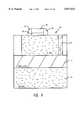
- FIG. 2is a cross-sectional view of the first embodiment of the invention taken along the line 2--2 in FIG. 1.
- the depth of the semiconductor connector 18may also be varied. As shown in FIG. 2, the depth of the semiconductor connector plug 18 is great enough to completely penetrate the underlying insulating layer 12 and contact the substrate 14.
- substrate 14is silicon.
- the silicon substrate 14may be used to interconnect all of the connector plugs for all of the individual cells in the photosensitive device.
Landscapes
- Solid State Image Pick-Up Elements (AREA)
Abstract
Description
Claims (10)
Priority Applications (3)
| Application Number | Priority Date | Filing Date | Title |
|---|---|---|---|
| US09/004,429US5877521A (en) | 1998-01-08 | 1998-01-08 | SOI active pixel cell design with grounded body contact |
| JP11000073AJP3065597B2 (en) | 1998-01-08 | 1999-01-04 | Photosensitive element and method of manufacturing the same |
| US09/231,068US6258636B1 (en) | 1998-01-08 | 1999-01-14 | SOI active pixel cell design with grounded body contact |
Applications Claiming Priority (1)
| Application Number | Priority Date | Filing Date | Title |
|---|---|---|---|
| US09/004,429US5877521A (en) | 1998-01-08 | 1998-01-08 | SOI active pixel cell design with grounded body contact |
Related Child Applications (1)
| Application Number | Title | Priority Date | Filing Date |
|---|---|---|---|
| US09/231,068DivisionUS6258636B1 (en) | 1998-01-08 | 1999-01-14 | SOI active pixel cell design with grounded body contact |
Publications (1)
| Publication Number | Publication Date |
|---|---|
| US5877521Atrue US5877521A (en) | 1999-03-02 |
Family
ID=21710755
Family Applications (2)
| Application Number | Title | Priority Date | Filing Date |
|---|---|---|---|
| US09/004,429Expired - LifetimeUS5877521A (en) | 1998-01-08 | 1998-01-08 | SOI active pixel cell design with grounded body contact |
| US09/231,068Expired - LifetimeUS6258636B1 (en) | 1998-01-08 | 1999-01-14 | SOI active pixel cell design with grounded body contact |
Family Applications After (1)
| Application Number | Title | Priority Date | Filing Date |
|---|---|---|---|
| US09/231,068Expired - LifetimeUS6258636B1 (en) | 1998-01-08 | 1999-01-14 | SOI active pixel cell design with grounded body contact |
Country Status (2)
| Country | Link |
|---|---|
| US (2) | US5877521A (en) |
| JP (1) | JP3065597B2 (en) |
Cited By (17)
| Publication number | Priority date | Publication date | Assignee | Title |
|---|---|---|---|---|
| US6015745A (en)* | 1998-05-18 | 2000-01-18 | International Business Machines Corporation | Method for semiconductor fabrication |
| WO2000021280A1 (en)* | 1998-10-07 | 2000-04-13 | California Institute Of Technology | Silicon-on-insulator (soi) active pixel sensors with the photosites implemented in the substrate |
| US6351003B1 (en)* | 1998-04-22 | 2002-02-26 | Matsushita Electric Industrial Co., Ltd. | Solid-state imaging device and manufacturing method therefor |
| US6387742B2 (en)* | 2000-02-28 | 2002-05-14 | International Business Machines Corporation | Thermal conductivity enhanced semiconductor structures and fabrication processes |
| US6518115B2 (en)* | 1999-06-28 | 2003-02-11 | Hyundai Electronics Industries Co., Ltd. | CMOS image sensor and method for fabricating the same |
| US6538299B1 (en) | 2000-10-03 | 2003-03-25 | International Business Machines Corporation | Silicon-on-insulator (SOI) trench photodiode |
| US6642561B2 (en)* | 2000-05-16 | 2003-11-04 | Minolta Co., Ltd. | Solid imaging device and method for manufacturing the same |
| US6660616B2 (en)* | 2001-01-31 | 2003-12-09 | Texas Instruments Incorporated | P-i-n transit time silicon-on-insulator device |
| US6930336B1 (en)* | 2001-06-18 | 2005-08-16 | Foveon, Inc. | Vertical-color-filter detector group with trench isolation |
| US20060054972A1 (en)* | 2002-06-12 | 2006-03-16 | Silvia Kronmueller | Component and method for producing the same |
| US20070108485A1 (en)* | 2005-02-23 | 2007-05-17 | Adkisson James W | Image sensor cells |
| US20080011942A1 (en)* | 2003-09-08 | 2008-01-17 | Micron Technology, Inc. | Cmos image sensor with photo diode gate |
| US20080217718A1 (en)* | 2007-03-06 | 2008-09-11 | Micron Technology, Inc. | Method, apparatus, and system to reduce ground resistance in a pixel array |
| US20100097506A1 (en)* | 2007-03-30 | 2010-04-22 | Yusuke Hashimoto | Image pickup device, spatial information detecting apparatus using the same device and method for taking out received -light output from the same device |
| US20100155787A1 (en)* | 1998-03-19 | 2010-06-24 | Canon Kabushiki Kaisha | Solid state image pickup device and manufacturing method therefor |
| US20170207270A1 (en)* | 2016-01-15 | 2017-07-20 | Semiconductor Manufacturing International (Shanghai) Corporation | Method of manufacturing a cmos image sensor |
| US11121169B2 (en)* | 2019-06-25 | 2021-09-14 | Omnivision Technologies, Inc. | Metal vertical transfer gate with high-k dielectric passivation lining |
Families Citing this family (18)
| Publication number | Priority date | Publication date | Assignee | Title |
|---|---|---|---|---|
| JP4725673B2 (en)* | 1999-02-09 | 2011-07-13 | ソニー株式会社 | Solid-state imaging device and manufacturing method thereof |
| KR100562667B1 (en)* | 2000-08-31 | 2006-03-20 | 매그나칩 반도체 유한회사 | Image sensor and manufacturing method |
| KR100748314B1 (en)* | 2001-06-28 | 2007-08-09 | 매그나칩 반도체 유한회사 | Image sensor and its manufacturing method |
| KR100748324B1 (en)* | 2001-06-28 | 2007-08-09 | 매그나칩 반도체 유한회사 | Manufacturing Method of Image Sensor |
| KR100790286B1 (en)* | 2001-06-28 | 2008-01-02 | 매그나칩 반도체 유한회사 | Image sensor manufacturing method |
| KR100776150B1 (en)* | 2001-10-23 | 2007-11-15 | 매그나칩 반도체 유한회사 | Image sensor manufacturing method |
| KR100790212B1 (en)* | 2001-11-22 | 2008-01-02 | 매그나칩 반도체 유한회사 | Manufacturing Method of CMOS Image Sensor |
| KR100838466B1 (en)* | 2001-12-27 | 2008-06-16 | 매그나칩 반도체 유한회사 | Highly integrated image sensor manufacturing method |
| KR100776151B1 (en)* | 2001-12-27 | 2007-11-16 | 매그나칩 반도체 유한회사 | Highly integrated image sensor manufacturing method |
| KR100766675B1 (en)* | 2001-12-28 | 2007-10-15 | 매그나칩 반도체 유한회사 | Image sensor manufacturing method for reducing dark signal |
| WO2006008746A2 (en)* | 2004-07-22 | 2006-01-26 | Yissum Research Development Company Of The Hebrew University Of Jerusalem | Integrated active pixel sensor and method of its fabrication |
| JP2006054252A (en)* | 2004-08-10 | 2006-02-23 | Sony Corp | Solid state imaging apparatus |
| DE102004060365B4 (en)* | 2004-12-15 | 2009-03-19 | Austriamicrosystems Ag | Semiconductor junction device and method of manufacture |
| JP5272281B2 (en)* | 2005-09-22 | 2013-08-28 | ソニー株式会社 | Solid-state imaging device, manufacturing method thereof, and camera |
| DE102005059034B4 (en)* | 2005-12-10 | 2007-10-11 | X-Fab Semiconductor Foundries Ag | SOI isolation structures grave |
| KR100781920B1 (en)* | 2006-08-16 | 2007-12-04 | (주)실리콘화일 | Image signal pickup pixel and manufacturing method thereof |
| DE102007007584A1 (en)* | 2006-12-29 | 2008-07-03 | Osram Opto Semiconductors Gmbh | Semiconductor detector arrangement for use as back-illuminated multipin-photo detectors or charge coupled devices sensors, has multiple regions of semiconductor substrate spatial assigned to semiconductor structures |
| US9918429B1 (en) | 2013-05-07 | 2018-03-20 | John T. Di Lallo | Ergonomic weed trimmer |
Citations (9)
| Publication number | Priority date | Publication date | Assignee | Title |
|---|---|---|---|---|
| US4006458A (en)* | 1976-02-09 | 1977-02-01 | Rockwell International Corporation | Detector circuit |
| US5008723A (en)* | 1989-12-29 | 1991-04-16 | Kopin Corporation | MOS thin film transistor |
| US5145802A (en)* | 1991-11-12 | 1992-09-08 | United Technologies Corporation | Method of making SOI circuit with buried connectors |
| US5358879A (en)* | 1993-04-30 | 1994-10-25 | Loral Federal Systems Company | Method of making gate overlapped lightly doped drain for buried channel devices |
| US5559368A (en)* | 1994-08-30 | 1996-09-24 | The Regents Of The University Of California | Dynamic threshold voltage mosfet having gate to body connection for ultra-low voltage operation |
| US5572045A (en)* | 1990-11-15 | 1996-11-05 | Seiko Instruments Inc. | Light valve device using semiconductive composite substrate |
| US5587596A (en)* | 1995-09-20 | 1996-12-24 | National Semiconductor Corporation | Single MOS transistor active pixel sensor cell with automatic anti-blooming and wide dynamic range |
| US5614744A (en)* | 1995-08-04 | 1997-03-25 | National Semiconductor Corporation | CMOS-based, low leakage active pixel array with anti-blooming isolation |
| US5789774A (en)* | 1996-03-01 | 1998-08-04 | Foveonics, Inc. | Active pixel sensor cell that minimizes leakage current |
- 1998
- 1998-01-08USUS09/004,429patent/US5877521A/ennot_activeExpired - Lifetime
- 1999
- 1999-01-04JPJP11000073Apatent/JP3065597B2/ennot_activeExpired - Fee Related
- 1999-01-14USUS09/231,068patent/US6258636B1/ennot_activeExpired - Lifetime
Patent Citations (9)
| Publication number | Priority date | Publication date | Assignee | Title |
|---|---|---|---|---|
| US4006458A (en)* | 1976-02-09 | 1977-02-01 | Rockwell International Corporation | Detector circuit |
| US5008723A (en)* | 1989-12-29 | 1991-04-16 | Kopin Corporation | MOS thin film transistor |
| US5572045A (en)* | 1990-11-15 | 1996-11-05 | Seiko Instruments Inc. | Light valve device using semiconductive composite substrate |
| US5145802A (en)* | 1991-11-12 | 1992-09-08 | United Technologies Corporation | Method of making SOI circuit with buried connectors |
| US5358879A (en)* | 1993-04-30 | 1994-10-25 | Loral Federal Systems Company | Method of making gate overlapped lightly doped drain for buried channel devices |
| US5559368A (en)* | 1994-08-30 | 1996-09-24 | The Regents Of The University Of California | Dynamic threshold voltage mosfet having gate to body connection for ultra-low voltage operation |
| US5614744A (en)* | 1995-08-04 | 1997-03-25 | National Semiconductor Corporation | CMOS-based, low leakage active pixel array with anti-blooming isolation |
| US5587596A (en)* | 1995-09-20 | 1996-12-24 | National Semiconductor Corporation | Single MOS transistor active pixel sensor cell with automatic anti-blooming and wide dynamic range |
| US5789774A (en)* | 1996-03-01 | 1998-08-04 | Foveonics, Inc. | Active pixel sensor cell that minimizes leakage current |
Cited By (35)
| Publication number | Priority date | Publication date | Assignee | Title |
|---|---|---|---|---|
| US20100155787A1 (en)* | 1998-03-19 | 2010-06-24 | Canon Kabushiki Kaisha | Solid state image pickup device and manufacturing method therefor |
| US8138528B2 (en)* | 1998-03-19 | 2012-03-20 | Canon Kabushiki Kaisha | Solid state image pickup device and manufacturing method therefor |
| US8395193B2 (en) | 1998-03-19 | 2013-03-12 | Canon Kabushiki Kaisha | Solid state image pickup device and manufacturing method therefor |
| US9257479B2 (en) | 1998-03-19 | 2016-02-09 | Canon Kabushiki Kaisha | Solid state image pickup device and manufacturing method therefor |
| US6351003B1 (en)* | 1998-04-22 | 2002-02-26 | Matsushita Electric Industrial Co., Ltd. | Solid-state imaging device and manufacturing method therefor |
| US6362019B1 (en) | 1998-04-22 | 2002-03-26 | Matsushita Electric Industrial Co., Ltd. | Solid-state imaging device and manufacturing method therefor |
| US6015745A (en)* | 1998-05-18 | 2000-01-18 | International Business Machines Corporation | Method for semiconductor fabrication |
| US6838301B2 (en) | 1998-10-07 | 2005-01-04 | California Institute Of Technology | Silicon-on-insulator (SOI) active pixel sensors with the photosite implemented in the substrate |
| WO2000021280A1 (en)* | 1998-10-07 | 2000-04-13 | California Institute Of Technology | Silicon-on-insulator (soi) active pixel sensors with the photosites implemented in the substrate |
| US6380572B1 (en) | 1998-10-07 | 2002-04-30 | California Institute Of Technology | Silicon-on-insulator (SOI) active pixel sensors with the photosite implemented in the substrate |
| US20020121655A1 (en)* | 1998-10-07 | 2002-09-05 | California Institute Of Technology | Silicon-on-insulator (SOI) active pixel sensors with the photosites implemented in the substrate |
| US6518115B2 (en)* | 1999-06-28 | 2003-02-11 | Hyundai Electronics Industries Co., Ltd. | CMOS image sensor and method for fabricating the same |
| US6387742B2 (en)* | 2000-02-28 | 2002-05-14 | International Business Machines Corporation | Thermal conductivity enhanced semiconductor structures and fabrication processes |
| US6642561B2 (en)* | 2000-05-16 | 2003-11-04 | Minolta Co., Ltd. | Solid imaging device and method for manufacturing the same |
| WO2002029903A3 (en)* | 2000-10-03 | 2003-10-16 | Ibm | Silicon-on-insulator (soi) trench photodiode and method of forming same |
| US6538299B1 (en) | 2000-10-03 | 2003-03-25 | International Business Machines Corporation | Silicon-on-insulator (SOI) trench photodiode |
| US6660616B2 (en)* | 2001-01-31 | 2003-12-09 | Texas Instruments Incorporated | P-i-n transit time silicon-on-insulator device |
| US6930336B1 (en)* | 2001-06-18 | 2005-08-16 | Foveon, Inc. | Vertical-color-filter detector group with trench isolation |
| US20060054972A1 (en)* | 2002-06-12 | 2006-03-16 | Silvia Kronmueller | Component and method for producing the same |
| US7382031B2 (en)* | 2002-06-12 | 2008-06-03 | Robert Bosch Gmbh | Component including a fixed element that is in a silicon layer and is mechanically connected to a substrate via an anchoring element and method for its manufacture |
| US20080011942A1 (en)* | 2003-09-08 | 2008-01-17 | Micron Technology, Inc. | Cmos image sensor with photo diode gate |
| US7557335B2 (en)* | 2003-09-08 | 2009-07-07 | Aptina Imaging Corporation | CMOS image sensor with photo diode gate |
| US7491992B2 (en)* | 2005-02-23 | 2009-02-17 | International Business Machines Corporation | Image sensor cells |
| US20070108485A1 (en)* | 2005-02-23 | 2007-05-17 | Adkisson James W | Image sensor cells |
| US20080217718A1 (en)* | 2007-03-06 | 2008-09-11 | Micron Technology, Inc. | Method, apparatus, and system to reduce ground resistance in a pixel array |
| US7728279B2 (en) | 2007-03-06 | 2010-06-01 | Aptina Imaging Corporation | Methods, devices, and systems related to pixel arrays |
| US7459668B2 (en) | 2007-03-06 | 2008-12-02 | Micron Technology, Inc. | Method, apparatus, and system to reduce ground resistance in a pixel array |
| GB2468375A (en)* | 2007-03-06 | 2010-09-08 | Aptina Imaging Corp | Method,apparatus, and system to reduce ground resistance in a pixel array |
| WO2008109273A1 (en)* | 2007-03-06 | 2008-09-12 | Aptina Imaging Corporation | Method, apparatus, and system to reduce ground resistance in a pixel array |
| US20090067702A1 (en)* | 2007-03-06 | 2009-03-12 | Micron Technology, Inc. | Methods, devices, and systems related to pixel arrays |
| US8264577B2 (en)* | 2007-03-30 | 2012-09-11 | Panasonic Corporation | Image pickup device, spatial information detecting apparatus using the same device and method for taking out received-light output from the same device |
| US20100097506A1 (en)* | 2007-03-30 | 2010-04-22 | Yusuke Hashimoto | Image pickup device, spatial information detecting apparatus using the same device and method for taking out received -light output from the same device |
| US20170207270A1 (en)* | 2016-01-15 | 2017-07-20 | Semiconductor Manufacturing International (Shanghai) Corporation | Method of manufacturing a cmos image sensor |
| US10784303B2 (en)* | 2016-01-15 | 2020-09-22 | Semiconductor Manufacturing International (Shanghai) Corporation | Method of manufacturing a CMOS image sensor |
| US11121169B2 (en)* | 2019-06-25 | 2021-09-14 | Omnivision Technologies, Inc. | Metal vertical transfer gate with high-k dielectric passivation lining |
Also Published As
| Publication number | Publication date |
|---|---|
| JP3065597B2 (en) | 2000-07-17 |
| JPH11251569A (en) | 1999-09-17 |
| US6258636B1 (en) | 2001-07-10 |
Similar Documents
| Publication | Publication Date | Title |
|---|---|---|
| US5877521A (en) | SOI active pixel cell design with grounded body contact | |
| US11205672B2 (en) | Image sensor | |
| US10804304B2 (en) | Image sensors | |
| EP1394858B1 (en) | Semiconductor device for reading signal from photodiode via transistors | |
| EP1004140B1 (en) | A well to substrate photodiode for use in a cmos sensor on a salicide process | |
| EP1668701B1 (en) | IMAGE SENSOR HAVING PINNED FLOATING DIFFUSION DIODE and its method of manufacturing | |
| US7491990B2 (en) | CMOS image sensors for preventing optical crosstalk | |
| US5463232A (en) | Solid-state imaging device with internal smear eliminator | |
| JP4604296B2 (en) | Solid-state imaging device and manufacturing method thereof | |
| TWI711171B (en) | Image sensor and method for forming the same | |
| CN100449769C (en) | CMOS image sensor and method of manufacturing the same | |
| KR20200035821A (en) | Pixel device on deep trench isolation (dti) structure for image sensor | |
| US11574947B2 (en) | Method and image sensor with vertical transfer gate and buried backside-illuminated photodiodes | |
| JP2004039832A (en) | Photoelectric converter and its manufacturing method | |
| US20060255381A1 (en) | Pixel with gate contacts over active region and method of forming same | |
| US20010023949A1 (en) | SOI active pixel cell design with grounded body contact | |
| US8173480B2 (en) | Image sensor and method for manufacturing the same | |
| US4912537A (en) | Image sensing array with charge isolation | |
| JP4725674B2 (en) | Solid-state imaging device and manufacturing method thereof | |
| KR100956193B1 (en) | CMOS image sensor with improved transfer efficiency and its manufacturing method | |
| KR102645312B1 (en) | Backside illumination image sensor and method of manufacturing the same | |
| CN120603344A (en) | CMOS image sensor and method of forming the same | |
| CN114256283A (en) | CMOS image sensor and method of manufacturing the same |
Legal Events
| Date | Code | Title | Description |
|---|---|---|---|
| AS | Assignment | Owner name:INTERNATIONAL BUSINESS MACHINES CORPORATION, NEW Y Free format text:ASSIGNMENT OF ASSIGNORS INTEREST;ASSIGNORS:JOHNSON, JEFFREY B.;WONG, HON-SUM P.;REEL/FRAME:008929/0592;SIGNING DATES FROM 19971107 TO 19971215 | |
| STCF | Information on status: patent grant | Free format text:PATENTED CASE | |
| FPAY | Fee payment | Year of fee payment:4 | |
| FPAY | Fee payment | Year of fee payment:8 | |
| FPAY | Fee payment | Year of fee payment:12 | |
| AS | Assignment | Owner name:GLOBALFOUNDRIES U.S. 2 LLC, NEW YORK Free format text:ASSIGNMENT OF ASSIGNORS INTEREST;ASSIGNOR:INTERNATIONAL BUSINESS MACHINES CORPORATION;REEL/FRAME:036550/0001 Effective date:20150629 | |
| AS | Assignment | Owner name:GLOBALFOUNDRIES INC., CAYMAN ISLANDS Free format text:ASSIGNMENT OF ASSIGNORS INTEREST;ASSIGNORS:GLOBALFOUNDRIES U.S. 2 LLC;GLOBALFOUNDRIES U.S. INC.;REEL/FRAME:036779/0001 Effective date:20150910 | |
| AS | Assignment | Owner name:GLOBALFOUNDRIES U.S. INC., NEW YORK Free format text:RELEASE BY SECURED PARTY;ASSIGNOR:WILMINGTON TRUST, NATIONAL ASSOCIATION;REEL/FRAME:056987/0001 Effective date:20201117 |