US5875143A - Dynamic memory device with refresh circuit and refresh method - Google Patents
Dynamic memory device with refresh circuit and refresh methodDownload PDFInfo
- Publication number
- US5875143A US5875143AUS08/976,835US97683597AUS5875143AUS 5875143 AUS5875143 AUS 5875143AUS 97683597 AUS97683597 AUS 97683597AUS 5875143 AUS5875143 AUS 5875143A
- Authority
- US
- United States
- Prior art keywords
- address
- addresses
- decoder
- storage elements
- refresh
- Prior art date
- Legal status (The legal status is an assumption and is not a legal conclusion. Google has not performed a legal analysis and makes no representation as to the accuracy of the status listed.)
- Expired - Lifetime
Links
Images

Classifications
- G—PHYSICS
- G11—INFORMATION STORAGE
- G11C—STATIC STORES
- G11C11/00—Digital stores characterised by the use of particular electric or magnetic storage elements; Storage elements therefor
- G11C11/21—Digital stores characterised by the use of particular electric or magnetic storage elements; Storage elements therefor using electric elements
- G11C11/34—Digital stores characterised by the use of particular electric or magnetic storage elements; Storage elements therefor using electric elements using semiconductor devices
- G11C11/40—Digital stores characterised by the use of particular electric or magnetic storage elements; Storage elements therefor using electric elements using semiconductor devices using transistors
- G11C11/401—Digital stores characterised by the use of particular electric or magnetic storage elements; Storage elements therefor using electric elements using semiconductor devices using transistors forming cells needing refreshing or charge regeneration, i.e. dynamic cells
- G11C11/4063—Auxiliary circuits, e.g. for addressing, decoding, driving, writing, sensing or timing
- G11C11/407—Auxiliary circuits, e.g. for addressing, decoding, driving, writing, sensing or timing for memory cells of the field-effect type
- G—PHYSICS
- G11—INFORMATION STORAGE
- G11C—STATIC STORES
- G11C11/00—Digital stores characterised by the use of particular electric or magnetic storage elements; Storage elements therefor
- G11C11/21—Digital stores characterised by the use of particular electric or magnetic storage elements; Storage elements therefor using electric elements
- G11C11/34—Digital stores characterised by the use of particular electric or magnetic storage elements; Storage elements therefor using electric elements using semiconductor devices
- G11C11/40—Digital stores characterised by the use of particular electric or magnetic storage elements; Storage elements therefor using electric elements using semiconductor devices using transistors
- G11C11/401—Digital stores characterised by the use of particular electric or magnetic storage elements; Storage elements therefor using electric elements using semiconductor devices using transistors forming cells needing refreshing or charge regeneration, i.e. dynamic cells
- G11C11/406—Management or control of the refreshing or charge-regeneration cycles
- G11C11/40622—Partial refresh of memory arrays
- G—PHYSICS
- G11—INFORMATION STORAGE
- G11C—STATIC STORES
- G11C11/00—Digital stores characterised by the use of particular electric or magnetic storage elements; Storage elements therefor
- G11C11/21—Digital stores characterised by the use of particular electric or magnetic storage elements; Storage elements therefor using electric elements
- G11C11/34—Digital stores characterised by the use of particular electric or magnetic storage elements; Storage elements therefor using electric elements using semiconductor devices
- G11C11/40—Digital stores characterised by the use of particular electric or magnetic storage elements; Storage elements therefor using electric elements using semiconductor devices using transistors
- G11C11/401—Digital stores characterised by the use of particular electric or magnetic storage elements; Storage elements therefor using electric elements using semiconductor devices using transistors forming cells needing refreshing or charge regeneration, i.e. dynamic cells
- G11C11/406—Management or control of the refreshing or charge-regeneration cycles
- G—PHYSICS
- G11—INFORMATION STORAGE
- G11C—STATIC STORES
- G11C2211/00—Indexing scheme relating to digital stores characterized by the use of particular electric or magnetic storage elements; Storage elements therefor
- G11C2211/401—Indexing scheme relating to cells needing refreshing or charge regeneration, i.e. dynamic cells
- G11C2211/406—Refreshing of dynamic cells
- G11C2211/4067—Refresh in standby or low power modes
Definitions
- the present inventionrelates to a dynamic memory device, and a method to refresh dynamic memory devices, as for example but not limited to a Dynamic Random Access Memory (DRAM).
- DRAMDynamic Random Access Memory
- Dynamic memory devicessuch as DRAM need to be refreshed. This consumes energy. In many systems energy consumption is very crucial for performance, and the power used for refreshing should be reduced.
- Energy consumptioncan be reduced by using a memory that consists not only of a DRAM but also of a less power consuming static memory (SRAM).
- SRAMstatic memory
- During standby mode critical datacan be stored in the SRAM, and the DRAM can be switched off and not refreshed.
- Providing an SRAMleads to additional cost and space. Moreover, two different memory access cycles are required.
- U.S. Pat. No. 5,331,601describes a memory device that alters the input refresh addresses to access fewer memory cells to save power, or to address more memory cells to decrease the refresh time.
- the circuitcontains a simple transistor configuration that blocks certain address bits, then substitutes active bits in their place to the address decoder.
- the circuitalso includes a controller that is responsive to the memory device entering the refresh mode. When the device is used in refresh mode, the address bits may be passed unblocked to the address decoder for full user control.
- European patent application 488 593relates to the stability of the refresh in case the power supply fails.
- FIG. 1shows a schematic block diagram of prior art dynamic memory device 101.
- Dynamic memory device 101comprises memory array 110, address generator 112 and decoder 114. The combination of address generator 112 and decoder 114 is referred to as refresh circuit 130. As shown in FIG. 1, dynamic memory device 101 also comprises data terminal 120 and optional terminal 116.
- Memory array 110comprises a multitude of storage elements 111 and data accessing means 118. Data accessing means 118 is provided to write, read and update data which is stored in storage elements 111. Data accessing means 118 is connected to storage elements 111 and to data terminal 120.
- a physical group of storage elements 111 in memory array 110is referred to as block 113.
- Blocks 113are logically designated by A 1 , A i . . . A n .
- the number of blocks 113is n.
- Block addresses a 1 , a i . . . a nare logically assigned to blocks A 1 , A i . . . A n .
- Outputs 117 of decoder 114are connected to storage elements 111 of corresponding blocks 113.
- Address generator 112is connected to decoder 114 and generates block addresses 119 (a 1 , a i . . . a n ) corresponding to blocks 113 (A 1 , A i . . . A n ).
- Dynamic memory device 101can be connected to other components via data terminal 120 or optional terminal 116.
- Optional terminal 116can provide control signal 121 for address generator 112.
- control signal 121can be a clock signal.
- address generator 112In one refresh cycle, address generator 112 generates block addresses 119 (a 1 , a i . . . a n ) for all blocks 113 (A 1 , A i . . . A n ) of memory array 110.
- Block addresses a 1 , a i . . . a ncan have, for example, ascending or descending values.
- Block addresses a 1 , a i . . . a nare supplied to decoder 114. Decoder 114 sends refresh signals 115 to corresponding blocks 113 on memory array 110.
- Decoder 114Upon receiving refresh signal 115 the information of all storage elements 111 of one block 113 is updated by data accessing means 118, thus each block 113 is refreshed.
- address generator 112resets automatically and the cycle can start again when a clock signal is available.
- the clock signalcan be supplied as control signal 121 via optional terminal 116. It can also be generated by address generator 112
- a DRAMthat data is stored in an array comprising memory cells which are arranged for example in rows.
- the memory cellscorrespond to storage elements 111, the rows to blocks 113, a counter to address generator 112, a row decoder to decoder 114, and data accessing means 118 comprises charge detection circuits for reading the information.
- Row addressesare generated in the counter and supplied to the row decoder.
- the row decoderis connected to each row via outputs 117.
- the signals at the outputs of the row decoderare the above mentioned refresh signals 115. When refresh signal 115 is applied to a particular row, the information of every single memory cell of that particular row is read and the capacitor of that memory cell is recharged if required, thus that row is refreshed.
- the memory cellsare arranged in 1024 rows designated as A 1 . . . A 1024 .
- the row decoderis connected to each row and supplies above mentioned refresh signals 115 to the rows.
- a charge detection circuitwhich is part of data accessing means 118. If the memory cell is charged, than it is recharged. That means that all memory cells with charged capacitors (e.g., representing the bit "1”) are recharged, and these with uncharged capacitors (e.g., representing the bit "0") are not recharged.
- a DRAMusually also includes data accessing means 118 to read the information of each memory cell. Additional addresses such as, for example, column addresses are required to access each memory cell. That additional addresses can be supplied via data terminal 120.
- the inventionprovides an improved refresh circuit for dynamic memory devices and a method for refreshing such devices that reduces or overcomes the above mentioned problems of prior art.
- FIG. 1shows a schematic diagram of a dynamic memory device as known in prior art
- FIG. 2shows a schematic diagram of a dynamic memory device with modified refresh circuit according to a preferred embodiment of the invention.
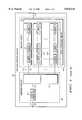
- FIG. 2shows a schematic diagram of dynamic memory device 201 with modified refresh circuit 230 according to a preferred embodiment of the invention.
- dynamic memory device 201comprises memory array 210, address generator 212 and decoder 214. Additionally, dynamic memory device 201 comprises reference register 222 or other storage means and control logic 224. Dynamic memory device 201 also comprises data terminal 220 and optional terminals 216, 226, 236.
- signal provider 260The combination of address generator 212 and decoder 214 is referred to as signal provider 260.
- the combination of reference register 222 and control logic 224is referred to as signal controller 270.
- Signal provider 260 and signal controller 270form refresh circuit 230.
- memory array 210comprises a multitude of storage elements 211 and data accessing means 218.
- Data accessing means 218is provided to write, read and update data which is stored in storage elements 211.
- Data accessing means 218is connected to storage elements 211 and to data terminal 220.
- Optional terminal 216can provide control signal 221 for address generator 212.
- control signal 221can be a clock signal.
- a physical group of storage elements 211 in memory array 210is referred to as block 213.
- Each block 213is logically designated by A 1 , A i . . . A n .
- the number of blocks 213is n.
- Block addresses 219 a 1 , a i . . . a nare logically assigned to blocks A 1 , A i . . . A n .
- Outputs 217 of decoder 214are connected to storage elements 211 of corresponding blocks 213.
- the reference numbers 101/201, 110/210, 111/211, 112/212, 113/213, 114/214, 115/215, 116/216, 117/217, 118/218, 119/219, 120/220, 121/221, 130/230stand for analogous components or signals. However, their operation or function is different as a consequence of the embodiment which will be explained in detail referring to FIG. 2.
- Reference register 222is used to store a reference address a r .
- reference address a ris indicated by number 223.
- the reference address a rcan be provided to reference register 222 by optional terminal 226.
- Control logic 224is connected at input 227 to address generator 212 and at input 229 to reference register 222.
- Decoder 214is equipped with ENABLE-input 234 connected to output 225 of control logic 224.
- Optional link 250can be provided between memory array 210 and reference register 222.
- Optional terminal 236can be provided for feeding signals to control logic 224.
- Address generator 212continually supplies block addresses 219 (a 1 , a i . . . a n ) to decoder 214.
- the constant reference address a rappears at input 229 of control logic 224.
- control logic 224At input 227 of control logic 224 an address a i of the changing addresses a 1 , a i . . . a n from address generator 212 is present.
- Control logic 224compares this address a i with the reference address a r and switches decoder 214 ON and OFF according to a logical function f(a i , a r ) implemented in control logic 224.
- the logical function f(a i , a r )can be expressed by terms such as greater or smaller than, odd or even, modulo, etc. In that way, decoder 214 sends refresh signals 215 to memory array 210 only when it is enabled by control logic 224 at ENABLE-input 234.
- the reference address a r or information to produce itcan be supplied to reference register 222 via optional terminal 226 or it can be stored internally.
- the logical functioncan be implemented in control logic 224, but any means for supplying the logical function f(a i , a r ) to control logic 224 can also be used.
- the logical function f(a i , a r )can be supplied to control logic 224 via optional terminal 236 or it can be supplied via optional terminal 226 or optional terminal 216 or a combination thereof, or it can be stored within dynamic memory device 201.
- control logic 224is a comparator.
- Address generator 212generates addresses a i which are in this example numbers from 1 to 1024 and returns to 1. When these addresses are smaller or equal to 512 than decoder 214 is enabled and rows A 1 to A 512 are refreshed.
- address generator 212counts further from 513 to 1024, but decoder 214 is disabled and rows A 513 ,A 514 . . . A 1024 are not refreshed. In that example, refreshed rows A 1 ,A 2 . . . A 512 are contiguous. This is convenient but not essential. Rows A 513 , A 514 . . . A 1024 which are not refreshed can also be contiguous.
- address generator 212with the generation of all block addresses a 1 , a i . . . a n in one cycle can be the same as in prior art.
- Address generator 212 and reference register 222are independent.
- the number of blocks 213 in memory array 210 to be refresheddepends only on the reference address a r of reference register 222 and of the logical function f(a i , a r ) which commands control logic 224.
- the present invention of FIG. 2allows one to divide the total number of storage elements 211 into two sets: a first set of storage elements 211 to be refreshed, and a second set of storage elements 211 not to be refreshed.
- the term "set”is also applicable to blocks 213: storage elements 211 of the first set of blocks 213 are to be refreshed, and storage elements 211 of the second set of blocks 213 are not to be refreshed.
- refresh circuit 130 of prior artallows only full refresh of an array; and refresh circuit 230 of the present invention allows not only full but also partial refresh of an memory array of storage elements. It is also included in the present invention that reference address a r and logical function f(a i , a r ) can be supplied from outside dynamic memory device 201.
- reference register 222can be set to a certain value a r0 , preferably equal to but not excluding the lowest address a 1 or the highest address a n of address generator 212. Then, memory array 210 can store the maximum amount of data because it will be refreshed completely on each refresh cycle.
- the above mentioned first setcontains all blocks 213 and the second set is empty.
- the present inventionis not limited merely to the use of one address generator 212, reference register 222 or control logic 224. Additional units can be used and combined in order to specify blocks 213 to be refreshed more flexibly. This is especially important if dynamic memory device 201 is a Content Addressable Memory in which the blocks to be refreshed need to be controlled by the system in which dynamic memory device 201 is used.
- the reference address a r as well as the logical function f(a i , a r ) and therefore blocks 213 to be refreshedcan be determined by software and adjusted to the requirements of the system and of each application.
- reference register 222can be set to a certain value a r fix. That value can not be changed from outside dynamic memory device 201.
- control signal 237is provided at optional terminal 236. Depending on control signal 237 memory array 210 is refreshed fully or only partially refreshed.
- reference register 222is coupled by optional link 250 directly to data accessing means 218.
- the reference address a ris part of the data stored in the DRAM.
- the applicationsare not limited to such systems.
- There are many other stationary and remote systems where the power source is difficult to maintain or even impossible to replaceas, for example, in solar or wind powered transmitters, remote earthquake or temperature sensors, emergency beacons, and in satellites.
- reducing size and power consumption of an implantable medical devicehas an appreciable advantage for the patient, since the battery needs to be exchanged less often or not at all.
- dynamic memory devicescan be used in applications from which they had been previously excluded.
- the space which the hardware of the inventive refresh circuit requiresis very small compared to the other elements.
- As the improved hardwareis compatible with existing software, there is no need to modify software at the same time as introducing the present invention.
- the use of expensive hardware such as for static memory devicescan be significantly reduced or avoided, thus increasing reliability and cost saving.
Landscapes
- Engineering & Computer Science (AREA)
- Microelectronics & Electronic Packaging (AREA)
- Computer Hardware Design (AREA)
- Dram (AREA)
Abstract
Description
Claims (13)
Priority Applications (1)
| Application Number | Priority Date | Filing Date | Title |
|---|---|---|---|
| US08/976,835US5875143A (en) | 1996-07-15 | 1997-11-24 | Dynamic memory device with refresh circuit and refresh method |
Applications Claiming Priority (2)
| Application Number | Priority Date | Filing Date | Title |
|---|---|---|---|
| US68364296A | 1996-07-15 | 1996-07-15 | |
| US08/976,835US5875143A (en) | 1996-07-15 | 1997-11-24 | Dynamic memory device with refresh circuit and refresh method |
Related Parent Applications (1)
| Application Number | Title | Priority Date | Filing Date |
|---|---|---|---|
| US68364296AContinuation | 1996-07-15 | 1996-07-15 |
Publications (1)
| Publication Number | Publication Date |
|---|---|
| US5875143Atrue US5875143A (en) | 1999-02-23 |
Family
ID=24744893
Family Applications (1)
| Application Number | Title | Priority Date | Filing Date |
|---|---|---|---|
| US08/976,835Expired - LifetimeUS5875143A (en) | 1996-07-15 | 1997-11-24 | Dynamic memory device with refresh circuit and refresh method |
Country Status (7)
| Country | Link |
|---|---|
| US (1) | US5875143A (en) |
| EP (1) | EP0820065A3 (en) |
| JP (1) | JPH1069768A (en) |
| KR (1) | KR980011482A (en) |
| IL (1) | IL121044A (en) |
| SG (1) | SG53006A1 (en) |
| TW (1) | TW331644B (en) |
Cited By (25)
| Publication number | Priority date | Publication date | Assignee | Title |
|---|---|---|---|---|
| US6081472A (en)* | 1997-02-18 | 2000-06-27 | Lg Semicon Co., Ltd. | Cell refresh circuit of memory device |
| US6141280A (en)* | 1997-12-30 | 2000-10-31 | Hyundai Electronics Industries Co., Ltd. | Refresh period automatic detecting device for semiconductor memory device, method of automatically detecting refresh period, and refresh period output device |
| US6167484A (en)* | 1998-05-12 | 2000-12-26 | Motorola, Inc. | Method and apparatus for leveraging history bits to optimize memory refresh performance |
| US6570794B1 (en) | 2001-12-27 | 2003-05-27 | Infineon Technologies North America Corp. | Twisted bit-line compensation for DRAM having redundancy |
| US6603694B1 (en) | 2002-02-05 | 2003-08-05 | Infineon Technologies North America Corp. | Dynamic memory refresh circuitry |
| US6608783B2 (en) | 2001-12-27 | 2003-08-19 | Infineon Technologies North America Corp. | Twisted bit-line compensation |
| US6618314B1 (en) | 2002-03-04 | 2003-09-09 | Cypress Semiconductor Corp. | Method and architecture for reducing the power consumption for memory devices in refresh operations |
| US20030206427A1 (en)* | 2001-05-07 | 2003-11-06 | Hyong-Ryol Hwang | System and method for performing partial array self-refresh operation in a semiconductor memory device |
| US6665224B1 (en) | 2002-05-22 | 2003-12-16 | Infineon Technologies Ag | Partial refresh for synchronous dynamic random access memory (SDRAM) circuits |
| US20040017719A1 (en)* | 2002-07-24 | 2004-01-29 | Bell Debra M. | Method and apparatus for saving refresh current |
| US20040057317A1 (en)* | 1990-10-31 | 2004-03-25 | Scott Schaefer | Low power memory module using restricted device activation |
| US6738861B2 (en)* | 2001-09-20 | 2004-05-18 | Intel Corporation | System and method for managing data in memory for reducing power consumption |
| US6862238B1 (en) | 2003-09-25 | 2005-03-01 | Infineon Technologies Ag | Memory system with reduced refresh current |
| US20050078538A1 (en)* | 2003-09-30 | 2005-04-14 | Rainer Hoehler | Selective address-range refresh |
| US20050190625A1 (en)* | 2003-04-24 | 2005-09-01 | Fujitsu Limited | Semiconductor memory |
| US20060133173A1 (en)* | 2004-12-21 | 2006-06-22 | Jain Sandeep K | Method, apparatus, and system for active refresh management |
| US20060245288A1 (en)* | 2005-04-29 | 2006-11-02 | Wolfgang Hokenmaier | Self-refresh circuit with optimized power consumption |
| US20060291311A1 (en)* | 2005-06-10 | 2006-12-28 | Samsung Electronics Co., Ltd. | Memory device for retaining data during power-down mode and method of operating the same |
| US20070002664A1 (en)* | 1999-11-09 | 2007-01-04 | Fujitsu Limited | Semiconductor memory device, and method of controlling the same |
| US20080103634A1 (en)* | 2006-10-30 | 2008-05-01 | Ishmael Santos | Memory module thermal management |
| EP2083423A1 (en)* | 1999-11-09 | 2009-07-29 | Fujitsu Microelectronics Limited | Semiconductor memory device, and method of controlling the same |
| US20100027367A1 (en)* | 2008-08-04 | 2010-02-04 | Micron Technology, Inc. | Row mask addressing |
| US20100208537A1 (en)* | 2009-02-19 | 2010-08-19 | Pelley Iii Perry H | Dynamic random access memory (dram) refresh |
| US8588017B2 (en) | 2010-10-20 | 2013-11-19 | Samsung Electronics Co., Ltd. | Memory circuits, systems, and modules for performing DRAM refresh operations and methods of operating the same |
| US9129702B2 (en) | 2013-08-06 | 2015-09-08 | Samsung Electronics Co., Ltd. | Method of refreshing volatile memory device |
Families Citing this family (11)
| Publication number | Priority date | Publication date | Assignee | Title |
|---|---|---|---|---|
| FI990038L (en) | 1999-01-11 | 2000-07-12 | Nokia Mobile Phones Ltd | Method for refreshing dynamic memory |
| KR100355226B1 (en)* | 1999-01-12 | 2002-10-11 | 삼성전자 주식회사 | DRAM performable selectively self-refresh operation for memory bank |
| JP2001338489A (en)* | 2000-05-24 | 2001-12-07 | Mitsubishi Electric Corp | Semiconductor device |
| US20020138690A1 (en)* | 2001-03-23 | 2002-09-26 | Simmonds Stephen M. | System and method for performing a partial DRAM refresh |
| US20030053361A1 (en)* | 2001-09-20 | 2003-03-20 | Haitao Zhang | EDRAM based architecture |
| KR100424178B1 (en) | 2001-09-20 | 2004-03-24 | 주식회사 하이닉스반도체 | Circuit for internal address generation in semiconductor memory device |
| DE10154770B4 (en)* | 2001-11-08 | 2004-11-18 | Infineon Technologies Ag | Dynamic memory device with a selection device for the selective fading out of unused memory cells during the refresh |
| DE10211570A1 (en)* | 2002-03-15 | 2003-10-09 | Infineon Technologies Ag | Method of running linear store e.g. for processor systems, requires updating used storage zones via driver circuit |
| KR100535071B1 (en)* | 2002-11-07 | 2005-12-07 | 주식회사 하이닉스반도체 | Self refresh apparatus |
| JP2009295274A (en)* | 2009-09-16 | 2009-12-17 | Renesas Technology Corp | Semiconductor device |
| US9159396B2 (en)* | 2011-06-30 | 2015-10-13 | Lattice Semiconductor Corporation | Mechanism for facilitating fine-grained self-refresh control for dynamic memory devices |
Citations (4)
| Publication number | Priority date | Publication date | Assignee | Title |
|---|---|---|---|---|
| US4914630A (en)* | 1987-05-15 | 1990-04-03 | Mitsubishi Denki Kabushiki Kaisha | Refresh arrangement in a block divided memory including a plurality of shift registers |
| EP0488593A2 (en)* | 1990-11-30 | 1992-06-03 | Nec Corporation | Dynamic random access memory device with improved refreshing unit |
| US5247655A (en)* | 1989-11-07 | 1993-09-21 | Chips And Technologies, Inc. | Sleep mode refresh apparatus |
| EP0609577A2 (en)* | 1993-02-04 | 1994-08-10 | United Memories, Inc. | Dram variable row select |
Family Cites Families (4)
| Publication number | Priority date | Publication date | Assignee | Title |
|---|---|---|---|---|
| JPS6313197A (en)* | 1986-07-03 | 1988-01-20 | Nec Corp | Dynamic semiconductor storage device |
| US5283885A (en)* | 1988-09-09 | 1994-02-01 | Werner Hollerbauer | Storage module including a refresh device for storing start and stop refresh addresses |
| US5499213A (en)* | 1992-06-29 | 1996-03-12 | Fujitsu Limited | Semiconductor memory device having self-refresh function |
| US5469559A (en)* | 1993-07-06 | 1995-11-21 | Dell Usa, L.P. | Method and apparatus for refreshing a selected portion of a dynamic random access memory |
- 1997
- 1997-06-09ILIL12104497Apatent/IL121044A/ennot_activeIP Right Cessation
- 1997-06-25EPEP97110375Apatent/EP0820065A3/ennot_activeWithdrawn
- 1997-07-02SGSG1997002347Apatent/SG53006A1/enunknown
- 1997-07-07KRKR1019970031352Apatent/KR980011482A/ennot_activeWithdrawn
- 1997-07-11JPJP9202436Apatent/JPH1069768A/enactivePending
- 1997-07-15TWTW086110014Apatent/TW331644B/ennot_activeIP Right Cessation
- 1997-11-24USUS08/976,835patent/US5875143A/ennot_activeExpired - Lifetime
Patent Citations (4)
| Publication number | Priority date | Publication date | Assignee | Title |
|---|---|---|---|---|
| US4914630A (en)* | 1987-05-15 | 1990-04-03 | Mitsubishi Denki Kabushiki Kaisha | Refresh arrangement in a block divided memory including a plurality of shift registers |
| US5247655A (en)* | 1989-11-07 | 1993-09-21 | Chips And Technologies, Inc. | Sleep mode refresh apparatus |
| EP0488593A2 (en)* | 1990-11-30 | 1992-06-03 | Nec Corporation | Dynamic random access memory device with improved refreshing unit |
| EP0609577A2 (en)* | 1993-02-04 | 1994-08-10 | United Memories, Inc. | Dram variable row select |
Cited By (58)
| Publication number | Priority date | Publication date | Assignee | Title |
|---|---|---|---|---|
| US20040057317A1 (en)* | 1990-10-31 | 2004-03-25 | Scott Schaefer | Low power memory module using restricted device activation |
| US6081472A (en)* | 1997-02-18 | 2000-06-27 | Lg Semicon Co., Ltd. | Cell refresh circuit of memory device |
| US6141280A (en)* | 1997-12-30 | 2000-10-31 | Hyundai Electronics Industries Co., Ltd. | Refresh period automatic detecting device for semiconductor memory device, method of automatically detecting refresh period, and refresh period output device |
| US6167484A (en)* | 1998-05-12 | 2000-12-26 | Motorola, Inc. | Method and apparatus for leveraging history bits to optimize memory refresh performance |
| US8130586B2 (en) | 1999-11-09 | 2012-03-06 | Fujitsu Semiconductor Limited | Semiconductor memory device and method of controlling the same |
| US7688661B2 (en) | 1999-11-09 | 2010-03-30 | Fujitsu Microelectronics Limited | Semiconductor memory device, and method of controlling the same |
| US20070002664A1 (en)* | 1999-11-09 | 2007-01-04 | Fujitsu Limited | Semiconductor memory device, and method of controlling the same |
| US20090010080A1 (en)* | 1999-11-09 | 2009-01-08 | Fujitsu Limited | Semiconductor memory device, and method of controlling the same |
| US7903487B2 (en) | 1999-11-09 | 2011-03-08 | Fujitsu Semiconductor Limited | Semiconductor memory device, and method of controlling the same |
| US7869296B2 (en) | 1999-11-09 | 2011-01-11 | Fujitsu Semiconductor Limited | Semiconductor memory device, and method of controlling the same |
| US20090016142A1 (en)* | 1999-11-09 | 2009-01-15 | Fujitsu Limited | Semiconductor memory device, and method of controlling the same |
| US8619487B2 (en) | 1999-11-09 | 2013-12-31 | Fujitsu Semiconductor Limited | Semiconductor memory device and method of controlling the same |
| EP2083423A1 (en)* | 1999-11-09 | 2009-07-29 | Fujitsu Microelectronics Limited | Semiconductor memory device, and method of controlling the same |
| EP2267723A1 (en)* | 1999-11-09 | 2010-12-29 | Fujitsu Semiconductor Limited | Semiconductor memory device and method of controlling the same |
| EP1256957A3 (en)* | 2001-05-07 | 2004-03-17 | Samsung Electronics Co., Ltd. | System and method for performing partial array self-refresh operation in a semiconductor memory device. |
| US20050041506A1 (en)* | 2001-05-07 | 2005-02-24 | Hyong-Ryol Hwang | System and method for performing partial array self-refresh operation in a semiconductor memory device |
| US6819617B2 (en)* | 2001-05-07 | 2004-11-16 | Samsung Electronics Co., Ltd. | System and method for performing partial array self-refresh operation in a semiconductor memory device |
| US6992943B2 (en) | 2001-05-07 | 2006-01-31 | Samsung Electronics Co., Ltd. | System and method for performing partial array self-refresh operation in a semiconductor memory device |
| US20030206427A1 (en)* | 2001-05-07 | 2003-11-06 | Hyong-Ryol Hwang | System and method for performing partial array self-refresh operation in a semiconductor memory device |
| CN1300801C (en)* | 2001-05-07 | 2007-02-14 | 三星电子株式会社 | Automatic partial-array updating system and method for semiconductor memory |
| US20040268031A1 (en)* | 2001-09-20 | 2004-12-30 | Lawrence Richard H | System and method for managing data in memory for reducing power consumption |
| US6738861B2 (en)* | 2001-09-20 | 2004-05-18 | Intel Corporation | System and method for managing data in memory for reducing power consumption |
| US7380048B2 (en)* | 2001-09-20 | 2008-05-27 | Intel Corporation | System and method for managing data in memory for reducing power consumption |
| US6570794B1 (en) | 2001-12-27 | 2003-05-27 | Infineon Technologies North America Corp. | Twisted bit-line compensation for DRAM having redundancy |
| US6608783B2 (en) | 2001-12-27 | 2003-08-19 | Infineon Technologies North America Corp. | Twisted bit-line compensation |
| DE10304673B4 (en)* | 2002-02-05 | 2010-03-11 | Qimonda Ag | Refresh circuit for dynamic memory |
| US6603694B1 (en) | 2002-02-05 | 2003-08-05 | Infineon Technologies North America Corp. | Dynamic memory refresh circuitry |
| US6618314B1 (en) | 2002-03-04 | 2003-09-09 | Cypress Semiconductor Corp. | Method and architecture for reducing the power consumption for memory devices in refresh operations |
| US7057960B1 (en) | 2002-03-04 | 2006-06-06 | Cypress Semiconductor Corp. | Method and architecture for reducing the power consumption for memory devices in refresh operations |
| US6665224B1 (en) | 2002-05-22 | 2003-12-16 | Infineon Technologies Ag | Partial refresh for synchronous dynamic random access memory (SDRAM) circuits |
| US20040017719A1 (en)* | 2002-07-24 | 2004-01-29 | Bell Debra M. | Method and apparatus for saving refresh current |
| US6778455B2 (en) | 2002-07-24 | 2004-08-17 | Micron Technology, Inc. | Method and apparatus for saving refresh current |
| US7154799B2 (en)* | 2003-04-24 | 2006-12-26 | Fujitsu Limited | Semiconductor memory with single cell and twin cell refreshing |
| US20050190625A1 (en)* | 2003-04-24 | 2005-09-01 | Fujitsu Limited | Semiconductor memory |
| US6862238B1 (en) | 2003-09-25 | 2005-03-01 | Infineon Technologies Ag | Memory system with reduced refresh current |
| WO2005041197A1 (en)* | 2003-09-30 | 2005-05-06 | Infinion Tech Ag | Selective address-range refresh |
| US20050078538A1 (en)* | 2003-09-30 | 2005-04-14 | Rainer Hoehler | Selective address-range refresh |
| US20060133173A1 (en)* | 2004-12-21 | 2006-06-22 | Jain Sandeep K | Method, apparatus, and system for active refresh management |
| WO2006069356A3 (en)* | 2004-12-21 | 2006-08-10 | Intel Corp | A method, apparatus, and system for partial memory refresh |
| US8289797B2 (en) | 2004-12-21 | 2012-10-16 | Intel Corporation | Method, apparatus, and system for active refresh management |
| US7342841B2 (en) | 2004-12-21 | 2008-03-11 | Intel Corporation | Method, apparatus, and system for active refresh management |
| US20080056047A1 (en)* | 2004-12-21 | 2008-03-06 | Jain Sandeep K | Method, apparatus, and system for active refresh management |
| US7158434B2 (en) | 2005-04-29 | 2007-01-02 | Infineon Technologies, Ag | Self-refresh circuit with optimized power consumption |
| US20060245288A1 (en)* | 2005-04-29 | 2006-11-02 | Wolfgang Hokenmaier | Self-refresh circuit with optimized power consumption |
| US7492654B2 (en) | 2005-06-10 | 2009-02-17 | Samsung Electronics Co., Ltd. | Memory device for retaining data during power-down mode and method of operating the same |
| US20060291311A1 (en)* | 2005-06-10 | 2006-12-28 | Samsung Electronics Co., Ltd. | Memory device for retaining data during power-down mode and method of operating the same |
| US7830690B2 (en) | 2006-10-30 | 2010-11-09 | Intel Corporation | Memory module thermal management |
| US20110054714A1 (en)* | 2006-10-30 | 2011-03-03 | Ishmael Santos | Memory module thermal management |
| US20080103634A1 (en)* | 2006-10-30 | 2008-05-01 | Ishmael Santos | Memory module thermal management |
| US9778664B2 (en) | 2006-10-30 | 2017-10-03 | Intel Corporation | Memory module thermal management |
| US7983108B2 (en) | 2008-08-04 | 2011-07-19 | Micron Technology, Inc. | Row mask addressing |
| WO2010016879A1 (en)* | 2008-08-04 | 2010-02-11 | Micron Technology, Inc. | Row mask addressing |
| US20100027367A1 (en)* | 2008-08-04 | 2010-02-04 | Micron Technology, Inc. | Row mask addressing |
| US20100208537A1 (en)* | 2009-02-19 | 2010-08-19 | Pelley Iii Perry H | Dynamic random access memory (dram) refresh |
| US8400859B2 (en) | 2009-02-19 | 2013-03-19 | Freescale Semiconductor, Inc. | Dynamic random access memory (DRAM) refresh |
| US7990795B2 (en) | 2009-02-19 | 2011-08-02 | Freescale Semiconductor, Inc. | Dynamic random access memory (DRAM) refresh |
| US8588017B2 (en) | 2010-10-20 | 2013-11-19 | Samsung Electronics Co., Ltd. | Memory circuits, systems, and modules for performing DRAM refresh operations and methods of operating the same |
| US9129702B2 (en) | 2013-08-06 | 2015-09-08 | Samsung Electronics Co., Ltd. | Method of refreshing volatile memory device |
Also Published As
| Publication number | Publication date |
|---|---|
| EP0820065A3 (en) | 1999-09-15 |
| KR980011482A (en) | 1998-04-30 |
| JPH1069768A (en) | 1998-03-10 |
| TW331644B (en) | 1998-05-11 |
| IL121044A0 (en) | 1997-11-20 |
| EP0820065A2 (en) | 1998-01-21 |
| IL121044A (en) | 2000-09-28 |
| SG53006A1 (en) | 1998-09-28 |
Similar Documents
| Publication | Publication Date | Title |
|---|---|---|
| US5875143A (en) | Dynamic memory device with refresh circuit and refresh method | |
| EP1225589B1 (en) | Semiconductor memory device having a plurality of low power consumption modes | |
| US5262998A (en) | Dynamic random access memory with operational sleep mode | |
| US6751143B2 (en) | Method and system for low power refresh of dynamic random access memories | |
| JP4961003B2 (en) | Semiconductor memory system for generating a refresh flag | |
| US8359517B2 (en) | Memory system and method using partial ECC to achieve low power refresh and fast access to data | |
| EP0301794B1 (en) | Dynamic random access memory with a self-refreshing function | |
| US7340668B2 (en) | Low power cost-effective ECC memory system and method | |
| JPH09501254A (en) | Method and apparatus for performing refresh in a synchronous DRAM system | |
| WO2000054159A1 (en) | Method and system for selective dram refresh to reduce power consumption | |
| US20060087902A1 (en) | Selective bank refresh | |
| JPH1173767A (en) | DRAM device with self-refresh mode | |
| JPH05266657A (en) | Dynamic semiconductor memory | |
| JP2002157880A (en) | Semiconductor storage device | |
| US6862238B1 (en) | Memory system with reduced refresh current | |
| KR100532456B1 (en) | Memory controller and semiconductor having the same | |
| KR100861439B1 (en) | Dram with half and full density operation and a method for operating such a memory | |
| US6831873B1 (en) | Independent in-line SDRAM control | |
| HK1006925A (en) | Dynamic memory device with refresh circuit and refresh method | |
| US20080276053A1 (en) | Portable Device and Method for Controlling Deep Power Down Mode of Shared Memory | |
| JPH03242895A (en) | Dynamic random access memory | |
| JPH01211397A (en) | Refresh device for storage device | |
| WO1994012934A1 (en) | Alternate dram refresh controlled by signal period detector | |
| JPH04372791A (en) | Refresh control system | |
| JPS61131295A (en) | Dynamic RAM backup device |
Legal Events
| Date | Code | Title | Description |
|---|---|---|---|
| STCF | Information on status: patent grant | Free format text:PATENTED CASE | |
| FPAY | Fee payment | Year of fee payment:4 | |
| AS | Assignment | Owner name:FREESCALE SEMICONDUCTOR, INC., TEXAS Free format text:ASSIGNMENT OF ASSIGNORS INTEREST;ASSIGNOR:MOTOROLA, INC.;REEL/FRAME:015698/0657 Effective date:20040404 Owner name:FREESCALE SEMICONDUCTOR, INC.,TEXAS Free format text:ASSIGNMENT OF ASSIGNORS INTEREST;ASSIGNOR:MOTOROLA, INC.;REEL/FRAME:015698/0657 Effective date:20040404 | |
| FPAY | Fee payment | Year of fee payment:8 | |
| AS | Assignment | Owner name:CITIBANK, N.A. AS COLLATERAL AGENT, NEW YORK Free format text:SECURITY AGREEMENT;ASSIGNORS:FREESCALE SEMICONDUCTOR, INC.;FREESCALE ACQUISITION CORPORATION;FREESCALE ACQUISITION HOLDINGS CORP.;AND OTHERS;REEL/FRAME:018855/0129 Effective date:20061201 Owner name:CITIBANK, N.A. AS COLLATERAL AGENT,NEW YORK Free format text:SECURITY AGREEMENT;ASSIGNORS:FREESCALE SEMICONDUCTOR, INC.;FREESCALE ACQUISITION CORPORATION;FREESCALE ACQUISITION HOLDINGS CORP.;AND OTHERS;REEL/FRAME:018855/0129 Effective date:20061201 | |
| AS | Assignment | Owner name:CITIBANK, N.A., AS COLLATERAL AGENT,NEW YORK Free format text:SECURITY AGREEMENT;ASSIGNOR:FREESCALE SEMICONDUCTOR, INC.;REEL/FRAME:024397/0001 Effective date:20100413 Owner name:CITIBANK, N.A., AS COLLATERAL AGENT, NEW YORK Free format text:SECURITY AGREEMENT;ASSIGNOR:FREESCALE SEMICONDUCTOR, INC.;REEL/FRAME:024397/0001 Effective date:20100413 | |
| FPAY | Fee payment | Year of fee payment:12 | |
| AS | Assignment | Owner name:CITIBANK, N.A., AS NOTES COLLATERAL AGENT, NEW YORK Free format text:SECURITY AGREEMENT;ASSIGNOR:FREESCALE SEMICONDUCTOR, INC.;REEL/FRAME:030633/0424 Effective date:20130521 Owner name:CITIBANK, N.A., AS NOTES COLLATERAL AGENT, NEW YOR Free format text:SECURITY AGREEMENT;ASSIGNOR:FREESCALE SEMICONDUCTOR, INC.;REEL/FRAME:030633/0424 Effective date:20130521 | |
| AS | Assignment | Owner name:CITIBANK, N.A., AS NOTES COLLATERAL AGENT, NEW YORK Free format text:SECURITY AGREEMENT;ASSIGNOR:FREESCALE SEMICONDUCTOR, INC.;REEL/FRAME:031591/0266 Effective date:20131101 Owner name:CITIBANK, N.A., AS NOTES COLLATERAL AGENT, NEW YOR Free format text:SECURITY AGREEMENT;ASSIGNOR:FREESCALE SEMICONDUCTOR, INC.;REEL/FRAME:031591/0266 Effective date:20131101 | |
| AS | Assignment | Owner name:NORTH STAR INNOVATIONS INC., CALIFORNIA Free format text:ASSIGNMENT OF ASSIGNORS INTEREST;ASSIGNOR:FREESCALE SEMICONDUCTOR, INC.;REEL/FRAME:036835/0019 Effective date:20151002 | |
| AS | Assignment | Owner name:FREESCALE SEMICONDUCTOR, INC., TEXAS Free format text:PATENT RELEASE;ASSIGNOR:CITIBANK, N.A., AS COLLATERAL AGENT;REEL/FRAME:037354/0225 Effective date:20151207 Owner name:FREESCALE SEMICONDUCTOR, INC., TEXAS Free format text:PATENT RELEASE;ASSIGNOR:CITIBANK, N.A., AS COLLATERAL AGENT;REEL/FRAME:037356/0143 Effective date:20151207 Owner name:FREESCALE SEMICONDUCTOR, INC., TEXAS Free format text:PATENT RELEASE;ASSIGNOR:CITIBANK, N.A., AS COLLATERAL AGENT;REEL/FRAME:037356/0553 Effective date:20151207 | |
| AS | Assignment | Owner name:MORGAN STANLEY SENIOR FUNDING, INC., MARYLAND Free format text:ASSIGNMENT AND ASSUMPTION OF SECURITY INTEREST IN PATENTS;ASSIGNOR:CITIBANK, N.A.;REEL/FRAME:037486/0517 Effective date:20151207 | |
| AS | Assignment | Owner name:MORGAN STANLEY SENIOR FUNDING, INC., MARYLAND Free format text:ASSIGNMENT AND ASSUMPTION OF SECURITY INTEREST IN PATENTS;ASSIGNOR:CITIBANK, N.A.;REEL/FRAME:037518/0292 Effective date:20151207 | |
| AS | Assignment | Owner name:NXP, B.V., F/K/A FREESCALE SEMICONDUCTOR, INC., NETHERLANDS Free format text:RELEASE BY SECURED PARTY;ASSIGNOR:MORGAN STANLEY SENIOR FUNDING, INC.;REEL/FRAME:040925/0001 Effective date:20160912 Owner name:NXP, B.V., F/K/A FREESCALE SEMICONDUCTOR, INC., NE Free format text:RELEASE BY SECURED PARTY;ASSIGNOR:MORGAN STANLEY SENIOR FUNDING, INC.;REEL/FRAME:040925/0001 Effective date:20160912 | |
| AS | Assignment | Owner name:NXP B.V., NETHERLANDS Free format text:RELEASE BY SECURED PARTY;ASSIGNOR:MORGAN STANLEY SENIOR FUNDING, INC.;REEL/FRAME:040928/0001 Effective date:20160622 | |
| AS | Assignment | Owner name:MORGAN STANLEY SENIOR FUNDING, INC., MARYLAND Free format text:CORRECTIVE ASSIGNMENT TO CORRECT THE REMOVE PATENTS 8108266 AND 8062324 AND REPLACE THEM WITH 6108266 AND 8060324 PREVIOUSLY RECORDED ON REEL 037518 FRAME 0292. ASSIGNOR(S) HEREBY CONFIRMS THE ASSIGNMENT AND ASSUMPTION OF SECURITY INTEREST IN PATENTS;ASSIGNOR:CITIBANK, N.A.;REEL/FRAME:041703/0536 Effective date:20151207 | |
| AS | Assignment | Owner name:SHENZHEN XINGUODU TECHNOLOGY CO., LTD., CHINA Free format text:CORRECTIVE ASSIGNMENT TO CORRECT THE TO CORRECT THE APPLICATION NO. FROM 13,883,290 TO 13,833,290 PREVIOUSLY RECORDED ON REEL 041703 FRAME 0536. ASSIGNOR(S) HEREBY CONFIRMS THE THE ASSIGNMENT AND ASSUMPTION OF SECURITYINTEREST IN PATENTS.;ASSIGNOR:MORGAN STANLEY SENIOR FUNDING, INC.;REEL/FRAME:048734/0001 Effective date:20190217 | |
| AS | Assignment | Owner name:MORGAN STANLEY SENIOR FUNDING, INC., MARYLAND Free format text:CORRECTIVE ASSIGNMENT TO CORRECT THE REMOVE APPLICATION11759915 AND REPLACE IT WITH APPLICATION 11759935 PREVIOUSLY RECORDED ON REEL 037486 FRAME 0517. ASSIGNOR(S) HEREBY CONFIRMS THE ASSIGNMENT AND ASSUMPTION OF SECURITYINTEREST IN PATENTS;ASSIGNOR:CITIBANK, N.A.;REEL/FRAME:053547/0421 Effective date:20151207 | |
| AS | Assignment | Owner name:NXP B.V., NETHERLANDS Free format text:CORRECTIVE ASSIGNMENT TO CORRECT THE REMOVEAPPLICATION 11759915 AND REPLACE IT WITH APPLICATION11759935 PREVIOUSLY RECORDED ON REEL 040928 FRAME 0001. ASSIGNOR(S) HEREBY CONFIRMS THE RELEASE OF SECURITYINTEREST;ASSIGNOR:MORGAN STANLEY SENIOR FUNDING, INC.;REEL/FRAME:052915/0001 Effective date:20160622 | |
| AS | Assignment | Owner name:NXP, B.V. F/K/A FREESCALE SEMICONDUCTOR, INC., NETHERLANDS Free format text:CORRECTIVE ASSIGNMENT TO CORRECT THE REMOVEAPPLICATION 11759915 AND REPLACE IT WITH APPLICATION11759935 PREVIOUSLY RECORDED ON REEL 040925 FRAME 0001. ASSIGNOR(S) HEREBY CONFIRMS THE RELEASE OF SECURITYINTEREST;ASSIGNOR:MORGAN STANLEY SENIOR FUNDING, INC.;REEL/FRAME:052917/0001 Effective date:20160912 |