US5874336A - Method to improve yield for capacitors formed using etchback of polysilicon hemispherical grains - Google Patents
Method to improve yield for capacitors formed using etchback of polysilicon hemispherical grainsDownload PDFInfo
- Publication number
- US5874336A US5874336AUS08/880,953US88095397AUS5874336AUS 5874336 AUS5874336 AUS 5874336AUS 88095397 AUS88095397 AUS 88095397AUS 5874336 AUS5874336 AUS 5874336A
- Authority
- US
- United States
- Prior art keywords
- layer
- dielectric
- polysilicon
- capacitor plates
- forming
- Prior art date
- Legal status (The legal status is an assumption and is not a legal conclusion. Google has not performed a legal analysis and makes no representation as to the accuracy of the status listed.)
- Expired - Lifetime
Links
- 239000003990capacitorSubstances0.000titleclaimsabstractdescription110
- 229910021420polycrystalline siliconInorganic materials0.000titleclaimsabstractdescription101
- 229920005591polysiliconPolymers0.000titleclaimsabstractdescription101
- 238000000034methodMethods0.000titleclaimsabstractdescription35
- 238000005530etchingMethods0.000claimsabstractdescription21
- 230000001788irregularEffects0.000claimsabstractdescription18
- 239000004020conductorSubstances0.000claimsdescription12
- 239000000463materialSubstances0.000claimsdescription12
- 239000000758substrateSubstances0.000claimsdescription12
- BHEPBYXIRTUNPN-UHFFFAOYSA-Nhydridophosphorus(.) (triplet)Chemical compound[PH]BHEPBYXIRTUNPN-UHFFFAOYSA-N0.000claimsdescription11
- 238000000137annealingMethods0.000claimsdescription10
- KRHYYFGTRYWZRS-UHFFFAOYSA-NFluoraneChemical compoundFKRHYYFGTRYWZRS-UHFFFAOYSA-N0.000claimsdescription6
- 238000004140cleaningMethods0.000claimsdescription6
- 238000004518low pressure chemical vapour depositionMethods0.000claimsdescription6
- 229910052785arsenicInorganic materials0.000claimsdescription5
- RQNWIZPPADIBDY-UHFFFAOYSA-Narsenic atomChemical compound[As]RQNWIZPPADIBDY-UHFFFAOYSA-N0.000claimsdescription5
- BLRPTPMANUNPDV-UHFFFAOYSA-NSilaneChemical compound[SiH4]BLRPTPMANUNPDV-UHFFFAOYSA-N0.000claimsdescription4
- XUIMIQQOPSSXEZ-UHFFFAOYSA-NSiliconChemical compound[Si]XUIMIQQOPSSXEZ-UHFFFAOYSA-N0.000claimsdescription4
- 229910052710siliconInorganic materials0.000claimsdescription4
- 239000010703siliconSubstances0.000claimsdescription4
- 229910000077silaneInorganic materials0.000claimsdescription3
- 229910052581Si3N4Inorganic materials0.000claims2
- 238000000059patterningMethods0.000claims2
- HQVNEWCFYHHQES-UHFFFAOYSA-Nsilicon nitrideChemical compoundN12[Si]34N5[Si]62N3[Si]51N64HQVNEWCFYHHQES-UHFFFAOYSA-N0.000claims2
- 238000010292electrical insulationMethods0.000abstract1
- 235000012431wafersNutrition0.000description19
- 230000015572biosynthetic processEffects0.000description3
- 238000001312dry etchingMethods0.000description3
- VYPSYNLAJGMNEJ-UHFFFAOYSA-NSilicium dioxideChemical compoundO=[Si]=OVYPSYNLAJGMNEJ-UHFFFAOYSA-N0.000description2
- 238000007796conventional methodMethods0.000description2
- 239000012535impuritySubstances0.000description2
- 239000002245particleSubstances0.000description2
- 238000000151depositionMethods0.000description1
- 239000010408filmSubstances0.000description1
- 230000010354integrationEffects0.000description1
- 229910021426porous siliconInorganic materials0.000description1
- 235000012239silicon dioxideNutrition0.000description1
- 239000000377silicon dioxideSubstances0.000description1
- 239000010409thin filmSubstances0.000description1
- 238000009279wet oxidation reactionMethods0.000description1
Images


Classifications
- H—ELECTRICITY
- H10—SEMICONDUCTOR DEVICES; ELECTRIC SOLID-STATE DEVICES NOT OTHERWISE PROVIDED FOR
- H10B—ELECTRONIC MEMORY DEVICES
- H10B12/00—Dynamic random access memory [DRAM] devices
- H10B12/01—Manufacture or treatment
- H10B12/02—Manufacture or treatment for one transistor one-capacitor [1T-1C] memory cells
- H10B12/03—Making the capacitor or connections thereto
- H10B12/033—Making the capacitor or connections thereto the capacitor extending over the transistor
- H—ELECTRICITY
- H10—SEMICONDUCTOR DEVICES; ELECTRIC SOLID-STATE DEVICES NOT OTHERWISE PROVIDED FOR
- H10D—INORGANIC ELECTRIC SEMICONDUCTOR DEVICES
- H10D1/00—Resistors, capacitors or inductors
- H10D1/60—Capacitors
- H10D1/68—Capacitors having no potential barriers
- H10D1/692—Electrodes
- H10D1/711—Electrodes having non-planar surfaces, e.g. formed by texturisation
- H10D1/712—Electrodes having non-planar surfaces, e.g. formed by texturisation being rough surfaces, e.g. using hemispherical grains
Definitions
- This inventionrelates to the formation of high capacitance capacitors on integrated circuit wafers and more particularly to capacitor plates using etchback of polysilicon hemispherical grains.
- HSG polysiliconPolysilicon hemispherical grains, HSG polysilicon, are used to increase surface area of capacitor plates used to form integrated circuit capacitors, particularly for DRAM circuits.
- the HSG polysiliconis formed on a conductor, usually polysilicon, used to form capacitor plates. Etchback of the HSG polysilicon using vertical anisotropic etching forms an irregular top surface of the capacitor plates. HSG polysilicon is also used on the sidewalls of the capacitor plates however adhesion of the HSG polysilicon to the sidewalls can be a problem.
- U.S. Pat. No. 5,256,587 to Jun et al.describes methods of forming capacitor plates using a hemisphere particle layer having hills and valleys on a layer to be etched.
- the hemispherical particle layeris used on the top surface of the capacitor plates.
- U.S. Pat. No. 5,082,797 to Chan et al.describes the use of a texturized polysilicon structure to increase the area of capacitor plates.
- a polysilicon structureis subjected to a wet oxidation followed by a wet oxide etch to form the texturized polysilicon structure.
- U.S. Pat. No. 5,134,086 to Ahndescribes exposing a first polysilicon layer, an oxide layer, and a second polysilicon layer consisting of grains to an oxide etchant.
- the oxide etchantpenetrates the grain boundaries of the second polysilicon layer and etches the oxide layer at the grain boundaries.
- the etchingforms an irregular surface which increases surface area.
- the irregular surface areais on the top surface of the capacitor plates.
- This inventiondescribes the use of HSG polysilicon along with an anneal step and a timed oxide etchback step to form an irregular surface on the top and sidewalls of capacitor plates thereby increasing surface area and capacitance.
- the method of this inventionprevents individual grains from breaking away thereby resulting in improved chip yield.
- Capacitorsare an important element in integrated circuit technology, particularly for DRAM technology. Capacitors, by the nature of their operation, consume valuable integrated circuit element space. As levels of integration increase the problem of space for capacitors with sufficient capacitance also increases, particularly for DRAMs. Frequently methods are employed which form irregularly shaped capacitor plates, thereby increasing the surface area of the capacitor plates, and thereby the capacitance of the capacitor, without increasing the amount of integrated circuit space required for the capacitor.
- FIGS. 1 and 2A-2Cshows one method of increasing the surface area of capacitor plates.
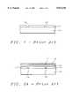
- FIG. 1shows a cross section view of an integrated circuit wafer 10 with a layer of first dielectric 12, such as an oxide, having contact holes 14 formed thereon.
- FIG. 2Ashows a cross section view of the integrated circuit wafer 10 with a layer of polysilicon 16 formed thereon. The polysilicon 16 also fills the contact holes 14 in the layer of first dielectric 12.
- a layer of HSG polysilicon 18is formed over the layer of polysilicon 16.
- Polysilicon hemispherical grainsare formed using low pressure chemical vapor deposition, LPCVD, of polysilicon at temperatures in the range of 500° to 600° C. Under these conditions the polysilicon deposits as hemispherical grains rather than a smooth film. In the process of depositing the HSG polysilicon a thin film of native oxide 11 also forms between the polysilicon layer 16 and the layer of HSG polysilicon 18.
- the layers of polysilicon 16 and HSG polysilicon 18are patterned to form a number of first capacitor plates having a top surface 21 and sidewalls 20.
- the top surface 21 of the first capacitor plateshas a number of hills and valleys due to the HSG polysilicon.
- the polysiliconis vertically anisotropically etched.
- the vertical anisotropic etchingforms a very irregular top surface 21 due to the hills and valleys of the HSG polysilicon.
- the vertical anisotropic etchingalso breaks through the native oxide on the top surface 21 of the first capacitor plates.
- the resulting irregular top surface 21increases the surface area of the first capacitor plates and the capacitance of the completed capacitor will be increased.
- the sidewalls 20 of the first capacitor platesare smooth and provide no increase in surface area.
- FIG. 1shows the layer of first dielectric 12 with contact holes 14 formed on the integrated circuit wafer 10.
- the polysilicon layer 16is patterned before the layer of HSG polysilicon is formed.
- the HSG polysiliconthen forms on the sidewalls 20 of the first capacitor plates as well as the top surface 21.
- a thin layer of native oxide 11is formed on the first capacitor plates between the polysilicon 16 and the HSG polysilicon 18.
- the polysiliconis then vertically anisotropically etched thereby forming an irregular top surface 21 and removing the HSG polysilicon from the spaces between the first capacitor plates.
- the native oxideis removed from the top surface 21 of the first capacitor plates however native oxide 11 remains on the sidewalls.
- individual hemispherical grains 19can break away from the sidewalls 20 due to the native oxide 11 and can cause shorting between adjacent first capacitor plates causing a yield loss. Residue of the hemispherical grains in the spaces between first capacitor plates can also contribute to shorting between adjacent first capacitor plates and yield loss.
- This objectiveis achieved by performing an annealing step after the hemispherical grains have been deposited and a timed vertical anisotropic etch of a part of the first dielectric layer in the spaces between first capacitor plates after the vertical anisotropic etch of the hemispherical grains.
- the phosphorous used to dope the polysilicon layerbreaks through the native oxide and prevents individual grains from becoming detached during cleaning or other processing steps.
- the timed vertical anisotropic etch of a part of the first dielectric layer in the spaces between first capacitorprevents shorting between adjacent first capacitor plates.
- FIG. 1shows a cross section view of an integrated circuit wafer after a layer of first dielectric with contact holes has been formed.
- FIGS. 2A-2Cshow cross section views of an integrated circuit wafer for a conventional method of using HSG polysilicon to form first capacitor plates having an irregular top surface and smooth sidewalls.
- FIGS. 3A-3Cshow cross section views of an integrated circuit wafer for a conventional method of using HSG polysilicon to form first capacitor plates having an irregular top surface and HSG polysilicon on the sidewalls.
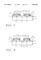
- FIG. 4shows a cross section view of an integrated circuit wafer having a layer of polysilicon formed over the layer of first dielectric having contact holes.
- FIG. 5shows a cross section view of an integrated circuit wafer after the polysilicon layer has been patterned and HSG polysilicon has been deposited.
- FIG. 6shows a cross section view of an integrated circuit wafer after the polysilicon layer has been patterned, HSG polysilicon has been deposited, and the wafer has been annealed.
- FIG. 7shows a cross section view of an integrated circuit wafer after the polysilicon layer has been patterned, HSG polysilicon has been deposited, the wafer has been annealed, and the polysilicon has been vertically anisotropically etched.
- FIG. 8shows a cross section view of an integrated circuit wafer after the polysilicon layer has been patterned, HSG polysilicon has been deposited, the wafer has been annealed, the polysilicon has been vertically anisotropically etched, and a part of the first dielectric layer has been vertically anisotropically etched thereby completing the first capacitor plates.
- FIG. 1shows a substrate 10 with a layer of first dielectric 12 formed on the substrate 10 and contact holes 14 formed in the layer of first dielectric 12.
- the substrateis a silicon integrated circuit wafer having devices, not shown, formed therein.
- the first dielectric 12is an oxide such as silicon dioxide.
- a layer of first conductor material 16is formed over the layer of first dielectric 12 filling the contact holes 14. The filled contact holes provide a connection to the first capacitor plate which will be formed from the layer of first conductor material 16.
- the first conductor material 16is phosphorous doped polysilicon.
- the layer of first conductor materialis patterned forming first capacitor plates 17 wherein each first capacitor plate 17 has sidewalls 20 and a top surface 21.
- a layer of polysilicon hemispherical grains 18, HSG polysiliconis formed over the integrated circuit wafer covering the first capacitor plates 17 and the first dielectric in the spaces between the first capacitor plates.
- the HSG polysiliconis formed using low pressure chemical vapor deposition, LPCVD, of silane, SiH 4 , at a temperature of between about 500° and 600° C. and a pressure of between about 0.01 and 0.5 Torr.
- LPCVDlow pressure chemical vapor deposition
- SiH 4silane
- a thin layer of native oxide 11having a thickness of between about 2 and 20 Angstroms is formed between the capacitor plates 17 and the layer of HSG polysilicon 18.
- the waferis then annealed at a temperature of between about 700° and 1000° C. for between about 10 and 360 minutes.
- phosphorous, or other impurities used to dope the polysiliconbreaks through the native oxide and the grains of HSG polysilicon form intimate contact with the phosphorous doped polysilicon or other conductor material forming the first capacitor plates 17.
- the phosphorous, or other doping impurities, breaking through the native oxidecomes from the doped polysilicon layer forming the first capacitor plates.
- the HSG polysiliconcan be doped providing a source of phosphorous.
- the polysilicon layer forming the first conductor plates and the HSG polysiliconcan, for example, be doped with phosphorous or arsenic.
- the HSG polysiliconis vertically anisotropically etched using dry etching methods. This etching step removes the HSG polysilicon from the spaces between the capacitor plates and etches into the top surface of the first conductor material of the first capacitor plates forming an irregular surface on the top surface 21 of the first capacitor plates 17. HSG polysilicon 18 remains firmly attached to the sidewalls 20 of the first capacitor plates 17 because of the previous annealing step.
- part of the first dielectric 12 in the spaces 22 between the first capacitor plates 17is removed using a timed etchback with vertical anisotropic etching using dry etching methods which will not remove polysilicon or other material used for the first capacitor plates.
- dry etching methodsare described in "Silicon Processing for the VLSI Era, Volume 1-Process Technology," by S. Wolf and R. N. Tauber, Lattice Press, Sunset Beach, Calif., 1986, pages 555-558.
- the waferis then cleaned using dilute hydrofluoric acid. Because of the previous annealing step the grains of HSG polysilicon 18 remain firmly attached to the sidewalls of the first capacitor plates 17.
- the timed etchback stepinsures that there will no material left between adjacent first capacitor plates 17 which could cause electrical shorting problems.
- a layer of second dielectric, not shown,is then formed over the top surface 21 and sidewalls 20 of the first capacitor plates 17. Second capacitor plates, not shown, are then formed over the first capacitor plates to complete the capacitors.
Landscapes
- Engineering & Computer Science (AREA)
- Manufacturing & Machinery (AREA)
- Semiconductor Memories (AREA)
- Semiconductor Integrated Circuits (AREA)
Abstract
Description
(1) Field of the Invention
This invention relates to the formation of high capacitance capacitors on integrated circuit wafers and more particularly to capacitor plates using etchback of polysilicon hemispherical grains.
(2) Description of the Related Art
Polysilicon hemispherical grains, HSG polysilicon, are used to increase surface area of capacitor plates used to form integrated circuit capacitors, particularly for DRAM circuits. The HSG polysilicon is formed on a conductor, usually polysilicon, used to form capacitor plates. Etchback of the HSG polysilicon using vertical anisotropic etching forms an irregular top surface of the capacitor plates. HSG polysilicon is also used on the sidewalls of the capacitor plates however adhesion of the HSG polysilicon to the sidewalls can be a problem.
U.S. Pat. No. 5,256,587 to Jun et al. describes methods of forming capacitor plates using a hemisphere particle layer having hills and valleys on a layer to be etched. The hemispherical particle layer is used on the top surface of the capacitor plates.
U.S. Pat. No. 5,254,503 to Kenny describes the use of sub-lithographic relief images to increase the surface area of the top surface of capacitor plates. Polysilicon and porous silicon can be used to form the sub-micron relief pattern.
U.S. Pat. No. 5,082,797 to Chan et al. describes the use of a texturized polysilicon structure to increase the area of capacitor plates. A polysilicon structure is subjected to a wet oxidation followed by a wet oxide etch to form the texturized polysilicon structure.
U.S. Pat. No. 5,447,878 to Park et al. describes the use of an HSG polysilicon layer of form extended surface area on both the top and the sidewalls of capacitor plates, however an anneal step after the formation of the HSG polysilicon layer and an timed oxide back etch is not described.
U.S. Pat. No. 5,492,848 to Lur et al. describes the use of silicon nodules formed on the top surface of capacitor plates to increase surface area.
U.S. Pat. No. 5,134,086 to Ahn describes exposing a first polysilicon layer, an oxide layer, and a second polysilicon layer consisting of grains to an oxide etchant. The oxide etchant penetrates the grain boundaries of the second polysilicon layer and etches the oxide layer at the grain boundaries. The etching forms an irregular surface which increases surface area. The irregular surface area is on the top surface of the capacitor plates.
U.S. Pat. No. 5,358,888 to Ahn et al. describes the use of polysilicon hemispherical grains to form an irregular surface on the top surface of capacitor plates.
A paper entitled "A CAPACITOR-OVER-BIT-LINE (COB) CELL WITH A HEMISPHERICAL-GRAIN STORAGE NODE FOR 64 Mb DRAMs", by Sakao et al., IEDM, 1990, pages 27.3.1-27.3.4 describes using etchback of HSG polysilicon to increase the surface area of capacitor plates. The use of an anneal step or a timed oxide etchback step is not described.
This invention describes the use of HSG polysilicon along with an anneal step and a timed oxide etchback step to form an irregular surface on the top and sidewalls of capacitor plates thereby increasing surface area and capacitance. The method of this invention prevents individual grains from breaking away thereby resulting in improved chip yield.
Capacitors are an important element in integrated circuit technology, particularly for DRAM technology. Capacitors, by the nature of their operation, consume valuable integrated circuit element space. As levels of integration increase the problem of space for capacitors with sufficient capacitance also increases, particularly for DRAMs. Frequently methods are employed which form irregularly shaped capacitor plates, thereby increasing the surface area of the capacitor plates, and thereby the capacitance of the capacitor, without increasing the amount of integrated circuit space required for the capacitor.
One of the methods used to increase the surface area of capacitor plates employs the use of polysilicon hemispherical grains, HSG polysilicon. FIGS. 1 and 2A-2C shows one method of increasing the surface area of capacitor plates. FIG. 1 shows a cross section view of anintegrated circuit wafer 10 with a layer of first dielectric 12, such as an oxide, havingcontact holes 14 formed thereon. FIG. 2A shows a cross section view of theintegrated circuit wafer 10 with a layer ofpolysilicon 16 formed thereon. Thepolysilicon 16 also fills thecontact holes 14 in the layer of first dielectric 12. A layer ofHSG polysilicon 18 is formed over the layer ofpolysilicon 16. Polysilicon hemispherical grains are formed using low pressure chemical vapor deposition, LPCVD, of polysilicon at temperatures in the range of 500° to 600° C. Under these conditions the polysilicon deposits as hemispherical grains rather than a smooth film. In the process of depositing the HSG polysilicon a thin film ofnative oxide 11 also forms between thepolysilicon layer 16 and the layer ofHSG polysilicon 18.
As shown in FIG. 2B the layers ofpolysilicon 16 andHSG polysilicon 18 are patterned to form a number of first capacitor plates having atop surface 21 andsidewalls 20. Thetop surface 21 of the first capacitor plates has a number of hills and valleys due to the HSG polysilicon. Next, as shown in FIG. 2C, the polysilicon is vertically anisotropically etched. The vertical anisotropic etching forms a veryirregular top surface 21 due to the hills and valleys of the HSG polysilicon. The vertical anisotropic etching also breaks through the native oxide on thetop surface 21 of the first capacitor plates. The resultingirregular top surface 21 increases the surface area of the first capacitor plates and the capacitance of the completed capacitor will be increased. However thesidewalls 20 of the first capacitor plates are smooth and provide no increase in surface area.
Another method used to increase the surface area of capacitor plates is shown in FIGS. 1 and 3A-3C. FIG. 1 shows the layer of first dielectric 12 withcontact holes 14 formed on theintegrated circuit wafer 10. In this case, as shown in FIG. 3A, thepolysilicon layer 16 is patterned before the layer of HSG polysilicon is formed. As shown in FIG. 3B the HSG polysilicon then forms on thesidewalls 20 of the first capacitor plates as well as thetop surface 21. As before a thin layer ofnative oxide 11 is formed on the first capacitor plates between thepolysilicon 16 and theHSG polysilicon 18. As shown in FIG. 3C, the polysilicon is then vertically anisotropically etched thereby forming anirregular top surface 21 and removing the HSG polysilicon from the spaces between the first capacitor plates. The native oxide is removed from thetop surface 21 of the first capacitor plates howevernative oxide 11 remains on the sidewalls. During subsequent cleaning and other processing steps individualhemispherical grains 19 can break away from thesidewalls 20 due to thenative oxide 11 and can cause shorting between adjacent first capacitor plates causing a yield loss. Residue of the hemispherical grains in the spaces between first capacitor plates can also contribute to shorting between adjacent first capacitor plates and yield loss.
It is a principle objective of this invention to provide a method of using hemispherical grains to achieve increased surface area on the top surface and sidewalls of first capacitor plates without yield loss due to individual grains breaking away or shorting between adjacent first capacitor plates.
This objective is achieved by performing an annealing step after the hemispherical grains have been deposited and a timed vertical anisotropic etch of a part of the first dielectric layer in the spaces between first capacitor plates after the vertical anisotropic etch of the hemispherical grains. During the annealing step the phosphorous used to dope the polysilicon layer breaks through the native oxide and prevents individual grains from becoming detached during cleaning or other processing steps. The timed vertical anisotropic etch of a part of the first dielectric layer in the spaces between first capacitor prevents shorting between adjacent first capacitor plates.
FIG. 1 shows a cross section view of an integrated circuit wafer after a layer of first dielectric with contact holes has been formed.
FIGS. 2A-2C show cross section views of an integrated circuit wafer for a conventional method of using HSG polysilicon to form first capacitor plates having an irregular top surface and smooth sidewalls.
FIGS. 3A-3C show cross section views of an integrated circuit wafer for a conventional method of using HSG polysilicon to form first capacitor plates having an irregular top surface and HSG polysilicon on the sidewalls.
FIG. 4 shows a cross section view of an integrated circuit wafer having a layer of polysilicon formed over the layer of first dielectric having contact holes.
FIG. 5 shows a cross section view of an integrated circuit wafer after the polysilicon layer has been patterned and HSG polysilicon has been deposited.
FIG. 6 shows a cross section view of an integrated circuit wafer after the polysilicon layer has been patterned, HSG polysilicon has been deposited, and the wafer has been annealed.
FIG. 7 shows a cross section view of an integrated circuit wafer after the polysilicon layer has been patterned, HSG polysilicon has been deposited, the wafer has been annealed, and the polysilicon has been vertically anisotropically etched.
FIG. 8 shows a cross section view of an integrated circuit wafer after the polysilicon layer has been patterned, HSG polysilicon has been deposited, the wafer has been annealed, the polysilicon has been vertically anisotropically etched, and a part of the first dielectric layer has been vertically anisotropically etched thereby completing the first capacitor plates.
Refer now to FIGS. 1 and 4-8 for a description of the preferred embodiments of the method of forming capacitor plates of this invention. FIG. 1 shows asubstrate 10 with a layer of first dielectric 12 formed on thesubstrate 10 and contact holes 14 formed in the layer offirst dielectric 12. In this example the substrate is a silicon integrated circuit wafer having devices, not shown, formed therein. In this example thefirst dielectric 12 is an oxide such as silicon dioxide. Next, as shown in FIG. 4, a layer offirst conductor material 16 is formed over the layer of first dielectric 12 filling the contact holes 14. The filled contact holes provide a connection to the first capacitor plate which will be formed from the layer offirst conductor material 16. In this example thefirst conductor material 16 is phosphorous doped polysilicon. Next as shown in FIG. 5 the layer of first conductor material is patterned formingfirst capacitor plates 17 wherein eachfirst capacitor plate 17 has sidewalls 20 and atop surface 21.
Next, as shown in FIG. 5, a layer of polysiliconhemispherical grains 18, HSG polysilicon, is formed over the integrated circuit wafer covering thefirst capacitor plates 17 and the first dielectric in the spaces between the first capacitor plates. In this example the HSG polysilicon is formed using low pressure chemical vapor deposition, LPCVD, of silane, SiH4, at a temperature of between about 500° and 600° C. and a pressure of between about 0.01 and 0.5 Torr. During the formation of the layer of HSG polysilicon a thin layer ofnative oxide 11, having a thickness of between about 2 and 20 Angstroms is formed between thecapacitor plates 17 and the layer ofHSG polysilicon 18.
Next, as shown in FIG. 6, the wafer is then annealed at a temperature of between about 700° and 1000° C. for between about 10 and 360 minutes. During this anneal step phosphorous, or other impurities used to dope the polysilicon, breaks through the native oxide and the grains of HSG polysilicon form intimate contact with the phosphorous doped polysilicon or other conductor material forming thefirst capacitor plates 17. The phosphorous, or other doping impurities, breaking through the native oxide comes from the doped polysilicon layer forming the first capacitor plates. If other conductor materials are used the HSG polysilicon can be doped providing a source of phosphorous. The polysilicon layer forming the first conductor plates and the HSG polysilicon can, for example, be doped with phosphorous or arsenic.
Next, as shown in FIG. 7, the HSG polysilicon is vertically anisotropically etched using dry etching methods. This etching step removes the HSG polysilicon from the spaces between the capacitor plates and etches into the top surface of the first conductor material of the first capacitor plates forming an irregular surface on thetop surface 21 of thefirst capacitor plates 17.HSG polysilicon 18 remains firmly attached to thesidewalls 20 of thefirst capacitor plates 17 because of the previous annealing step.
Next, as shown in FIG. 8, part of thefirst dielectric 12 in thespaces 22 between thefirst capacitor plates 17 is removed using a timed etchback with vertical anisotropic etching using dry etching methods which will not remove polysilicon or other material used for the first capacitor plates. Examples of dry etching methods are described in "Silicon Processing for the VLSI Era, Volume 1-Process Technology," by S. Wolf and R. N. Tauber, Lattice Press, Sunset Beach, Calif., 1986, pages 555-558. The wafer is then cleaned using dilute hydrofluoric acid. Because of the previous annealing step the grains ofHSG polysilicon 18 remain firmly attached to the sidewalls of thefirst capacitor plates 17. The timed etchback step insures that there will no material left between adjacentfirst capacitor plates 17 which could cause electrical shorting problems. A layer of second dielectric, not shown, is then formed over thetop surface 21 and sidewalls 20 of thefirst capacitor plates 17. Second capacitor plates, not shown, are then formed over the first capacitor plates to complete the capacitors.
While the invention has been particularly shown and described with reference to the preferred embodiments thereof, it will be understood by those skilled in the art that various changes in form and details may be made without departing from the spirit and scope of the invention.
Claims (20)
1. A method of forming capacitors, comprising the steps of:
providing a substrate;
forming a layer of first dielectric on said substrate;
forming contact holes in said layer of first dielectric;
forming a layer of first conductor material on said layer of first dielectric thereby filling said contact holes in said layer of first dielectric;
patterning said layer of first conductor material thereby forming a number of first capacitor plates, wherein each said first capacitor plate has a top surface and sidewalls, and spaces between said first capacitor plates wherein those portions of said layer of first dielectric in said spaces are exposed;
forming a layer of polysilicon hemispherical grains on said top surface and sidewalls of each said first capacitor plate and said portions of said layer of first dielectric in said spaces between said first capacitor plates;
annealing said substrate after forming said layer of hemispherical grains;
anisotropically etching said layer of hemispherical grains and said first capacitor plates after annealing said substrate thereby forming an irregular top surface on each said first capacitor plate and removing those portions of said layer of hemispherical grains in said spaces between said first capacitor plates;
anisotropically etching said portions of said layer of first dielectric in said spaces between said first capacitor plates using said first capacitor plates as a mask;
cleaning said substrate after anisotropically etching said portions of said layer of first dielectric in said spaces between said first capacitor plates;
forming a second dielectric on said irregular top surface and said sidewalls of each said first capacitor plate; and
forming a second capacitor plate over said second dielectric formed on said irregular top surface and said sidewalls of each said first capacitor plate.
2. The method of claim 1 wherein said first conductor material is doped polysilicon.
3. The method of claim 2 wherein said doped polysilicon is polysilicon doped with phosphorous or arsenic.
4. The method of claim 1 wherein said first dielectric is an oxide or silicon nitride.
5. The method of claim 1 wherein said annealing said substrate is carried out at a temperature of between about 700° and 1000° C.
6. The method of claim 1 wherein said polysilicon hemispherical grains are formed by means of low pressure chemical vapor deposition using silane at a temperature of between about 500° and 600° C. and a pressure of between about 0.01 and 0.5 Torr.
7. The method of claim 1 wherein said polysilicon hemispherical grains are formed of phosphorous doped polysilicon or arsenic doped polysilicon.
8. The method of claim 1 wherein cleaning said substrate is accomplished using dilute hydrofluoric acid.
9. The method of claim 1 wherein said anisotropically etching said layer of hemispherical grains consists of vertically anisotropically etching said layer of hemispherical grains.
10. The method of claim 1 wherein said anisotropically etching said portions of said layer of first dielectric in said spaces between said first capacitor plates consists of vertically anisotropically etching said portions of said layer of first dielectric in said spaces between said first capacitor plates.
11. The method of claim 1 wherein said substrate is a silicon integrated circuit wafer having devices formed therein.
12. A method of forming capacitors, comprising the steps of:
providing an integrated circuit wafer having devices formed therein;
forming a layer of first dielectric on said substrate;
forming contact holes in said layer of first dielectric;
forming a layer of doped polysilicon on said layer of first dielectric thereby filling said contact holes in said layer of first dielectric;
patterning said layer of doped polysilicon thereby forming a number of first capacitor plates, wherein each said first capacitor plate has a top surface and sidewalls, and spaces between said first capacitor plates wherein those portions of said layer of first dielectric in said spaces are exposed;
forming a layer of polysilicon hemispherical grains on said top surface and sidewalls of each said first capacitor plate and said portions of said layer of first dielectric in said spaces between said first capacitor plates;
annealing said integrated circuit wafer after forming said layer of polysilicon hemispherical grains;
anisotropically etching said layer of polysilicon hemispherical grains and said capacitor plates after annealing said integrated circuit wafer thereby forming an irregular top surface on each said first capacitor plate and removing those portions of said layer of polysilicon hemispherical grains in said spaces between said first capacitor plates;
anisotropically etching said portions of said layer of first dielectric in said spaces between said first capacitor plates using said first capacitor plates as a mask;
cleaning said integrated circuit wafer after anisotropically etching said portions of said layer of first dielectric in said spaces between said first capacitor plates;
forming a second dielectric on said irregular top surface and said sidewalls of each said first capacitor plate; and
forming a second capacitor plate over said second dielectric formed on said irregular top surface and said sidewalls of each said first capacitor plate.
13. The method of claim 12 wherein said first dielectric is an oxide or silicon nitride.
14. The method of claim 12 wherein said annealing said integrated circuit wafer is carried out at a temperature of between about 700° and 1000° C.
15. The method of claim 12 wherein said polysilicon hemispherical grains are formed by means of low pressure chemical vapor deposition using silane at a temperature of between about 500° and 600° C. and a pressure of between about 0.01 and 0.5 Torr.
16. The method of claim 12 wherein cleaning said integrated circuit wafer is accomplished using dilute hydrofluoric acid.
17. The method of claim 12 wherein said doped polysilicon is doped with phosphorous or arsenic.
18. The method of claim 12 wherein said polysilicon hemispherical grains are doped with phosphorous or arsenic.
19. The method of claim 12 wherein said anisotropically etching said layer of polysilicon hemispherical grains consists of vertically anisotropically etching said layer of polysilicon hemispherical grains.
20. The method of claim 12 wherein said anisotropically etching said portions of said layer of first dielectric in said spaces between said first capacitor plates consists of vertically anisotropically etching said portions of said layer of first dielectric in said spaces between said first capacitor plates.
Priority Applications (1)
| Application Number | Priority Date | Filing Date | Title |
|---|---|---|---|
| US08/880,953US5874336A (en) | 1997-06-23 | 1997-06-23 | Method to improve yield for capacitors formed using etchback of polysilicon hemispherical grains |
Applications Claiming Priority (1)
| Application Number | Priority Date | Filing Date | Title |
|---|---|---|---|
| US08/880,953US5874336A (en) | 1997-06-23 | 1997-06-23 | Method to improve yield for capacitors formed using etchback of polysilicon hemispherical grains |
Publications (1)
| Publication Number | Publication Date |
|---|---|
| US5874336Atrue US5874336A (en) | 1999-02-23 |
Family
ID=25377473
Family Applications (1)
| Application Number | Title | Priority Date | Filing Date |
|---|---|---|---|
| US08/880,953Expired - LifetimeUS5874336A (en) | 1997-06-23 | 1997-06-23 | Method to improve yield for capacitors formed using etchback of polysilicon hemispherical grains |
Country Status (1)
| Country | Link |
|---|---|
| US (1) | US5874336A (en) |
Cited By (11)
| Publication number | Priority date | Publication date | Assignee | Title |
|---|---|---|---|---|
| US5937307A (en)* | 1997-12-19 | 1999-08-10 | United Microelectronics Corp. | Process for fabricating DRAM capacitor |
| US6043132A (en)* | 1997-09-26 | 2000-03-28 | Samsung Electronics Co., Ltd. | Method for forming HSG silicon film of semiconductor device |
| US6090664A (en)* | 1998-07-22 | 2000-07-18 | Worldwide Semiconductor Manufacturing Corporation | Method for making a stacked DRAM capacitor |
| US6121109A (en)* | 1998-10-03 | 2000-09-19 | United Semiconductor Corp. | Method of forming hemispherical grain polysilicon over lower electrode capacitor |
| US6153465A (en)* | 1997-12-01 | 2000-11-28 | United Microelectronics Corp. | Method of fabricating a capacitor of dynamic random access memory |
| US6177309B1 (en) | 1998-06-15 | 2001-01-23 | Samsung Electronics Co., Ltd. | Methods of forming integrated circuit capacitors having merged annular storage electrodes therein |
| US6218260B1 (en) | 1997-04-22 | 2001-04-17 | Samsung Electronics Co., Ltd. | Methods of forming integrated circuit capacitors having improved electrode and dielectric layer characteristics and capacitors formed thereby |
| US6228709B1 (en)* | 1997-11-27 | 2001-05-08 | United Microelectronics Corp. | Method of fabricating hemispherical grain electrode |
| US6238968B1 (en) | 1999-03-18 | 2001-05-29 | Samsung Electronics Co., Ltd. | Methods of forming integrated circuit capacitors having protected layers of HSG silicon therein |
| US6385020B1 (en) | 1999-01-20 | 2002-05-07 | Samsung Electronics Co., Ltd. | Methods of forming HSG capacitors from nonuniformly doped amorphous silicon layers and HSG capacitors formed thereby |
| US20030075751A1 (en)* | 1998-09-03 | 2003-04-24 | Kao David Y. | Gapped-plate capacitor |
Citations (8)
| Publication number | Priority date | Publication date | Assignee | Title |
|---|---|---|---|---|
| US5082797A (en)* | 1991-01-22 | 1992-01-21 | Micron Technology, Inc. | Method of making stacked textured container capacitor |
| US5134086A (en)* | 1991-03-20 | 1992-07-28 | Samsung Electronics Co., Ltd. | Method for manufacturing capacitor of highly integrated semiconductor memory device |
| US5254503A (en)* | 1992-06-02 | 1993-10-19 | International Business Machines Corporation | Process of making and using micro mask |
| US5256587A (en)* | 1991-03-20 | 1993-10-26 | Goldstar Electron Co., Ltd. | Methods of patterning and manufacturing semiconductor devices |
| US5358888A (en)* | 1991-12-18 | 1994-10-25 | Samsung Electronics Co., Ltd. | Method for manufacturing a capacitor of an integrated semiconductor device having increased surface area |
| US5447878A (en)* | 1992-09-19 | 1995-09-05 | Samsung Electronics Co., Ltd. | Method for manufacturing a semiconductor memory device having a capacitor with increased effective area |
| US5492848A (en)* | 1994-03-18 | 1996-02-20 | United Microelectronics Corp. | Stacked capacitor process using silicon nodules |
| US5622889A (en)* | 1995-01-26 | 1997-04-22 | Samsung Electronics Co., Ltd. | High capacitance capacitor manufacturing method |
- 1997
- 1997-06-23USUS08/880,953patent/US5874336A/ennot_activeExpired - Lifetime
Patent Citations (8)
| Publication number | Priority date | Publication date | Assignee | Title |
|---|---|---|---|---|
| US5082797A (en)* | 1991-01-22 | 1992-01-21 | Micron Technology, Inc. | Method of making stacked textured container capacitor |
| US5134086A (en)* | 1991-03-20 | 1992-07-28 | Samsung Electronics Co., Ltd. | Method for manufacturing capacitor of highly integrated semiconductor memory device |
| US5256587A (en)* | 1991-03-20 | 1993-10-26 | Goldstar Electron Co., Ltd. | Methods of patterning and manufacturing semiconductor devices |
| US5358888A (en)* | 1991-12-18 | 1994-10-25 | Samsung Electronics Co., Ltd. | Method for manufacturing a capacitor of an integrated semiconductor device having increased surface area |
| US5254503A (en)* | 1992-06-02 | 1993-10-19 | International Business Machines Corporation | Process of making and using micro mask |
| US5447878A (en)* | 1992-09-19 | 1995-09-05 | Samsung Electronics Co., Ltd. | Method for manufacturing a semiconductor memory device having a capacitor with increased effective area |
| US5492848A (en)* | 1994-03-18 | 1996-02-20 | United Microelectronics Corp. | Stacked capacitor process using silicon nodules |
| US5622889A (en)* | 1995-01-26 | 1997-04-22 | Samsung Electronics Co., Ltd. | High capacitance capacitor manufacturing method |
Non-Patent Citations (2)
| Title |
|---|
| "A Capacitor-Over-Bit-Lhe (COB) Cell with a Hemispherical Grain Storage Node for 64 MbDRAMS" by Sakao et al, IEDM, 1990, pp. 27.31-27.34. |
| A Capacitor Over Bit Lhe (COB) Cell with a Hemispherical Grain Storage Node for 64 MbDRAMS by Sakao et al, IEDM, 1990, pp. 27.31 27.34.* |
Cited By (20)
| Publication number | Priority date | Publication date | Assignee | Title |
|---|---|---|---|---|
| US6624069B2 (en) | 1997-04-22 | 2003-09-23 | Samsung Electronics Co., Ltd. | Methods of forming integrated circuit capacitors having doped HSG electrodes |
| US6876029B2 (en) | 1997-04-22 | 2005-04-05 | Samsung Electronics Co., Ltd. | Integrated circuit capacitors having doped HSG electrodes |
| US20040033662A1 (en)* | 1997-04-22 | 2004-02-19 | Seung-Hwan Lee | Integrated circuit capacitors having doped HSG electrodes |
| US6218260B1 (en) | 1997-04-22 | 2001-04-17 | Samsung Electronics Co., Ltd. | Methods of forming integrated circuit capacitors having improved electrode and dielectric layer characteristics and capacitors formed thereby |
| US6043132A (en)* | 1997-09-26 | 2000-03-28 | Samsung Electronics Co., Ltd. | Method for forming HSG silicon film of semiconductor device |
| US6228709B1 (en)* | 1997-11-27 | 2001-05-08 | United Microelectronics Corp. | Method of fabricating hemispherical grain electrode |
| US6153465A (en)* | 1997-12-01 | 2000-11-28 | United Microelectronics Corp. | Method of fabricating a capacitor of dynamic random access memory |
| US5937307A (en)* | 1997-12-19 | 1999-08-10 | United Microelectronics Corp. | Process for fabricating DRAM capacitor |
| US6177309B1 (en) | 1998-06-15 | 2001-01-23 | Samsung Electronics Co., Ltd. | Methods of forming integrated circuit capacitors having merged annular storage electrodes therein |
| US6090664A (en)* | 1998-07-22 | 2000-07-18 | Worldwide Semiconductor Manufacturing Corporation | Method for making a stacked DRAM capacitor |
| US20030075751A1 (en)* | 1998-09-03 | 2003-04-24 | Kao David Y. | Gapped-plate capacitor |
| US6774421B2 (en)* | 1998-09-03 | 2004-08-10 | Micron Technology, Inc. | Gapped-plate capacitor |
| US20040264104A1 (en)* | 1998-09-03 | 2004-12-30 | Kao David Y. | Gapped-plate capacitor |
| US20050121740A1 (en)* | 1998-09-03 | 2005-06-09 | Kao David Y. | Gapped-plate capacitor |
| US6958901B2 (en) | 1998-09-03 | 2005-10-25 | Micron Technology, Inc. | Gapped-plate capacitor |
| US7151659B2 (en) | 1998-09-03 | 2006-12-19 | Micron Technology, Inc. | Gapped-plate capacitor |
| US20070058325A1 (en)* | 1998-09-03 | 2007-03-15 | Micron Technology, Inc. | Gapped-plate capacitor |
| US6121109A (en)* | 1998-10-03 | 2000-09-19 | United Semiconductor Corp. | Method of forming hemispherical grain polysilicon over lower electrode capacitor |
| US6385020B1 (en) | 1999-01-20 | 2002-05-07 | Samsung Electronics Co., Ltd. | Methods of forming HSG capacitors from nonuniformly doped amorphous silicon layers and HSG capacitors formed thereby |
| US6238968B1 (en) | 1999-03-18 | 2001-05-29 | Samsung Electronics Co., Ltd. | Methods of forming integrated circuit capacitors having protected layers of HSG silicon therein |
Similar Documents
| Publication | Publication Date | Title |
|---|---|---|
| US7179706B2 (en) | Permeable capacitor electrode | |
| US6261899B1 (en) | Semiconductor processing methods of forming integrated circuitry memory devices, methods of forming capacitor containers, methods of making electrical connection to circuit nodes and related integrated circuitry | |
| US5478769A (en) | Process for fabricating a stashed capacitor in a semiconductor device | |
| US6025223A (en) | Methods of forming high dielectric capacitors | |
| KR0165496B1 (en) | Capacitor Manufacturing Method for Highly Integrated Semiconductor Devices | |
| US5858838A (en) | Method for increasing DRAM capacitance via use of a roughened surface bottom capacitor plate | |
| US5656529A (en) | Method for manufacturing highly-integrated capacitor | |
| US6027970A (en) | Method of increasing capacitance of memory cells incorporating hemispherical grained silicon | |
| US6331720B1 (en) | Electrically conductive structure | |
| JP3640763B2 (en) | Manufacturing method of capacitor of semiconductor memory device | |
| US5874336A (en) | Method to improve yield for capacitors formed using etchback of polysilicon hemispherical grains | |
| US5723373A (en) | Method of making porous-Si capacitors for high density drams cell | |
| US6395615B2 (en) | Selective silicon formation for semiconductor devices | |
| JP3233051B2 (en) | Method for manufacturing semiconductor device | |
| US5759895A (en) | Method of fabricating a capacitor storage node having a rugged-fin surface | |
| US5907774A (en) | Corrugated post capacitor and method of fabricating using selective silicon deposition | |
| US5770510A (en) | Method for manufacturing a capacitor using non-conformal dielectric | |
| US6127221A (en) | In situ, one step, formation of selective hemispherical grain silicon layer, and a nitride-oxide dielectric capacitor layer, for a DRAM application | |
| US20010044182A1 (en) | Semiconductor device having hsg polycrystalline silicon layer | |
| US5679596A (en) | Spot deposited polysilicon for the fabrication of high capacitance, DRAM devices | |
| JP2001210806A (en) | Method of forming lower electrode using electroplating method | |
| US5691227A (en) | Method for forming charge storage electrodes of semiconductor device | |
| US6245633B1 (en) | Fabrication method for a double-side double-crown stacked capacitor | |
| CN1128471C (en) | Method for forming capacitors using die etch back of polysilicon hemispheres | |
| US5973350A (en) | Stacked capacitor structure for high density DRAM cells |
Legal Events
| Date | Code | Title | Description |
|---|---|---|---|
| AS | Assignment | Owner name:VANGUARD INTERNATIONAL SEMICONDUCTOR CORPORATION, Free format text:ASSIGNMENT OF ASSIGNORS INTEREST;ASSIGNOR:CHERNG, GEORGE MENG-JAW;REEL/FRAME:008671/0080 Effective date:19970605 | |
| STCF | Information on status: patent grant | Free format text:PATENTED CASE | |
| FPAY | Fee payment | Year of fee payment:4 | |
| FPAY | Fee payment | Year of fee payment:8 | |
| FPAY | Fee payment | Year of fee payment:12 | |
| FEPP | Fee payment procedure | Free format text:PAYOR NUMBER ASSIGNED (ORIGINAL EVENT CODE: ASPN); ENTITY STATUS OF PATENT OWNER: LARGE ENTITY Free format text:PAYER NUMBER DE-ASSIGNED (ORIGINAL EVENT CODE: RMPN); ENTITY STATUS OF PATENT OWNER: LARGE ENTITY | |
| AS | Assignment | Owner name:TAIWAN SEMICONDUCTOR MANUFACTURING CO., LTD., TAIW Free format text:ASSIGNMENT OF ASSIGNORS INTEREST;ASSIGNOR:VANGUARD INTERNATIONAL SEMICONDUCTOR CORPORATION;REEL/FRAME:025645/0432 Effective date:20101026 |