US5872994A - Flash memory incorporating microcomputer having on-board writing function - Google Patents
Flash memory incorporating microcomputer having on-board writing functionDownload PDFInfo
- Publication number
- US5872994A US5872994AUS08/745,828US74582896AUS5872994AUS 5872994 AUS5872994 AUS 5872994AUS 74582896 AUS74582896 AUS 74582896AUS 5872994 AUS5872994 AUS 5872994A
- Authority
- US
- United States
- Prior art keywords
- register
- circuit
- clock signal
- microcomputer
- value
- Prior art date
- Legal status (The legal status is an assumption and is not a legal conclusion. Google has not performed a legal analysis and makes no representation as to the accuracy of the status listed.)
- Expired - Lifetime
Links
Images


Classifications
- G—PHYSICS
- G06—COMPUTING OR CALCULATING; COUNTING
- G06F—ELECTRIC DIGITAL DATA PROCESSING
- G06F11/00—Error detection; Error correction; Monitoring
- G06F11/07—Responding to the occurrence of a fault, e.g. fault tolerance
- G06F11/14—Error detection or correction of the data by redundancy in operation
- G06F11/1402—Saving, restoring, recovering or retrying
- G06F11/1415—Saving, restoring, recovering or retrying at system level
- G06F11/1433—Saving, restoring, recovering or retrying at system level during software upgrading
- G—PHYSICS
- G06—COMPUTING OR CALCULATING; COUNTING
- G06F—ELECTRIC DIGITAL DATA PROCESSING
- G06F12/00—Accessing, addressing or allocating within memory systems or architectures
- G06F12/02—Addressing or allocation; Relocation
- G06F12/08—Addressing or allocation; Relocation in hierarchically structured memory systems, e.g. virtual memory systems
- G—PHYSICS
- G06—COMPUTING OR CALCULATING; COUNTING
- G06F—ELECTRIC DIGITAL DATA PROCESSING
- G06F11/00—Error detection; Error correction; Monitoring
- G06F11/07—Responding to the occurrence of a fault, e.g. fault tolerance
- G06F11/14—Error detection or correction of the data by redundancy in operation
- G—PHYSICS
- G06—COMPUTING OR CALCULATING; COUNTING
- G06F—ELECTRIC DIGITAL DATA PROCESSING
- G06F11/00—Error detection; Error correction; Monitoring
- G06F11/22—Detection or location of defective computer hardware by testing during standby operation or during idle time, e.g. start-up testing
- G—PHYSICS
- G06—COMPUTING OR CALCULATING; COUNTING
- G06F—ELECTRIC DIGITAL DATA PROCESSING
- G06F15/00—Digital computers in general; Data processing equipment in general
- G06F15/76—Architectures of general purpose stored program computers
- G06F15/78—Architectures of general purpose stored program computers comprising a single central processing unit
Definitions
- the present inventionrelates to a flash memory incorporating microcomputer, and more partucilarly, to the testing of the microcomputer.
- Microcomputershave been broadly incorporated into cameras, audio-visual apparatus, automobiles and the like.
- a control program for operating a microcomputeris stored in a read-only memory (ROM).
- ROMread-only memory
- the mask ROMhas been replaced by an erasable and programmable ROM (EPROM), an electrically-erasable programmable ROM (EEPROM), or a flash EEPROM which is called a flash memory.
- a prior art flash memory incorporating microcomputerincludes input/output ports, a serial ccommunication interface, a mode control unit for setting various operation modes, a flash EEROM for storing a control program, a random access memory (RAM) for storing temporary data, a read-only memory (ROM) for storing a writing program for writing the control program into the flash EEPROM, a central processing unit (CPU) and internal buses for connecting these elements to each other (see JP-A-5-266219). This will be explained later in detail.
- the ROMis active only for an on-board writing operation mode; in other words, the ROM is inactive for the other operation modes. Therefore, when the ROM is incorporated into one chip of the microcomputer, the chip area thereof is increased, thus reducing the manufacturing yield.
- serial communication interfaceis fixed to one of the types of communication systems, an upper system is limited.
- control programsince the control program is temporarily stored in the RAM or a buffer of the CPU, the time required for a writing operation of the control program is long.
- the frequency of a clock signalis changed by an upper system or the type of the serial communication interface, the time period of a writing operation and the time period of a flash erasing operation are also changed.
- Another objectis to reduce the chip area of a flash memory incorporating microcomputer.
- a further objectis to match a flash memory incorporating microcomputer with various kinds of upper systems.
- a still further objectis to increase the operation speed of an on-board writing operation mode of a flash memory incorporating microcomputer.
- a further objectis to make the writing time period and the flash erasing time period of a flash memory almost constant even when the frequency of a clock signal is changed by upper systems or the like.
- a switching circuitis connected between the ROM and the internal buses and between the input/output port and the internal buses.
- the mode control unitoperates the switching circuit in an emulation test mode so that the ROM is deactivated and the input/output port is activated.
- the CPUreads the program from the serial communication interface and writes the program into the flash memory in accordance with a writing program from the input/output port.
- a writing program for writing a program into the flash memoryis incorporated into the RAM.
- the ROM for storing the writing programis unnecessary, so that the chip area of the microcomputer can be reduced.
- the serial communication interfaceincludes a plurality of kinds of serial communication interface units and a selector for selecting one of the serial communication interface units.
- the microcomputercan respond to various kinds of upper systems.
- the read speed of a programis detected by a data reception time detector.
- the CPUtemporarily stores the program in the RAM or a buffer of the CPU before writing the program into the flash memory.
- the CPUdirectly writes the program into the flash memory.
- a value of a register for defining a writing operation time period or a flash erasing operation time periodis variable.
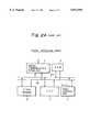
- FIG. 1is a block circuit diagram illustrating a prior art flash memory incorporating microcomputer
- FIGS. 2A, 2B, 2C and 2Dare block circuit diagrams for showing the operations of the microcomputer of FIG. 1;
- FIG. 3is a detailed circuit diagram of the flash EEPROM of FIG. 1;
- FIG. 4is a detailed circuit diagram of the control circuit of FIG. 3;
- FIG. 5is a block circuit diagram illustrating a first embodiment of the flash memory incorporating microcomputer according to the present invention
- FIG. 6is a block circuit diagram for showing the operation of the microcomputer of FIG. 5;
- FIG. 7is a block circuit diagram illustrating a second embodiment of the flash memory incorporating microcomputer according to the present invention.
- FIG. 8is a block circuit diagram for showing the operation of the microcomputer of FIG. 7;
- FIG. 9is a block circuit diagram illustrating a third embodiment of the flash memory incorporating microcomputer according to the present invention.
- FIG. 10is a block circuit diagram illustrating a fourth embodiment of the flash memory incorporating microcomputer according to the present invention.
- FIG. 11Ais a circuit diagram illustrating a fifth embodiment of the flash memory incorporating microcomputer according to the present invention.
- FIGS. 11B, 11C and 11Dare circuit diagrams of modifications of the circuit of FIG. 11A.
- FIGS. 1 2A through 2D, 3 and 4see: JP-A-5-266219).
- FIG. 1provided between internal buses such as an address bus AB, a data bus DB and a control bus (not shown) and external circuits (not shown) are input/output ports 1a and 1b and a serial communication interface 2 for receiving an address signal, a data signal and a control signal and transmitting them.
- internal busessuch as an address bus AB, a data bus DB and a control bus (not shown) and external circuits (not shown) are input/output ports 1a and 1b and a serial communication interface 2 for receiving an address signal, a data signal and a control signal and transmitting them.
- a mode control unit 3receives various mode signals from the data bus DB to set various operation modes in each section of the microcomputer of FIG. 1.
- a flash EEPROM 4is connected to the address bus AB, the data bus DB and the control bus. That is, in a write mode, a control program is written from the data bus DB into the flash EEPROM 4 whose address is designated by the address signal at the address bus AB. Also, in a read mode, the control program is read to the data bus DB from the flash EEPROM 4 whose address is designated by the address signal at the address bus AB.
- a RAM 5is connected to the address bus AB, the data bus DB and the control bus. That is, in a write mode, data is written from the data bus DB into the RAM 5 whose address is designated by the address signal at the address bus AB. Also, in a read mode, data is read to the data bus DB from the RAM 5 whose address is designated by the address signal at the address bus AB.
- a ROM 6stores a writing program for writing the control program into the flash EEPROM 4.
- a CPU 7controls the input/output ports 1a and 1b, the serial communication interface 2, the flash EEPROM 4, the RAM 5 and the ROM 6 in accordance with operation modes set by the mode control unit 3.
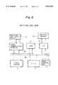
- FIGS. 2A, 2B, 2C and 2DThe operation of the microcomputer of FIG. 1 is explained next with reference to FIGS. 2A, 2B, 2C and 2D, in which only the operated blocks are extracted from FIG. 1.
- FIG. 2AA usual operation is illustrated in FIG. 2A.
- the mode control unit 3recognizes a usual operation mode by the data signal at the data bus DB supplied from the input/output port 1a (not shown in FIG. 2A, but shown in FIG. 1) or the like.
- the mode control unit 3connects the serial communication interface 2, the flash EEPROM 4, the RAM 5 and the CPU 7 to the address bus AB, the data bus DB and the control bus.
- the input/output port 1a or 1bcan be connected to the address bus AB, the data bus DB and the control bus simultaneously with the serial communication interface 2 or instead of the serial communication interface 2.
- the CPU 7reads the control program from the flash EEPROM 4 to control the serial communication interface 2, the flash EEPROM 4 and the RAM 5. For example, the CPU 7 performs a predetermined operation upon signals supplied via the serial communication interface 2 from the external circuit (not shown) and returns resulting signals to the external circuit. Also, the CPU 7 reads data from the RAM 5 to perform a predetermined operation upon the data, and writes resulting data into the RAM 5.
- FIG. 2BAn on-board writing operation mode is illustrated in FIG. 2B.
- a control program source 11is connected via an adapter (not shown) to the serial communication interface; however, such a control program source 11 can be connected to the input/output port 1a or 1b.
- the mode control unit 3recognizes an on-board writing operation mode by the data signal at the data bus DB supplied from the input/output port 1a (not shown in FIG. 2A, but shown in FIG. 1) or the like, the mode control unit 3 connects the serial communication interface 2, the flash EEPROM 4, the RAM 5 and the CPU 7 to the address bus AB, the data bus DB and the control bus.
- the CPU 7reads the control program via the serial communication interface 2 from the control program source 11 in accordance with the writing program stored in the ROM 6, and temporarily stores the control program into the RAM 5. Then, the control program is written into the flash EEPROM 4 at a predetermined timing. Note that the control program can be temporarily stored in a buffer 7a of the CPU 7 instead of the RAM 5.
- a CPU testing modeis illustrated in FIG. 2C.
- a test program memory 12is connected to the input/output port 1a; however, such a test program memory 12 can be connected to the serial communication interface 12.
- the mode control unit 3recognizes a CPU testing mode by the data signal at the data bus DB supplied from the input/output port 1a, the mode control unit 3 connects the input/output port 1a, the RAM 5 and the CPU 7 to the address bus AB, the data bus DB and the control bus. That is, the flash EEPROM 4 is separated from the internal buses.
- the CPU 7reads a test program from the test program memory 12, so as to carry out various operations in accordance with the test program. For example, temporary data is stored in the RAM 5, and result data is outputted via the input/output port 1a to the test program memory 12 or via the intput/output port 1b (not shown in FIG. 2C, but shown in FIG. 1).
- an LSI testerinstead of the test program memory 12 can be connected to the input/output port 1a.
- test patternsare generated from the LSI tester, to perform a test upon the microcomputer.
- FIG. 2DA flash EEPROM testing mode is illustrated in FIG. 2D.
- a flash EEPROM 4is connected to the address bus AB, the data bus DB and the control bus. That is, the CPU 7 is separated from the internal buses.
- the flash EEPROM tester 13performs a writing operation, a writing verification operation, a flash erasing operation and an erasing verification operation upon the flash EEPROM 4.
- a testing time for the flash EEPROM 4 by the flash EEPROM tester 13can be reduced as compared with that by the CPU 7.
- serial communication interface 2There are various types of the serial communication interface 2.
- Oneis a clock synchronous three-wire communication interface using three signal lines for a clock signal, a transmitting data signal and a receiving data signal.
- Anotheris an asynchronous two-wire communicaiton interface (UART) using two signal lines for a transmitting data signal and a receiving data signal each having a start pulse and a stop pulse.
- Still anotheris a synchroonous IIC bus communication interface using two signal lines for a clock signal and a transmitting/receiving data signal.
- One of the types of serial communication interfacesis adopted in accordance with the scale of the serial communication interface 2, the characteristics such as operating speed, a characteristic of resistance to environment such as noise, the number of signals, the kind of upper system including the microcomputer, the ratio of chip area of the serial communication interface 2 to that of the microcomputer, the matching of the upper system and the like.
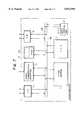
- FIG. 3which is a detailed circuit diagram of the flash EEPROM of FIG. 1, a plurality of word lines WL0, WL1, . . . and a plurality of bit lines BL0, BL1, . . . are provided.
- Reference numeral 41designates a memory cell array formed by memory cells M00, M01, . . . each having a source, a drain connected to one of the bit lines BL0, BL1, . . . a floating gate, and a control gate connected to one of the word lines WL0, WL1, . . . .
- a row decoder 42selects one of the word lines WL0, WL1, . . . .
- a column selection circuit 43 and a column decoder 44selects one of the bit lines BL0, BL1, . . . . That is, the column selection circuit 43 is formed by column selection transistors Q C0 , Q C1 , . . . each connected between one of the bit lines BL0, BL1, . . . and a digit line DL.
- One of the column selection transistors Q C0 , Q C1 , . . .is selected and turned ON by the column decoder 44.
- the row decoder 42 and the column decoder 44receive address signals from the address bus AB.
- a write amplifier 45receives data from the data bus DB and transmits it to the digit line DL.
- a sense amplifier 46senses data at the digit line DL and transmits it to the data bus DB.
- Voltages applied to the row decoder 42, the column decoder 44, the write amplifier 45 and the sources of the memory cells M00, M01, . . .are controlled by a control circuit 47 as well as voltage generating circuit 48, 49 and 50.
- the control circuit 47receives a write enable signal WE and an erase signal ER from a control bus CB which is not shown in FIG. 1.
- the control circuit 47when the control circuit 47 receives the write enable signal WE, the control circuit 47 generates a control signal WE1 in synchronization with the write enable signal WE and transmits it to the voltage generating circuit 48. As a result, a voltage V PP higher than a power supply voltage V CC is applied to the row decoder 42 and the column decoder 44. Simultaneously, the control circuit 47 generates a control signal WE2 in synchronization with the write enable signal WE and transmits it to the voltage generating circuit 49. As a result, the V PP is applied to the write amplifier 45, so that the write amplifier 45 applies a high voltage to the digit line DL in accordance with the data signal at the data bus DB.
- all the sources of the memory cells M00, M01, . . .are grounded by the voltage generating circuit 50. Therefore, in a selected memory cell, high voltages are applied to the drain and the control gate while the source is grounded, thus carrying out a write operation. For example, the threshold voltage of the selected memory cell is made higher.
- the control circuit 47when the control circuit 47 receives the erase signal ER, the control circuit 47 generates a control signal ER1 in synchronization with the erase signal ER and transmits it to the row decoder 42 and the column decoder 44.
- the row decoder 42deactivates all the word lines WL0, WL1, . . . , so that all the word lines WL0, WL1, . . . are grounded.
- the column decoder 44deactivates all the column switching transistors Q C0 , Q C1 , . . . , so that all the column switching transistors Q C0 , Q C1 , are turned OFF.
- the control circuit 47generates a control signal ER2 in synchronization with the erase signal ER and transmits it to the voltage generating cirucit 50.
- the voltage generating circuit 50applies the high voltage V PP to all of the sources of the memory cells M00, M01, . . . .
- a flash erase operationis carried out, so that the threshold voltages of all the memory cells are made lower.
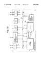
- FIG. 4which is a detailed circuit diagram of the control circuit 47 of FIG. 3, only a section for generating the control signal WE1 is illustrated; the other sections for generating the control signals WE2, ER1 and ER2 are similar to this section. That is, the control circuit 47 includes a timing generating circuit 471 for receiving the write enable signal WE1 to generate a start pulse ST in synchronization with a clock signal CK.
- a counter 472is initiated by receiving the start pulse ST to count the clock signal CK.
- a comparator 474compares the content of the counter 472 with a preset value in a register 473. As a result, when the content of the counter 472 coincides with the preset value of the register 473, the comparator 474 generates a stop pulse SP.
- a pulse generating circuit 475responds to the start pulse ST and the stop pulse SP. That is, the control signal WE1 rises in response to the start pulse ST and falls in response to the stop pulse SP.
- the preset value of the register 473is a definite value depending on the frequency of the clock signal CK. For example, the preset value corresponds to about 50 ⁇ s for the control signals WE1 and WE2, and corresponds to about 2 s for the control signals ER1 and ER2.
- the test of the writing operation, the writing verification operation, the flash erasing operation and the erasing verification operation of the flash EEPROM 4 under the CPU 7may be possible by operation of the ROM 6. In this case, however, since the ROM 6 includes a redundant program, it is impossible to effectively carry out such a test.
- the ROM 5is active only for an on-board writing operation mode; in other words, the ROM 6 is inactive for the other operation modes. Therefore, when the ROM 6 is incorporated into one chip of the microcomputer, the chip area thereof is increased, thus reducing the manufacturing yield.
- serial communication interface 2is fixed to one of the types of communication systems, an upper system is limited. If the microcomputer is forced to respond to all types of communication systems, a plurality of such types of serial communication interfaces have to be introduced into the chip of the microcomputer, thus making the control complex. Also, this increases the chip area, which reduces the manufacturing yield.
- control programsince the control program is temporarily stored in the RAM 5 or a buffer 7a of the CPU 7, the time of a writing operation of the control program is long.
- the time period of a writing operation and the time period of a flash erasing operationare determined by the preset value of the register 472 and the like. In this case, however, when the frequency of the clock signal CK is changed by the upper system or the type of the serial communication interface 2, the time period of a writing operation and the time period of a flash erasing operation are also changed.
- FIG. 5which illustrates a first embodiment of the microcomputer according to the present invention
- a switching circuit 8is interposed between the input/output port 1b and the internal buses and between the ROM 6 and the internal buses.
- the ROM 6has the same address space as an external circuit connected to the input/output port 1b.
- the switching circuit 8is controlled by the mode control circuit 3. That is, in an emulation test mode, the switching circuit 8 is operated so that the ROM 6 is deactivated and the input/output port 1b is activated.
- the operations of the microcomputer of FIG. 5are the same as those of the microcomputer of FIG. 1 except for an emulation test operation.
- the emulation Lest modeis illustrated in FIG. 6 where the deactivated blocks are removed from FIG. 5. That is, in advance of the emulation test operation, an emulation memory 21 is connected to the input/output port 1b, and an emulation test data source 22 is connected to the serial communication interface 2.
- the mode control unit 3recognizes an emulation test mode by the data signal at the data bus DB supplied from the input/output port 1a (not shown in FIG. 6, but shown in FIG. 5) or the like. As a result, the mode control unit 3 connects the serial communication interface 2, the flash EEPROM 4, the RAM 5 and the CPU 7 to the address bus AB, the data bus DB and the control bus.
- the mode control unit 3operates the switching circuit 8 so that the ROM 6 is deactivated and the input/output port 1b, i.e., the emulation memory 21 is activated. Therefore, the emulation memory 21 can be accessed by the same addresses for the ROM 6.
- the CPU 7reads an emulation test data via the serial communication interface 2 from the emulation test data source 22 in accordance with the emulation program stored in the emulation memory 21, and temporarily stores the emulation test data into the RAM 5. Then, the emulation test data is written into the flash EEPROM 4 at a predetermined timing. Note that the emulation test data program can be temporarily stored in the buffer of the CPU 7 instead of the RAM 5.
- a writing verification operationis carried out by the CPU 7 in accordance with the emulation program stored in the emulation memory 21.
- a determination of whether or not an on-board writing operation is normally carried outcan be done.
- the emulation program stored in the emulation memory 21 and the emulation memory 21 and the emulation test data stored in the emulation test data source 22are corrected, thus carrying out an on-board writing operation again.
- a writing program, a writing verification program, a flash erasing program and an erasing verification programare stored in the emulation memory 21. Therefore, the CPU 7 performs a writing operation, a writing verification operation, a flash earsing operation and an erasing verification operation upon the flash EEPROM 4 in accordance with the emulation program stored in the emulation memory 21.
- the write enable signal, the erase signal and the other timing signals from the CPU 7 to the flash EEPROM 4can be effectively tested.
- FIG. 7which illustrates a second embodiment of the microcomputer according to the present invention
- a writing program area 5ais provided in the RAM 5, and intead of this, the ROM 6 of FIG. 1 is removed. That is, at an initial state such as a power on state, the writing program area 5a is initialized to store a writing program in the writing program area 5a of the RAM 5.
- the RAM 5is formed by a static random access memory (SRAM) having flip-flop type cells, and the states of the flip-flop type cells of the writing program area 5a are fixed in advance. That is, since each cell is formed by two resistances and two cross-coupled driving transistors, if one of the resistances is made larger than the other, the state of this cell is fixed.
- SRAMstatic random access memory
- the CPU 7reads a control program via the serial communication interface 2 from the control program source 11 in accordance with the writing program stored in the writing program area 5a of the RAM 5, and temprorarily stores the control program into the RAM 5. Then, the control program is written into the flash EEPROM 4 at a predetermined timing. Note that the control program can be temporarily stored in the buffer 7a of the CPU 7 instead of the RAM 5.
- FIG. 9which illustrates a third embodiment of the microcomputer according to the present invention
- the serial communication interface 2 of FIG. 1is modified into a serial communication interface 2'.
- the serial communication interface 2'includes three types of interfaces, i.e., a synchronous three-wire communication interface 201, an asynchronous two-wire communication interface 202, and a synchronous IIC bus communication interface 203. Also, one of the interfaces 201, 202 and 203 is selected by a selector 204 which is controlled by a register 205. The content of the register 205 is set at a predetermined timing using the flash EEPROM 4 or the RAM 5 which is also set by a power on routine or the like.
- the register 205can be set directly by supplying voltages to terminals of the register 205.
- one of the interfaces 201, 202 and 203can be selected in accordance with the upper system, thus matching with the upper system.
- a data reception time detector 9is connected to the internal buses AB and DB, and the data reception time detector 9 is also connected to the CPU 7. That is, in an on-board writing operation mode, the data reception time detector 9 detects an interval time T between one piece of the control program and another piece of the control program, and transmits the interval time T to the CPU 7.
- the CPU 7reads a control program via the serial communication interface 2 from the control program source 11 (see FIG. 2B) in accordance with the writing program stored in the ROM 6. In this case, at each timing of reading one piece of the control program, the CPU 7 determines whether or not the interval time T is smaller than a definite time T0. As a result, if T ⁇ T0, which means that the data read speed is large, the CPU 7 temporarily stores the piece of the control program into the RAM 5. Then, the control program is written into the flash EEPROM 4 at a predetermined Liming. Note that the control program can be temporarily stored in the buffer 7a (see FIG. 2B) of the CPU 7 instead of the RAM 5. Contrary to this, if T ⁇ T0, which means that the data read speed is small, the CPU 7 directly writes the piece of the control program into the flash EEPROM 4. Thus, the operation speed of the on-board writing operation can be increased.
- FIG. 11Awhich illustrates a fifth embodiment of the microcomputer according to the present invention
- the content of the register 473 of FIG. 4can be changed, while the content of the register 473 in the prior art is fixed. That is, the content of the register 473 can be changed in accordance with the frequency of the clock signal CK.
- FIG. 11Bwhich is a modification of the control circuit 47 of FIG. 11A, a frequency-to-voltage conversion circuit 476 is connected to the register 473.
- the frequency-to-voltage conversion circuit 476generates a digital signal whose value is proportional to the frequency of the clock signal CK. Therefore, in the control circuit 47 of FIG. 11B, the content of the register 473 can be automatically set.
- the value of the frequency to voltage conversion circuit 476may be larger than the maximum value of the register 473. This is compensated for by circuits as illustrated in FIGS. 11C and 11D.
- a counter 477receives the output of the comparator 474 to count the clock signal CK. Then, when the content of the counter 477 reaches a predetermined value, the counter 477 generates a delayed stop pulse.
- the determination circuit 478determines whether or not the value of the frequency-to-voltage conversion circuit 476 is larger than a predetermined value corresponding to the maximum value of the register 473.
- the delay stop signal of the counter 477is transmitted via the gate circuits 480 and 481 selected by the determination circuit 478 to the pulse generating circuit 475.
- the maximum valueis set in the register 473.
- the output signal of the comparator 474is transmitted via the gate circuits 479 and 481 selected by the determination circuit 478 as the stop pulse to the pulse generating circuit 475.
- a determination 482which is the same as the determination circuit 478 of FIG. 11C, and a pulse eliminating circuit 483 are added to the elements of FIG. 11B.
- the pulse eliminating circuit 483eliminates a part of pulses of the clock signal CK.
- the pulse eliminating circuit 483is activated by the determination circuit 482, thus substantially delaying the generation of the stop pulse SP. In this case, the maximum value is also set in the register 473. Otherwise, the pulse eliminating circuit 483 is deactivated by the determination circuit 482, so that all pulses of the clock signal CK pass though the pulse eliminating circuit 483 and reach the counter 472.
- the write enable signal, the erase signal and the other timing signals from the CPU to the flash EEPROMare tested, it is possible to guarantee the operation of the flash EEPROM by the CPU.
- the function of the ROMis incorporated into the RAM, the chip area of the microcomputer is decreased, thus increasing the manufacturing yield.
- serial communication interfaceresponds to a plurality of types of serial communication interfaces, matching with any possible upper systems can be obtained.
- the operation speed of an on-board writing operation modeis adjusted in accordance with the read speed of a program from the serial communication interface, the operation speed of the on-board writing operation mode can be improved.
- the time period of a writing operation and the time period of a flash erasing operationcan be almost definite.
Landscapes
- Engineering & Computer Science (AREA)
- Theoretical Computer Science (AREA)
- General Engineering & Computer Science (AREA)
- Physics & Mathematics (AREA)
- General Physics & Mathematics (AREA)
- Quality & Reliability (AREA)
- Computer Hardware Design (AREA)
- Microcomputers (AREA)
- Read Only Memory (AREA)
- Techniques For Improving Reliability Of Storages (AREA)
- Test And Diagnosis Of Digital Computers (AREA)
- For Increasing The Reliability Of Semiconductor Memories (AREA)
Abstract
Description
Claims (26)
Applications Claiming Priority (2)
| Application Number | Priority Date | Filing Date | Title |
|---|---|---|---|
| JP7-293127 | 1995-11-10 | ||
| JP29312795AJP3693721B2 (en) | 1995-11-10 | 1995-11-10 | Microcomputer with built-in flash memory and test method thereof |
Publications (1)
| Publication Number | Publication Date |
|---|---|
| US5872994Atrue US5872994A (en) | 1999-02-16 |
Family
ID=17790775
Family Applications (1)
| Application Number | Title | Priority Date | Filing Date |
|---|---|---|---|
| US08/745,828Expired - LifetimeUS5872994A (en) | 1995-11-10 | 1996-11-12 | Flash memory incorporating microcomputer having on-board writing function |
Country Status (5)
| Country | Link |
|---|---|
| US (1) | US5872994A (en) |
| EP (1) | EP0775956B1 (en) |
| JP (1) | JP3693721B2 (en) |
| KR (1) | KR100217215B1 (en) |
| DE (1) | DE69621403T2 (en) |
Cited By (143)
| Publication number | Priority date | Publication date | Assignee | Title |
|---|---|---|---|---|
| US6286101B1 (en)* | 1997-09-05 | 2001-09-04 | Mitsubishi Denki Kabushiki Kaisha | Central processing unit and microcomputer system having an internal operation unit for cryptographic |
| US20020082824A1 (en)* | 2000-12-27 | 2002-06-27 | Gilbert Neiger | Virtual translation lookaside buffer |
| US6480928B2 (en)* | 2000-03-16 | 2002-11-12 | Honda Giken Kogyo Kabushiki Kaisha | Memory rewriting system for vehicle controller |
| US6480432B1 (en)* | 1998-12-25 | 2002-11-12 | Fujitsu Limited | Flash memory device having mask ROM cells for self-test |
| US6532019B1 (en) | 1998-06-17 | 2003-03-11 | Advanced Micro Devices, Inc. | Input/output integrated circuit hub incorporating a RAMDAC |
| US20030107922A1 (en)* | 2001-12-06 | 2003-06-12 | Tung-Cheng Kuo | Method for fabricating embedded flash ROM structure having code cells and data cells and operations for the same |
| KR100388219B1 (en)* | 2000-08-29 | 2003-06-19 | 주식회사 하이닉스반도체 | Flash memory embeded one-chip micro controller unit |
| US20030115453A1 (en)* | 2001-12-17 | 2003-06-19 | Grawrock David W. | Connecting a virtual token to a physical token |
| US20030120856A1 (en)* | 2000-12-27 | 2003-06-26 | Gilbert Neiger | Method for resolving address space conflicts between a virtual machine monitor and a guest operating system |
| US20030126454A1 (en)* | 2001-12-28 | 2003-07-03 | Glew Andrew F. | Authenticated code method and apparatus |
| US20030135687A1 (en)* | 2002-01-15 | 2003-07-17 | Owens Brian Keith | Memory module, printer assembly, and method for storing printer code |
| US6614684B1 (en)* | 1999-02-01 | 2003-09-02 | Hitachi, Ltd. | Semiconductor integrated circuit and nonvolatile memory element |
| US20030191943A1 (en)* | 2002-04-05 | 2003-10-09 | Poisner David I. | Methods and arrangements to register code |
| US6633963B1 (en) | 2000-03-31 | 2003-10-14 | Intel Corporation | Controlling access to multiple memory zones in an isolated execution environment |
| US20030196088A1 (en)* | 2002-04-15 | 2003-10-16 | Poisner David I. | Method and apparatus for communicating securely with a token |
| US20030196083A1 (en)* | 2002-04-15 | 2003-10-16 | Grawrock David W. | Validation of inclusion of a platform within a data center |
| US20030233550A1 (en)* | 2002-06-18 | 2003-12-18 | Brickell Ernie F. | Method of confirming a secure key exchange |
| US20040003273A1 (en)* | 2002-06-26 | 2004-01-01 | Grawrock David W. | Sleep protection |
| KR20040002143A (en)* | 2002-06-29 | 2004-01-07 | 주식회사 하이닉스반도체 | Flash memory controller |
| US6678825B1 (en) | 2000-03-31 | 2004-01-13 | Intel Corporation | Controlling access to multiple isolated memories in an isolated execution environment |
| US20040039491A1 (en)* | 2000-09-20 | 2004-02-26 | Martin Hurich | Control device for controlling/regulating the operational sequences in a motor vehicle, and a method of starting such a control device |
| US20040073846A1 (en)* | 2002-01-31 | 2004-04-15 | Yoshiaki Nakanishi | Memory device, terminal apparatus, and data repair system |
| US20040078590A1 (en)* | 2000-03-31 | 2004-04-22 | Ellison Carl M. | Controlling access to multiple memory zones in an isolated execution environment |
| US20040117593A1 (en)* | 2002-12-12 | 2004-06-17 | Richard Uhlig | Reclaiming existing fields in address translation data structures to extend control over memory acceses |
| US20040117318A1 (en)* | 2002-12-16 | 2004-06-17 | Grawrock David W. | Portable token controlling trusted environment launch |
| US20040117532A1 (en)* | 2002-12-11 | 2004-06-17 | Bennett Steven M. | Mechanism for controlling external interrupts in a virtual machine system |
| US6754815B1 (en) | 2000-03-31 | 2004-06-22 | Intel Corporation | Method and system for scrubbing an isolated area of memory after reset of a processor operating in isolated execution mode if a cleanup flag is set |
| US20040123288A1 (en)* | 2002-12-19 | 2004-06-24 | Intel Corporation | Methods and systems to manage machine state in virtual machine operations |
| US20040128465A1 (en)* | 2002-12-30 | 2004-07-01 | Lee Micheil J. | Configurable memory bus width |
| US20040128345A1 (en)* | 2002-12-27 | 2004-07-01 | Robinson Scott H. | Dynamic service registry |
| US6760441B1 (en) | 2000-03-31 | 2004-07-06 | Intel Corporation | Generating a key hieararchy for use in an isolated execution environment |
| US6769058B1 (en) | 2000-03-31 | 2004-07-27 | Intel Corporation | Resetting a processor in an isolated execution environment |
| US6795905B1 (en)* | 2000-03-31 | 2004-09-21 | Intel Corporation | Controlling accesses to isolated memory using a memory controller for isolated execution |
| US6820177B2 (en) | 2002-06-12 | 2004-11-16 | Intel Corporation | Protected configuration space in a protected environment |
| US20040268347A1 (en)* | 2003-06-26 | 2004-12-30 | Knauerhase Robert C. | Virtual machine management using processor state information |
| US6839774B1 (en) | 1999-10-21 | 2005-01-04 | Samsung Electronics Co., Ltd. | Single-chip data processing apparatus incorporating an electrically rewritable nonvolatile memory and method of operating the same |
| US20050044292A1 (en)* | 2003-08-19 | 2005-02-24 | Mckeen Francis X. | Method and apparatus to retain system control when a buffer overflow attack occurs |
| US20050055481A1 (en)* | 2003-09-10 | 2005-03-10 | Super Talent Flash, Inc | Flash drive/reader with serial-port controller and flash-memory controller mastering a second ram-buffer bus parallel to a cpu bus |
| US20050060703A1 (en)* | 2003-09-15 | 2005-03-17 | Bennett Steven M. | Vectoring an interrupt or exception upon resuming operation of a virtual machine |
| US20050080970A1 (en)* | 2003-09-30 | 2005-04-14 | Stalinselvaraj Jeyasingh | Chipset support for managing hardware interrupts in a virtual machine system |
| US20050080934A1 (en)* | 2003-09-30 | 2005-04-14 | Cota-Robles Erik C. | Invalidating translation lookaside buffer entries in a virtual machine (VM) system |
| US20050084098A1 (en)* | 2003-09-18 | 2005-04-21 | Brickell Ernie F. | Method of obscuring cryptographic computations |
| US20050086508A1 (en)* | 2003-09-19 | 2005-04-21 | Moran Douglas R. | Prioritized address decoder |
| US20050108534A1 (en)* | 2003-11-19 | 2005-05-19 | Bajikar Sundeep M. | Providing services to an open platform implementing subscriber identity module (SIM) capabilities |
| US20050108532A1 (en)* | 2003-11-17 | 2005-05-19 | Bajikar Sundeep M. | Method and system to provide a trusted channel within a computer system for a SIM device |
| US20050108171A1 (en)* | 2003-11-19 | 2005-05-19 | Bajikar Sundeep M. | Method and apparatus for implementing subscriber identity module (SIM) capabilities in an open platform |
| US6904400B1 (en)* | 1998-09-30 | 2005-06-07 | Stmicroelectronics S.R.L. | Flash EEPROM memory emulator of non-flash EEPROM device and corresponding method |
| US20050137898A1 (en)* | 2003-12-22 | 2005-06-23 | Wood Matthew D. | Replacing blinded authentication authority |
| US20050152539A1 (en)* | 2004-01-12 | 2005-07-14 | Brickell Ernie F. | Method of protecting cryptographic operations from side channel attacks |
| US20050182940A1 (en)* | 2002-03-29 | 2005-08-18 | Sutton James A.Ii | System and method for execution of a secured environment initialization instruction |
| US20050188198A1 (en)* | 2000-03-31 | 2005-08-25 | Ellison Carl M. | Managing a secure platform using a hierarchical executive architecture in isolated execution mode |
| US20050216920A1 (en)* | 2004-03-24 | 2005-09-29 | Vijay Tewari | Use of a virtual machine to emulate a hardware device |
| US20050240700A1 (en)* | 2004-03-31 | 2005-10-27 | Bennett Steven M | Method and apparatus for facilitating recognition of an open event window during operation of guest software in a virtual machine environment |
| US20050240819A1 (en)* | 2004-03-30 | 2005-10-27 | Bennett Steven M | Providing support for single stepping a virtual machine in a virtual machine environment |
| US20050283660A1 (en)* | 2000-09-28 | 2005-12-22 | Mckeen Francis X | Mechanism to handle events in a machine with isolated execution |
| US20050288056A1 (en)* | 2004-06-29 | 2005-12-29 | Bajikar Sundeep M | System including a wireless wide area network (WWAN) module with an external identity module reader and approach for certifying the WWAN module |
| US20060005084A1 (en)* | 2004-06-30 | 2006-01-05 | Gilbert Neiger | Support for nested faults in a virtual machine environment |
| US6990579B1 (en) | 2000-03-31 | 2006-01-24 | Intel Corporation | Platform and method for remote attestation of a platform |
| US6996710B1 (en) | 2000-03-31 | 2006-02-07 | Intel Corporation | Platform and method for issuing and certifying a hardware-protected attestation key |
| US6996748B2 (en) | 2002-06-29 | 2006-02-07 | Intel Corporation | Handling faults associated with operation of guest software in the virtual-machine architecture |
| US7013481B1 (en) | 2000-03-31 | 2006-03-14 | Intel Corporation | Attestation key memory device and bus |
| US7013484B1 (en) | 2000-03-31 | 2006-03-14 | Intel Corporation | Managing a secure environment using a chipset in isolated execution mode |
| US7024555B2 (en) | 2001-11-01 | 2006-04-04 | Intel Corporation | Apparatus and method for unilaterally loading a secure operating system within a multiprocessor environment |
| US20060075402A1 (en)* | 2004-09-30 | 2006-04-06 | Gilbert Neiger | Providing support for a timer associated with a virtual machine monitor |
| US7028149B2 (en) | 2002-03-29 | 2006-04-11 | Intel Corporation | System and method for resetting a platform configuration register |
| US20060080528A1 (en)* | 2000-06-28 | 2006-04-13 | Ellison Carl M | Platform and method for establishing provable identities while maintaining privacy |
| US20060083069A1 (en)* | 2004-09-30 | 2006-04-20 | Matrix Semiconductor, Inc. | System and method of controlling a three-dimensional memory |
| US20060117181A1 (en)* | 2004-11-30 | 2006-06-01 | Brickell Ernest F | Apparatus and method for establishing a secure session with a device without exposing privacy-sensitive information |
| US7073071B1 (en) | 2000-03-31 | 2006-07-04 | Intel Corporation | Platform and method for generating and utilizing a protected audit log |
| US7082615B1 (en) | 2000-03-31 | 2006-07-25 | Intel Corporation | Protecting software environment in isolated execution |
| US7089418B1 (en) | 2000-03-31 | 2006-08-08 | Intel Corporation | Managing accesses in a processor for isolated execution |
| US7096497B2 (en) | 2001-03-30 | 2006-08-22 | Intel Corporation | File checking using remote signing authority via a network |
| US7111176B1 (en) | 2000-03-31 | 2006-09-19 | Intel Corporation | Generating isolated bus cycles for isolated execution |
| US7117376B2 (en) | 2000-12-28 | 2006-10-03 | Intel Corporation | Platform and method of creating a secure boot that enforces proper user authentication and enforces hardware configurations |
| US7124327B2 (en) | 2002-06-29 | 2006-10-17 | Intel Corporation | Control over faults occurring during the operation of guest software in the virtual-machine architecture |
| US7127548B2 (en) | 2002-04-16 | 2006-10-24 | Intel Corporation | Control register access virtualization performance improvement in the virtual-machine architecture |
| US7139890B2 (en) | 2002-04-30 | 2006-11-21 | Intel Corporation | Methods and arrangements to interface memory |
| US7165181B2 (en) | 2002-11-27 | 2007-01-16 | Intel Corporation | System and method for establishing trust without revealing identity |
| US7191440B2 (en) | 2001-08-15 | 2007-03-13 | Intel Corporation | Tracking operating system process and thread execution and virtual machine execution in hardware or in a virtual machine monitor |
| US20070061524A1 (en)* | 2005-09-15 | 2007-03-15 | Microchip Technology Incorporated | Programming a digital processor with a single connection |
| US7194634B2 (en) | 2000-03-31 | 2007-03-20 | Intel Corporation | Attestation key memory device and bus |
| US20070076479A1 (en)* | 2005-09-30 | 2007-04-05 | Mosaid Technologies Incorporated | Multiple independent serial link memory |
| WO2007036050A1 (en)* | 2005-09-30 | 2007-04-05 | Mosaid Technologies Incorporated | Memory with output control |
| US20070076502A1 (en)* | 2005-09-30 | 2007-04-05 | Pyeon Hong B | Daisy chain cascading devices |
| US7215781B2 (en) | 2000-12-22 | 2007-05-08 | Intel Corporation | Creation and distribution of a secret value between two devices |
| US7225441B2 (en) | 2000-12-27 | 2007-05-29 | Intel Corporation | Mechanism for providing power management through virtualization |
| US7237051B2 (en) | 2003-09-30 | 2007-06-26 | Intel Corporation | Mechanism to control hardware interrupt acknowledgement in a virtual machine system |
| US20070165457A1 (en)* | 2005-09-30 | 2007-07-19 | Jin-Ki Kim | Nonvolatile memory system |
| US20070233903A1 (en)* | 2006-03-28 | 2007-10-04 | Hong Beom Pyeon | Daisy chain cascade configuration recognition technique |
| US20070233917A1 (en)* | 2006-03-28 | 2007-10-04 | Mosaid Technologies Incorporated | Apparatus and method for establishing device identifiers for serially interconnected devices |
| US20070233939A1 (en)* | 2006-03-31 | 2007-10-04 | Mosaid Technologies Incorporated | Flash memory system control scheme |
| US20070230253A1 (en)* | 2006-03-29 | 2007-10-04 | Jin-Ki Kim | Non-volatile semiconductor memory with page erase |
| US20070234071A1 (en)* | 2006-03-28 | 2007-10-04 | Mosaid Technologies Incorporated | Asynchronous ID generation |
| US7296267B2 (en) | 2002-07-12 | 2007-11-13 | Intel Corporation | System and method for binding virtual machines to hardware contexts |
| US7308576B2 (en) | 2001-12-31 | 2007-12-11 | Intel Corporation | Authenticated code module |
| US7318235B2 (en) | 2002-12-16 | 2008-01-08 | Intel Corporation | Attestation using both fixed token and portable token |
| US7318141B2 (en) | 2002-12-17 | 2008-01-08 | Intel Corporation | Methods and systems to control virtual machines |
| US20080052453A1 (en)* | 2000-02-21 | 2008-02-28 | Trek 2000 International Ltd. | Portable data storage device |
| US20080080492A1 (en)* | 2006-09-29 | 2008-04-03 | Mosaid Technologies Incorporated | Packet based ID generation for serially interconnected devices |
| US7356817B1 (en) | 2000-03-31 | 2008-04-08 | Intel Corporation | Real-time scheduling of virtual machines |
| US7366305B2 (en) | 2003-09-30 | 2008-04-29 | Intel Corporation | Platform and method for establishing trust without revealing identity |
| US20080123423A1 (en)* | 2006-11-27 | 2008-05-29 | Mosaid Technologies Incorporated | Non-volatile memory serial core architecture |
| US20080140948A1 (en)* | 2006-12-06 | 2008-06-12 | Mosaid Technologies Incorporated | Apparatus and method for producing device identifiers for serially interconnected devices of mixed type |
| US20080137467A1 (en)* | 2006-12-06 | 2008-06-12 | Mosaid Technologies Incorporated | Apparatus and method for capturing serial input data |
| US20080137461A1 (en)* | 2006-12-12 | 2008-06-12 | Hong Beom Pyeon | Memory system and method with serial and parallel modes |
| US7389427B1 (en) | 2000-09-28 | 2008-06-17 | Intel Corporation | Mechanism to secure computer output from software attack using isolated execution |
| US20080155219A1 (en)* | 2006-12-20 | 2008-06-26 | Mosaid Technologies Incorporated | Id generation apparatus and method for serially interconnected devices |
| US20080155179A1 (en)* | 2006-12-06 | 2008-06-26 | Mosaid Technologies Incorporated | Apparatus and method for producing ids for interconnected devices of mixed type |
| US7395405B2 (en) | 2005-01-28 | 2008-07-01 | Intel Corporation | Method and apparatus for supporting address translation in a virtual machine environment |
| US20080181214A1 (en)* | 2006-12-06 | 2008-07-31 | Mosaid Technologies Incorporated | Apparatus and method for producing device identifiers for serially interconnected devices of mixed type |
| US20080195613A1 (en)* | 2007-02-13 | 2008-08-14 | Mosaid Technologies Incorporated | Apparatus and method for identifying device types of series-connected devices of mixed type |
| US20080198682A1 (en)* | 2007-02-16 | 2008-08-21 | Mosaid Technologies Incorporated | Semiconductor device and method for selection and de-selection of memory devices interconnected in series |
| US20080205187A1 (en)* | 2007-02-22 | 2008-08-28 | Mosaid Technologies Incorporated | Data flow control in multiple independent port |
| US20080209110A1 (en)* | 2007-02-22 | 2008-08-28 | Mosaid Technologies Incorporated | Apparatus and method of page program operation for memory devices with mirror back-up of data |
| US20080209108A1 (en)* | 2007-02-22 | 2008-08-28 | Hong Beom Pyeon | System and method of page buffer operation for memory devices |
| US7424709B2 (en) | 2003-09-15 | 2008-09-09 | Intel Corporation | Use of multiple virtual machine monitors to handle privileged events |
| US20080250191A1 (en)* | 2007-04-04 | 2008-10-09 | Atmel Corporation | Flexible, low cost apparatus and method to introduce and check algorithm modifications in a non-volatile memory |
| US7480806B2 (en) | 2002-02-22 | 2009-01-20 | Intel Corporation | Multi-token seal and unseal |
| US7490070B2 (en) | 2004-06-10 | 2009-02-10 | Intel Corporation | Apparatus and method for proving the denial of a direct proof signature |
| US20090138768A1 (en)* | 2007-11-23 | 2009-05-28 | Mosaid Technologies Incorporated | Data channel test apparatus and method thereof |
| US20090154284A1 (en)* | 2007-12-12 | 2009-06-18 | Hakjune Oh | Semiconductor memory device suitable for interconnection in a ring topology |
| US20090161451A1 (en)* | 2007-12-20 | 2009-06-25 | Mosaid Technologies Incorporated | Dual function compatible non-volatile memory device |
| US20090175081A1 (en)* | 2008-01-07 | 2009-07-09 | Mosaid Technologies Incorporated | Nand flash memory having multiple cell substrates |
| US20090290436A1 (en)* | 2005-09-28 | 2009-11-26 | Hwang Hur | Test circuit for multi-port memory device |
| US20090300273A1 (en)* | 2008-06-02 | 2009-12-03 | Ming-Dar Chen | Flash memory apparatus with automatic interface mode switching |
| US7631196B2 (en) | 2002-02-25 | 2009-12-08 | Intel Corporation | Method and apparatus for loading a trustable operating system |
| US7747833B2 (en) | 2005-09-30 | 2010-06-29 | Mosaid Technologies Incorporated | Independent link and bank selection |
| CN101055768B (en)* | 2006-04-13 | 2010-08-04 | 海力士半导体有限公司 | Semiconductor memory device |
| US20100202224A1 (en)* | 2007-07-18 | 2010-08-12 | Hakjune Oh | Memory with data control |
| US7802085B2 (en) | 2004-02-18 | 2010-09-21 | Intel Corporation | Apparatus and method for distributing private keys to an entity with minimal secret, unique information |
| US7809957B2 (en) | 2005-09-29 | 2010-10-05 | Intel Corporation | Trusted platform module for generating sealed data |
| US7818808B1 (en) | 2000-12-27 | 2010-10-19 | Intel Corporation | Processor mode for limiting the operation of guest software running on a virtual machine supported by a virtual machine monitor |
| US7853727B2 (en) | 2006-12-06 | 2010-12-14 | Mosaid Technologies Incorporated | Apparatus and method for producing identifiers regardless of mixed device type in a serial interconnection |
| US7900017B2 (en) | 2002-12-27 | 2011-03-01 | Intel Corporation | Mechanism for remapping post virtual machine memory pages |
| US20110131383A1 (en)* | 2006-08-22 | 2011-06-02 | Mosaid Technologies Incorporated | Modular command structure for memory and memory system |
| US8014530B2 (en) | 2006-03-22 | 2011-09-06 | Intel Corporation | Method and apparatus for authenticated, recoverable key distribution with no database secrets |
| US8146078B2 (en) | 2004-10-29 | 2012-03-27 | Intel Corporation | Timer offsetting mechanism in a virtual machine environment |
| US8156343B2 (en) | 2003-11-26 | 2012-04-10 | Intel Corporation | Accessing private data about the state of a data processing machine from storage that is publicly accessible |
| US8533777B2 (en) | 2004-12-29 | 2013-09-10 | Intel Corporation | Mechanism to determine trust of out-of-band management agents |
| US8825967B2 (en) | 2011-12-08 | 2014-09-02 | Conversant Intellectual Property Management Inc. | Independent write and read control in serially-connected devices |
| CN103050150B (en)* | 2012-12-31 | 2015-11-18 | 中国电子科技集团公司第十五研究所 | Flash interface circuit |
| CN115480959A (en)* | 2021-05-31 | 2022-12-16 | 西安紫光国芯半导体有限公司 | Storage test method, storage chip and related equipment based on serial interface |
| US11948629B2 (en) | 2005-09-30 | 2024-04-02 | Mosaid Technologies Incorporated | Non-volatile memory device with concurrent bank operations |
Families Citing this family (4)
| Publication number | Priority date | Publication date | Assignee | Title |
|---|---|---|---|---|
| DE19740525C1 (en)* | 1997-09-15 | 1999-02-04 | Siemens Ag | Method of data storage and recovery in control system, esp. in motor vehicle, such as taxi |
| JP2000112918A (en) | 1998-10-09 | 2000-04-21 | Nec Corp | Micro computer incoroprating flash eeprom |
| US6148354A (en) | 1999-04-05 | 2000-11-14 | M-Systems Flash Disk Pioneers Ltd. | Architecture for a universal serial bus-based PC flash disk |
| JP5855616B2 (en)* | 2013-09-12 | 2016-02-09 | 大日本印刷株式会社 | Circuit board inspection method, circuit board inspection device |
Citations (5)
| Publication number | Priority date | Publication date | Assignee | Title |
|---|---|---|---|---|
| US4809167A (en)* | 1985-07-03 | 1989-02-28 | Metalink Corporation | Circuitry for emulating single chip microcomputer without access to internal buses |
| EP0402682A2 (en)* | 1989-06-15 | 1990-12-19 | Societe Des Produits Nestle S.A. | Method and apparatus for cooking, pasteurizing and chilling meat |
| JPH05266219A (en)* | 1992-03-17 | 1993-10-15 | Hitachi Ltd | Microcomputer |
| US5459850A (en)* | 1993-02-19 | 1995-10-17 | Conner Peripherals, Inc. | Flash solid state drive that emulates a disk drive and stores variable length and fixed lenth data blocks |
| US5535328A (en)* | 1989-04-13 | 1996-07-09 | Sandisk Corporation | Non-volatile memory system card with flash erasable sectors of EEprom cells including a mechanism for substituting defective cells |
Family Cites Families (1)
| Publication number | Priority date | Publication date | Assignee | Title |
|---|---|---|---|---|
| US5210854A (en)* | 1989-06-14 | 1993-05-11 | Digital Equipment Corporation | System for updating program stored in eeprom by storing new version into new location and updating second transfer vector to contain starting address of new version |
- 1995
- 1995-11-10JPJP29312795Apatent/JP3693721B2/ennot_activeExpired - Fee Related
- 1996
- 1996-11-08DEDE69621403Tpatent/DE69621403T2/ennot_activeExpired - Fee Related
- 1996-11-08EPEP96117979Apatent/EP0775956B1/ennot_activeExpired - Lifetime
- 1996-11-11KRKR1019960054761Apatent/KR100217215B1/ennot_activeExpired - Fee Related
- 1996-11-12USUS08/745,828patent/US5872994A/ennot_activeExpired - Lifetime
Patent Citations (5)
| Publication number | Priority date | Publication date | Assignee | Title |
|---|---|---|---|---|
| US4809167A (en)* | 1985-07-03 | 1989-02-28 | Metalink Corporation | Circuitry for emulating single chip microcomputer without access to internal buses |
| US5535328A (en)* | 1989-04-13 | 1996-07-09 | Sandisk Corporation | Non-volatile memory system card with flash erasable sectors of EEprom cells including a mechanism for substituting defective cells |
| EP0402682A2 (en)* | 1989-06-15 | 1990-12-19 | Societe Des Produits Nestle S.A. | Method and apparatus for cooking, pasteurizing and chilling meat |
| JPH05266219A (en)* | 1992-03-17 | 1993-10-15 | Hitachi Ltd | Microcomputer |
| US5459850A (en)* | 1993-02-19 | 1995-10-17 | Conner Peripherals, Inc. | Flash solid state drive that emulates a disk drive and stores variable length and fixed lenth data blocks |
Cited By (325)
| Publication number | Priority date | Publication date | Assignee | Title |
|---|---|---|---|---|
| US6286101B1 (en)* | 1997-09-05 | 2001-09-04 | Mitsubishi Denki Kabushiki Kaisha | Central processing unit and microcomputer system having an internal operation unit for cryptographic |
| US6532019B1 (en) | 1998-06-17 | 2003-03-11 | Advanced Micro Devices, Inc. | Input/output integrated circuit hub incorporating a RAMDAC |
| US6904400B1 (en)* | 1998-09-30 | 2005-06-07 | Stmicroelectronics S.R.L. | Flash EEPROM memory emulator of non-flash EEPROM device and corresponding method |
| US6480432B1 (en)* | 1998-12-25 | 2002-11-12 | Fujitsu Limited | Flash memory device having mask ROM cells for self-test |
| US20080037323A1 (en)* | 1999-02-01 | 2008-02-14 | Shoji Shukuri | Semiconductor integrated circuit and nonvolatile memory element |
| US20040190339A1 (en)* | 1999-02-01 | 2004-09-30 | Shoji Shukuri | Semiconductor integrated circuit and nonvolatile memory element |
| US20050232008A1 (en)* | 1999-02-01 | 2005-10-20 | Shoji Shukuri | Semiconductor integrated circuit and nonvolatile memory element |
| US6906954B2 (en) | 1999-02-01 | 2005-06-14 | Renesas Technology Corp. | Semiconductor integrated circuit and nonvolatile memory element |
| US6771538B2 (en) | 1999-02-01 | 2004-08-03 | Renesas Technology Corp. | Semiconductor integrated circuit and nonvolatile memory element |
| US20040004894A1 (en)* | 1999-02-01 | 2004-01-08 | Shoji Shukuri | Semiconductor integrated circuit and nonvolatile memory element |
| US7042764B2 (en) | 1999-02-01 | 2006-05-09 | Renesas Technology Corp. | Semiconductor integrated circuit and nonvolatile memory element |
| US6614684B1 (en)* | 1999-02-01 | 2003-09-02 | Hitachi, Ltd. | Semiconductor integrated circuit and nonvolatile memory element |
| US7289361B2 (en) | 1999-02-01 | 2007-10-30 | Renesas Technology Corp. | Semiconductor integrated circuit and nonvolatile memory element |
| US20060221688A1 (en)* | 1999-02-01 | 2006-10-05 | Shoji Shukuri | Semiconductor integrated circuit and nonvolatile memory element |
| US20060202274A1 (en)* | 1999-02-01 | 2006-09-14 | Shoji Shukuri | Semiconductor integrated circuit and nonvolatile memory element |
| US7463517B2 (en) | 1999-02-01 | 2008-12-09 | Renesas Technology Corp. | Semiconductor integrated circuit and nonvolatile memory element |
| US7428167B2 (en) | 1999-02-01 | 2008-09-23 | Renesas Technology Corp. | Semiconductor integrated circuit and nonvolatile memory element |
| US6839774B1 (en) | 1999-10-21 | 2005-01-04 | Samsung Electronics Co., Ltd. | Single-chip data processing apparatus incorporating an electrically rewritable nonvolatile memory and method of operating the same |
| US8209462B2 (en)* | 2000-02-21 | 2012-06-26 | Trek 2000 International Ltd. | Portable data storage device |
| US20080059660A1 (en)* | 2000-02-21 | 2008-03-06 | Trek 2000 International Ltd. | Portable data storage device |
| US20080052453A1 (en)* | 2000-02-21 | 2008-02-28 | Trek 2000 International Ltd. | Portable data storage device |
| US6480928B2 (en)* | 2000-03-16 | 2002-11-12 | Honda Giken Kogyo Kabushiki Kaisha | Memory rewriting system for vehicle controller |
| US6769058B1 (en) | 2000-03-31 | 2004-07-27 | Intel Corporation | Resetting a processor in an isolated execution environment |
| US7356817B1 (en) | 2000-03-31 | 2008-04-08 | Intel Corporation | Real-time scheduling of virtual machines |
| US20040078590A1 (en)* | 2000-03-31 | 2004-04-22 | Ellison Carl M. | Controlling access to multiple memory zones in an isolated execution environment |
| US6990579B1 (en) | 2000-03-31 | 2006-01-24 | Intel Corporation | Platform and method for remote attestation of a platform |
| US7194634B2 (en) | 2000-03-31 | 2007-03-20 | Intel Corporation | Attestation key memory device and bus |
| US6957332B1 (en) | 2000-03-31 | 2005-10-18 | Intel Corporation | Managing a secure platform using a hierarchical executive architecture in isolated execution mode |
| US6754815B1 (en) | 2000-03-31 | 2004-06-22 | Intel Corporation | Method and system for scrubbing an isolated area of memory after reset of a processor operating in isolated execution mode if a cleanup flag is set |
| US6996710B1 (en) | 2000-03-31 | 2006-02-07 | Intel Corporation | Platform and method for issuing and certifying a hardware-protected attestation key |
| US6941458B1 (en)* | 2000-03-31 | 2005-09-06 | Intel Corporation | Managing a secure platform using a hierarchical executive architecture in isolated execution mode |
| US7111176B1 (en) | 2000-03-31 | 2006-09-19 | Intel Corporation | Generating isolated bus cycles for isolated execution |
| US6760441B1 (en) | 2000-03-31 | 2004-07-06 | Intel Corporation | Generating a key hieararchy for use in an isolated execution environment |
| US20050188198A1 (en)* | 2000-03-31 | 2005-08-25 | Ellison Carl M. | Managing a secure platform using a hierarchical executive architecture in isolated execution mode |
| US6678825B1 (en) | 2000-03-31 | 2004-01-13 | Intel Corporation | Controlling access to multiple isolated memories in an isolated execution environment |
| US6795905B1 (en)* | 2000-03-31 | 2004-09-21 | Intel Corporation | Controlling accesses to isolated memory using a memory controller for isolated execution |
| US6934817B2 (en) | 2000-03-31 | 2005-08-23 | Intel Corporation | Controlling access to multiple memory zones in an isolated execution environment |
| US7013481B1 (en) | 2000-03-31 | 2006-03-14 | Intel Corporation | Attestation key memory device and bus |
| US7013484B1 (en) | 2000-03-31 | 2006-03-14 | Intel Corporation | Managing a secure environment using a chipset in isolated execution mode |
| US6633963B1 (en) | 2000-03-31 | 2003-10-14 | Intel Corporation | Controlling access to multiple memory zones in an isolated execution environment |
| US7089418B1 (en) | 2000-03-31 | 2006-08-08 | Intel Corporation | Managing accesses in a processor for isolated execution |
| US7085935B1 (en) | 2000-03-31 | 2006-08-01 | Intel Corporation | Managing a secure environment using a chipset in isolated execution mode |
| US7082615B1 (en) | 2000-03-31 | 2006-07-25 | Intel Corporation | Protecting software environment in isolated execution |
| US7073071B1 (en) | 2000-03-31 | 2006-07-04 | Intel Corporation | Platform and method for generating and utilizing a protected audit log |
| US7516330B2 (en) | 2000-06-28 | 2009-04-07 | Intel Corporation | Platform and method for establishing provable identities while maintaining privacy |
| US20060080528A1 (en)* | 2000-06-28 | 2006-04-13 | Ellison Carl M | Platform and method for establishing provable identities while maintaining privacy |
| KR100388219B1 (en)* | 2000-08-29 | 2003-06-19 | 주식회사 하이닉스반도체 | Flash memory embeded one-chip micro controller unit |
| US7016769B2 (en)* | 2000-09-20 | 2006-03-21 | Robert Bosch Gmbh | Control device for controlling/regulating the operational sequences in a motor vehicle, and a method of starting such a control device |
| US20040039491A1 (en)* | 2000-09-20 | 2004-02-26 | Martin Hurich | Control device for controlling/regulating the operational sequences in a motor vehicle, and a method of starting such a control device |
| US20100325445A1 (en)* | 2000-09-28 | 2010-12-23 | Mckeen Francis X | Mechanism to handle events in a machine with isolated execution |
| US8671275B2 (en) | 2000-09-28 | 2014-03-11 | Intel Corporation | Mechanism to handle events in a machine with isolated execution |
| US8522044B2 (en) | 2000-09-28 | 2013-08-27 | Intel Corporation | Mechanism to handle events in a machine with isolated execution |
| US20050283660A1 (en)* | 2000-09-28 | 2005-12-22 | Mckeen Francis X | Mechanism to handle events in a machine with isolated execution |
| US7793111B1 (en) | 2000-09-28 | 2010-09-07 | Intel Corporation | Mechanism to handle events in a machine with isolated execution |
| US7389427B1 (en) | 2000-09-28 | 2008-06-17 | Intel Corporation | Mechanism to secure computer output from software attack using isolated execution |
| US7215781B2 (en) | 2000-12-22 | 2007-05-08 | Intel Corporation | Creation and distribution of a secret value between two devices |
| US7313669B2 (en) | 2000-12-27 | 2007-12-25 | Intel Corporation | Virtual translation lookaside buffer |
| US6907600B2 (en) | 2000-12-27 | 2005-06-14 | Intel Corporation | Virtual translation lookaside buffer |
| US7225441B2 (en) | 2000-12-27 | 2007-05-29 | Intel Corporation | Mechanism for providing power management through virtualization |
| US7818808B1 (en) | 2000-12-27 | 2010-10-19 | Intel Corporation | Processor mode for limiting the operation of guest software running on a virtual machine supported by a virtual machine monitor |
| US20040064813A1 (en)* | 2000-12-27 | 2004-04-01 | Gilbert Neiger | Method for resolving address space conflicts between a virtual machine monitor and a guest operating system |
| US7035963B2 (en) | 2000-12-27 | 2006-04-25 | Intel Corporation | Method for resolving address space conflicts between a virtual machine monitor and a guest operating system |
| US20020082824A1 (en)* | 2000-12-27 | 2002-06-27 | Gilbert Neiger | Virtual translation lookaside buffer |
| US20030120856A1 (en)* | 2000-12-27 | 2003-06-26 | Gilbert Neiger | Method for resolving address space conflicts between a virtual machine monitor and a guest operating system |
| US7020738B2 (en) | 2000-12-27 | 2006-03-28 | Intel Corporation | Method for resolving address space conflicts between a virtual machine monitor and a guest operating system |
| US7117376B2 (en) | 2000-12-28 | 2006-10-03 | Intel Corporation | Platform and method of creating a secure boot that enforces proper user authentication and enforces hardware configurations |
| US7096497B2 (en) | 2001-03-30 | 2006-08-22 | Intel Corporation | File checking using remote signing authority via a network |
| US7191440B2 (en) | 2001-08-15 | 2007-03-13 | Intel Corporation | Tracking operating system process and thread execution and virtual machine execution in hardware or in a virtual machine monitor |
| US7921293B2 (en) | 2001-11-01 | 2011-04-05 | Intel Corporation | Apparatus and method for unilaterally loading a secure operating system within a multiprocessor environment |
| US7024555B2 (en) | 2001-11-01 | 2006-04-04 | Intel Corporation | Apparatus and method for unilaterally loading a secure operating system within a multiprocessor environment |
| US6898127B2 (en)* | 2001-12-06 | 2005-05-24 | Macronix International Co., Ltd. | Method for fabricating embedded flash ROM structure having code cells and data cells and operations for the same |
| US20030107922A1 (en)* | 2001-12-06 | 2003-06-12 | Tung-Cheng Kuo | Method for fabricating embedded flash ROM structure having code cells and data cells and operations for the same |
| US20030115453A1 (en)* | 2001-12-17 | 2003-06-19 | Grawrock David W. | Connecting a virtual token to a physical token |
| US7103771B2 (en) | 2001-12-17 | 2006-09-05 | Intel Corporation | Connecting a virtual token to a physical token |
| US20030126454A1 (en)* | 2001-12-28 | 2003-07-03 | Glew Andrew F. | Authenticated code method and apparatus |
| US7308576B2 (en) | 2001-12-31 | 2007-12-11 | Intel Corporation | Authenticated code module |
| US20030135687A1 (en)* | 2002-01-15 | 2003-07-17 | Owens Brian Keith | Memory module, printer assembly, and method for storing printer code |
| US7209252B2 (en) | 2002-01-15 | 2007-04-24 | Lexmark International, Inc. | Memory module, printer assembly, and method for storing printer code |
| US20040073846A1 (en)* | 2002-01-31 | 2004-04-15 | Yoshiaki Nakanishi | Memory device, terminal apparatus, and data repair system |
| US7480806B2 (en) | 2002-02-22 | 2009-01-20 | Intel Corporation | Multi-token seal and unseal |
| US8386788B2 (en) | 2002-02-25 | 2013-02-26 | Intel Corporation | Method and apparatus for loading a trustable operating system |
| US8407476B2 (en) | 2002-02-25 | 2013-03-26 | Intel Corporation | Method and apparatus for loading a trustable operating system |
| US20100058075A1 (en)* | 2002-02-25 | 2010-03-04 | Kozuch Michael A | Method and apparatus for loading a trustable operating system |
| US7631196B2 (en) | 2002-02-25 | 2009-12-08 | Intel Corporation | Method and apparatus for loading a trustable operating system |
| US20100058076A1 (en)* | 2002-02-25 | 2010-03-04 | Kozuch Michael A | Method and apparatus for loading a trustable operating system |
| US7069442B2 (en) | 2002-03-29 | 2006-06-27 | Intel Corporation | System and method for execution of a secured environment initialization instruction |
| US9990208B2 (en) | 2002-03-29 | 2018-06-05 | Intel Corporation | System and method for execution of a secured environment initialization instruction |
| US10042649B2 (en) | 2002-03-29 | 2018-08-07 | Intel Corporation | System and method for execution of a secured environment initialization instruction |
| US10175994B2 (en) | 2002-03-29 | 2019-01-08 | Intel Corporation | System and method for execution of a secured environment initialization instruction |
| US8185734B2 (en) | 2002-03-29 | 2012-05-22 | Intel Corporation | System and method for execution of a secured environment initialization instruction |
| US7546457B2 (en) | 2002-03-29 | 2009-06-09 | Intel Corporation | System and method for execution of a secured environment initialization instruction |
| US7028149B2 (en) | 2002-03-29 | 2006-04-11 | Intel Corporation | System and method for resetting a platform configuration register |
| US20050182940A1 (en)* | 2002-03-29 | 2005-08-18 | Sutton James A.Ii | System and method for execution of a secured environment initialization instruction |
| US9361121B2 (en) | 2002-03-29 | 2016-06-07 | Intel Corporation | System and method for execution of a secured environment initialization instruction |
| US10031759B2 (en) | 2002-03-29 | 2018-07-24 | Intel Corporation | System and method for execution of a secured environment initialization instruction |
| US8645688B2 (en) | 2002-03-29 | 2014-02-04 | Intel Corporation | System and method for execution of a secured environment initialization instruction |
| US20030191943A1 (en)* | 2002-04-05 | 2003-10-09 | Poisner David I. | Methods and arrangements to register code |
| US7076669B2 (en) | 2002-04-15 | 2006-07-11 | Intel Corporation | Method and apparatus for communicating securely with a token |
| US20030196083A1 (en)* | 2002-04-15 | 2003-10-16 | Grawrock David W. | Validation of inclusion of a platform within a data center |
| US20030196088A1 (en)* | 2002-04-15 | 2003-10-16 | Poisner David I. | Method and apparatus for communicating securely with a token |
| US7058807B2 (en) | 2002-04-15 | 2006-06-06 | Intel Corporation | Validation of inclusion of a platform within a data center |
| US7127548B2 (en) | 2002-04-16 | 2006-10-24 | Intel Corporation | Control register access virtualization performance improvement in the virtual-machine architecture |
| US7139890B2 (en) | 2002-04-30 | 2006-11-21 | Intel Corporation | Methods and arrangements to interface memory |
| US7366849B2 (en) | 2002-06-12 | 2008-04-29 | Intel Corporation | Protected configuration space in a protected environment |
| US6820177B2 (en) | 2002-06-12 | 2004-11-16 | Intel Corporation | Protected configuration space in a protected environment |
| US20050022002A1 (en)* | 2002-06-12 | 2005-01-27 | Poisner David I. | Protected configuration space in a protected environment |
| US20060245590A1 (en)* | 2002-06-18 | 2006-11-02 | Brickell Ernie F | Method of confirming a secure key exchange |
| US7142674B2 (en) | 2002-06-18 | 2006-11-28 | Intel Corporation | Method of confirming a secure key exchange |
| US20030233550A1 (en)* | 2002-06-18 | 2003-12-18 | Brickell Ernie F. | Method of confirming a secure key exchange |
| US7392415B2 (en) | 2002-06-26 | 2008-06-24 | Intel Corporation | Sleep protection |
| US20040003273A1 (en)* | 2002-06-26 | 2004-01-01 | Grawrock David W. | Sleep protection |
| KR20040002143A (en)* | 2002-06-29 | 2004-01-07 | 주식회사 하이닉스반도체 | Flash memory controller |
| US6996748B2 (en) | 2002-06-29 | 2006-02-07 | Intel Corporation | Handling faults associated with operation of guest software in the virtual-machine architecture |
| US7124327B2 (en) | 2002-06-29 | 2006-10-17 | Intel Corporation | Control over faults occurring during the operation of guest software in the virtual-machine architecture |
| US7296267B2 (en) | 2002-07-12 | 2007-11-13 | Intel Corporation | System and method for binding virtual machines to hardware contexts |
| US20070113077A1 (en)* | 2002-11-27 | 2007-05-17 | Intel Corporation | System and Method for Establishing Trust Without Revealing Identity |
| US7165181B2 (en) | 2002-11-27 | 2007-01-16 | Intel Corporation | System and method for establishing trust without revealing identity |
| US7454611B2 (en) | 2002-11-27 | 2008-11-18 | Intel Corporation | System and method for establishing trust without revealing identity |
| US20040117532A1 (en)* | 2002-12-11 | 2004-06-17 | Bennett Steven M. | Mechanism for controlling external interrupts in a virtual machine system |
| US20040117593A1 (en)* | 2002-12-12 | 2004-06-17 | Richard Uhlig | Reclaiming existing fields in address translation data structures to extend control over memory acceses |
| US7073042B2 (en) | 2002-12-12 | 2006-07-04 | Intel Corporation | Reclaiming existing fields in address translation data structures to extend control over memory accesses |
| US20040117318A1 (en)* | 2002-12-16 | 2004-06-17 | Grawrock David W. | Portable token controlling trusted environment launch |
| US7318235B2 (en) | 2002-12-16 | 2008-01-08 | Intel Corporation | Attestation using both fixed token and portable token |
| US7318141B2 (en) | 2002-12-17 | 2008-01-08 | Intel Corporation | Methods and systems to control virtual machines |
| US20040123288A1 (en)* | 2002-12-19 | 2004-06-24 | Intel Corporation | Methods and systems to manage machine state in virtual machine operations |
| US8195914B2 (en) | 2002-12-27 | 2012-06-05 | Intel Corporation | Mechanism for remapping post virtual machine memory pages |
| US7900017B2 (en) | 2002-12-27 | 2011-03-01 | Intel Corporation | Mechanism for remapping post virtual machine memory pages |
| US20040128345A1 (en)* | 2002-12-27 | 2004-07-01 | Robinson Scott H. | Dynamic service registry |
| US20040128465A1 (en)* | 2002-12-30 | 2004-07-01 | Lee Micheil J. | Configurable memory bus width |
| US20080276235A1 (en)* | 2003-06-26 | 2008-11-06 | Knauerhase Robert C | Virtual machine management using processor state information |
| US8296762B2 (en) | 2003-06-26 | 2012-10-23 | Intel Corporation | Virtual machine management using processor state information |
| US7415708B2 (en) | 2003-06-26 | 2008-08-19 | Intel Corporation | Virtual machine management using processor state information |
| US20040268347A1 (en)* | 2003-06-26 | 2004-12-30 | Knauerhase Robert C. | Virtual machine management using processor state information |
| US20050044292A1 (en)* | 2003-08-19 | 2005-02-24 | Mckeen Francis X. | Method and apparatus to retain system control when a buffer overflow attack occurs |
| US6874044B1 (en)* | 2003-09-10 | 2005-03-29 | Supertalent Electronics, Inc. | Flash drive/reader with serial-port controller and flash-memory controller mastering a second RAM-buffer bus parallel to a CPU bus |
| US20050055481A1 (en)* | 2003-09-10 | 2005-03-10 | Super Talent Flash, Inc | Flash drive/reader with serial-port controller and flash-memory controller mastering a second ram-buffer bus parallel to a cpu bus |
| US7424709B2 (en) | 2003-09-15 | 2008-09-09 | Intel Corporation | Use of multiple virtual machine monitors to handle privileged events |
| US7287197B2 (en) | 2003-09-15 | 2007-10-23 | Intel Corporation | Vectoring an interrupt or exception upon resuming operation of a virtual machine |
| US20050060703A1 (en)* | 2003-09-15 | 2005-03-17 | Bennett Steven M. | Vectoring an interrupt or exception upon resuming operation of a virtual machine |
| US7739521B2 (en) | 2003-09-18 | 2010-06-15 | Intel Corporation | Method of obscuring cryptographic computations |
| US20050084098A1 (en)* | 2003-09-18 | 2005-04-21 | Brickell Ernie F. | Method of obscuring cryptographic computations |
| US7610611B2 (en) | 2003-09-19 | 2009-10-27 | Moran Douglas R | Prioritized address decoder |
| US20050086508A1 (en)* | 2003-09-19 | 2005-04-21 | Moran Douglas R. | Prioritized address decoder |
| US8751752B2 (en) | 2003-09-30 | 2014-06-10 | Intel Corporation | Invalidating translation lookaside buffer entries in a virtual machine system |
| US7237051B2 (en) | 2003-09-30 | 2007-06-26 | Intel Corporation | Mechanism to control hardware interrupt acknowledgement in a virtual machine system |
| US8543772B2 (en) | 2003-09-30 | 2013-09-24 | Intel Corporation | Invalidating translation lookaside buffer entries in a virtual machine (VM) system |
| US20060036791A1 (en)* | 2003-09-30 | 2006-02-16 | Stalinselvaraj Jeyasingh | Chipset support for managing hardware interrupts in a virtual machine system |
| US20050080934A1 (en)* | 2003-09-30 | 2005-04-14 | Cota-Robles Erik C. | Invalidating translation lookaside buffer entries in a virtual machine (VM) system |
| US7366305B2 (en) | 2003-09-30 | 2008-04-29 | Intel Corporation | Platform and method for establishing trust without revealing identity |
| US7177967B2 (en) | 2003-09-30 | 2007-02-13 | Intel Corporation | Chipset support for managing hardware interrupts in a virtual machine system |
| US7302511B2 (en) | 2003-09-30 | 2007-11-27 | Intel Corporation | Chipset support for managing hardware interrupts in a virtual machine system |
| US20050080970A1 (en)* | 2003-09-30 | 2005-04-14 | Stalinselvaraj Jeyasingh | Chipset support for managing hardware interrupts in a virtual machine system |
| US7636844B2 (en) | 2003-11-17 | 2009-12-22 | Intel Corporation | Method and system to provide a trusted channel within a computer system for a SIM device |
| US20050108532A1 (en)* | 2003-11-17 | 2005-05-19 | Bajikar Sundeep M. | Method and system to provide a trusted channel within a computer system for a SIM device |
| US20050108171A1 (en)* | 2003-11-19 | 2005-05-19 | Bajikar Sundeep M. | Method and apparatus for implementing subscriber identity module (SIM) capabilities in an open platform |
| US20050108534A1 (en)* | 2003-11-19 | 2005-05-19 | Bajikar Sundeep M. | Providing services to an open platform implementing subscriber identity module (SIM) capabilities |
| US8156343B2 (en) | 2003-11-26 | 2012-04-10 | Intel Corporation | Accessing private data about the state of a data processing machine from storage that is publicly accessible |
| US9348767B2 (en) | 2003-11-26 | 2016-05-24 | Intel Corporation | Accessing private data about the state of a data processing machine from storage that is publicly accessible |
| US9087000B2 (en) | 2003-11-26 | 2015-07-21 | Intel Corporation | Accessing private data about the state of a data processing machine from storage that is publicly accessible |
| US20050137898A1 (en)* | 2003-12-22 | 2005-06-23 | Wood Matthew D. | Replacing blinded authentication authority |
| US9009483B2 (en) | 2003-12-22 | 2015-04-14 | Intel Corporation | Replacing blinded authentication authority |
| US8037314B2 (en) | 2003-12-22 | 2011-10-11 | Intel Corporation | Replacing blinded authentication authority |
| US20050152539A1 (en)* | 2004-01-12 | 2005-07-14 | Brickell Ernie F. | Method of protecting cryptographic operations from side channel attacks |
| US8639915B2 (en) | 2004-02-18 | 2014-01-28 | Intel Corporation | Apparatus and method for distributing private keys to an entity with minimal secret, unique information |
| US7802085B2 (en) | 2004-02-18 | 2010-09-21 | Intel Corporation | Apparatus and method for distributing private keys to an entity with minimal secret, unique information |
| US20050216920A1 (en)* | 2004-03-24 | 2005-09-29 | Vijay Tewari | Use of a virtual machine to emulate a hardware device |
| US20050240819A1 (en)* | 2004-03-30 | 2005-10-27 | Bennett Steven M | Providing support for single stepping a virtual machine in a virtual machine environment |
| US7356735B2 (en) | 2004-03-30 | 2008-04-08 | Intel Corporation | Providing support for single stepping a virtual machine in a virtual machine environment |
| US20050240700A1 (en)* | 2004-03-31 | 2005-10-27 | Bennett Steven M | Method and apparatus for facilitating recognition of an open event window during operation of guest software in a virtual machine environment |
| US7620949B2 (en) | 2004-03-31 | 2009-11-17 | Intel Corporation | Method and apparatus for facilitating recognition of an open event window during operation of guest software in a virtual machine environment |
| US7861245B2 (en) | 2004-03-31 | 2010-12-28 | Intel Corporation | Method and apparatus for facilitating recognition of an open event window during operation of guest software in a virtual machine environment |
| US7490070B2 (en) | 2004-06-10 | 2009-02-10 | Intel Corporation | Apparatus and method for proving the denial of a direct proof signature |
| US20050288056A1 (en)* | 2004-06-29 | 2005-12-29 | Bajikar Sundeep M | System including a wireless wide area network (WWAN) module with an external identity module reader and approach for certifying the WWAN module |
| US20060005084A1 (en)* | 2004-06-30 | 2006-01-05 | Gilbert Neiger | Support for nested faults in a virtual machine environment |
| US7305592B2 (en) | 2004-06-30 | 2007-12-04 | Intel Corporation | Support for nested fault in a virtual machine environment |
| US7149119B2 (en)* | 2004-09-30 | 2006-12-12 | Matrix Semiconductor, Inc. | System and method of controlling a three-dimensional memory |
| US20060083069A1 (en)* | 2004-09-30 | 2006-04-20 | Matrix Semiconductor, Inc. | System and method of controlling a three-dimensional memory |
| US20060075402A1 (en)* | 2004-09-30 | 2006-04-06 | Gilbert Neiger | Providing support for a timer associated with a virtual machine monitor |
| US7840962B2 (en) | 2004-09-30 | 2010-11-23 | Intel Corporation | System and method for controlling switching between VMM and VM using enabling value of VMM timer indicator and VMM timer value having a specified time |
| US8146078B2 (en) | 2004-10-29 | 2012-03-27 | Intel Corporation | Timer offsetting mechanism in a virtual machine environment |
| US8924728B2 (en) | 2004-11-30 | 2014-12-30 | Intel Corporation | Apparatus and method for establishing a secure session with a device without exposing privacy-sensitive information |
| US20060117181A1 (en)* | 2004-11-30 | 2006-06-01 | Brickell Ernest F | Apparatus and method for establishing a secure session with a device without exposing privacy-sensitive information |
| US8533777B2 (en) | 2004-12-29 | 2013-09-10 | Intel Corporation | Mechanism to determine trust of out-of-band management agents |
| US7836275B2 (en) | 2005-01-28 | 2010-11-16 | Intel Corporation | Method and apparatus for supporting address translation in a virtual machine environment |
| US7395405B2 (en) | 2005-01-28 | 2008-07-01 | Intel Corporation | Method and apparatus for supporting address translation in a virtual machine environment |
| US20090006805A1 (en)* | 2005-01-28 | 2009-01-01 | Anderson Andrew V | Method and apparatus for supporting address translation in a virtual machine environment |
| US20090070548A1 (en)* | 2005-09-15 | 2009-03-12 | Microchip Technology Incorporated | Programming a Digital Processor with a Single Connection |
| US7487331B2 (en)* | 2005-09-15 | 2009-02-03 | Microchip Technology Incorprated | Programming a digital processor with a single connection |
| US20070061524A1 (en)* | 2005-09-15 | 2007-03-15 | Microchip Technology Incorporated | Programming a digital processor with a single connection |
| US7761689B2 (en)* | 2005-09-15 | 2010-07-20 | Microchip Technology Incorporated | Programming a digital processor with a single connection |
| US7808851B2 (en) | 2005-09-28 | 2010-10-05 | Hynix Semiconductor Inc. | Test circuit for multi-port memory device |
| US20090290436A1 (en)* | 2005-09-28 | 2009-11-26 | Hwang Hur | Test circuit for multi-port memory device |
| US7809957B2 (en) | 2005-09-29 | 2010-10-05 | Intel Corporation | Trusted platform module for generating sealed data |
| US9230654B2 (en) | 2005-09-30 | 2016-01-05 | Conversant Intellectual Property Management Inc. | Method and system for accessing a flash memory device |
| US8427897B2 (en) | 2005-09-30 | 2013-04-23 | Mosaid Technologies Incorporated | Memory with output control |
| US20100030951A1 (en)* | 2005-09-30 | 2010-02-04 | Mosaid Technologies Incorporated | Nonvolatile memory system |
| US7719892B2 (en) | 2005-09-30 | 2010-05-18 | Mosaid Technologies Incorproated | Flash memory device with data output control |
| US7652922B2 (en) | 2005-09-30 | 2010-01-26 | Mosaid Technologies Incorporated | Multiple independent serial link memory |
| US7747833B2 (en) | 2005-09-30 | 2010-06-29 | Mosaid Technologies Incorporated | Independent link and bank selection |
| US7945755B2 (en) | 2005-09-30 | 2011-05-17 | Mosaid Technologies Incorporated | Independent link and bank selection |
| US11948629B2 (en) | 2005-09-30 | 2024-04-02 | Mosaid Technologies Incorporated | Non-volatile memory device with concurrent bank operations |
| US20100182838A1 (en)* | 2005-09-30 | 2010-07-22 | Mosaid Technologies Incorporated | Flash memory device with data output control |
| US8285960B2 (en) | 2005-09-30 | 2012-10-09 | Mosaid Technologies Incorporated | Independent link and bank selection |
| US11600323B2 (en) | 2005-09-30 | 2023-03-07 | Mosaid Technologies Incorporated | Non-volatile memory device with concurrent bank operations |
| US20100199057A1 (en)* | 2005-09-30 | 2010-08-05 | Mosaid Technologies Incorporated | Independent link and bank selection |
| US8743610B2 (en) | 2005-09-30 | 2014-06-03 | Conversant Intellectual Property Management Inc. | Method and system for accessing a flash memory device |
| US20080279003A1 (en)* | 2005-09-30 | 2008-11-13 | Mosaid Technologies Incorporated | Multiple independent serial link memory |
| US20070109833A1 (en)* | 2005-09-30 | 2007-05-17 | Pyeon Hong B | Daisy chain cascading devices |
| WO2007036050A1 (en)* | 2005-09-30 | 2007-04-05 | Mosaid Technologies Incorporated | Memory with output control |
| US20110179245A1 (en)* | 2005-09-30 | 2011-07-21 | Mosaid Technologies Incorporated | Independent link and bank selection |
| US8738879B2 (en) | 2005-09-30 | 2014-05-27 | Conversant Intellectual Property Managament Inc. | Independent link and bank selection |
| US9240227B2 (en) | 2005-09-30 | 2016-01-19 | Conversant Intellectual Property Management Inc. | Daisy chain cascading devices |
| US7515471B2 (en) | 2005-09-30 | 2009-04-07 | Mosaid Technologies Incorporated | Memory with output control |
| US20070076502A1 (en)* | 2005-09-30 | 2007-04-05 | Pyeon Hong B | Daisy chain cascading devices |
| US8199598B2 (en) | 2005-09-30 | 2012-06-12 | Mosaid Technologies Incorporated | Memory with output control |
| US8654601B2 (en) | 2005-09-30 | 2014-02-18 | Mosaid Technologies Incorporated | Memory with output control |
| US20110002171A1 (en)* | 2005-09-30 | 2011-01-06 | Mosaid Technologies Incorporated | Memory with output control |
| US7826294B2 (en) | 2005-09-30 | 2010-11-02 | Mosaid Technologies Incorporated | Memory with output control |
| US20090073768A1 (en)* | 2005-09-30 | 2009-03-19 | Mosaid Technologies Incorporated | Memory with output control |
| US20070076479A1 (en)* | 2005-09-30 | 2007-04-05 | Mosaid Technologies Incorporated | Multiple independent serial link memory |
| US8000144B2 (en) | 2005-09-30 | 2011-08-16 | Mosaid Technologies Incorporated | Method and system for accessing a flash memory device |
| US20070165457A1 (en)* | 2005-09-30 | 2007-07-19 | Jin-Ki Kim | Nonvolatile memory system |
| US8014530B2 (en) | 2006-03-22 | 2011-09-06 | Intel Corporation | Method and apparatus for authenticated, recoverable key distribution with no database secrets |
| US8364861B2 (en) | 2006-03-28 | 2013-01-29 | Mosaid Technologies Incorporated | Asynchronous ID generation |
| US20070233903A1 (en)* | 2006-03-28 | 2007-10-04 | Hong Beom Pyeon | Daisy chain cascade configuration recognition technique |
| US20070234071A1 (en)* | 2006-03-28 | 2007-10-04 | Mosaid Technologies Incorporated | Asynchronous ID generation |
| US20070233917A1 (en)* | 2006-03-28 | 2007-10-04 | Mosaid Technologies Incorporated | Apparatus and method for establishing device identifiers for serially interconnected devices |
| US8335868B2 (en) | 2006-03-28 | 2012-12-18 | Mosaid Technologies Incorporated | Apparatus and method for establishing device identifiers for serially interconnected devices |
| US8069328B2 (en) | 2006-03-28 | 2011-11-29 | Mosaid Technologies Incorporated | Daisy chain cascade configuration recognition technique |
| US20070230253A1 (en)* | 2006-03-29 | 2007-10-04 | Jin-Ki Kim | Non-volatile semiconductor memory with page erase |
| US7872921B2 (en) | 2006-03-29 | 2011-01-18 | Mosaid Technologies Incorporated | Non-volatile semiconductor memory with page erase |
| US7995401B2 (en) | 2006-03-29 | 2011-08-09 | Mosaid Technologies Incorporated | Non-volatile semiconductor memory with page erase |
| US7551492B2 (en) | 2006-03-29 | 2009-06-23 | Mosaid Technologies, Inc. | Non-volatile semiconductor memory with page erase |
| US20110069551A1 (en)* | 2006-03-29 | 2011-03-24 | Mosaid Technologies Incorporated | Non-Volatile Semiconductor Memory with Page Erase |
| US8559237B2 (en) | 2006-03-29 | 2013-10-15 | Mosaid Technologies Incorporated | Non-volatile semiconductor memory with page erase |
| US8213240B2 (en) | 2006-03-29 | 2012-07-03 | Mosaid Technologies Incorporated | Non-volatile semiconductor memory with page erase |
| US7802064B2 (en) | 2006-03-31 | 2010-09-21 | Mosaid Technologies Incorporated | Flash memory system control scheme |
| US20070233939A1 (en)* | 2006-03-31 | 2007-10-04 | Mosaid Technologies Incorporated | Flash memory system control scheme |
| US20100325353A1 (en)* | 2006-03-31 | 2010-12-23 | Mosaid Technologies Incorporated | Flash memory system control scheme |
| CN101055768B (en)* | 2006-04-13 | 2010-08-04 | 海力士半导体有限公司 | Semiconductor memory device |
| US20110131383A1 (en)* | 2006-08-22 | 2011-06-02 | Mosaid Technologies Incorporated | Modular command structure for memory and memory system |
| US8700818B2 (en) | 2006-09-29 | 2014-04-15 | Mosaid Technologies Incorporated | Packet based ID generation for serially interconnected devices |
| US20080080492A1 (en)* | 2006-09-29 | 2008-04-03 | Mosaid Technologies Incorporated | Packet based ID generation for serially interconnected devices |
| US8879351B2 (en) | 2006-11-27 | 2014-11-04 | Conversant Intellectual Property Management Inc. | Non-volatile memory bank and page buffer therefor |
| US8289805B2 (en) | 2006-11-27 | 2012-10-16 | Mosaid Technologies Incorporated | Non-volatile memory bank and page buffer therefor |
| US20110013455A1 (en)* | 2006-11-27 | 2011-01-20 | Mosaid Technologies Incorporated | Non-volatile memory serial core architecture |
| US20080123423A1 (en)* | 2006-11-27 | 2008-05-29 | Mosaid Technologies Incorporated | Non-volatile memory serial core architecture |
| US7817470B2 (en) | 2006-11-27 | 2010-10-19 | Mosaid Technologies Incorporated | Non-volatile memory serial core architecture |
| US20080137467A1 (en)* | 2006-12-06 | 2008-06-12 | Mosaid Technologies Incorporated | Apparatus and method for capturing serial input data |
| US20110185086A1 (en)* | 2006-12-06 | 2011-07-28 | Mosaid Technologies Incorporated | Apparatus and method for producing device identifiers for serially interconnected devices of mixed type |
| US7853727B2 (en) | 2006-12-06 | 2010-12-14 | Mosaid Technologies Incorporated | Apparatus and method for producing identifiers regardless of mixed device type in a serial interconnection |
| US20110087823A9 (en)* | 2006-12-06 | 2011-04-14 | Mosaid Technologies Incorporated | Apparatus and method for producing ids for interconnected devices of mixed type |
| US20100332685A1 (en)* | 2006-12-06 | 2010-12-30 | Mosaid Technologies Incorporated | Apparatus and method for capturing serial input data |
| US7818464B2 (en) | 2006-12-06 | 2010-10-19 | Mosaid Technologies Incorporated | Apparatus and method for capturing serial input data |
| US8904046B2 (en) | 2006-12-06 | 2014-12-02 | Conversant Intellectual Property Management Inc. | Apparatus and method for capturing serial input data |
| US20080155179A1 (en)* | 2006-12-06 | 2008-06-26 | Mosaid Technologies Incorporated | Apparatus and method for producing ids for interconnected devices of mixed type |
| US8549250B2 (en) | 2006-12-06 | 2013-10-01 | Mosaid Technologies Incorporated | Apparatus and method for producing IDs for interconnected devices of mixed type |
| US8626958B2 (en) | 2006-12-06 | 2014-01-07 | Mosaid Technologies Incorporated | Apparatus and method for producing device identifiers for serially interconnected devices of mixed type |
| US20110032932A2 (en)* | 2006-12-06 | 2011-02-10 | Hong Beom Pyeon | Apparatus and method for producing device identifiers for serially interconnected devices of mixed type |
| US20110016236A1 (en)* | 2006-12-06 | 2011-01-20 | Mosaid Technologies Incorporated | Apparatus and method for producing identifiers regardless of mixed device type in a serial interconnection |
| US8010709B2 (en) | 2006-12-06 | 2011-08-30 | Mosaid Technologies Incorporated | Apparatus and method for producing device identifiers for serially interconnected devices of mixed type |
| US8271758B2 (en) | 2006-12-06 | 2012-09-18 | Mosaid Technologies Incorporated | Apparatus and method for producing IDS for interconnected devices of mixed type |
| US20080140948A1 (en)* | 2006-12-06 | 2008-06-12 | Mosaid Technologies Incorporated | Apparatus and method for producing device identifiers for serially interconnected devices of mixed type |
| US8195839B2 (en) | 2006-12-06 | 2012-06-05 | Mosaid Technologies Incorporated | Apparatus and method for producing identifiers regardless of mixed device type in a serial interconnection |
| US8331361B2 (en) | 2006-12-06 | 2012-12-11 | Mosaid Technologies Incorporated | Apparatus and method for producing device identifiers for serially interconnected devices of mixed type |
| US20080181214A1 (en)* | 2006-12-06 | 2008-07-31 | Mosaid Technologies Incorporated | Apparatus and method for producing device identifiers for serially interconnected devices of mixed type |
| US8694692B2 (en) | 2006-12-06 | 2014-04-08 | Mosaid Technologies Incorporated | Apparatus and method for producing device identifiers for serially interconnected devices of mixed type |
| US20080137461A1 (en)* | 2006-12-12 | 2008-06-12 | Hong Beom Pyeon | Memory system and method with serial and parallel modes |
| US7529149B2 (en) | 2006-12-12 | 2009-05-05 | Mosaid Technologies Incorporated | Memory system and method with serial and parallel modes |
| US20090185442A1 (en)* | 2006-12-12 | 2009-07-23 | Mosaid Technologies Incorporated | Memory system and method with serial and parallel modes |
| US8169849B2 (en) | 2006-12-12 | 2012-05-01 | Mosaid Technologies Incorporated | Memory system and method with serial and parallel modes |
| US8984249B2 (en) | 2006-12-20 | 2015-03-17 | Novachips Canada Inc. | ID generation apparatus and method for serially interconnected devices |
| US20080155219A1 (en)* | 2006-12-20 | 2008-06-26 | Mosaid Technologies Incorporated | Id generation apparatus and method for serially interconnected devices |
| US8010710B2 (en) | 2007-02-13 | 2011-08-30 | Mosaid Technologies Incorporated | Apparatus and method for identifying device type of serially interconnected devices |
| US20080195613A1 (en)* | 2007-02-13 | 2008-08-14 | Mosaid Technologies Incorporated | Apparatus and method for identifying device types of series-connected devices of mixed type |
| US8230129B2 (en) | 2007-02-13 | 2012-07-24 | Mosaid Technologies Incorporated | Apparatus and method for identifying device types of series-connected devices of mixed type |
| US20080215778A1 (en)* | 2007-02-13 | 2008-09-04 | Mosaid Technologies Incorporated | Apparatus and method for identifying device type of serially interconnected devices |
| US7991925B2 (en) | 2007-02-13 | 2011-08-02 | Mosaid Technologies Incorporated | Apparatus and method for identifying device types of series-connected devices of mixed type |
| US20080198682A1 (en)* | 2007-02-16 | 2008-08-21 | Mosaid Technologies Incorporated | Semiconductor device and method for selection and de-selection of memory devices interconnected in series |
| US20080201588A1 (en)* | 2007-02-16 | 2008-08-21 | Mosaid Technologies Incorporated | Semiconductor device and method for reducing power consumption in a system having interconnected devices |
| US7751272B2 (en) | 2007-02-16 | 2010-07-06 | Mosaid Technologies Incorporated | Semiconductor device and method for selection and de-selection of memory devices interconnected in series |
| US7908429B2 (en) | 2007-02-22 | 2011-03-15 | Mosaid Technologies Incorporated | Apparatus and method of page program operation for memory devices with mirror back-up of data |
| US8493808B2 (en) | 2007-02-22 | 2013-07-23 | Mosaid Technologies Incorporated | Data flow control in multiple independent port |
| US20100275056A1 (en)* | 2007-02-22 | 2010-10-28 | Mosaid Technologies Incorporated | Apparatus and method of page program operation for memory devices with mirror back-up of data |
| US20080205187A1 (en)* | 2007-02-22 | 2008-08-28 | Mosaid Technologies Incorporated | Data flow control in multiple independent port |
| US20080209110A1 (en)* | 2007-02-22 | 2008-08-28 | Mosaid Technologies Incorporated | Apparatus and method of page program operation for memory devices with mirror back-up of data |
| US8159893B2 (en) | 2007-02-22 | 2012-04-17 | Mosaid Technologies Incorporated | Data flow control in multiple independent port |
| US20080209108A1 (en)* | 2007-02-22 | 2008-08-28 | Hong Beom Pyeon | System and method of page buffer operation for memory devices |
| US8880780B2 (en) | 2007-02-22 | 2014-11-04 | Conversant Intellectual Property Management Incorporated | Apparatus and method for using a page buffer of a memory device as a temporary cache |
| US8086785B2 (en) | 2007-02-22 | 2011-12-27 | Mosaid Technologies Incorporated | System and method of page buffer operation for memory devices |
| US8060691B2 (en) | 2007-02-22 | 2011-11-15 | Mosaid Technologies Incorporated | Apparatus and method of page program operation for memory devices with mirror back-up of data |
| US8046527B2 (en) | 2007-02-22 | 2011-10-25 | Mosaid Technologies Incorporated | Apparatus and method for using a page buffer of a memory device as a temporary cache |
| US8843694B2 (en) | 2007-02-22 | 2014-09-23 | Conversant Intellectual Property Management Inc. | System and method of page buffer operation for memory devices |
| US20080205168A1 (en)* | 2007-02-22 | 2008-08-28 | Mosaid Technologies Incorporated | Apparatus and method for using a page buffer of a memory device as a temporary cache |
| US7774537B2 (en) | 2007-02-22 | 2010-08-10 | Mosaid Technologies Incorporated | Apparatus and method of page program operation for memory devices with mirror back-up of data |
| US8886871B2 (en) | 2007-02-22 | 2014-11-11 | Conversant Intellectual Property Management Incorporated | Apparatus and method of page program operation for memory devices with mirror back-up of data |
| US20110131445A1 (en)* | 2007-02-22 | 2011-06-02 | Mosaid Technologies Incorporated | Apparatus and Method of PAGE Program Operation for Memory Devices with Mirror Back-Up of Data |
| US7796462B2 (en) | 2007-02-22 | 2010-09-14 | Mosaid Technologies Incorporated | Data flow control in multiple independent port |
| US20080250191A1 (en)* | 2007-04-04 | 2008-10-09 | Atmel Corporation | Flexible, low cost apparatus and method to introduce and check algorithm modifications in a non-volatile memory |
| US7769943B2 (en)* | 2007-04-04 | 2010-08-03 | Atmel Corporation | Flexible, low cost apparatus and method to introduce and check algorithm modifications in a non-volatile memory |
| US20100202224A1 (en)* | 2007-07-18 | 2010-08-12 | Hakjune Oh | Memory with data control |
| US8144528B2 (en) | 2007-07-18 | 2012-03-27 | Mosaid Technologies Incorporated | Memory with data control |
| US20110154137A1 (en)* | 2007-11-23 | 2011-06-23 | Mosaid Technologies Incorporated | Data channel test apparatus and method thereof |
| US20090265589A2 (en)* | 2007-11-23 | 2009-10-22 | Mosaid Technologies Incorporated | Data channel test apparatus and method thereof |
| US7913128B2 (en) | 2007-11-23 | 2011-03-22 | Mosaid Technologies Incorporated | Data channel test apparatus and method thereof |
| US20090138768A1 (en)* | 2007-11-23 | 2009-05-28 | Mosaid Technologies Incorporated | Data channel test apparatus and method thereof |
| US8392767B2 (en) | 2007-11-23 | 2013-03-05 | Mosaid Technologies Incorporated | Data channel test apparatus and method thereof |
| US20090154284A1 (en)* | 2007-12-12 | 2009-06-18 | Hakjune Oh | Semiconductor memory device suitable for interconnection in a ring topology |
| US8825939B2 (en) | 2007-12-12 | 2014-09-02 | Conversant Intellectual Property Management Inc. | Semiconductor memory device suitable for interconnection in a ring topology |
| US7983099B2 (en) | 2007-12-20 | 2011-07-19 | Mosaid Technologies Incorporated | Dual function compatible non-volatile memory device |
| US8270244B2 (en) | 2007-12-20 | 2012-09-18 | Mosaid Technologies Incorporated | Dual function compatible non-volatile memory device |
| US8559261B2 (en) | 2007-12-20 | 2013-10-15 | Mosaid Technologies Incorporated | Dual function compatible non-volatile memory device |
| US8837237B2 (en) | 2007-12-20 | 2014-09-16 | Conversant Intellectual Property Management Inc. | Dual function compatible non-volatile memory device |
| US20090161451A1 (en)* | 2007-12-20 | 2009-06-25 | Mosaid Technologies Incorporated | Dual function compatible non-volatile memory device |
| US20110170352A1 (en)* | 2008-01-07 | 2011-07-14 | Mosaid Technologies Incorporated | Nand flash memory having multiple cell substrates |
| US9070461B2 (en) | 2008-01-07 | 2015-06-30 | Conversant Intellectual Property Management Inc. | NAND flash memory having multiple cell substrates |
| US20090175081A1 (en)* | 2008-01-07 | 2009-07-09 | Mosaid Technologies Incorporated | Nand flash memory having multiple cell substrates |
| US8582372B2 (en) | 2008-01-07 | 2013-11-12 | Mosaid Technologies Incorporated | NAND flash memory having multiple cell substrates |
| US7940572B2 (en) | 2008-01-07 | 2011-05-10 | Mosaid Technologies Incorporated | NAND flash memory having multiple cell substrates |
| US8732387B2 (en)* | 2008-06-02 | 2014-05-20 | A-Data Technology Co., Ltd. | Flash memory apparatus with automatic interface mode switching |
| TWI473097B (en)* | 2008-06-02 | 2015-02-11 | A Data Technology Co Ltd | Flash memory apparatus with automatic inteface mode switching |
| US20090300273A1 (en)* | 2008-06-02 | 2009-12-03 | Ming-Dar Chen | Flash memory apparatus with automatic interface mode switching |
| US8825967B2 (en) | 2011-12-08 | 2014-09-02 | Conversant Intellectual Property Management Inc. | Independent write and read control in serially-connected devices |
| CN103050150B (en)* | 2012-12-31 | 2015-11-18 | 中国电子科技集团公司第十五研究所 | Flash interface circuit |
| CN115480959A (en)* | 2021-05-31 | 2022-12-16 | 西安紫光国芯半导体有限公司 | Storage test method, storage chip and related equipment based on serial interface |
Also Published As
| Publication number | Publication date |
|---|---|
| JP3693721B2 (en) | 2005-09-07 |
| KR100217215B1 (en) | 1999-09-01 |
| EP0775956A1 (en) | 1997-05-28 |
| JPH09134339A (en) | 1997-05-20 |
| EP0775956B1 (en) | 2002-05-29 |
| DE69621403D1 (en) | 2002-07-04 |
| DE69621403T2 (en) | 2003-01-09 |
| KR970029076A (en) | 1997-06-26 |
Similar Documents
| Publication | Publication Date | Title |
|---|---|---|
| US5872994A (en) | Flash memory incorporating microcomputer having on-board writing function | |
| US7190622B2 (en) | Method and architecture to calibrate read operations in synchronous flash memory | |
| US7379363B2 (en) | Method and apparatus for implementing high speed memory | |
| US5761123A (en) | Sense amplifier circuit of a nonvolatile semiconductor memory device | |
| US4667330A (en) | Semiconductor memory device | |
| US5930188A (en) | Memory circuit for performing threshold voltage tests on cells of a memory array | |
| EP0679996B1 (en) | Semiconductor memory device and its driving method | |
| US5808946A (en) | Parallel processing redundancy scheme for faster access times and lower die area | |
| US5717643A (en) | Semiconductor memory device with testing function | |
| US6266282B1 (en) | Write method of synchronous flash memory device sharing a system bus with a synchronous random access memory device | |
| KR20000062133A (en) | Programmable delay control in a memory | |
| US5893135A (en) | Flash memory array with two interfaces for responding to RAS and CAS signals | |
| EP0773549A2 (en) | Synchronous semiconductor memory having a write execution time dependent upon a cycle time | |
| US6188603B1 (en) | Nonvolatile memory device | |
| US20030226064A1 (en) | Semiconductor memory device | |
| US4951257A (en) | Reference setting circuit for determining written-in content in nonvolatile semiconductor memories | |
| US5491662A (en) | Microcontroller memory cell current reading method | |
| US5968181A (en) | One-chip clock synchronized memory device | |
| US5812460A (en) | Nonvolatile semiconductor memory device having test circuit for testing erasing function thereof | |
| JPH06215590A (en) | Flash erasure type nonvolatile memory | |
| US5257231A (en) | Semicustom-made integrated circuit with built-in memory unit associated with internal timing generator for internal write enable signal | |
| US5629896A (en) | Write controlled address buffer | |
| WO1996026520A1 (en) | Nonvolatile memory with output mode configuration | |
| US6584024B2 (en) | Memory testing | |
| KR100630524B1 (en) | Word line driver circuit with improved test signal path and semiconductor memory device comprising same |
Legal Events
| Date | Code | Title | Description |
|---|---|---|---|
| AS | Assignment | Owner name:NEC CORPORATION, JAPAN Free format text:ASSIGNMENT OF ASSIGNORS INTEREST;ASSIGNORS:AKIYAMA, SHIN-ICHIRO;YASUDA, SADAHIRO;HZUKA, YUICHI;AND OTHERS;REEL/FRAME:008304/0219 Effective date:19961105 | |
| STCF | Information on status: patent grant | Free format text:PATENTED CASE | |
| FEPP | Fee payment procedure | Free format text:PAYOR NUMBER ASSIGNED (ORIGINAL EVENT CODE: ASPN); ENTITY STATUS OF PATENT OWNER: LARGE ENTITY | |
| FPAY | Fee payment | Year of fee payment:4 | |
| AS | Assignment | Owner name:NEC ELECTRONICS CORPORATION, JAPAN Free format text:ASSIGNMENT OF ASSIGNORS INTEREST;ASSIGNOR:NEC CORPORATION;REEL/FRAME:013798/0626 Effective date:20021101 | |
| FPAY | Fee payment | Year of fee payment:8 | |
| FPAY | Fee payment | Year of fee payment:12 | |
| AS | Assignment | Owner name:RENESAS ELECTRONICS CORPORATION, JAPAN Free format text:CHANGE OF NAME;ASSIGNOR:NEC ELECTRONICS CORPORATION;REEL/FRAME:025172/0946 Effective date:20100401 | |
| AS | Assignment | Owner name:ACACIA RESEARCH GROUP LLC, TEXAS Free format text:ASSIGNMENT OF ASSIGNORS INTEREST;ASSIGNOR:RENESAS ELECTRONICS CORPORATION;REEL/FRAME:038425/0710 Effective date:20150127 | |
| AS | Assignment | Owner name:STARBOARD VALUE INTERMEDIATE FUND LP, AS COLLATERAL AGENT, NEW YORK Free format text:PATENT SECURITY AGREEMENT;ASSIGNORS:ACACIA RESEARCH GROUP LLC;AMERICAN VEHICULAR SCIENCES LLC;BONUTTI SKELETAL INNOVATIONS LLC;AND OTHERS;REEL/FRAME:052853/0153 Effective date:20200604 | |
| AS | Assignment | Owner name:BONUTTI SKELETAL INNOVATIONS LLC, TEXAS Free format text:RELEASE OF SECURITY INTEREST IN PATENTS;ASSIGNOR:STARBOARD VALUE INTERMEDIATE FUND LP;REEL/FRAME:053654/0254 Effective date:20200630 Owner name:SUPER INTERCONNECT TECHNOLOGIES LLC, TEXAS Free format text:RELEASE OF SECURITY INTEREST IN PATENTS;ASSIGNOR:STARBOARD VALUE INTERMEDIATE FUND LP;REEL/FRAME:053654/0254 Effective date:20200630 Owner name:AMERICAN VEHICULAR SCIENCES LLC, TEXAS Free format text:RELEASE OF SECURITY INTEREST IN PATENTS;ASSIGNOR:STARBOARD VALUE INTERMEDIATE FUND LP;REEL/FRAME:053654/0254 Effective date:20200630 Owner name:INNOVATIVE DISPLAY TECHNOLOGIES LLC, TEXAS Free format text:RELEASE OF SECURITY INTEREST IN PATENTS;ASSIGNOR:STARBOARD VALUE INTERMEDIATE FUND LP;REEL/FRAME:053654/0254 Effective date:20200630 Owner name:ACACIA RESEARCH GROUP LLC, NEW YORK Free format text:RELEASE OF SECURITY INTEREST IN PATENTS;ASSIGNOR:STARBOARD VALUE INTERMEDIATE FUND LP;REEL/FRAME:053654/0254 Effective date:20200630 Owner name:NEXUS DISPLAY TECHNOLOGIES LLC, TEXAS Free format text:RELEASE OF SECURITY INTEREST IN PATENTS;ASSIGNOR:STARBOARD VALUE INTERMEDIATE FUND LP;REEL/FRAME:053654/0254 Effective date:20200630 Owner name:UNIFICATION TECHNOLOGIES LLC, TEXAS Free format text:RELEASE OF SECURITY INTEREST IN PATENTS;ASSIGNOR:STARBOARD VALUE INTERMEDIATE FUND LP;REEL/FRAME:053654/0254 Effective date:20200630 Owner name:LIFEPORT SCIENCES LLC, TEXAS Free format text:RELEASE OF SECURITY INTEREST IN PATENTS;ASSIGNOR:STARBOARD VALUE INTERMEDIATE FUND LP;REEL/FRAME:053654/0254 Effective date:20200630 Owner name:CELLULAR COMMUNICATIONS EQUIPMENT LLC, TEXAS Free format text:RELEASE OF SECURITY INTEREST IN PATENTS;ASSIGNOR:STARBOARD VALUE INTERMEDIATE FUND LP;REEL/FRAME:053654/0254 Effective date:20200630 Owner name:STINGRAY IP SOLUTIONS LLC, TEXAS Free format text:RELEASE OF SECURITY INTEREST IN PATENTS;ASSIGNOR:STARBOARD VALUE INTERMEDIATE FUND LP;REEL/FRAME:053654/0254 Effective date:20200630 Owner name:TELECONFERENCE SYSTEMS LLC, TEXAS Free format text:RELEASE OF SECURITY INTEREST IN PATENTS;ASSIGNOR:STARBOARD VALUE INTERMEDIATE FUND LP;REEL/FRAME:053654/0254 Effective date:20200630 Owner name:LIMESTONE MEMORY SYSTEMS LLC, CALIFORNIA Free format text:RELEASE OF SECURITY INTEREST IN PATENTS;ASSIGNOR:STARBOARD VALUE INTERMEDIATE FUND LP;REEL/FRAME:053654/0254 Effective date:20200630 Owner name:R2 SOLUTIONS LLC, TEXAS Free format text:RELEASE OF SECURITY INTEREST IN PATENTS;ASSIGNOR:STARBOARD VALUE INTERMEDIATE FUND LP;REEL/FRAME:053654/0254 Effective date:20200630 Owner name:PARTHENON UNIFIED MEMORY ARCHITECTURE LLC, TEXAS Free format text:RELEASE OF SECURITY INTEREST IN PATENTS;ASSIGNOR:STARBOARD VALUE INTERMEDIATE FUND LP;REEL/FRAME:053654/0254 Effective date:20200630 Owner name:SAINT LAWRENCE COMMUNICATIONS LLC, TEXAS Free format text:RELEASE OF SECURITY INTEREST IN PATENTS;ASSIGNOR:STARBOARD VALUE INTERMEDIATE FUND LP;REEL/FRAME:053654/0254 Effective date:20200630 Owner name:MONARCH NETWORKING SOLUTIONS LLC, CALIFORNIA Free format text:RELEASE OF SECURITY INTEREST IN PATENTS;ASSIGNOR:STARBOARD VALUE INTERMEDIATE FUND LP;REEL/FRAME:053654/0254 Effective date:20200630 Owner name:MOBILE ENHANCEMENT SOLUTIONS LLC, TEXAS Free format text:RELEASE OF SECURITY INTEREST IN PATENTS;ASSIGNOR:STARBOARD VALUE INTERMEDIATE FUND LP;REEL/FRAME:053654/0254 Effective date:20200630 | |
| AS | Assignment | Owner name:STARBOARD VALUE INTERMEDIATE FUND LP, AS COLLATERAL AGENT, NEW YORK Free format text:CORRECTIVE ASSIGNMENT TO CORRECT THE ASSIGNOR NAME PREVIOUSLY RECORDED ON REEL 052853 FRAME 0153. ASSIGNOR(S) HEREBY CONFIRMS THE PATENT SECURITY AGREEMENT;ASSIGNOR:ACACIA RESEARCH GROUP LLC;REEL/FRAME:056775/0066 Effective date:20200604 | |
| AS | Assignment | Owner name:ACACIA RESEARCH GROUP LLC, NEW YORK Free format text:CORRECTIVE ASSIGNMENT TO CORRECT THE ASSIGNEE NAME PREVIOUSLY RECORDED AT REEL: 053654 FRAME: 0254. ASSIGNOR(S) HEREBY CONFIRMS THE ASSIGNMENT;ASSIGNOR:STARBOARD VALUE INTERMEDIATE FUND LP;REEL/FRAME:057454/0045 Effective date:20200630 |