US5872633A - Methods and apparatus for detecting removal of thin film layers during planarization - Google Patents
Methods and apparatus for detecting removal of thin film layers during planarizationDownload PDFInfo
- Publication number
- US5872633A US5872633AUS08/798,803US79880397AUS5872633AUS 5872633 AUS5872633 AUS 5872633AUS 79880397 AUS79880397 AUS 79880397AUS 5872633 AUS5872633 AUS 5872633A
- Authority
- US
- United States
- Prior art keywords
- material layer
- signal
- reflected
- wafer
- semiconductor wafer
- Prior art date
- Legal status (The legal status is an assumption and is not a legal conclusion. Google has not performed a legal analysis and makes no representation as to the accuracy of the status listed.)
- Expired - Lifetime
Links
Images


Classifications
- B—PERFORMING OPERATIONS; TRANSPORTING
- B24—GRINDING; POLISHING
- B24B—MACHINES, DEVICES, OR PROCESSES FOR GRINDING OR POLISHING; DRESSING OR CONDITIONING OF ABRADING SURFACES; FEEDING OF GRINDING, POLISHING, OR LAPPING AGENTS
- B24B37/00—Lapping machines or devices; Accessories
- B24B37/005—Control means for lapping machines or devices
- B24B37/013—Devices or means for detecting lapping completion
- B—PERFORMING OPERATIONS; TRANSPORTING
- B24—GRINDING; POLISHING
- B24B—MACHINES, DEVICES, OR PROCESSES FOR GRINDING OR POLISHING; DRESSING OR CONDITIONING OF ABRADING SURFACES; FEEDING OF GRINDING, POLISHING, OR LAPPING AGENTS
- B24B49/00—Measuring or gauging equipment for controlling the feed movement of the grinding tool or work; Arrangements of indicating or measuring equipment, e.g. for indicating the start of the grinding operation
- G—PHYSICS
- G01—MEASURING; TESTING
- G01B—MEASURING LENGTH, THICKNESS OR SIMILAR LINEAR DIMENSIONS; MEASURING ANGLES; MEASURING AREAS; MEASURING IRREGULARITIES OF SURFACES OR CONTOURS
- G01B11/00—Measuring arrangements characterised by the use of optical techniques
- G01B11/02—Measuring arrangements characterised by the use of optical techniques for measuring length, width or thickness
- G01B11/06—Measuring arrangements characterised by the use of optical techniques for measuring length, width or thickness for measuring thickness ; e.g. of sheet material
- G01B11/0616—Measuring arrangements characterised by the use of optical techniques for measuring length, width or thickness for measuring thickness ; e.g. of sheet material of coating
- G01B11/0625—Measuring arrangements characterised by the use of optical techniques for measuring length, width or thickness for measuring thickness ; e.g. of sheet material of coating with measurement of absorption or reflection
- H—ELECTRICITY
- H01—ELECTRIC ELEMENTS
- H01L—SEMICONDUCTOR DEVICES NOT COVERED BY CLASS H10
- H01L22/00—Testing or measuring during manufacture or treatment; Reliability measurements, i.e. testing of parts without further processing to modify the parts as such; Structural arrangements therefor
- H01L22/20—Sequence of activities consisting of a plurality of measurements, corrections, marking or sorting steps
- H01L22/26—Acting in response to an ongoing measurement without interruption of processing, e.g. endpoint detection, in-situ thickness measurement
- H—ELECTRICITY
- H01—ELECTRIC ELEMENTS
- H01L—SEMICONDUCTOR DEVICES NOT COVERED BY CLASS H10
- H01L22/00—Testing or measuring during manufacture or treatment; Reliability measurements, i.e. testing of parts without further processing to modify the parts as such; Structural arrangements therefor
- H01L22/10—Measuring as part of the manufacturing process
- H01L22/12—Measuring as part of the manufacturing process for structural parameters, e.g. thickness, line width, refractive index, temperature, warp, bond strength, defects, optical inspection, electrical measurement of structural dimensions, metallurgic measurement of diffusions
Definitions
- the present inventionrelates, generally, to methods and apparatus for measuring the thickness of an oxide layer on a semiconductor workpiece during the planarization process and, more particularly, to a technique for transmitting a broad band light source at the surface of the workpiece to be measured, and analyzing the reflection of the light source to obtain information related to the rate of removal of a layer of material from a semiconductor wafer substrate.
- the production of integrated circuitsbegins with the creation of high-quality semiconductor wafers.
- the wafersmay undergo multiple masking, etching, and dielectric and conductor deposition processes. Because of the highprecision required in the production of these integrated circuits, an extremely flat surface is generally needed on at least one side of the semiconductor wafer to ensure proper accuracy and performance of the microelectronic structures being created on the wafer surface.
- the need for precise wafer surfacesbecomes more important. Therefore, between each processing step, it is usually necessary to polish or planarize the surface of the wafer to obtain the flattest surface possible.
- CMPchemical mechanical planarization
- polishingis well known in the art and generally includes attaching one side of the wafer to a flat surface of a wafer carrier or chuck and pressing the other side of the wafer against a flat polishing surface.
- the polishing surfacecomprises a horizontal polishing pad that has an exposed abrasive surface of, for example, cerium oxide, aluminum oxide, fumed/precipitated silica or other particulate abrasives.
- Polishing padscan be formed of various materials, as is known in the art, and which are available commercially.
- the polishing padmay be a blown polyurethane, such as the IC and GS series of polishing pads available from Rodel Products Corporation in Scottsdale, Ariz. The hardness and density of the polishing pad depends on the material that is to be polished.
- the workpiece or waferis typically pressed against the polishing pad surface while the pad rotates about its vertical axis.
- the wafermay also be rotated about its vertical axis and oscillated back and forth over the surface of the polishing pad. It is well known that polishing pads tend to wear unevenly during the polishing operation, causing surface irregularities to develop on the pad. To ensure consistent and accurate planarization and polishing of all workpieces, it is desirable to remove these irregularities.
- a well prepared polishing padfacilitates the uniform, high-precision planarization of workpieces. This is particularly important when polishing down the metallic layers to reach the oxide layer on a semiconductor wafer during the manufacture of integrated circuit chips.
- Presently known methods for measuring the thickness of an oxide layer on a semiconductor waferinvolve measuring the total thickness of an applied oxide layer, determining the desired thickness of the oxide layer after planarization, calculating the pressure to be applied during the polishing or planarization process, and further calculating the approximate time required to remove a predetermined amount of oxide layer for a given pressure and slurry combination. Once the desired removal rate (often expressed in angstroms per minute) is ascertained, a statistical inference is employed to determine the approximate amount of time to remove a desired amount of material.
- the workpiecesare removed from the machine and the actual thickness of the oxide layer is measured, for example, through the use of laser interferometric techniques. If it is determined that the oxide layer is still too thick after initial planarization, the workpieces must be reinstalled onto the CMP machine for further oxide layer removal. If, on the other hand, an excessive amount of oxide layer has been removed, it may be necessary to scrap the disks, resulting in substantial unnecessary costs.
- the methods of calculating oxide layer thicknesses currently known in the artare principally useful for non-patterned wafers, and generally do not work well on wafers having a substantially repeating surface pattern.
- a techniqueis needed which accurately measures the oxide layer (and particularly the end point) thickness which overcomes the shortcoming of the prior art.
- a techniqueis needed which accurately detects the removal of a conductor or semiconductor layer from the oxide substrate layer.
- Another advantage of the present inventionis that it facilitates the in-process, in-situ, substantially real time measurement of the actual thickness of a surface layer of a workpiece under inspection, for example, a semiconductor wafer (either patterned or non-patterned), or the like.
- a further advantageis that the present invention employs a smart algorithm configured to calculate the thickness of the oxide layer from information gathered from light signals reflected from the surface of the wafer.
- oxide layer thickness as a function of timeis displayed on a view screen for convenient observation by the operator of the machine. Additional functionality may be incorporated into the present invention to enable it to accurately predict the amount of time remaining and the planarization pressure needed to achieve an optimum end point oxide layer thickness.
- a further advantageis that the present invention may be alternatively configured to optically detect the endpoint when a metallic layer is removed from the oxide layer during planarization.
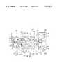
- FIG. 1is a perspective view of an exemplary CMP machine upon which the probe of the present invention is suitably installed;
- FIG. 2is a top view of the CMP machine of FIG. 1, showing an exemplary orientation of the probe assemblies of the present invention
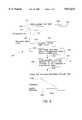
- FIG. 3is a schematic view of a probe in accordance with the present invention configured to sample the surface of a wafer, including a light source, a photospectrum meter, a controller, and a display;
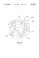
- FIG. 4is an end view of an exemplary bifurcated probe assembly having a plurality of illuminators and a receiver probe;
- FIG. 5is a schematic view of the probe of FIGS. 3 and 4 sampling an individual die structure of a wafer
- FIG. 6is a view of one side of a wafer having a plurality of microelectronic die structures disposed thereon;
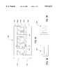
- FIG. 7is a top view of an exemplary embodiment of a wafer carrier lock-in mechanism in accordance with the present invention.
- FIG. 8is a side view of the lock-in mechanism of FIG. 7;
- FIG. 9is a side view of the lock-in mechanism of FIGS. 7 and 8 with a carrier arid wafer assembly in operative engagement with the lock-in mechanism;
- FIG. 10is a cross sectional depiction of an exemplary semiconductor wafer
- FIG. 11is a schematic view of a probe sampling a metallic layer of the semiconductor wafer shown in FIG. 10;
- FIG. 12shows an exemplary output signal generated in response to the sampling of the metallic layer depicted in FIG. 11;
- FIG. 13is a schematic view of a probe sampling an oxide layer of the semiconductor wafer shown in FIG. 10;
- FIG. 14shows an exemplary output signal generated in response to the sampling of the oxide layer depicted in FIG. 13.
- the subject inventionrelates to the in-process detection of characteristics of a layer on a workpiece using a broad spectrum light source, a photospectrum meter, and a controller including a smart algorithm for translating the output of the photospectrum meter to a human readable display relating to the workpiece being examined.
- the preferred embodiment set forth hereinrelates to the detection of oxide layer thickness on a semiconductor wafer (either patterned or non-patterned); it will be appreciated, however, that the principles of the present invention may be employed to ascertain any number of characteristics associated with a workpiece surface, including end point detection, the detection of surface irregularities, planarity, and the like.
- Wafer polishing apparatus 100suitably comprises a multiple head wafer polishing machine which accepts wafers from a previous processing step, polishes and rinses the wafers, and reloads the wafers back into wafer cassettes for subsequent processing.
- apparatus 100comprises an unload station 102, a wafer transition station 104, a polishing station 106, and a wafer rinse and load station 108.
- cassettes 110are loaded into the machine at unload station 102.
- a robotic wafer carrier arm 112removes the wafers from cassettes 110 and places them, one at a time, on first wafer transfer arm 114.
- Wafer transfer arm 114then sequentially lifts and moves each wafer into wafer transition section 104. That is, transfer arm 114 suitably places an individual wafer on one of a plurality of wafer pick-up stations 116 which reside on a rotatable table 120 within wafer transition section 104.
- Rotatable table 120also suitably includes a plurality of wafer drop-off stations 118 which alternate with pick-up stations 116.
- table 120rotates so that a new station 116 aligns with transfer arm 114. Transfer arm 114 then places the next wafer on the new empty pick-up station 116. This process continues until all pick-up stations 116 are filled with wafers.
- table 120includes five pick-up stations 116 and five drop-off stations 118.
- a wafer carrier apparatus 122comprising individual wafer carrier elements 124, suitably aligns itself over table 120 so that respective carrier elements 124 are positioned directly above the wafers which reside in respective pick-up stations 116.
- the carrier apparatus 122then drops down and picks up the wafers from their respective stations and moves the wafers laterally such that the wafers are positioned above polishing station 106.
- carrier apparatus 122suitably lowers the wafers, which are held by individual elements 124, into operative engagement with a polishing pad 126 which sits atop a lap wheel 128.
- lap wheel 128causes polishing pad 126 to rotate about its vertical axis.
- individual carrier elements 124spin the wafers about their respective vertical axes and oscillate the wafers back and forth across pad 126 (substantially along arrow 133) as they press against the polishing pad. In this manner, the undersurface of the wafer is polished or planarized.
- the wafersare removed from polishing pad 126, and carrier apparatus 122 transports the wafers back to transition station 104.
- Carrier apparatus 122then lowers individual carrier elements 124 and deposits the wafers onto drop-off stations 118.
- the wafersare then removed from drop-off stations 118 by a second transfer arm 130.
- Transfer arm 130suitably lifts each wafer out of transition station 104 and transfers them into wafer rinse and load station 108. In the load station 108, transfer arm 130 holds the wafers while they are rinsed. After a thorough rinsing, the wafers are reloaded into cassettes 132, which then transports the subsequent stations for further processing or packaging.
- CMP machine 100is shown having five polishing stations, it will be appreciated that the present invention may be employed in the context of virtually any number polishing stations. Moreover, the present invention may also be employed in circumstances where not all of the polishing stations are functioning at a time. For example, many standard wafer cassettes are capable of carrying up to twenty-five individual workpieces in a single cassette. Consequently, because there are often five workpiece chucks on a single CMP machine, often times the last four disks within a cassette are polished at one time, leaving the fifth disk-holder empty.
- a probe assembly 127is suitably configured near the outer perimeter edge of polishing pad 126 proximate each carrier element 124. More particularly, in a preferred embodiment of the present invention, each respective carrier element suitably oscillates back and forth along arrow 133; each carrier element 124 also suitably rotates a workpiece about the vertical axis of carrier element 124. At the same time, lap wheel 128 and pad 126 are advantageously configured to rotate about their vertical axis, for example, in a counter clockwise direction as indicated by arrow 134.
- each carrier element 124is suitably configured to periodically extend radially outward from the center of table 126 along arrow 125 such that at least a portion of the outside radius of each workpiece extends beyond the outer edge 137 of table 126.
- information relating to surface material thicknesses, desirable material removal rates, and the extent of layer removalmay be obtained for the workpieces.
- the bottom facing surface of the workpiecemay be conveniently optically engaged by probe assembly 127, as described in greater detail below in conjunction with FIG. 3.
- apparatus 100may be configured with a probe assembly 129 useful for detecting the presence of a wafer or wafer fragment on polishing pad 126 during the polishing process.
- the CMP machine 100may be configured to shut down.
- a detailed discussion of the operation of probe assembly 129is discussed in detail in Holzapfel et al., U.S. patent application Ser. No. 08/683,150, filed on Jul. 17, 1996, and entitled Methods and Apparatus for the In-Process Detection of Workpieces in a CMP Environment.
- an exemplary embodiment of probe assembly 127 in accordance with the present inventionsuitably comprises a housing 310 having a nozzle 312 through which compressed air is suitably directed at the undersurface of a workpiece (e.g., semiconductor wafer disk) 306, a bifurcated fiber probe 316, a light source 322, a photospectrum analyzer 324, a controller/processor 326, and a display 328.
- a workpiecee.g., semiconductor wafer disk
- an exemplary workpiece 306is shown being polished by polishing pad 126 as described above in conjunction with FIGS. 1 and 2.
- carrier element 124 and other componentsare omitted from FIG. 3.
- Probe assembly 127is suitably mounted proximate the outer perimeter 330 of pad 126, such that nozzle 312 may be directed at a bottom surface 304 of workpiece 306 when at least a portion of the workpiece extends off the perimeter edge of polishing pad 126.
- a supply of compressed airfor example in the range of 0 to 20 PSI and most preferably about 5 PSI, is urged through housing 310 and nozzle 312 to facilitate the removal of slurry from an exemplary region 314 on undersurface 304 under examination.
- probe 316suitably outputs a broad band (e.g., white light) light source at region 314; a portion of the light emitted by probe 316 is reflected or scattered back from region 314 and captured by probe 316.
- the light output by probe 316suitably passes through a collimating lens 408 which collimates the light (see FIG. 5).
- collimating lens 408is suitably configured to project the light to cover a region 314 on the wafer undersurface that suitably comprises an area in the range of about 10.0 to about 30.0 square millimeters, and preferably about 20.0 square millimeters.
- probe 316suitably comprises a plurality of light illuminators 350 and a single receiver probe 352.
- probe 316preferably comprises a plurality of (e.g. six) illuminators 350 suitably configured around a single receiver probe 352 disposed in the center of the illuminators.
- illuminators 350may suitably be grouped in a hexagonal configuration.
- the diameter of each illuminator 350 and the receiver probe 352, as shown in FIG. 4,is suitably about 100 to about 300 microns and preferably about 200 microns.
- the diameter of probe 316is suitably in the range of 0.1 to 5 millimeters, and preferably about 0.5 to about 2 millimeters, and most preferably about 1 millimeter.
- Probe 316further comprises a transmitter cable 318 through which light is transmitted from light source 322 to illuminators 350 of probe 316 and onto the undersurface of the workpiece.
- probe 316suitably comprises a receptor cable 320 which receives light from receiver probe 350 and transmits it to photospectrum meter 324. It will be appreciated that the undersurface of the workpiece may be sampled by probe assembly 127 at any desired rate or the sampling may be substantially continuous.
- light source 322may suitably comprise any source capable of applying a desired light signal (e.g. broadband, narrow band, or substantially monochromatic) to the surface of the workpiece.
- a desired light signale.g. broadband, narrow band, or substantially monochromatic
- any suitable sourcee.g. a tungsten halogen light source
- a suitable halogen light sourcemay comprise a model number L73A98, available from the Gilway Corporation of Massachausetts.
- cables 318 and 320suitably comprise fiber optic cables in the preferred embodiment, virtually any conductor may be employed which satisfactorily delivers an appropriate signal (e.g. a light signal) to the workpiece and captures at least a portion of the signal reflected by the workpiece.
- an appropriate signale.g. a light signal
- the preferred embodiment set forth hereinemploys a light signal
- virtually any convenient modalitymay be employed to interrogate the surface of the workpiece, e.g., an acoustic signal, magnetic signal, or the like.
- Photospectrum meter 324suitably comprises any circuit capable of interpreting the signal reflected from the undersurface of the workpiece.
- photospectrum meter 324suitably comprises a PCMCIA-based photospectrum meter model number PS1000 available from the Mission Peak Optics Company of Fremont, Calif.
- photospectrum meter 324may be configured as a PC plug-in device, such as model number PC1000 (also available from the Mission Peak Optics Company).
- Controller 326suitably comprises any general purpose controller capable of receiving 30 an output signal 332 from meter 324 and calculating various parameters from signal 332.
- controller 326is suitably configured to interpret signal 332 and thereby derive the thickness of the oxide layer present in region 314 of workpiece 306.
- controller 326suitably comprises any general purpose personal computer, for example a PC, available from the Mission Peaks Optics Company of Fremont, Calif.
- Controller 326is also suitably configured to output a signal 334 to display terminal 328.
- signal 334is indicative of the thickness of the oxide layer at region 314; it will be understood, however, that signal 334 may embody any suitable information or characteristics about surface 304 of the workpiece, such that any number of parameters may be conveniently displayed on the screen associated with display module 328.
- signal 334may convey information indicative of the removal of a first semiconductor layer from a second semiconductor layer (described below). In the embodiment illustrated in FIG. 3, a graph of oxide layer thickness versus time is shown.
- display terminal 328may be suitably configured to display information pertaining to the undersurface of the workpiece. (e.g., the thickness of the oxide layer or the material composition of the exposed layer) in any desired format.
- the remaining processing time necessary to arrive at a desired thickness 340may be visually assessed by the operator; alternatively, controller 326 may be configured to "predict" the time necessary to arrive at a desired thickness for a given pressure and also to display the remaining time to the operator.
- the controllermay be configured to transmit a second output signal 342 to the main controller of machine 100, for example to vary the pressure or other operating parameter(s) associated with the particular carrier element 124 corresponding to the workpiece under inspection.
- controller 326may also be suitably configured to generate a real time or average material removal rate.
- controller 326may suitably be configured to output signal 342 to increase or decrease the removal rate, as desired.
- probe assembly 127may be mounted to machine 100 in any convenient way, for example, by attaching probe assembly 127 to the frame associated with machine 100 by any suitable fastening mechanism. Indeed, it may be possible to dispose respective probe housings 310 quite close to the surface of the workpiece, for example in the range of 0.1 to 0.5 inches and most preferably about 0.3 inches from the workpiece. Even though this environment may be sprayed by slurry droplets from time to time, the compressed air ejected from housing 310 by nozzle 312 suitably substantially prevents slurry from entering the housing and corrupting probe 316.
- One preferred embodiment of an exemplary mounting mechanismis discussed in more detail below in conjunction with FIGS. 7-9.
- probe assembly 127may be suitably configured to output signal 342 to machine 100 to thereby terminate the processing of a particular workpiece when it is determined that desired thickness 340 has been achieved.
- probe assembly 127may be suitably configured to output signal 342 to machine 100 to thereby terminate the processing of a particular workpiece when it is determined that desired thickness 340 has been achieved.
- the need to place partially completed wafers back onto machine 100 for further material removalis substantially eliminated.
- the risk of removing too much of the oxide layer, thus degrading the wafersis also greatly reduced.
- the present inventionmay be alternatively configured to indicate when the oxide layer is initially exposed (described below).
- probe assembly 127samples and interprets the reflected light signals to determine wafer surface thickness will now be described in conjunction with FIGS. 5 and 6.
- an exemplary embodiment of a wafer surfacecomprises a plurality of substantially similar die structures arranged in a rectangular grid pattern.
- each individual die structure 406may comprise in schematic cross section, one or more alternating substrate and oxide layers; for example, a substrate layer 404 and an oxide layer 402.
- Substrate layer 404generally comprises a plurality of microelectronic structures substantially defining a substrate topology 405. Because the surface layer or topology 405 of substrate 404 is non-uniform, it is very difficult to accurately determine the thickness of oxide layer 402 at any particular point on the surface of wafer 400. Therefore, to obtain accurate oxide thickness readings, the effect of the non-uniform substrate surface must be minimized or otherwise accounted for.
- An exemplary wafer surface sampling and analysis method in accordance with the present inventionwill now be discussed in greater detail.
- lightis transmitted from illuminators 350 of probe 316 through collimating lens 408 and onto the undersurface of wafer 400.
- part of the transmitted lightwill be reflected or scattered from oxide layer 402 back to receiver probe 352.
- a substantial portion of the lightpasses through oxide layer 402 and reflects off the substrate layer 404 (and more particularly, the non-uniform surface 405).
- collimating lens 408As the light is reflected off the substrate and oxide layers, it passes back through collimating lens 408, which essentially focuses the reflected light back to receiver probe 352.
- the reflected lightthen passes to photospectrum meter 324 through fiberoptic cable 320.
- Photospectrum meter 324then divides the light into discrete bands of predetermined frequency (or wavelength) ranges and converts the light frequency signals into a digital output signal 332 which is communicated to processor/controller 326.
- processor 326analyses the converted light frequency signals according to the well-known photo-interference technique using Fresnel's Equation to obtain the thickness of the oxide layer at the sampled area of the wafer surface.
- an averaging techniqueis desirably employed which effectively cancels out many of the effects attributable to the complexity of the topography of the wafer.
- an exemplary embodiment of wafer 400comprises a plurality of die structures 406, each comprising substantially similar or identical substrate topologies. Because of the repeating nature of the die structures, the wafer surface may be advantageously sampled for approximately one full wafer rotation, and the measurements taken during that rotation suitably averaged to largely suppress or even cancel out the effects of the non-uniform topology of the dies.
- probe 316suitably collects between about 100 and about 300 samples for one complete rotation, and preferably about 200 samples. Further, one complete rotation of the wafer generally takes approximately 2 seconds; thus, the sampling rate of probe 316 is suitably between about 50 to about 150 samples per second and preferably about 100 samples per second.
- the data for each sampleis transmitted to processor 326 which stores and accumulates the data. After sampling a portion (e.g. region 314) of the wafer for approximately one full wafer rotation, the accumulated data (approximately 200 samples) is averaged and one average oxide thickness is calculated, for example using the aforementioned Fresnel technique. In accordance with a particularly preferred embodiment of the invention, all the sampled data for one rotation is added together and averaged and then the oxide layer thickness is calculated from the averaged data. Alternatively, in accordance with yet another preferred embodiment of the invention, an oxide thickness may be calculated for each individual data sample, and thereafter an average thickness calculated from all the individually calculated thicknesses.
- probe assembly 127and in particular probe 316, is suitably configured to sample the wafer in a substantially circular path 410 (see FIG. 6) so that each die 406 along path 410 is sampled in a substantially uniform manner. That is, because the die structures on the wafer are in a substantially uniform grid pattern and because the field of view of probe 316 suitably corresponds to approximately one die, the probe is likely to sample a complete die structure (as opposed to simply sampling sections of multiple die structures) as it traverses the wafer in a substantially circular pattern.
- a wafer carrier lock-in mechanismmay be used to ensure that the field of view of the probe follows a substantially circular path around the wafer, thus eliminating a spiral reading effect.
- Wafer carrier lock-in mechanism 500will now be discussed in greater detail in conjunction with FIGS. 7-9.
- An exemplary embodiment of wafer lock-in mechanism 500preferably comprises a base 502, a rotatable carrier guide 504, a spring 506 and a stopper 508.
- Rotatable carrier guide 504is suitably mounted to base 502 with a bearing assembly 510 to permit free rotation of guide 504.
- spring 506is suitably mounted between base 502 and stopper 508.
- probe 316is securely mounted within base 502 so that the illuminators and receptor probe are pointed upward toward wafer 400 and wafer carrier element 124.
- wafer carrier 124rotates about its vertical axis and oscillates back and forth across polishing pad 126. As carrier element 124 oscillates across the pad, a portion of the carrier element periodically extends beyond the edge of the pad, contacting rotating carrier guide 504. Carrier guide 504 suitably rotates about bearing 510 as carrier element 124 rotates, thus minimizing friction between the two elements. Once carrier element 124 contacts guide 504, the field of view of probe 316 becomes fixed at a specific radial point on wafer 400. In accordance with this aspect of the invention, as the carrier and wafer assembly rotate, the field of view of the probe traverses a substantially circular path around the wafer ensuring relatively accurate readings.
- the carrierpushes probe 316, guide 504, and base 502 assembly towards stopper 508, compressing spring 506. Then, as the carrier and wafer assembly begin to oscillate back towards the center of polishing pad 126, the tension in spring 506 causes base 502, carrier guide 504, and probe 316 assembly to remain in contact with and to move with the carrier element and wafer, thus maintaining the position of the probe's field of view on the wafer.
- the probemaintains a substantially circular field of view around the wafer as the carrier and wafer rotate and oscillate back and forth across the pad, and therefore, preventing the probe from sampling along a less desirable spiral path on the surface of the wafer.
- the present inventionmay also be employed to detect when a first material layer, e.g., a tungsten or titanium layer, has been removed from a second material layer, e.g., an oxide layer.
- a first material layere.g., a tungsten or titanium layer
- a second material layere.g., an oxide layer.
- the present inventionmay be suitably adapted to detect semiconductor, conductor, or other layers that may be present on a semiconductor wafer. Semiconductor layers are described herein for illustrative purposes only, and the present invention is not limited to the detection of such layers.
- FIG. 10is a cross sectional representation of an exemplary semiconductor wafer 600. Of course, the dimensions of wafer 600 are exaggerated for illustrative purposes.
- Wafer 600may include a silicon substrate base 602, an oxide (silicon dioxide) layer 604, a titanium layer 606, a titanium nitride layer 608, and a tungsten layer 610.
- a number of plugs 611may be formed within wafer 600.
- the metallic upper layerse.g., tungsten layer 610, titanium nitride layer 608, and titanium layer 606, are removed from wafer 600, while some material is maintained within the associated plugs 611. Preferably, material removal terminates (or slows down) when oxide layer 604 is exposed. As described above, the present invention may be employed to measure the thickness of oxide layer 604 to optimize the planarization process.
- a first region 612 of wafer 600may be defined as that portion of wafer 600 above oxide layer 604.
- a second region 614may be defined as that portion of wafer 600 that includes oxide layer 604, silicon base 602, and any other layers (not shown) that may be formed below oxide layer 604. It should be appreciated that although the transition from titanium layer 606 to oxide layer 604 is described herein, the present invention may be suitably adapted to detect the transition from any two material layers having distinguishable optical reflective characteristics. Such adaptation may require additional or alternative processing and/or the application of different detection algorithms than those described above.
- FIG. 11shows probe 316 (see FIGS. 3 and 5) directing an input interrogation signal 616 at wafer 600.
- Input signal 616may be directed toward wafer 600 at an angle of approximately 80 to 100 degrees, and preferably at an angle of approximately 90 degrees, relative to the upper surface 620 of wafer 600.
- the "metallic" layer 618 shown in FIG. 11is intended to generically indicate any semiconductor material of a metallic composition, e.g., tungsten, copper, titanium, titanium or the like. The metallic nature of layer 618 causes input signal 616 to reflect from layer 618.
- FIG. 12depicts an exemplary output 622 that may be generated in response to the continued presence of metallic layer 618 and displayed on display terminal 328 (see FIG. 3 and accompanying discussion).
- a flat output(or any other predetermined display or indicator) may indicate that the reflected signal detected at probe 316 is less than a predetermined threshold value.
- the same outputmay indicate that the reflected signal detected at probe 316 has certain detectable characteristics that are distinguishable from a signal reflected from oxide layer 604.
- the reflected signalitself may have monotonic characteristics when reflected from metallic layer 618 and sinusoidal characteristics when reflected from oxide layer 604 (or a nonmetallic layer).
- wafer polishing apparatus 100may be instructed, by suitable processing and control elements, to continue with the planarization procedure, i.e., to continue removing additional layers or more material from the present layer.
- FIG. 13shows probe 316 directing input signal 616 at wafer 600 after the planarization process has exposed oxide layer 604.
- the metallic layer 618has been removed from wafer 600.
- various plugs 611 formed from tungstenmay remain embedded in oxide layer 604 (see, for example, FIG. 10).
- FIG. 14depicts an exemplary output 624 that may be displayed on display terminal 328 after oxide layer 604 has become exposed.
- a sinusoidal output(or any other predetermined display or indicator) may indicate that the reflected signal detected at probe 316 is greater than the predetermined threshold value.
- the same outputmay indicate that the reflected signal detected at probe 316 has certain detectable characteristics that are distinguishable from a signal reflected from metallic layer 618.
- the reflected signalmay become sinusoidal in nature after the metallic layer 618 has been cleared away and oxide layer 604 becomes the reflective surface.
- suitable control processesmay cause wafer polishing apparatus 100 to halt the planarization procedure or slow the procedure down such that subsequent removal of material may be closely monitored.
- the detection of oxide layer 604 in this manneris substantially independent of the amount and type of slurry and other consumables that may be present in the CMP environment. Unlike conventional endpoint detection techniques that depend on mechanical characteristics such as polishing pad friction and motor currents, the present invention can effectively detect the removal of a metallic layer without relying upon physical interaction with the system. Those skilled in the art will appreciate that the present invention may be utilized to detect the transition between any two reflectively distinguishable materials during a removal or planarization process. For example, if required, the processing and display functions of the present invention may be appropriately modified to detect the removal of an oxide layer from a metallic layer, or one metallic layer from another metallic layer.
- the present inventionprovides improved methods and apparatus for measuring the thickness of layers on semiconductor wafers and other workpiece surfaces.
- the present inventionfacilitates the in-process, in-situ, substantially real time measurement of the actual thickness of a surface layer of a workpiece under inspection.
- a smart algorithmis employed to calculate the thickness of the oxide layer from information gathered from light signals reflected from the surface of the wafer.
- the oxide layer thickness as a function of timeis displayed on a view screen for convenient observation by the operator of the machine.
- the present inventionmay be alternatively configured to optically detect the endpoint when a metallic layer is removed from the oxide layer during the planarization process.
Landscapes
- Engineering & Computer Science (AREA)
- Mechanical Engineering (AREA)
- Manufacturing & Machinery (AREA)
- Computer Hardware Design (AREA)
- Microelectronics & Electronic Packaging (AREA)
- Power Engineering (AREA)
- Physics & Mathematics (AREA)
- General Physics & Mathematics (AREA)
- Testing Or Measuring Of Semiconductors Or The Like (AREA)
- Mechanical Treatment Of Semiconductor (AREA)
Abstract
Description
Claims (17)
Priority Applications (11)
| Application Number | Priority Date | Filing Date | Title |
|---|---|---|---|
| US08/798,803US5872633A (en) | 1996-07-26 | 1997-02-12 | Methods and apparatus for detecting removal of thin film layers during planarization |
| US08/895,284US5958148A (en) | 1996-07-26 | 1997-07-16 | Method for cleaning workpiece surfaces and monitoring probes during workpiece processing |
| PCT/US1997/013373WO1998005066A2 (en) | 1996-07-26 | 1997-07-23 | Methods and apparatus for the in-process detection and measurement of thin film layers |
| TW86110571ATW386276B (en) | 1996-07-26 | 1997-07-25 | Methods and apparatus for the in-process detection and measurement of thin film layers |
| JP10535011AJP2000514251A (en) | 1997-02-12 | 1998-02-06 | Method and apparatus for cleaning the surface of a workpiece and observing a probe during processing of the workpiece |
| KR1019997007199AKR20000070934A (en) | 1997-02-12 | 1998-02-06 | Method and apparatus for cleaning workpiece surface and monitoring probes during workpiece processing |
| DE19882110TDE19882110T1 (en) | 1997-02-12 | 1998-02-06 | Method and device for cleaning workpiece surfaces and monitoring scanning devices during workpiece treatment |
| GB9918179AGB2337476B (en) | 1997-02-12 | 1998-02-06 | Method and apparatus for cleaning workpiece surfaces and monitoring probes during workpiece processing |
| PCT/US1998/002554WO1998034760A1 (en) | 1997-02-12 | 1998-02-06 | Method and apparatus for cleaning workpiece surfaces and monitoring probes during workpiece processing |
| TW087101821ATW380079B (en) | 1997-02-12 | 1998-02-11 | Method and apparatus for cleaning workpiece surfaces and monitoring probes during workpiece processing |
| US09/345,047US6217410B1 (en) | 1996-07-26 | 1999-06-30 | Apparatus for cleaning workpiece surfaces and monitoring probes during workpiece processing |
Applications Claiming Priority (2)
| Application Number | Priority Date | Filing Date | Title |
|---|---|---|---|
| US68771096A | 1996-07-26 | 1996-07-26 | |
| US08/798,803US5872633A (en) | 1996-07-26 | 1997-02-12 | Methods and apparatus for detecting removal of thin film layers during planarization |
Related Parent Applications (1)
| Application Number | Title | Priority Date | Filing Date |
|---|---|---|---|
| US68771096AContinuation-In-Part | 1996-07-26 | 1996-07-26 |
Related Child Applications (1)
| Application Number | Title | Priority Date | Filing Date |
|---|---|---|---|
| US08/895,284Continuation-In-PartUS5958148A (en) | 1996-07-26 | 1997-07-16 | Method for cleaning workpiece surfaces and monitoring probes during workpiece processing |
Publications (1)
| Publication Number | Publication Date |
|---|---|
| US5872633Atrue US5872633A (en) | 1999-02-16 |
Family
ID=27104067
Family Applications (1)
| Application Number | Title | Priority Date | Filing Date |
|---|---|---|---|
| US08/798,803Expired - LifetimeUS5872633A (en) | 1996-07-26 | 1997-02-12 | Methods and apparatus for detecting removal of thin film layers during planarization |
Country Status (1)
| Country | Link |
|---|---|
| US (1) | US5872633A (en) |
Cited By (190)
| Publication number | Priority date | Publication date | Assignee | Title |
|---|---|---|---|---|
| WO1999034958A1 (en)* | 1998-01-06 | 1999-07-15 | Speedfam Corporation | Wafer polishing with improved end point detection |
| US6024628A (en)* | 1999-01-22 | 2000-02-15 | United Microelectronics Corp. | Method of determining real time removal rate for polishing |
| US6042454A (en)* | 1997-06-04 | 2000-03-28 | Ebara Corporation | System for detecting the endpoint of the polishing of a semiconductor wafer by a semiconductor wafer polisher |
| US6066266A (en)* | 1998-07-08 | 2000-05-23 | Lsi Logic Corporation | In-situ chemical-mechanical polishing slurry formulation for compensation of polish pad degradation |
| US6071177A (en)* | 1999-03-30 | 2000-06-06 | Taiwan Semiconductor Manufacturing Co., Ltd | Method and apparatus for determining end point in a polishing process |
| US6106662A (en)* | 1998-06-08 | 2000-08-22 | Speedfam-Ipec Corporation | Method and apparatus for endpoint detection for chemical mechanical polishing |
| WO2000054325A1 (en)* | 1999-03-10 | 2000-09-14 | Nova Measuring Instruments Ltd. | Method and apparatus for monitoring a chemical mechanical planarization process applied to metal-based patterned objects |
| WO2000054935A1 (en)* | 1999-03-18 | 2000-09-21 | Speedfam-Ipec Corporation | Method and apparatus for endpoint detection for chemical mechanical polishing |
| WO2000058716A1 (en)* | 1999-03-26 | 2000-10-05 | Speedfam-Ipec Corporation | Optical endpoint detection system for rotational chemical mechanical polishing |
| US6132289A (en)* | 1998-03-31 | 2000-10-17 | Lam Research Corporation | Apparatus and method for film thickness measurement integrated into a wafer load/unload unit |
| US6142855A (en)* | 1997-10-31 | 2000-11-07 | Canon Kabushiki Kaisha | Polishing apparatus and polishing method |
| WO2000067951A1 (en)* | 1999-05-10 | 2000-11-16 | Speedfam-Ipec Corporation | Optical endpoint detection during chemical mechanical planarization |
| US6159073A (en)* | 1998-11-02 | 2000-12-12 | Applied Materials, Inc. | Method and apparatus for measuring substrate layer thickness during chemical mechanical polishing |
| US6179709B1 (en) | 1999-02-04 | 2001-01-30 | Applied Materials, Inc. | In-situ monitoring of linear substrate polishing operations |
| US6190234B1 (en) | 1999-01-25 | 2001-02-20 | Applied Materials, Inc. | Endpoint detection with light beams of different wavelengths |
| WO2001032363A1 (en)* | 1999-11-03 | 2001-05-10 | Memc Electronic Materials, Inc. | Method of determining performance characteristics of polishing pads |
| WO2001042866A1 (en)* | 1999-12-06 | 2001-06-14 | Nova Measuring Instruments Ltd. | Method and system for endpoint detection |
| US6247998B1 (en) | 1999-01-25 | 2001-06-19 | Applied Materials, Inc. | Method and apparatus for determining substrate layer thickness during chemical mechanical polishing |
| WO2001056744A1 (en)* | 2000-02-01 | 2001-08-09 | Applied Materials, Inc. | Endpoint monitoring with polishing rate change |
| US6280289B1 (en) | 1998-11-02 | 2001-08-28 | Applied Materials, Inc. | Method and apparatus for detecting an end-point in chemical mechanical polishing of metal layers |
| US6292265B1 (en) | 1999-03-10 | 2001-09-18 | Nova Measuring Instruments Ltd. | Method and apparatus for monitoring a chemical mechanical planarization process applied to metal-based patterned objects |
| US6293845B1 (en)* | 1999-09-04 | 2001-09-25 | Mitsubishi Materials Corporation | System and method for end-point detection in a multi-head CMP tool using real-time monitoring of motor current |
| US6293846B1 (en)* | 1997-06-17 | 2001-09-25 | Ebara Corporation | Polishing apparatus |
| US6296548B1 (en) | 1998-11-02 | 2001-10-02 | Applied Materials, Inc. | Method and apparatus for optical monitoring in chemical mechanical polishing |
| US6312320B2 (en) | 1998-06-16 | 2001-11-06 | Kioritz Corporation | Disk cleaner |
| US6319093B1 (en) | 2001-02-06 | 2001-11-20 | International Business Machines Corporation | Chemical-mechanical polishing system and method for integrated spin dry-film thickness measurement |
| US20010044261A1 (en)* | 1999-04-26 | 2001-11-22 | Elledge Jason B. | Apparatus for in-situ optical endpointing on web-format planarizing machines in mechanical or chemical-mechanical planarization of microelectronic-device substrate assemblies and methods for making and using same |
| US6332470B1 (en) | 1997-12-30 | 2001-12-25 | Boris Fishkin | Aerosol substrate cleaner |
| US6334807B1 (en)* | 1999-04-30 | 2002-01-01 | International Business Machines Corporation | Chemical mechanical polishing in-situ end point system |
| WO2002004887A1 (en)* | 2000-07-08 | 2002-01-17 | Semitool, Inc. | Methods and apparatus for processing microelectronic workpieces using metrology |
| WO2002004886A1 (en)* | 2000-07-08 | 2002-01-17 | Semitool, Inc. | Apparatus and method for processing a microelectronic workpiece using metrology |
| US6361411B1 (en)* | 1999-06-21 | 2002-03-26 | Micron Technology, Inc. | Method for conditioning polishing surface |
| US6383058B1 (en) | 2000-01-28 | 2002-05-07 | Applied Materials, Inc. | Adaptive endpoint detection for chemical mechanical polishing |
| US6399501B2 (en)* | 1999-12-13 | 2002-06-04 | Applied Materials, Inc. | Method and apparatus for detecting polishing endpoint with optical monitoring |
| US6406641B1 (en)* | 1997-06-17 | 2002-06-18 | Luxtron Corporation | Liquid etch endpoint detection and process metrology |
| US20020103564A1 (en)* | 2000-09-20 | 2002-08-01 | John Fielden | Methods and systems for determining a composition and a thickness of a specimen |
| US6428673B1 (en) | 2000-07-08 | 2002-08-06 | Semitool, Inc. | Apparatus and method for electrochemical processing of a microelectronic workpiece, capable of modifying processing based on metrology |
| US20020107650A1 (en)* | 2000-09-20 | 2002-08-08 | Dan Wack | Methods and systems for determining a critical dimension and a presence of defects on a specimen |
| US20020106848A1 (en)* | 2000-09-20 | 2002-08-08 | Dan Wack | Methods and systems for determining a property of a specimen prior to, during, or subsequent to lithography |
| US6433541B1 (en) | 1999-12-23 | 2002-08-13 | Kla-Tencor Corporation | In-situ metalization monitoring using eddy current measurements during the process for removing the film |
| WO2002033737A3 (en)* | 2000-10-17 | 2002-08-15 | Speedfam Ipec Corp | Multiprobe detection system for chemical-mechanical planarization tool |
| WO2002031866A3 (en)* | 2000-10-13 | 2002-09-06 | Lam Res Corp | Infrared end-point system for cmp |
| US6491569B2 (en) | 2001-04-19 | 2002-12-10 | Speedfam-Ipec Corporation | Method and apparatus for using optical reflection data to obtain a continuous predictive signal during CMP |
| US20020192966A1 (en)* | 2001-06-19 | 2002-12-19 | Shanmugasundram Arulkumar P. | In situ sensor based control of semiconductor processing procedure |
| US6506097B1 (en) | 2000-01-18 | 2003-01-14 | Applied Materials, Inc. | Optical monitoring in a two-step chemical mechanical polishing process |
| US6514775B2 (en) | 2001-06-29 | 2003-02-04 | Kla-Tencor Technologies Corporation | In-situ end point detection for semiconductor wafer polishing |
| US6524164B1 (en) | 1999-09-14 | 2003-02-25 | Applied Materials, Inc. | Polishing pad with transparent window having reduced window leakage for a chemical mechanical polishing apparatus |
| US20030038035A1 (en)* | 2001-05-30 | 2003-02-27 | Wilson Gregory J. | Methods and systems for controlling current in electrochemical processing of microelectronic workpieces |
| US20030045008A1 (en)* | 2001-08-31 | 2003-03-06 | Gregory Olsen | Method and apparatus for monitoring changes in the surface of a workpiece during processing |
| US6537134B2 (en) | 2000-10-06 | 2003-03-25 | Cabot Microelectronics Corporation | Polishing pad comprising a filled translucent region |
| US20030070918A1 (en)* | 2001-08-31 | 2003-04-17 | Hanson Kyle M. | Apparatus and methods for electrochemical processing of microelectronic workpieces |
| US20030086097A1 (en)* | 2001-09-30 | 2003-05-08 | Nova Measuring Instruments Ltd. | Method and system for thin film characterization |
| US6570662B1 (en) | 1999-05-24 | 2003-05-27 | Luxtron Corporation | Optical techniques for measuring layer thicknesses and other surface characteristics of objects such as semiconductor wafers |
| US6572445B2 (en) | 2001-05-16 | 2003-06-03 | Speedfam-Ipec | Multizone slurry delivery for chemical mechanical polishing tool |
| US6579149B2 (en) | 2001-02-06 | 2003-06-17 | International Business Machines Corporation | Support and alignment device for enabling chemical mechanical polishing rinse and film measurements |
| US20030127337A1 (en)* | 1999-04-13 | 2003-07-10 | Hanson Kayle M. | Apparatus and methods for electrochemical processing of microelectronic workpieces |
| US6602724B2 (en) | 2000-07-27 | 2003-08-05 | Applied Materials, Inc. | Chemical mechanical polishing of a metal layer with polishing rate monitoring |
| WO2002052637A3 (en)* | 2000-12-27 | 2003-08-14 | Lam Res Corp | Method and apparatus for monitoring a semiconductor wafer during a spin drying operation |
| US20030180973A1 (en)* | 2002-02-04 | 2003-09-25 | Kurt Lehman | Methods and systems for monitoring a parameter of a measurement device during polishing, damage to a specimen during polishing, or a characteristic of a polishing pad or tool |
| US6628397B1 (en) | 1999-09-15 | 2003-09-30 | Kla-Tencor | Apparatus and methods for performing self-clearing optical measurements |
| US6634924B1 (en) | 1999-09-28 | 2003-10-21 | Ebara Corporation | Polishing apparatus |
| US20030216104A1 (en)* | 2002-05-16 | 2003-11-20 | Nikolay Korovin | Method for processing a work piece in a multi-zonal processing apparatus |
| US6652366B2 (en) | 2001-05-16 | 2003-11-25 | Speedfam-Ipec Corporation | Dynamic slurry distribution control for CMP |
| US6671051B1 (en) | 1999-09-15 | 2003-12-30 | Kla-Tencor | Apparatus and methods for detecting killer particles during chemical mechanical polishing |
| US6673637B2 (en) | 2000-09-20 | 2004-01-06 | Kla-Tencor Technologies | Methods and systems for determining a presence of macro defects and overlay of a specimen |
| US6676482B2 (en) | 2001-04-20 | 2004-01-13 | Speedfam-Ipec Corporation | Learning method and apparatus for predictive determination of endpoint during chemical mechanical planarization using sparse sampling |
| US6694284B1 (en) | 2000-09-20 | 2004-02-17 | Kla-Tencor Technologies Corp. | Methods and systems for determining at least four properties of a specimen |
| US20040033758A1 (en)* | 2001-12-28 | 2004-02-19 | Wiswesser Andreas Norbert | Polishing pad with window |
| US6707540B1 (en) | 1999-12-23 | 2004-03-16 | Kla-Tencor Corporation | In-situ metalization monitoring using eddy current and optical measurements |
| US20040055877A1 (en)* | 1999-04-13 | 2004-03-25 | Wilson Gregory J. | Workpiece processor having processing chamber with improved processing fluid flow |
| DE10241155A1 (en)* | 2002-09-05 | 2004-03-25 | Infineon Technologies Ag | Device for finishing thinning of a workpiece used in the production of integrated circuits and transistors comprises a radiation emitting unit which directs radiation onto a region, a radiation receiving unit, and an evaluation unit |
| US6716085B2 (en) | 2001-12-28 | 2004-04-06 | Applied Materials Inc. | Polishing pad with transparent window |
| US6720568B2 (en) | 2000-08-31 | 2004-04-13 | Nova Measuring Instruments Ltd. | Method and system for optical inspection of a structure formed with a surface relief |
| US20040082271A1 (en)* | 1999-01-25 | 2004-04-29 | Wiswesser Andreas Norbert | Polishing pad with window |
| US20040108212A1 (en)* | 2002-12-06 | 2004-06-10 | Lyndon Graham | Apparatus and methods for transferring heat during chemical processing of microelectronic workpieces |
| US6812045B1 (en) | 2000-09-20 | 2004-11-02 | Kla-Tencor, Inc. | Methods and systems for determining a characteristic of a specimen prior to, during, or subsequent to ion implantation |
| US6821794B2 (en) | 2001-10-04 | 2004-11-23 | Novellus Systems, Inc. | Flexible snapshot in endpoint detection |
| US20040235205A1 (en)* | 2000-09-20 | 2004-11-25 | Kla-Tencor, Inc. | Methods and systems for determining a critical dimension and overlay of a specimen |
| US20040259472A1 (en)* | 2003-04-01 | 2004-12-23 | Chalmers Scott A. | Whole-substrate spectral imaging system for CMP |
| US20050048874A1 (en)* | 2001-12-28 | 2005-03-03 | Applied Materials, Inc., A Delaware Corporation | System and method for in-line metal profile measurement |
| US20050061676A1 (en)* | 2001-03-12 | 2005-03-24 | Wilson Gregory J. | System for electrochemically processing a workpiece |
| US6878038B2 (en) | 2000-07-10 | 2005-04-12 | Applied Materials Inc. | Combined eddy current sensing and optical monitoring for chemical mechanical polishing |
| US20050088647A1 (en)* | 2003-09-19 | 2005-04-28 | Applied Materials, Inc. | Apparatus and method of detecting the electroless deposition endpoint |
| US20050105103A1 (en)* | 1999-05-24 | 2005-05-19 | Luxtron Corporation | Optical techniques for measuring layer thicknesses and other surface characteristics of objects such as semiconductor wafers |
| US20050128490A1 (en)* | 1999-02-01 | 2005-06-16 | Stanke Fred E. | Apparatus for imaging metrology |
| US20050153634A1 (en)* | 2004-01-09 | 2005-07-14 | Cabot Microelectronics Corporation | Negative poisson's ratio material-containing CMP polishing pad |
| US6919957B2 (en) | 2000-09-20 | 2005-07-19 | Kla-Tencor Technologies Corp. | Methods and systems for determining a critical dimension, a presence of defects, and a thin film characteristic of a specimen |
| US20050155864A1 (en)* | 1999-04-13 | 2005-07-21 | Woodruff Daniel J. | Adaptable electrochemical processing chamber |
| US20050161336A1 (en)* | 1998-07-10 | 2005-07-28 | Woodruff Daniel J. | Electroplating apparatus with segmented anode array |
| US20050167274A1 (en)* | 1999-04-13 | 2005-08-04 | Wilson Gregory J. | Tuning electrodes used in a reactor for electrochemically processing a microelectronics workpiece |
| US20050183959A1 (en)* | 2000-04-13 | 2005-08-25 | Wilson Gregory J. | Tuning electrodes used in a reactor for electrochemically processing a microelectric workpiece |
| US20050189215A1 (en)* | 1999-04-13 | 2005-09-01 | Hanson Kyle M. | Apparatus and methods for electrochemical processing of microelectronic workpieces |
| US20050211376A1 (en)* | 2004-03-25 | 2005-09-29 | Cabot Microelectronics Corporation | Polishing pad comprising hydrophobic region and endpoint detection port |
| US20050221723A1 (en)* | 2003-10-03 | 2005-10-06 | Applied Materials, Inc. | Multi-layer polishing pad for low-pressure polishing |
| US6966816B2 (en) | 2001-05-02 | 2005-11-22 | Applied Materials, Inc. | Integrated endpoint detection system with optical and eddy current monitoring |
| US20060000716A1 (en)* | 1999-04-13 | 2006-01-05 | Wilson Gregory J | Tuning electrodes used in a reactor for electrochemically processing a microelectronic workpiece |
| US20060020419A1 (en)* | 2004-07-22 | 2006-01-26 | Applied Materials, Inc. | Iso-reflectance wavelengths |
| EP1322940A4 (en)* | 2000-07-31 | 2006-03-15 | Asml Us Inc | METHOD AND IN SITU DEVICE FOR DETECTING THE TURN POINT FOR CHEMICAL MECHANICAL POLISHING |
| US20060062897A1 (en)* | 2004-09-17 | 2006-03-23 | Applied Materials, Inc | Patterned wafer thickness detection system |
| US20060076317A1 (en)* | 2004-10-12 | 2006-04-13 | Cabot Microelectronics Corporation | CMP composition with a polymer additive for polishing noble metals |
| US7042580B1 (en)* | 1999-02-01 | 2006-05-09 | Tokyo Electron Limited | Apparatus for imaging metrology |
| US7042558B1 (en) | 2001-03-19 | 2006-05-09 | Applied Materials | Eddy-optic sensor for object inspection |
| US20060099814A1 (en)* | 2004-11-05 | 2006-05-11 | Cabot Microelectronics Corporation | Polishing composition and method for high silicon nitride to silicon oxide removal rate ratios |
| US20060096496A1 (en)* | 2004-10-28 | 2006-05-11 | Cabot Microelectronic Corporation | CMP composition comprising surfactant |
| US20060096179A1 (en)* | 2004-11-05 | 2006-05-11 | Cabot Microelectronics Corporation | CMP composition containing surface-modified abrasive particles |
| US20060108326A1 (en)* | 2004-11-05 | 2006-05-25 | Cabot Microelectronics | Polishing composition and method for high silicon nitride to silicon oxide removal rate ratios |
| US7096752B1 (en) | 2004-11-02 | 2006-08-29 | Kla-Tencor Technologies Corporation | Environmental damage reduction |
| US7097537B1 (en) | 2003-08-18 | 2006-08-29 | Applied Materials, Inc. | Determination of position of sensor measurements during polishing |
| US7106425B1 (en) | 2000-09-20 | 2006-09-12 | Kla-Tencor Technologies Corp. | Methods and systems for determining a presence of defects and a thin film characteristic of a specimen |
| US20060226126A1 (en)* | 2005-03-30 | 2006-10-12 | Cabot Microelectronics Corporation | Polymeric inhibitors for enhanced planarization |
| US7130029B2 (en) | 2000-09-20 | 2006-10-31 | Kla-Tencor Technologies Corp. | Methods and systems for determining an adhesion characteristic and a thickness of a specimen |
| US20060286906A1 (en)* | 2005-06-21 | 2006-12-21 | Cabot Microelectronics Corporation | Polishing pad comprising magnetically sensitive particles and method for the use thereof |
| US7153185B1 (en) | 2003-08-18 | 2006-12-26 | Applied Materials, Inc. | Substrate edge detection |
| US20070010098A1 (en)* | 2005-06-30 | 2007-01-11 | Cabot Microelectronics Corporation | Use of CMP for aluminum mirror and solar cell fabrication |
| US7195535B1 (en) | 2004-07-22 | 2007-03-27 | Applied Materials, Inc. | Metrology for chemical mechanical polishing |
| US7253078B1 (en) | 1999-07-22 | 2007-08-07 | National Semiconductor Corporation | Method and apparatus for forming an underfill adhesive layer |
| US20070209287A1 (en)* | 2006-03-13 | 2007-09-13 | Cabot Microelectronics Corporation | Composition and method to polish silicon nitride |
| US20070221502A1 (en)* | 1999-04-13 | 2007-09-27 | Semitool, Inc. | Tuning electrodes used in a reactor for electrochemically processing a microelectronic workpiece |
| US20070224822A1 (en)* | 2006-03-23 | 2007-09-27 | Cabot Microelectronics Corporation | Halide anions for metal removal rate control |
| US20070224919A1 (en)* | 2006-03-23 | 2007-09-27 | Cabot Microelectronics Corporation | Iodate-containing chemical-mechanical polishing compositions and methods |
| US7282375B1 (en) | 2004-04-14 | 2007-10-16 | National Semiconductor Corporation | Wafer level package design that facilitates trimming and testing |
| US20070249167A1 (en)* | 2006-04-21 | 2007-10-25 | Cabot Microelectronics Corporation | CMP method for copper-containing substrates |
| US20070254557A1 (en)* | 2002-10-17 | 2007-11-01 | Yoichi Kobayashi | Polishing state monitoring apparatus and polishing apparatus and method |
| US20070251155A1 (en)* | 2006-04-27 | 2007-11-01 | Cabot Microelectronics Corporation | Polishing composition containing polyether amine |
| US7294576B1 (en) | 2006-06-29 | 2007-11-13 | Cabot Microelectronics Corporation | Tunable selectivity slurries in CMP applications |
| US7301222B1 (en) | 2003-02-12 | 2007-11-27 | National Semiconductor Corporation | Apparatus for forming a pre-applied underfill adhesive layer for semiconductor wafer level chip-scale packages |
| US20070298612A1 (en)* | 2006-06-07 | 2007-12-27 | Jeffrey Dysard | Compositions and methods for polishing silicon nitride materials |
| US20080020577A1 (en)* | 2006-07-21 | 2008-01-24 | Cabot Microelectronics Corporation | Gallium and chromium ions for oxide rate enhancement |
| US20080057715A1 (en)* | 2006-08-30 | 2008-03-06 | Cabot Microelectronics Corporation | Cmp system utilizing halogen adduct |
| US20080096390A1 (en)* | 2006-03-23 | 2008-04-24 | Cabot Microelectronics Corporation | Halide anions for metal removal rate control |
| US20080105652A1 (en)* | 2006-11-02 | 2008-05-08 | Cabot Microelectronics Corporation | CMP of copper/ruthenium/tantalum substrates |
| US20080113589A1 (en)* | 2006-11-13 | 2008-05-15 | Cabot Microelectronics Corporation | Composition and method for damascene CMP |
| US20080134585A1 (en)* | 2006-12-06 | 2008-06-12 | Cabot Microelectronics Corporation | Compositions for polishing aluminum/copper and titanium in damascene structures |
| US7423337B1 (en) | 2002-08-19 | 2008-09-09 | National Semiconductor Corporation | Integrated circuit device package having a support coating for improved reliability during temperature cycling |
| US20080220610A1 (en)* | 2006-06-29 | 2008-09-11 | Cabot Microelectronics Corporation | Silicon oxide polishing method utilizing colloidal silica |
| EP2025469A1 (en) | 2003-06-17 | 2009-02-18 | Cabot Microelectronics Corporation | Multi-layer polishing pad material for CMP |
| US20090081871A1 (en)* | 2007-09-21 | 2009-03-26 | Cabot Microelectronics Corporation | Polishing composition and method utilizing abrasive particles treated with an aminosilane |
| US20090081927A1 (en)* | 2007-09-21 | 2009-03-26 | Cabot Microelectronics Corporation | Polishing composition and method utilizing abrasive particles treated with an aminosilane |
| US20090149115A1 (en)* | 2007-09-24 | 2009-06-11 | Ignacio Palou-Rivera | Wafer edge characterization by successive radius measurements |
| WO2009142692A2 (en) | 2008-05-23 | 2009-11-26 | Cabot Microelectronics Corporation | Stable, high rate silicon slurry |
| WO2010033156A2 (en) | 2008-09-19 | 2010-03-25 | Cabot Microelectronics Corporation | Barrier slurry for low-k dielectrics |
| US20110062115A1 (en)* | 2009-09-16 | 2011-03-17 | Cabot Microelectronics Corporation | Composition and method for polishing bulk silicon |
| US20110062376A1 (en)* | 2009-09-16 | 2011-03-17 | Brian Reiss | Composition and method for polishing bulk silicon |
| US20110136344A1 (en)* | 2009-09-16 | 2011-06-09 | Cabot Microelectronics Corporation | Composition and method for polishing polysilicon |
| WO2011088057A1 (en) | 2010-01-13 | 2011-07-21 | Nexplanar Corporation | Cmp pad with local area transparency |
| EP2431434A1 (en) | 2004-07-28 | 2012-03-21 | Cabot Microelectronics Corporation | Polishing Composition for Noble Metals |
| CN101966687B (en)* | 2009-07-27 | 2012-11-28 | 中芯国际集成电路制造(上海)有限公司 | Chemical mechanical lapping method |
| WO2013138558A1 (en) | 2012-03-14 | 2013-09-19 | Cabot Microelectronics Corporation | Cmp compositions selective for oxide and nitride with high removal rate and low defectivity |
| WO2013177110A1 (en) | 2012-05-22 | 2013-11-28 | Cabot Microelectronics Corporation | Cmp composition containing zirconia particles and method of use |
| WO2014120541A1 (en) | 2013-01-30 | 2014-08-07 | Cabot Microelectronics Corporation | Chemical-mechanical polishing composition containing zirconia and metal oxidizer |
| US20140242877A1 (en)* | 2013-02-26 | 2014-08-28 | Applied Materials, Inc. | Spectrographic metrology with multiple measurements |
| US8821215B2 (en) | 2012-09-07 | 2014-09-02 | Cabot Microelectronics Corporation | Polypyrrolidone polishing composition and method |
| US8906252B1 (en) | 2013-05-21 | 2014-12-09 | Cabot Microelelctronics Corporation | CMP compositions selective for oxide and nitride with high removal rate and low defectivity |
| US8916061B2 (en) | 2012-03-14 | 2014-12-23 | Cabot Microelectronics Corporation | CMP compositions selective for oxide and nitride with high removal rate and low defectivity |
| US8961807B2 (en) | 2013-03-15 | 2015-02-24 | Cabot Microelectronics Corporation | CMP compositions with low solids content and methods related thereto |
| WO2015053985A1 (en) | 2013-10-10 | 2015-04-16 | Cabot Microelectronics Corporation | Mixed abrasive polishing compositions |
| WO2015053982A1 (en) | 2013-10-10 | 2015-04-16 | Cabot Microelectronics Corporation | Wet process ceria compositions for polishing substrates, and methods related thereto |
| US9039914B2 (en) | 2012-05-23 | 2015-05-26 | Cabot Microelectronics Corporation | Polishing composition for nickel-phosphorous-coated memory disks |
| US9165489B2 (en) | 2013-05-21 | 2015-10-20 | Cabot Microelectronics Corporation | CMP compositions selective for oxide over polysilicon and nitride with high removal rate and low defectivity |
| WO2015171419A1 (en) | 2014-05-07 | 2015-11-12 | Cabot Microelectronics Corporation | Multi-layer polishing pad for cmp |
| US20150355416A1 (en)* | 2014-06-06 | 2015-12-10 | Corning Optical Communications LLC | Methods and systems for polishing optical fibers |
| US9279067B2 (en) | 2013-10-10 | 2016-03-08 | Cabot Microelectronics Corporation | Wet-process ceria compositions for polishing substrates, and methods related thereto |
| WO2016065057A1 (en) | 2014-10-21 | 2016-04-28 | Cabot Microelectronics Corporation | Corrosion inhibitors and related compositions and methods |
| WO2016073181A1 (en)* | 2014-11-04 | 2016-05-12 | Headway Technologies, Inc. | Method for adaptive feedback controlled polishing |
| US9358659B2 (en) | 2013-03-04 | 2016-06-07 | Cabot Microelectronics Corporation | Composition and method for polishing glass |
| WO2016094028A1 (en) | 2014-12-12 | 2016-06-16 | Cabot Microelectronics Corporation | Cmp compositons exhibiting reduced dishing in sti wafer polishing |
| US9401104B2 (en) | 2014-05-05 | 2016-07-26 | Cabot Microelectronics Corporation | Polishing composition for edge roll-off improvement |
| WO2016126458A1 (en) | 2015-02-03 | 2016-08-11 | Cabot Microelectronics Corporation | Cmp composition for silicon nitride removal |
| US9434859B2 (en) | 2013-09-24 | 2016-09-06 | Cabot Microelectronics Corporation | Chemical-mechanical planarization of polymer films |
| WO2016140968A1 (en) | 2015-03-05 | 2016-09-09 | Cabot Microelectronics Corporation | Polishing composition containing ceria abrasive |
| WO2017011451A1 (en) | 2015-07-13 | 2017-01-19 | Cabot Microelectronics Corporation | Methods and compositions for processing dielectric substrate |
| WO2017070074A1 (en) | 2015-10-21 | 2017-04-27 | Cabot Microelectronics Corporation | Cobalt inhibitor combination for improved dishing |
| US9688885B2 (en) | 2014-10-21 | 2017-06-27 | Cabot Microelectronics Corporation | Cobalt polishing accelerators |
| WO2017120396A1 (en) | 2016-01-06 | 2017-07-13 | Cabot Microelectronics Corporation | Method of polishing a low-k substrate |
| US9834704B2 (en) | 2014-10-21 | 2017-12-05 | Cabot Microelectronics Corporation | Cobalt dishing control agents |
| WO2018013847A1 (en) | 2016-07-14 | 2018-01-18 | Cabot Microelectronics Corporation | Alternative oxidizing agents for cobalt cmp |
| US9909032B2 (en) | 2014-01-15 | 2018-03-06 | Cabot Microelectronics Corporation | Composition and method for polishing memory hard disks |
| US9944828B2 (en) | 2014-10-21 | 2018-04-17 | Cabot Microelectronics Corporation | Slurry for chemical mechanical polishing of cobalt |
| WO2018128849A1 (en) | 2017-01-05 | 2018-07-12 | Cabot Microelectronics Corporation | Composition and method for polishing silicon carbide |
| WO2019055160A2 (en) | 2017-09-15 | 2019-03-21 | Cabot Microelectronics Corporation | Nitride inhibitors for high selectivity of tin-sin cmp applications |
| WO2019070793A1 (en) | 2017-10-03 | 2019-04-11 | Cabot Microelectronics Corporation | Surface treated abrasive particles for tungsten buff applications |
| US10414947B2 (en) | 2015-03-05 | 2019-09-17 | Cabot Microelectronics Corporation | Polishing composition containing ceria particles and method of use |
| WO2020214662A1 (en) | 2019-04-17 | 2020-10-22 | Cabot Microelectronics Corporation | Surface coated abrasive particles for tungsten buff applications |
| WO2021011196A1 (en) | 2019-07-16 | 2021-01-21 | Cabot Microelectronics Corporation | Method to increase barrier film removal rate in bulk tungsten slurry |
| US10898986B2 (en) | 2017-09-15 | 2021-01-26 | Applied Materials, Inc. | Chattering correction for accurate sensor position determination on wafer |
| CN115077387A (en)* | 2022-08-22 | 2022-09-20 | 成都岁生科技有限责任公司 | Wedge detection method based on point cloud technology |
| US20230184533A1 (en)* | 2020-08-25 | 2023-06-15 | Corning Incorporated | In-situ deposition thickness monitoring |
| CN118658835A (en)* | 2024-08-14 | 2024-09-17 | 合肥晶合集成电路股份有限公司 | Method for manufacturing semiconductor device, semiconductor device and test method |
| US12227673B2 (en) | 2018-12-04 | 2025-02-18 | Cmc Materials Llc | Composition and method for silicon nitride CMP |
| US12269969B2 (en) | 2019-10-22 | 2025-04-08 | Cmc Materials Llc | Polishing composition and method with high selectivity for silicon nitride and polysilicon over silicon oxide |
Citations (21)
| Publication number | Priority date | Publication date | Assignee | Title |
|---|---|---|---|---|
| US4462860A (en)* | 1982-05-24 | 1984-07-31 | At&T Bell Laboratories | End point detection |
| US4805348A (en)* | 1985-07-31 | 1989-02-21 | Speedfam Co., Ltd. | Flat lapping machine |
| US5099614A (en)* | 1986-09-01 | 1992-03-31 | Speedfam Co., Ltd. | Flat lapping machine with sizing mechanism |
| US5240552A (en)* | 1991-12-11 | 1993-08-31 | Micron Technology, Inc. | Chemical mechanical planarization (CMP) of a semiconductor wafer using acoustical waves for in-situ end point detection |
| USRE34425E (en)* | 1990-08-06 | 1993-11-02 | Micron Technology, Inc. | Method and apparatus for mechanical planarization and endpoint detection of a semiconductor wafer |
| US5329732A (en)* | 1992-06-15 | 1994-07-19 | Speedfam Corporation | Wafer polishing method and apparatus |
| EP0663265A1 (en)* | 1993-12-22 | 1995-07-19 | International Business Machines Corporation | In-situ endpoint detection and process monitoring method and apparatus for chemical-mechanical polishing |
| US5486129A (en)* | 1993-08-25 | 1996-01-23 | Micron Technology, Inc. | System and method for real-time control of semiconductor a wafer polishing, and a polishing head |
| US5486701A (en)* | 1992-06-16 | 1996-01-23 | Prometrix Corporation | Method and apparatus for measuring reflectance in two wavelength bands to enable determination of thin film thickness |
| US5498199A (en)* | 1992-06-15 | 1996-03-12 | Speedfam Corporation | Wafer polishing method and apparatus |
| WO1996016436A1 (en)* | 1994-11-18 | 1996-05-30 | Advanced Micro Devices, Inc. | Method of making a chemical-mechanical polishing slurry and the polishing slurry |
| EP0718595A2 (en)* | 1994-12-21 | 1996-06-26 | Hughes Aircraft Company | Automatic rejection of diffraction effects in thin film metrology |
| US5543919A (en)* | 1993-05-14 | 1996-08-06 | Integrated Process Equipment Corp. | Apparatus and method for performing high spatial resolution thin film layer thickness metrology |
| US5555472A (en)* | 1993-12-22 | 1996-09-10 | Integrated Process Equipment Corp. | Method and apparatus for measuring film thickness in multilayer thin film stack by comparison to a reference library of theoretical signatures |
| US5559428A (en)* | 1995-04-10 | 1996-09-24 | International Business Machines Corporation | In-situ monitoring of the change in thickness of films |
| US5562529A (en)* | 1992-10-08 | 1996-10-08 | Fujitsu Limited | Apparatus and method for uniformly polishing a wafer |
| US5568252A (en)* | 1993-12-28 | 1996-10-22 | Dainippon Screen Manufacturing Co., Ltd. | Method and apparatus for measuring insulation film thickness of semiconductor wafer |
| EP0738561A1 (en)* | 1995-03-28 | 1996-10-23 | Applied Materials, Inc. | Apparatus and method for in-situ endpoint detection and monitoring for chemical mechanical polishing operations |
| US5609511A (en)* | 1994-04-14 | 1997-03-11 | Hitachi, Ltd. | Polishing method |
| JPH09159409A (en)* | 1995-12-07 | 1997-06-20 | Dainippon Screen Mfg Co Ltd | Surface treatment end point detector |
| EP0806266A2 (en)* | 1996-05-09 | 1997-11-12 | Canon Kabushiki Kaisha | Polishing method and polishing apparatus using the same |
- 1997
- 1997-02-12USUS08/798,803patent/US5872633A/ennot_activeExpired - Lifetime
Patent Citations (23)
| Publication number | Priority date | Publication date | Assignee | Title |
|---|---|---|---|---|
| US4462860A (en)* | 1982-05-24 | 1984-07-31 | At&T Bell Laboratories | End point detection |
| US4805348A (en)* | 1985-07-31 | 1989-02-21 | Speedfam Co., Ltd. | Flat lapping machine |
| US5099614A (en)* | 1986-09-01 | 1992-03-31 | Speedfam Co., Ltd. | Flat lapping machine with sizing mechanism |
| USRE34425E (en)* | 1990-08-06 | 1993-11-02 | Micron Technology, Inc. | Method and apparatus for mechanical planarization and endpoint detection of a semiconductor wafer |
| US5240552A (en)* | 1991-12-11 | 1993-08-31 | Micron Technology, Inc. | Chemical mechanical planarization (CMP) of a semiconductor wafer using acoustical waves for in-situ end point detection |
| US5498196A (en)* | 1992-06-15 | 1996-03-12 | Speedfam Corporation | Wafer polishing method and apparatus |
| US5498199A (en)* | 1992-06-15 | 1996-03-12 | Speedfam Corporation | Wafer polishing method and apparatus |
| US5329732A (en)* | 1992-06-15 | 1994-07-19 | Speedfam Corporation | Wafer polishing method and apparatus |
| US5486701A (en)* | 1992-06-16 | 1996-01-23 | Prometrix Corporation | Method and apparatus for measuring reflectance in two wavelength bands to enable determination of thin film thickness |
| US5562529A (en)* | 1992-10-08 | 1996-10-08 | Fujitsu Limited | Apparatus and method for uniformly polishing a wafer |
| US5543919A (en)* | 1993-05-14 | 1996-08-06 | Integrated Process Equipment Corp. | Apparatus and method for performing high spatial resolution thin film layer thickness metrology |
| US5486129A (en)* | 1993-08-25 | 1996-01-23 | Micron Technology, Inc. | System and method for real-time control of semiconductor a wafer polishing, and a polishing head |
| US5555472A (en)* | 1993-12-22 | 1996-09-10 | Integrated Process Equipment Corp. | Method and apparatus for measuring film thickness in multilayer thin film stack by comparison to a reference library of theoretical signatures |
| EP0663265A1 (en)* | 1993-12-22 | 1995-07-19 | International Business Machines Corporation | In-situ endpoint detection and process monitoring method and apparatus for chemical-mechanical polishing |
| US5568252A (en)* | 1993-12-28 | 1996-10-22 | Dainippon Screen Manufacturing Co., Ltd. | Method and apparatus for measuring insulation film thickness of semiconductor wafer |
| US5609511A (en)* | 1994-04-14 | 1997-03-11 | Hitachi, Ltd. | Polishing method |
| WO1996016436A1 (en)* | 1994-11-18 | 1996-05-30 | Advanced Micro Devices, Inc. | Method of making a chemical-mechanical polishing slurry and the polishing slurry |
| EP0718595A2 (en)* | 1994-12-21 | 1996-06-26 | Hughes Aircraft Company | Automatic rejection of diffraction effects in thin film metrology |
| US5555474A (en)* | 1994-12-21 | 1996-09-10 | Integrated Process Equipment Corp. | Automatic rejection of diffraction effects in thin film metrology |
| EP0738561A1 (en)* | 1995-03-28 | 1996-10-23 | Applied Materials, Inc. | Apparatus and method for in-situ endpoint detection and monitoring for chemical mechanical polishing operations |
| US5559428A (en)* | 1995-04-10 | 1996-09-24 | International Business Machines Corporation | In-situ monitoring of the change in thickness of films |
| JPH09159409A (en)* | 1995-12-07 | 1997-06-20 | Dainippon Screen Mfg Co Ltd | Surface treatment end point detector |
| EP0806266A2 (en)* | 1996-05-09 | 1997-11-12 | Canon Kabushiki Kaisha | Polishing method and polishing apparatus using the same |
Non-Patent Citations (1)
| Title |
|---|
| Patent Abstracts Of Japan, vol. 097, No. 010, Oct. 31, 1997 & JP 09 159409 (Dainippon Screen Mfg. Co., Ltd.), Jun. 20, 1997 see abstract.* |
Cited By (390)
| Publication number | Priority date | Publication date | Assignee | Title |
|---|---|---|---|---|
| US6042454A (en)* | 1997-06-04 | 2000-03-28 | Ebara Corporation | System for detecting the endpoint of the polishing of a semiconductor wafer by a semiconductor wafer polisher |
| US6406641B1 (en)* | 1997-06-17 | 2002-06-18 | Luxtron Corporation | Liquid etch endpoint detection and process metrology |
| US6293846B1 (en)* | 1997-06-17 | 2001-09-25 | Ebara Corporation | Polishing apparatus |
| US6142855A (en)* | 1997-10-31 | 2000-11-07 | Canon Kabushiki Kaisha | Polishing apparatus and polishing method |
| US6551172B1 (en)* | 1997-10-31 | 2003-04-22 | Canon Kabushiki Kaisha | Polishing apparatus and polishing method |
| US6332470B1 (en) | 1997-12-30 | 2001-12-25 | Boris Fishkin | Aerosol substrate cleaner |
| WO1999034958A1 (en)* | 1998-01-06 | 1999-07-15 | Speedfam Corporation | Wafer polishing with improved end point detection |
| US6132289A (en)* | 1998-03-31 | 2000-10-17 | Lam Research Corporation | Apparatus and method for film thickness measurement integrated into a wafer load/unload unit |
| US6361646B1 (en)* | 1998-06-08 | 2002-03-26 | Speedfam-Ipec Corporation | Method and apparatus for endpoint detection for chemical mechanical polishing |
| US6106662A (en)* | 1998-06-08 | 2000-08-22 | Speedfam-Ipec Corporation | Method and apparatus for endpoint detection for chemical mechanical polishing |
| US6312320B2 (en) | 1998-06-16 | 2001-11-06 | Kioritz Corporation | Disk cleaner |
| US6066266A (en)* | 1998-07-08 | 2000-05-23 | Lsi Logic Corporation | In-situ chemical-mechanical polishing slurry formulation for compensation of polish pad degradation |
| US20050161336A1 (en)* | 1998-07-10 | 2005-07-28 | Woodruff Daniel J. | Electroplating apparatus with segmented anode array |
| US20050161320A1 (en)* | 1998-07-10 | 2005-07-28 | Woodruff Daniel J. | Electroplating apparatus with segmented anode array |
| US6296548B1 (en) | 1998-11-02 | 2001-10-02 | Applied Materials, Inc. | Method and apparatus for optical monitoring in chemical mechanical polishing |
| US6652355B2 (en)* | 1998-11-02 | 2003-11-25 | Applied Materials, Inc. | Method and apparatus for detecting an end-point in chemical mechanical polishing of metal layers |
| US7018271B2 (en) | 1998-11-02 | 2006-03-28 | Applied Materials Inc. | Method for monitoring a substrate during chemical mechanical polishing |
| US20040242123A1 (en)* | 1998-11-02 | 2004-12-02 | Applied Materials, Inc. | Method for monitoring a substrate during chemical mechanical polishing |
| US6159073A (en)* | 1998-11-02 | 2000-12-12 | Applied Materials, Inc. | Method and apparatus for measuring substrate layer thickness during chemical mechanical polishing |
| US6280289B1 (en) | 1998-11-02 | 2001-08-28 | Applied Materials, Inc. | Method and apparatus for detecting an end-point in chemical mechanical polishing of metal layers |
| US6913511B2 (en) | 1998-11-02 | 2005-07-05 | Applied Materials, Inc. | Method and apparatus for detecting an end-point in chemical mechanical polishing of metal layers |
| US6764380B2 (en) | 1998-11-02 | 2004-07-20 | Applied Materials Inc. | Method and apparatus for measuring substrate layer thickness during chemical mechanical polishing |
| US6494766B1 (en) | 1998-11-02 | 2002-12-17 | Applied Materials, Inc. | Method and apparatus for measuring substrate layer thickness during chemical mechanical polishing |
| US6524165B1 (en) | 1998-11-02 | 2003-02-25 | Applied Materials, Inc. | Method and apparatus for measuring substrate layer thickness during chemical mechanical polishing |
| US6659842B2 (en) | 1998-11-02 | 2003-12-09 | Applied Materials Inc. | Method and apparatus for optical monitoring in chemical mechanical polishing |
| US6024628A (en)* | 1999-01-22 | 2000-02-15 | United Microelectronics Corp. | Method of determining real time removal rate for polishing |
| US6607422B1 (en) | 1999-01-25 | 2003-08-19 | Applied Materials, Inc. | Endpoint detection with light beams of different wavelengths |
| US20040082271A1 (en)* | 1999-01-25 | 2004-04-29 | Wiswesser Andreas Norbert | Polishing pad with window |
| US20040058621A1 (en)* | 1999-01-25 | 2004-03-25 | Wiswesser Andreas Norbert | Endpoint detection with multiple light beams |
| US6190234B1 (en) | 1999-01-25 | 2001-02-20 | Applied Materials, Inc. | Endpoint detection with light beams of different wavelengths |
| US6247998B1 (en) | 1999-01-25 | 2001-06-19 | Applied Materials, Inc. | Method and apparatus for determining substrate layer thickness during chemical mechanical polishing |
| US6986699B2 (en) | 1999-01-25 | 2006-01-17 | Applied Materials, Inc. | Method and apparatus for determining polishing endpoint with multiple light sources |
| US7086929B2 (en) | 1999-01-25 | 2006-08-08 | Applied Materials | Endpoint detection with multiple light beams |
| US20050128490A1 (en)* | 1999-02-01 | 2005-06-16 | Stanke Fred E. | Apparatus for imaging metrology |
| US7177019B2 (en) | 1999-02-01 | 2007-02-13 | Tokyo Electron Limited | Apparatus for imaging metrology |
| US7042580B1 (en)* | 1999-02-01 | 2006-05-09 | Tokyo Electron Limited | Apparatus for imaging metrology |
| US6585563B1 (en) | 1999-02-04 | 2003-07-01 | Applied Materials, Inc. | In-situ monitoring of linear substrate polishing operations |
| US6991517B2 (en) | 1999-02-04 | 2006-01-31 | Applied Materials Inc. | Linear polishing sheet with window |
| US6796880B2 (en) | 1999-02-04 | 2004-09-28 | Applied Materials, Inc. | Linear polishing sheet with window |
| US20040198185A1 (en)* | 1999-02-04 | 2004-10-07 | Redeker Fred C. | Linear polishing sheet with window |
| US6179709B1 (en) | 1999-02-04 | 2001-01-30 | Applied Materials, Inc. | In-situ monitoring of linear substrate polishing operations |
| US20030181137A1 (en)* | 1999-02-04 | 2003-09-25 | Applied Materials, Inc., A Delaware Corporation | Linear polishing sheet with window |
| US6292265B1 (en) | 1999-03-10 | 2001-09-18 | Nova Measuring Instruments Ltd. | Method and apparatus for monitoring a chemical mechanical planarization process applied to metal-based patterned objects |
| WO2000054325A1 (en)* | 1999-03-10 | 2000-09-14 | Nova Measuring Instruments Ltd. | Method and apparatus for monitoring a chemical mechanical planarization process applied to metal-based patterned objects |
| US6801326B2 (en) | 1999-03-10 | 2004-10-05 | Nova Measuring Instruments Ltd. | Method and apparatus for monitoring a chemical mechanical planarization process applied to metal-based patterned objects |
| WO2000054935A1 (en)* | 1999-03-18 | 2000-09-21 | Speedfam-Ipec Corporation | Method and apparatus for endpoint detection for chemical mechanical polishing |
| WO2000058716A1 (en)* | 1999-03-26 | 2000-10-05 | Speedfam-Ipec Corporation | Optical endpoint detection system for rotational chemical mechanical polishing |
| US6071177A (en)* | 1999-03-30 | 2000-06-06 | Taiwan Semiconductor Manufacturing Co., Ltd | Method and apparatus for determining end point in a polishing process |
| US7566386B2 (en) | 1999-04-13 | 2009-07-28 | Semitool, Inc. | System for electrochemically processing a workpiece |
| US7438788B2 (en) | 1999-04-13 | 2008-10-21 | Semitool, Inc. | Apparatus and methods for electrochemical processing of microelectronic workpieces |
| US20050205419A1 (en)* | 1999-04-13 | 2005-09-22 | Hanson Kyle M | Apparatus and methods for electrochemical processsing of microelectronic workpieces |
| US20050189227A1 (en)* | 1999-04-13 | 2005-09-01 | Wilson Gregory J. | Tuning electrodes used in a reactor for electrochemically processing a microelectronic workpiece |
| US20050189214A1 (en)* | 1999-04-13 | 2005-09-01 | Hanson Kyle M. | Apparatus and methods for electrochemical processing of microelectronic workpieces |
| US20050189215A1 (en)* | 1999-04-13 | 2005-09-01 | Hanson Kyle M. | Apparatus and methods for electrochemical processing of microelectronic workpieces |
| US20080217165A9 (en)* | 1999-04-13 | 2008-09-11 | Hanson Kyle M | Apparatus and methods for electrochemical processing of microelectronic workpieces |
| US20040099533A1 (en)* | 1999-04-13 | 2004-05-27 | Wilson Gregory J. | System for electrochemically processing a workpiece |
| US20070221502A1 (en)* | 1999-04-13 | 2007-09-27 | Semitool, Inc. | Tuning electrodes used in a reactor for electrochemically processing a microelectronic workpiece |
| US20060000716A1 (en)* | 1999-04-13 | 2006-01-05 | Wilson Gregory J | Tuning electrodes used in a reactor for electrochemically processing a microelectronic workpiece |
| US20050224340A1 (en)* | 1999-04-13 | 2005-10-13 | Wilson Gregory J | System for electrochemically processing a workpiece |
| US20050167273A1 (en)* | 1999-04-13 | 2005-08-04 | Wilson Gregory J. | Tuning electrodes used in a reactor for electrochemically processing a microelectronic workpiece |
| US20050167265A1 (en)* | 1999-04-13 | 2005-08-04 | Wilson Gregory J. | System for electrochemically processing a workpiece |
| US20050167274A1 (en)* | 1999-04-13 | 2005-08-04 | Wilson Gregory J. | Tuning electrodes used in a reactor for electrochemically processing a microelectronics workpiece |
| US7267749B2 (en) | 1999-04-13 | 2007-09-11 | Semitool, Inc. | Workpiece processor having processing chamber with improved processing fluid flow |
| US7264698B2 (en) | 1999-04-13 | 2007-09-04 | Semitool, Inc. | Apparatus and methods for electrochemical processing of microelectronic workpieces |
| US20080217166A9 (en)* | 1999-04-13 | 2008-09-11 | Hanson Kyle M | Apparatus and methods for electrochemical processsing of microelectronic workpieces |
| US20050205409A1 (en)* | 1999-04-13 | 2005-09-22 | Hanson Kyle M | Apparatus and methods for electrochemical processing of microelectronic workpieces |
| US20050155864A1 (en)* | 1999-04-13 | 2005-07-21 | Woodruff Daniel J. | Adaptable electrochemical processing chamber |
| US20050211551A1 (en)* | 1999-04-13 | 2005-09-29 | Hanson Kyle M | Apparatus and methods for electrochemical processing of microelectronic workpieces |
| US20050109629A1 (en)* | 1999-04-13 | 2005-05-26 | Wilson Gregory J. | System for electrochemically processing a workpiece |
| US20040055877A1 (en)* | 1999-04-13 | 2004-03-25 | Wilson Gregory J. | Workpiece processor having processing chamber with improved processing fluid flow |
| US20030127337A1 (en)* | 1999-04-13 | 2003-07-10 | Hanson Kayle M. | Apparatus and methods for electrochemical processing of microelectronic workpieces |
| US20050109628A1 (en)* | 1999-04-13 | 2005-05-26 | Wilson Gregory J. | System for electrochemically processing a workpiece |
| US20050109633A1 (en)* | 1999-04-13 | 2005-05-26 | Wilson Gregory J. | System for electrochemically processing a workpiece |
| US20070089991A1 (en)* | 1999-04-13 | 2007-04-26 | Semitool, Inc. | Tuning electrodes used in a reactor for electrochemically processing a microelectronic workpiece |
| US20050109625A1 (en)* | 1999-04-13 | 2005-05-26 | Wilson Gregory J. | System for electrochemically processing a workpiece |
| US6929530B1 (en) | 1999-04-26 | 2005-08-16 | Micron Technology, Inc. | Apparatus for in-situ optical endpointing on web-format planarizing machines in mechanical or chemical-mechanical planarization of microelectronic-device substrate assemblies and methods for making and using same |
| US20060040588A1 (en)* | 1999-04-26 | 2006-02-23 | Elledge Jason B | Apparatus for in-situ optical endpointing on web-format planarizing machines in mechanical or chemical-mechanical planarization of microelectronic-device substrate assemblies and methods for making and using same |
| US20010044261A1 (en)* | 1999-04-26 | 2001-11-22 | Elledge Jason B. | Apparatus for in-situ optical endpointing on web-format planarizing machines in mechanical or chemical-mechanical planarization of microelectronic-device substrate assemblies and methods for making and using same |
| US7479206B2 (en) | 1999-04-26 | 2009-01-20 | Micron Technology, Inc. | Apparatus for in-situ optical endpointing on web-format planarizing machines in mechanical or chemical-mechanical planarization of microelectronic-device substrate assemblies |
| US6932672B2 (en) | 1999-04-26 | 2005-08-23 | Micron Technology, Inc. | Apparatus for in-situ optical endpointing on web-format planarizing machines in mechanical or chemical-mechanical planarization of microelectronic-device substrate assemblies and methods for making and using same |
| US6334807B1 (en)* | 1999-04-30 | 2002-01-01 | International Business Machines Corporation | Chemical mechanical polishing in-situ end point system |
| WO2000067951A1 (en)* | 1999-05-10 | 2000-11-16 | Speedfam-Ipec Corporation | Optical endpoint detection during chemical mechanical planarization |
| US6934040B1 (en) | 1999-05-24 | 2005-08-23 | Luxtron Corporation | Optical techniques for measuring layer thicknesses and other surface characteristics of objects such as semiconductor wafers |
| US6570662B1 (en) | 1999-05-24 | 2003-05-27 | Luxtron Corporation | Optical techniques for measuring layer thicknesses and other surface characteristics of objects such as semiconductor wafers |
| US7042581B2 (en) | 1999-05-24 | 2006-05-09 | Luxtron Corporation | Optical techniques for measuring layer thicknesses and other surface characteristics of objects such as semiconductor wafers |
| US6654132B1 (en) | 1999-05-24 | 2003-11-25 | Luxtron Corporation | Optical techniques for measuring layer thicknesses and other surface characteristics of objects such as semiconductor wafers |
| US20050105103A1 (en)* | 1999-05-24 | 2005-05-19 | Luxtron Corporation | Optical techniques for measuring layer thicknesses and other surface characteristics of objects such as semiconductor wafers |
| US20040249614A1 (en)* | 1999-06-12 | 2004-12-09 | Nova Measuring Instruments Ltd. | Method and system for endpoint detection |
| US20100048100A1 (en)* | 1999-06-12 | 2010-02-25 | Nova Measuring Instruments Ltd. | Method and system for endpoint detection |
| US20070238394A1 (en)* | 1999-06-12 | 2007-10-11 | Moshe Finarov | Method and system for endpoint detection |
| US6361411B1 (en)* | 1999-06-21 | 2002-03-26 | Micron Technology, Inc. | Method for conditioning polishing surface |
| US7253078B1 (en) | 1999-07-22 | 2007-08-07 | National Semiconductor Corporation | Method and apparatus for forming an underfill adhesive layer |
| US6293845B1 (en)* | 1999-09-04 | 2001-09-25 | Mitsubishi Materials Corporation | System and method for end-point detection in a multi-head CMP tool using real-time monitoring of motor current |
| US6524164B1 (en) | 1999-09-14 | 2003-02-25 | Applied Materials, Inc. | Polishing pad with transparent window having reduced window leakage for a chemical mechanical polishing apparatus |
| US20030109197A1 (en)* | 1999-09-14 | 2003-06-12 | Applied Materials, Inc. | Polishing pad with transparent window having reduced window leakage for a chemical mechanical polishing apparatus |
| US7677959B2 (en) | 1999-09-14 | 2010-03-16 | Applied Materials, Inc. | Multilayer polishing pad and method of making |
| US20060154568A1 (en)* | 1999-09-14 | 2006-07-13 | Applied Materials, Inc., A Delaware Corporation | Multilayer polishing pad and method of making |
| US20030171070A1 (en)* | 1999-09-14 | 2003-09-11 | Applied Materials, A Delaware Corporation | Polishing pad with transparent window having reduced window leakage for a chemical mechanical polishing apparatus |
| US7189141B2 (en) | 1999-09-14 | 2007-03-13 | Applied Materials, Inc. | Polishing pad with transparent window having reduced window leakage for a chemical mechanical polishing apparatus |
| US6896585B2 (en) | 1999-09-14 | 2005-05-24 | Applied Materials, Inc. | Polishing pad with transparent window having reduced window leakage for a chemical mechanical polishing apparatus |
| US6628397B1 (en) | 1999-09-15 | 2003-09-30 | Kla-Tencor | Apparatus and methods for performing self-clearing optical measurements |
| US6671051B1 (en) | 1999-09-15 | 2003-12-30 | Kla-Tencor | Apparatus and methods for detecting killer particles during chemical mechanical polishing |
| US20040033761A1 (en)* | 1999-09-28 | 2004-02-19 | Koji Ono | Polishing apparatus |
| US6634924B1 (en) | 1999-09-28 | 2003-10-21 | Ebara Corporation | Polishing apparatus |
| US6997778B2 (en) | 1999-09-28 | 2006-02-14 | Ebara Corporation | Polishing apparatus |
| US6293139B1 (en) | 1999-11-03 | 2001-09-25 | Memc Electronic Materials, Inc. | Method of determining performance characteristics of polishing pads |
| WO2001032363A1 (en)* | 1999-11-03 | 2001-05-10 | Memc Electronic Materials, Inc. | Method of determining performance characteristics of polishing pads |
| US6764379B2 (en) | 1999-12-06 | 2004-07-20 | Nova Measuring Instruments Ltd. | Method and system for endpoint detection |
| US8277281B2 (en) | 1999-12-06 | 2012-10-02 | Nova Measuring Instruments Ltd. | Method and system for endpoint detection |
| WO2001042866A1 (en)* | 1999-12-06 | 2001-06-14 | Nova Measuring Instruments Ltd. | Method and system for endpoint detection |
| US20110189926A1 (en)* | 1999-12-06 | 2011-08-04 | Nova Measuring Instruments Ltd. | Method and system for endpoint detection |
| US7614932B2 (en) | 1999-12-06 | 2009-11-10 | Nova Measuring Instruments Ltd. | Method and system for endpoint detection |
| US8858296B2 (en) | 1999-12-06 | 2014-10-14 | Nova Measuring Instruments Ltd. | Method and system for endpoint detection |
| US7927184B2 (en)* | 1999-12-06 | 2011-04-19 | Nova Measuring Instruments Ltd. | Method and system for endpoint detection |
| US7195540B2 (en) | 1999-12-06 | 2007-03-27 | Nova Measuring Instruments Ltd. | Method and system for endpoint detection |
| US6399501B2 (en)* | 1999-12-13 | 2002-06-04 | Applied Materials, Inc. | Method and apparatus for detecting polishing endpoint with optical monitoring |
| US7070476B2 (en) | 1999-12-23 | 2006-07-04 | Kla-Tencor Corporation | In-situ metalization monitoring using eddy current measurements during the process for removing the film |
| US20050194971A1 (en)* | 1999-12-23 | 2005-09-08 | Kla-Tencor Corporation | In-situ metalization monitoring using eddy current measurements during the process for removing the film |
| US20040189290A1 (en)* | 1999-12-23 | 2004-09-30 | Kla-Tencor Corporation | In-situ metalization monitoring using eddy current measurements during the process for removing the film |
| US6621264B1 (en) | 1999-12-23 | 2003-09-16 | Kla-Tencor Corporation | In-situ metalization monitoring using eddy current measurements during the process for removing the film |
| US6885190B2 (en) | 1999-12-23 | 2005-04-26 | Kla-Tencor Corporation | In-situ metalization monitoring using eddy current measurements during the process for removing the film |
| US6707540B1 (en) | 1999-12-23 | 2004-03-16 | Kla-Tencor Corporation | In-situ metalization monitoring using eddy current and optical measurements |
| US6433541B1 (en) | 1999-12-23 | 2002-08-13 | Kla-Tencor Corporation | In-situ metalization monitoring using eddy current measurements during the process for removing the film |
| US6632124B2 (en) | 2000-01-18 | 2003-10-14 | Applied Materials Inc. | Optical monitoring in a two-step chemical mechanical polishing process |
| US6506097B1 (en) | 2000-01-18 | 2003-01-14 | Applied Materials, Inc. | Optical monitoring in a two-step chemical mechanical polishing process |
| US6383058B1 (en) | 2000-01-28 | 2002-05-07 | Applied Materials, Inc. | Adaptive endpoint detection for chemical mechanical polishing |
| US6309276B1 (en) | 2000-02-01 | 2001-10-30 | Applied Materials, Inc. | Endpoint monitoring with polishing rate change |
| WO2001056744A1 (en)* | 2000-02-01 | 2001-08-09 | Applied Materials, Inc. | Endpoint monitoring with polishing rate change |
| US20050183959A1 (en)* | 2000-04-13 | 2005-08-25 | Wilson Gregory J. | Tuning electrodes used in a reactor for electrochemically processing a microelectric workpiece |
| WO2002004887A1 (en)* | 2000-07-08 | 2002-01-17 | Semitool, Inc. | Methods and apparatus for processing microelectronic workpieces using metrology |
| US20030020928A1 (en)* | 2000-07-08 | 2003-01-30 | Ritzdorf Thomas L. | Methods and apparatus for processing microelectronic workpieces using metrology |
| US6747734B1 (en) | 2000-07-08 | 2004-06-08 | Semitool, Inc. | Apparatus and method for processing a microelectronic workpiece using metrology |
| US6428673B1 (en) | 2000-07-08 | 2002-08-06 | Semitool, Inc. | Apparatus and method for electrochemical processing of a microelectronic workpiece, capable of modifying processing based on metrology |
| US20030066752A1 (en)* | 2000-07-08 | 2003-04-10 | Ritzdorf Thomas L. | Apparatus and method for electrochemical processing of a microelectronic workpiece, capable of modifying processes based on metrology |
| US7161689B2 (en) | 2000-07-08 | 2007-01-09 | Semitool, Inc. | Apparatus and method for processing a microelectronic workpiece using metrology |
| US7102763B2 (en)* | 2000-07-08 | 2006-09-05 | Semitool, Inc. | Methods and apparatus for processing microelectronic workpieces using metrology |
| WO2002004886A1 (en)* | 2000-07-08 | 2002-01-17 | Semitool, Inc. | Apparatus and method for processing a microelectronic workpiece using metrology |
| US20050107971A1 (en)* | 2000-07-08 | 2005-05-19 | Ritzdorf Thomas L. | Apparatus and method for processing a microelectronic workpiece using metrology |
| US20050101224A1 (en)* | 2000-07-10 | 2005-05-12 | Nils Johansson | Combined eddy current sensing and optical monitoring for chemical mechanical polishing |
| US7008297B2 (en) | 2000-07-10 | 2006-03-07 | Applied Materials Inc. | Combined eddy current sensing and optical monitoring for chemical mechanical polishing |
| US6878038B2 (en) | 2000-07-10 | 2005-04-12 | Applied Materials Inc. | Combined eddy current sensing and optical monitoring for chemical mechanical polishing |
| US6602724B2 (en) | 2000-07-27 | 2003-08-05 | Applied Materials, Inc. | Chemical mechanical polishing of a metal layer with polishing rate monitoring |
| US20030176081A1 (en)* | 2000-07-27 | 2003-09-18 | Applied Materials, Inc., A Delaware Corporation | Chemical mechanical polishing of a metal layer with polishing rate monitoring |
| US6869332B2 (en) | 2000-07-27 | 2005-03-22 | Applied Materials, Inc. | Chemical mechanical polishing of a metal layer with polishing rate monitoring |
| EP1322940A4 (en)* | 2000-07-31 | 2006-03-15 | Asml Us Inc | METHOD AND IN SITU DEVICE FOR DETECTING THE TURN POINT FOR CHEMICAL MECHANICAL POLISHING |
| US6720568B2 (en) | 2000-08-31 | 2004-04-13 | Nova Measuring Instruments Ltd. | Method and system for optical inspection of a structure formed with a surface relief |
| US6818459B2 (en) | 2000-09-20 | 2004-11-16 | Kla-Tencor Technologies Corp. | Methods and systems for determining a presence of macro defects and overlay of a specimen |
| US20030011786A1 (en)* | 2000-09-20 | 2003-01-16 | Ady Levy | Methods and systems for determining overlay and flatness of a specimen |
| US7130029B2 (en) | 2000-09-20 | 2006-10-31 | Kla-Tencor Technologies Corp. | Methods and systems for determining an adhesion characteristic and a thickness of a specimen |
| US6917419B2 (en) | 2000-09-20 | 2005-07-12 | Kla-Tencor Technologies Corp. | Methods and systems for determining flatness, a presence of defects, and a thin film characteristic of a specimen |
| US6917433B2 (en) | 2000-09-20 | 2005-07-12 | Kla-Tencor Technologies Corp. | Methods and systems for determining a property of a specimen prior to, during, or subsequent to an etch process |
| US6782337B2 (en) | 2000-09-20 | 2004-08-24 | Kla-Tencor Technologies Corp. | Methods and systems for determining a critical dimension an a presence of defects on a specimen |
| US6919957B2 (en) | 2000-09-20 | 2005-07-19 | Kla-Tencor Technologies Corp. | Methods and systems for determining a critical dimension, a presence of defects, and a thin film characteristic of a specimen |
| US20040115843A1 (en)* | 2000-09-20 | 2004-06-17 | Kla-Tencor, Inc. | Methods and systems for determining a presence of macro defects and overlay of a specimen |
| US7751046B2 (en) | 2000-09-20 | 2010-07-06 | Kla-Tencor Technologies Corp. | Methods and systems for determining a critical dimension and overlay of a specimen |
| US6806951B2 (en) | 2000-09-20 | 2004-10-19 | Kla-Tencor Technologies Corp. | Methods and systems for determining at least one characteristic of defects on at least two sides of a specimen |
| US6812045B1 (en) | 2000-09-20 | 2004-11-02 | Kla-Tencor, Inc. | Methods and systems for determining a characteristic of a specimen prior to, during, or subsequent to ion implantation |
| US6694284B1 (en) | 2000-09-20 | 2004-02-17 | Kla-Tencor Technologies Corp. | Methods and systems for determining at least four properties of a specimen |
| US6829559B2 (en) | 2000-09-20 | 2004-12-07 | K.L.A.-Tencor Technologies | Methods and systems for determining a presence of macro and micro defects on a specimen |
| US7139083B2 (en) | 2000-09-20 | 2006-11-21 | Kla-Tencor Technologies Corp. | Methods and systems for determining a composition and a thickness of a specimen |
| US7106425B1 (en) | 2000-09-20 | 2006-09-12 | Kla-Tencor Technologies Corp. | Methods and systems for determining a presence of defects and a thin film characteristic of a specimen |
| US20040092045A1 (en)* | 2000-09-20 | 2004-05-13 | Gary Bultman | Methods and systems for determining a presence of macro and micro defects on a specimen |
| US20040073398A1 (en)* | 2000-09-20 | 2004-04-15 | Kla-Tencor, Inc. | Methods and systems for determining a critical dimension and a thin film characteristic of a specimen |
| US7460981B2 (en) | 2000-09-20 | 2008-12-02 | Kla-Tencor Technologies Corp. | Methods and systems for determining a presence of macro and micro defects on a specimen |
| US6891627B1 (en) | 2000-09-20 | 2005-05-10 | Kla-Tencor Technologies Corp. | Methods and systems for determining a critical dimension and overlay of a specimen |
| US6633831B2 (en) | 2000-09-20 | 2003-10-14 | Kla Tencor Technologies | Methods and systems for determining a critical dimension and a thin film characteristic of a specimen |
| US6891610B2 (en) | 2000-09-20 | 2005-05-10 | Kla-Tencor Technologies Corp. | Methods and systems for determining an implant characteristic and a presence of defects on a specimen |
| US7196782B2 (en) | 2000-09-20 | 2007-03-27 | Kla-Tencor Technologies Corp. | Methods and systems for determining a thin film characteristic and an electrical property of a specimen |
| US6946394B2 (en) | 2000-09-20 | 2005-09-20 | Kla-Tencor Technologies | Methods and systems for determining a characteristic of a layer formed on a specimen by a deposition process |
| US6673637B2 (en) | 2000-09-20 | 2004-01-06 | Kla-Tencor Technologies | Methods and systems for determining a presence of macro defects and overlay of a specimen |
| US20020190207A1 (en)* | 2000-09-20 | 2002-12-19 | Ady Levy | Methods and systems for determining a characteristic of micro defects on a specimen |
| US6950196B2 (en) | 2000-09-20 | 2005-09-27 | Kla-Tencor Technologies Corp. | Methods and systems for determining a thickness of a structure on a specimen and at least one additional property of the specimen |
| US7349090B2 (en) | 2000-09-20 | 2008-03-25 | Kla-Tencor Technologies Corp. | Methods and systems for determining a property of a specimen prior to, during, or subsequent to lithography |
| US20020179867A1 (en)* | 2000-09-20 | 2002-12-05 | John Fielden | Methods and systems for determining flatness, a presence of defects, and a thin film characteristic of a specimen |
| US20020179864A1 (en)* | 2000-09-20 | 2002-12-05 | John Fielden | Methods and systems for determining a thin film characteristic and an electrical property of a specimen |
| US20060072807A1 (en)* | 2000-09-20 | 2006-04-06 | Kla-Tencor Technologies. | Methods and systems for determining a presence of macro and micro defects on a specimen |
| US20020103564A1 (en)* | 2000-09-20 | 2002-08-01 | John Fielden | Methods and systems for determining a composition and a thickness of a specimen |
| US8502979B2 (en) | 2000-09-20 | 2013-08-06 | Kla-Tencor Technologies Corp. | Methods and systems for determining a critical dimension and overlay of a specimen |
| US20040235205A1 (en)* | 2000-09-20 | 2004-11-25 | Kla-Tencor, Inc. | Methods and systems for determining a critical dimension and overlay of a specimen |
| US7006235B2 (en) | 2000-09-20 | 2006-02-28 | Kla-Tencor Technologies Corp. | Methods and systems for determining overlay and flatness of a specimen |
| US8179530B2 (en) | 2000-09-20 | 2012-05-15 | Kla-Tencor Technologies Corp. | Methods and systems for determining a critical dimension and overlay of a specimen |
| US20020106848A1 (en)* | 2000-09-20 | 2002-08-08 | Dan Wack | Methods and systems for determining a property of a specimen prior to, during, or subsequent to lithography |
| US20020107650A1 (en)* | 2000-09-20 | 2002-08-08 | Dan Wack | Methods and systems for determining a critical dimension and a presence of defects on a specimen |
| US6537134B2 (en) | 2000-10-06 | 2003-03-25 | Cabot Microelectronics Corporation | Polishing pad comprising a filled translucent region |
| US6540587B1 (en) | 2000-10-13 | 2003-04-01 | Lam Research Corporation | Infrared end-point detection system |
| WO2002031866A3 (en)* | 2000-10-13 | 2002-09-06 | Lam Res Corp | Infrared end-point system for cmp |
| WO2002033737A3 (en)* | 2000-10-17 | 2002-08-15 | Speedfam Ipec Corp | Multiprobe detection system for chemical-mechanical planarization tool |
| US6805613B1 (en) | 2000-10-17 | 2004-10-19 | Speedfam-Ipec Corporation | Multiprobe detection system for chemical-mechanical planarization tool |
| WO2002052637A3 (en)* | 2000-12-27 | 2003-08-14 | Lam Res Corp | Method and apparatus for monitoring a semiconductor wafer during a spin drying operation |
| US6848194B2 (en) | 2000-12-27 | 2005-02-01 | Lam Research Corporation | Apparatus for monitoring a semiconductor wafer during a spin drying operation |
| CN100380619C (en)* | 2000-12-27 | 2008-04-09 | 拉姆研究公司 | Method and apparatus for monitoring semiconductor wafers during spin drying operations |
| US6319093B1 (en) | 2001-02-06 | 2001-11-20 | International Business Machines Corporation | Chemical-mechanical polishing system and method for integrated spin dry-film thickness measurement |
| US6579149B2 (en) | 2001-02-06 | 2003-06-17 | International Business Machines Corporation | Support and alignment device for enabling chemical mechanical polishing rinse and film measurements |
| US20050061676A1 (en)* | 2001-03-12 | 2005-03-24 | Wilson Gregory J. | System for electrochemically processing a workpiece |
| US7042558B1 (en) | 2001-03-19 | 2006-05-09 | Applied Materials | Eddy-optic sensor for object inspection |
| US6491569B2 (en) | 2001-04-19 | 2002-12-10 | Speedfam-Ipec Corporation | Method and apparatus for using optical reflection data to obtain a continuous predictive signal during CMP |
| US6676482B2 (en) | 2001-04-20 | 2004-01-13 | Speedfam-Ipec Corporation | Learning method and apparatus for predictive determination of endpoint during chemical mechanical planarization using sparse sampling |
| US6966816B2 (en) | 2001-05-02 | 2005-11-22 | Applied Materials, Inc. | Integrated endpoint detection system with optical and eddy current monitoring |
| US7195536B2 (en) | 2001-05-02 | 2007-03-27 | Applied Materials, Inc. | Integrated endpoint detection system with optical and eddy current monitoring |
| US20070135958A1 (en)* | 2001-05-02 | 2007-06-14 | Applied Materials, Inc. | Integrated endpoint detection system with optical and eddy current monitoring |
| US20050287929A1 (en)* | 2001-05-02 | 2005-12-29 | Applied Materials, Inc., A Delwaware Corporation | Integrated endpoint detection system with optical and eddy current monitoring |
| US7682221B2 (en) | 2001-05-02 | 2010-03-23 | Applied Materials, Inc. | Integrated endpoint detection system with optical and eddy current monitoring |
| US6652366B2 (en) | 2001-05-16 | 2003-11-25 | Speedfam-Ipec Corporation | Dynamic slurry distribution control for CMP |
| US6572445B2 (en) | 2001-05-16 | 2003-06-03 | Speedfam-Ipec | Multizone slurry delivery for chemical mechanical polishing tool |
| US20030038035A1 (en)* | 2001-05-30 | 2003-02-27 | Wilson Gregory J. | Methods and systems for controlling current in electrochemical processing of microelectronic workpieces |
| US20020192966A1 (en)* | 2001-06-19 | 2002-12-19 | Shanmugasundram Arulkumar P. | In situ sensor based control of semiconductor processing procedure |
| US6514775B2 (en) | 2001-06-29 | 2003-02-04 | Kla-Tencor Technologies Corporation | In-situ end point detection for semiconductor wafer polishing |
| US20030070918A1 (en)* | 2001-08-31 | 2003-04-17 | Hanson Kyle M. | Apparatus and methods for electrochemical processing of microelectronic workpieces |
| US7090751B2 (en) | 2001-08-31 | 2006-08-15 | Semitool, Inc. | Apparatus and methods for electrochemical processing of microelectronic workpieces |
| US20030045008A1 (en)* | 2001-08-31 | 2003-03-06 | Gregory Olsen | Method and apparatus for monitoring changes in the surface of a workpiece during processing |
| US20030086097A1 (en)* | 2001-09-30 | 2003-05-08 | Nova Measuring Instruments Ltd. | Method and system for thin film characterization |
| US20060176494A1 (en)* | 2001-09-30 | 2006-08-10 | Nova Measuring Instruments Ltd. | Method and system for thin film characterization |
| US7019850B2 (en)* | 2001-09-30 | 2006-03-28 | Nova Measuring Instruments Ltd. | Method and system for thin film characterization |
| US7289234B2 (en) | 2001-09-30 | 2007-10-30 | Nova Measuring Instruments Ltd. | Method and system for thin film characterization |
| US6821794B2 (en) | 2001-10-04 | 2004-11-23 | Novellus Systems, Inc. | Flexible snapshot in endpoint detection |
| US7101254B2 (en) | 2001-12-28 | 2006-09-05 | Applied Materials, Inc. | System and method for in-line metal profile measurement |
| US7198544B2 (en) | 2001-12-28 | 2007-04-03 | Applied Materials, Inc. | Polishing pad with window |
| US6994607B2 (en) | 2001-12-28 | 2006-02-07 | Applied Materials, Inc. | Polishing pad with window |
| US20050048874A1 (en)* | 2001-12-28 | 2005-03-03 | Applied Materials, Inc., A Delaware Corporation | System and method for in-line metal profile measurement |
| US6716085B2 (en) | 2001-12-28 | 2004-04-06 | Applied Materials Inc. | Polishing pad with transparent window |
| US20050266771A1 (en)* | 2001-12-28 | 2005-12-01 | Applied Materials, Inc., A Delaware Corporation | Polishing pad with window |
| US20040033758A1 (en)* | 2001-12-28 | 2004-02-19 | Wiswesser Andreas Norbert | Polishing pad with window |
| US7030018B2 (en) | 2002-02-04 | 2006-04-18 | Kla-Tencor Technologies Corp. | Methods and systems for monitoring a parameter of a measurement device during polishing, damage to a specimen during polishing, or a characteristic of a polishing pad or tool |
| US20030181139A1 (en)* | 2002-02-04 | 2003-09-25 | Kurt Lehman | Windows configurable to be coupled to a process tool or to be disposed within an opening in a polishing pad |
| US7175503B2 (en) | 2002-02-04 | 2007-02-13 | Kla-Tencor Technologies Corp. | Methods and systems for determining a characteristic of polishing within a zone on a specimen from combined output signals of an eddy current device |
| US6866559B2 (en) | 2002-02-04 | 2005-03-15 | Kla-Tencor Technologies | Windows configurable to be coupled to a process tool or to be disposed within an opening in a polishing pad |
| US6884146B2 (en) | 2002-02-04 | 2005-04-26 | Kla-Tencor Technologies Corp. | Systems and methods for characterizing a polishing process |
| US20030180973A1 (en)* | 2002-02-04 | 2003-09-25 | Kurt Lehman | Methods and systems for monitoring a parameter of a measurement device during polishing, damage to a specimen during polishing, or a characteristic of a polishing pad or tool |
| US8010222B2 (en) | 2002-02-04 | 2011-08-30 | Kla-Tencor Technologies Corp. | Methods and systems for monitoring a parameter of a measurement device during polishing, damage to a specimen during polishing, or a characteristic of a polishing pad or tool |
| US6935922B2 (en) | 2002-02-04 | 2005-08-30 | Kla-Tencor Technologies Corp. | Methods and systems for generating a two-dimensional map of a characteristic at relative or absolute locations of measurement spots on a specimen during polishing |
| US20110313558A1 (en)* | 2002-02-04 | 2011-12-22 | Kla-Tencor Technologies Corporation | Methods and systems for monitoring a parameter of a measurement device during polishing, damage to a specimen during polishing, or a characteristic of a polishing pad or tool |
| US20030190864A1 (en)* | 2002-02-04 | 2003-10-09 | Kurt Lehman | Methods and systems for detecting a presence of blobs on a specimen during a polishing process |
| US8831767B2 (en)* | 2002-02-04 | 2014-09-09 | Kla-Tencor Technologies Corp. | Methods and systems for monitoring a parameter of a measurement device during polishing, damage to a specimen during polishing, or a characteristic of a polishing pad or tool |
| US20060148383A1 (en)* | 2002-02-04 | 2006-07-06 | Kla Tencor Technologies | Methods and systems for detecting a presence of blobs on a specimen during a polishing process |
| US20060131273A1 (en)* | 2002-02-04 | 2006-06-22 | Kla-Tencor Technologies Corp. | Methods and systems for monitoring a parameter of a measurement device during polishing, damage to a specimen during polishing, or a characteristic of a polishing pad or tool |
| US7052369B2 (en) | 2002-02-04 | 2006-05-30 | Kla-Tencor Technologies Corp. | Methods and systems for detecting a presence of blobs on a specimen during a polishing process |
| US20030181138A1 (en)* | 2002-02-04 | 2003-09-25 | Kurt Lehman | Methods and systems for determining a characteristic of polishing within a zone on a specimen from combined output signals of an eddy current device |
| US7332438B2 (en) | 2002-02-04 | 2008-02-19 | Kla-Tencor Technologies Corp. | Methods and systems for monitoring a parameter of a measurement device during polishing, damage to a specimen during polishing, or a characteristic of a polishing pad or tool |
| US20030216104A1 (en)* | 2002-05-16 | 2003-11-20 | Nikolay Korovin | Method for processing a work piece in a multi-zonal processing apparatus |
| US6790123B2 (en)* | 2002-05-16 | 2004-09-14 | Speedfam-Ipec Corporation | Method for processing a work piece in a multi-zonal processing apparatus |
| US7423337B1 (en) | 2002-08-19 | 2008-09-09 | National Semiconductor Corporation | Integrated circuit device package having a support coating for improved reliability during temperature cycling |
| DE10241155B4 (en)* | 2002-09-05 | 2008-07-03 | Infineon Technologies Ag | Apparatus for terminating the thinning of a workpiece and method for terminating a machining operation |
| DE10241155A1 (en)* | 2002-09-05 | 2004-03-25 | Infineon Technologies Ag | Device for finishing thinning of a workpiece used in the production of integrated circuits and transistors comprises a radiation emitting unit which directs radiation onto a region, a radiation receiving unit, and an evaluation unit |
| US7438627B2 (en)* | 2002-10-17 | 2008-10-21 | Ebara Corporation | Polishing state monitoring method |
| US20090011680A1 (en)* | 2002-10-17 | 2009-01-08 | Yoichi Kobayashi | Polishing state monitoring apparatus and polishing apparatus and method |
| US7645181B2 (en) | 2002-10-17 | 2010-01-12 | Ebara Corporation | Polishing state monitoring apparatus and polishing apparatus |
| US20070254557A1 (en)* | 2002-10-17 | 2007-11-01 | Yoichi Kobayashi | Polishing state monitoring apparatus and polishing apparatus and method |
| US8342907B2 (en) | 2002-10-17 | 2013-01-01 | Ebara Corporation | Polishing state monitoring method |
| US20040108212A1 (en)* | 2002-12-06 | 2004-06-10 | Lyndon Graham | Apparatus and methods for transferring heat during chemical processing of microelectronic workpieces |
| US7413927B1 (en) | 2003-02-12 | 2008-08-19 | National Semiconductor Corporation | Apparatus for forming a pre-applied underfill adhesive layer for semiconductor wafer level chip-scale packages |
| US7301222B1 (en) | 2003-02-12 | 2007-11-27 | National Semiconductor Corporation | Apparatus for forming a pre-applied underfill adhesive layer for semiconductor wafer level chip-scale packages |
| US20040259472A1 (en)* | 2003-04-01 | 2004-12-23 | Chalmers Scott A. | Whole-substrate spectral imaging system for CMP |
| EP2025469A1 (en) | 2003-06-17 | 2009-02-18 | Cabot Microelectronics Corporation | Multi-layer polishing pad material for CMP |
| US7153185B1 (en) | 2003-08-18 | 2006-12-26 | Applied Materials, Inc. | Substrate edge detection |
| US7097537B1 (en) | 2003-08-18 | 2006-08-29 | Applied Materials, Inc. | Determination of position of sensor measurements during polishing |
| US7534298B2 (en) | 2003-09-19 | 2009-05-19 | Applied Materials, Inc. | Apparatus and method of detecting the electroless deposition endpoint |
| US20050088647A1 (en)* | 2003-09-19 | 2005-04-28 | Applied Materials, Inc. | Apparatus and method of detecting the electroless deposition endpoint |
| US20050221723A1 (en)* | 2003-10-03 | 2005-10-06 | Applied Materials, Inc. | Multi-layer polishing pad for low-pressure polishing |
| US8066552B2 (en) | 2003-10-03 | 2011-11-29 | Applied Materials, Inc. | Multi-layer polishing pad for low-pressure polishing |
| US20050153634A1 (en)* | 2004-01-09 | 2005-07-14 | Cabot Microelectronics Corporation | Negative poisson's ratio material-containing CMP polishing pad |
| US7204742B2 (en) | 2004-03-25 | 2007-04-17 | Cabot Microelectronics Corporation | Polishing pad comprising hydrophobic region and endpoint detection port |
| US20050211376A1 (en)* | 2004-03-25 | 2005-09-29 | Cabot Microelectronics Corporation | Polishing pad comprising hydrophobic region and endpoint detection port |
| US7282375B1 (en) | 2004-04-14 | 2007-10-16 | National Semiconductor Corporation | Wafer level package design that facilitates trimming and testing |
| US7120553B2 (en) | 2004-07-22 | 2006-10-10 | Applied Materials, Inc. | Iso-reflectance wavelengths |
| US20060020419A1 (en)* | 2004-07-22 | 2006-01-26 | Applied Materials, Inc. | Iso-reflectance wavelengths |
| US7195535B1 (en) | 2004-07-22 | 2007-03-27 | Applied Materials, Inc. | Metrology for chemical mechanical polishing |
| EP2431434A1 (en) | 2004-07-28 | 2012-03-21 | Cabot Microelectronics Corporation | Polishing Composition for Noble Metals |
| US20060062897A1 (en)* | 2004-09-17 | 2006-03-23 | Applied Materials, Inc | Patterned wafer thickness detection system |
| US20060076317A1 (en)* | 2004-10-12 | 2006-04-13 | Cabot Microelectronics Corporation | CMP composition with a polymer additive for polishing noble metals |
| US7563383B2 (en) | 2004-10-12 | 2009-07-21 | Cabot Mircroelectronics Corporation | CMP composition with a polymer additive for polishing noble metals |
| US7524347B2 (en) | 2004-10-28 | 2009-04-28 | Cabot Microelectronics Corporation | CMP composition comprising surfactant |
| US20060096496A1 (en)* | 2004-10-28 | 2006-05-11 | Cabot Microelectronic Corporation | CMP composition comprising surfactant |
| US7096752B1 (en) | 2004-11-02 | 2006-08-29 | Kla-Tencor Technologies Corporation | Environmental damage reduction |
| US20060099814A1 (en)* | 2004-11-05 | 2006-05-11 | Cabot Microelectronics Corporation | Polishing composition and method for high silicon nitride to silicon oxide removal rate ratios |
| US20060108326A1 (en)* | 2004-11-05 | 2006-05-25 | Cabot Microelectronics | Polishing composition and method for high silicon nitride to silicon oxide removal rate ratios |
| US7504044B2 (en) | 2004-11-05 | 2009-03-17 | Cabot Microelectronics Corporation | Polishing composition and method for high silicon nitride to silicon oxide removal rate ratios |
| US7846842B2 (en) | 2004-11-05 | 2010-12-07 | Cabot Microelectronics Corporation | Polishing composition and method for high silicon nitride to silicon oxide removal rate ratios |
| US20060096179A1 (en)* | 2004-11-05 | 2006-05-11 | Cabot Microelectronics Corporation | CMP composition containing surface-modified abrasive particles |
| US20090215271A1 (en)* | 2004-11-05 | 2009-08-27 | Cabot Microelectronics Corporation | Polishing composition and method for high silicon nitride to silicon oxide removal rate ratios |
| US7531105B2 (en) | 2004-11-05 | 2009-05-12 | Cabot Microelectronics Corporation | Polishing composition and method for high silicon nitride to silicon oxide removal rate ratios |
| US8138091B2 (en) | 2004-11-05 | 2012-03-20 | Cabot Microelectronics Corporation | Polishing composition and method for high silicon nitride to silicon oxide removal rate ratios |
| US20060226126A1 (en)* | 2005-03-30 | 2006-10-12 | Cabot Microelectronics Corporation | Polymeric inhibitors for enhanced planarization |
| US7311856B2 (en) | 2005-03-30 | 2007-12-25 | Cabot Microelectronics Corporation | Polymeric inhibitors for enhanced planarization |
| US20060286906A1 (en)* | 2005-06-21 | 2006-12-21 | Cabot Microelectronics Corporation | Polishing pad comprising magnetically sensitive particles and method for the use thereof |
| US20070010098A1 (en)* | 2005-06-30 | 2007-01-11 | Cabot Microelectronics Corporation | Use of CMP for aluminum mirror and solar cell fabrication |
| US8062096B2 (en) | 2005-06-30 | 2011-11-22 | Cabot Microelectronics Corporation | Use of CMP for aluminum mirror and solar cell fabrication |
| US20070209287A1 (en)* | 2006-03-13 | 2007-09-13 | Cabot Microelectronics Corporation | Composition and method to polish silicon nitride |
| US8591763B2 (en) | 2006-03-23 | 2013-11-26 | Cabot Microelectronics Corporation | Halide anions for metal removal rate control |
| US8551202B2 (en) | 2006-03-23 | 2013-10-08 | Cabot Microelectronics Corporation | Iodate-containing chemical-mechanical polishing compositions and methods |
| US20070224822A1 (en)* | 2006-03-23 | 2007-09-27 | Cabot Microelectronics Corporation | Halide anions for metal removal rate control |
| US7820067B2 (en) | 2006-03-23 | 2010-10-26 | Cabot Microelectronics Corporation | Halide anions for metal removal rate control |
| US20080096390A1 (en)* | 2006-03-23 | 2008-04-24 | Cabot Microelectronics Corporation | Halide anions for metal removal rate control |
| WO2007111855A2 (en) | 2006-03-23 | 2007-10-04 | Cabot Microelectronics Corporation | Halide anions for metal removal rate control |
| US20070224919A1 (en)* | 2006-03-23 | 2007-09-27 | Cabot Microelectronics Corporation | Iodate-containing chemical-mechanical polishing compositions and methods |
| US20070249167A1 (en)* | 2006-04-21 | 2007-10-25 | Cabot Microelectronics Corporation | CMP method for copper-containing substrates |
| US20070251155A1 (en)* | 2006-04-27 | 2007-11-01 | Cabot Microelectronics Corporation | Polishing composition containing polyether amine |
| US7585340B2 (en) | 2006-04-27 | 2009-09-08 | Cabot Microelectronics Corporation | Polishing composition containing polyether amine |
| US8741009B2 (en) | 2006-04-27 | 2014-06-03 | Cabot Microelectronics Corporation | Polishing composition containing polyether amine |
| US20090289033A1 (en)* | 2006-04-27 | 2009-11-26 | Cabot Microelectronics Corporation | Polishing composition containing polyether amine |
| US8759216B2 (en) | 2006-06-07 | 2014-06-24 | Cabot Microelectronics Corporation | Compositions and methods for polishing silicon nitride materials |
| US20070298612A1 (en)* | 2006-06-07 | 2007-12-27 | Jeffrey Dysard | Compositions and methods for polishing silicon nitride materials |
| US7294576B1 (en) | 2006-06-29 | 2007-11-13 | Cabot Microelectronics Corporation | Tunable selectivity slurries in CMP applications |
| US20080220610A1 (en)* | 2006-06-29 | 2008-09-11 | Cabot Microelectronics Corporation | Silicon oxide polishing method utilizing colloidal silica |
| US7501346B2 (en) | 2006-07-21 | 2009-03-10 | Cabot Microelectronics Corporation | Gallium and chromium ions for oxide rate enhancement |
| US20080020577A1 (en)* | 2006-07-21 | 2008-01-24 | Cabot Microelectronics Corporation | Gallium and chromium ions for oxide rate enhancement |
| US7776230B2 (en) | 2006-08-30 | 2010-08-17 | Cabot Microelectronics Corporation | CMP system utilizing halogen adduct |
| US20080057715A1 (en)* | 2006-08-30 | 2008-03-06 | Cabot Microelectronics Corporation | Cmp system utilizing halogen adduct |
| WO2008057593A1 (en) | 2006-11-02 | 2008-05-15 | Cabot Microelectronics Corporation | Cmp of copper/ruthenium/tantalum substrates |
| US20080105652A1 (en)* | 2006-11-02 | 2008-05-08 | Cabot Microelectronics Corporation | CMP of copper/ruthenium/tantalum substrates |
| US20080113589A1 (en)* | 2006-11-13 | 2008-05-15 | Cabot Microelectronics Corporation | Composition and method for damascene CMP |
| US7837888B2 (en) | 2006-11-13 | 2010-11-23 | Cabot Microelectronics Corporation | Composition and method for damascene CMP |
| US9343330B2 (en) | 2006-12-06 | 2016-05-17 | Cabot Microelectronics Corporation | Compositions for polishing aluminum/copper and titanium in damascene structures |
| US20080134585A1 (en)* | 2006-12-06 | 2008-06-12 | Cabot Microelectronics Corporation | Compositions for polishing aluminum/copper and titanium in damascene structures |
| US7994057B2 (en) | 2007-09-21 | 2011-08-09 | Cabot Microelectronics Corporation | Polishing composition and method utilizing abrasive particles treated with an aminosilane |
| US20090081927A1 (en)* | 2007-09-21 | 2009-03-26 | Cabot Microelectronics Corporation | Polishing composition and method utilizing abrasive particles treated with an aminosilane |
| WO2009042073A2 (en) | 2007-09-21 | 2009-04-02 | Cabot Microelectronics Corporation | Polishing composition and method utilizing abrasive particles treated with an aminosilane |
| US20090081871A1 (en)* | 2007-09-21 | 2009-03-26 | Cabot Microelectronics Corporation | Polishing composition and method utilizing abrasive particles treated with an aminosilane |
| US9028572B2 (en) | 2007-09-21 | 2015-05-12 | Cabot Microelectronics Corporation | Polishing composition and method utilizing abrasive particles treated with an aminosilane |
| WO2009042072A2 (en) | 2007-09-21 | 2009-04-02 | Cabot Microelectronics Corporation | Polishing composition and method utilizing abrasive particles treated with an aminosilane |
| US20090149115A1 (en)* | 2007-09-24 | 2009-06-11 | Ignacio Palou-Rivera | Wafer edge characterization by successive radius measurements |
| US8337278B2 (en) | 2007-09-24 | 2012-12-25 | Applied Materials, Inc. | Wafer edge characterization by successive radius measurements |
| WO2009142692A2 (en) | 2008-05-23 | 2009-11-26 | Cabot Microelectronics Corporation | Stable, high rate silicon slurry |
| WO2010033156A2 (en) | 2008-09-19 | 2010-03-25 | Cabot Microelectronics Corporation | Barrier slurry for low-k dielectrics |
| CN101966687B (en)* | 2009-07-27 | 2012-11-28 | 中芯国际集成电路制造(上海)有限公司 | Chemical mechanical lapping method |
| US20110136344A1 (en)* | 2009-09-16 | 2011-06-09 | Cabot Microelectronics Corporation | Composition and method for polishing polysilicon |
| US20110062115A1 (en)* | 2009-09-16 | 2011-03-17 | Cabot Microelectronics Corporation | Composition and method for polishing bulk silicon |
| US8697576B2 (en) | 2009-09-16 | 2014-04-15 | Cabot Microelectronics Corporation | Composition and method for polishing polysilicon |
| US20110062376A1 (en)* | 2009-09-16 | 2011-03-17 | Brian Reiss | Composition and method for polishing bulk silicon |
| US8815110B2 (en) | 2009-09-16 | 2014-08-26 | Cabot Microelectronics Corporation | Composition and method for polishing bulk silicon |
| US8883034B2 (en) | 2009-09-16 | 2014-11-11 | Brian Reiss | Composition and method for polishing bulk silicon |
| WO2011088057A1 (en) | 2010-01-13 | 2011-07-21 | Nexplanar Corporation | Cmp pad with local area transparency |
| WO2012083115A2 (en) | 2010-12-17 | 2012-06-21 | Cabot Microelectronics Corporation | Composition and method for polishing polysilicon |
| US9238753B2 (en) | 2012-03-14 | 2016-01-19 | Cabot Microelectronics Corporation | CMP compositions selective for oxide and nitride with high removal rate and low defectivity |
| US8916061B2 (en) | 2012-03-14 | 2014-12-23 | Cabot Microelectronics Corporation | CMP compositions selective for oxide and nitride with high removal rate and low defectivity |
| WO2013138558A1 (en) | 2012-03-14 | 2013-09-19 | Cabot Microelectronics Corporation | Cmp compositions selective for oxide and nitride with high removal rate and low defectivity |
| WO2013177110A1 (en) | 2012-05-22 | 2013-11-28 | Cabot Microelectronics Corporation | Cmp composition containing zirconia particles and method of use |
| US9039914B2 (en) | 2012-05-23 | 2015-05-26 | Cabot Microelectronics Corporation | Polishing composition for nickel-phosphorous-coated memory disks |
| US8821215B2 (en) | 2012-09-07 | 2014-09-02 | Cabot Microelectronics Corporation | Polypyrrolidone polishing composition and method |
| US8920667B2 (en) | 2013-01-30 | 2014-12-30 | Cabot Microelectronics Corporation | Chemical-mechanical polishing composition containing zirconia and metal oxidizer |
| WO2014120541A1 (en) | 2013-01-30 | 2014-08-07 | Cabot Microelectronics Corporation | Chemical-mechanical polishing composition containing zirconia and metal oxidizer |
| US20140242877A1 (en)* | 2013-02-26 | 2014-08-28 | Applied Materials, Inc. | Spectrographic metrology with multiple measurements |
| US9358659B2 (en) | 2013-03-04 | 2016-06-07 | Cabot Microelectronics Corporation | Composition and method for polishing glass |
| US8961807B2 (en) | 2013-03-15 | 2015-02-24 | Cabot Microelectronics Corporation | CMP compositions with low solids content and methods related thereto |
| US9165489B2 (en) | 2013-05-21 | 2015-10-20 | Cabot Microelectronics Corporation | CMP compositions selective for oxide over polysilicon and nitride with high removal rate and low defectivity |
| US8906252B1 (en) | 2013-05-21 | 2014-12-09 | Cabot Microelelctronics Corporation | CMP compositions selective for oxide and nitride with high removal rate and low defectivity |
| US9434859B2 (en) | 2013-09-24 | 2016-09-06 | Cabot Microelectronics Corporation | Chemical-mechanical planarization of polymer films |
| EP3470487A1 (en) | 2013-10-10 | 2019-04-17 | Cabot Microelectronics Corporation | Mixed abrasive polishing compositions |
| WO2015053982A1 (en) | 2013-10-10 | 2015-04-16 | Cabot Microelectronics Corporation | Wet process ceria compositions for polishing substrates, and methods related thereto |
| US9281210B2 (en) | 2013-10-10 | 2016-03-08 | Cabot Microelectronics Corporation | Wet-process ceria compositions for polishing substrates, and methods related thereto |
| US9279067B2 (en) | 2013-10-10 | 2016-03-08 | Cabot Microelectronics Corporation | Wet-process ceria compositions for polishing substrates, and methods related thereto |
| WO2015053985A1 (en) | 2013-10-10 | 2015-04-16 | Cabot Microelectronics Corporation | Mixed abrasive polishing compositions |
| US9340706B2 (en) | 2013-10-10 | 2016-05-17 | Cabot Microelectronics Corporation | Mixed abrasive polishing compositions |
| US9909032B2 (en) | 2014-01-15 | 2018-03-06 | Cabot Microelectronics Corporation | Composition and method for polishing memory hard disks |
| US9401104B2 (en) | 2014-05-05 | 2016-07-26 | Cabot Microelectronics Corporation | Polishing composition for edge roll-off improvement |
| US9818618B2 (en) | 2014-05-07 | 2017-11-14 | Cabot Microelectronics Corporation | Multi-layer polishing pad for CMP |
| WO2015171419A1 (en) | 2014-05-07 | 2015-11-12 | Cabot Microelectronics Corporation | Multi-layer polishing pad for cmp |
| US20150355416A1 (en)* | 2014-06-06 | 2015-12-10 | Corning Optical Communications LLC | Methods and systems for polishing optical fibers |
| WO2016065057A1 (en) | 2014-10-21 | 2016-04-28 | Cabot Microelectronics Corporation | Corrosion inhibitors and related compositions and methods |
| US10124464B2 (en) | 2014-10-21 | 2018-11-13 | Cabot Microelectronics Corporation | Corrosion inhibitors and related compositions and methods |
| US9944828B2 (en) | 2014-10-21 | 2018-04-17 | Cabot Microelectronics Corporation | Slurry for chemical mechanical polishing of cobalt |
| US9688885B2 (en) | 2014-10-21 | 2017-06-27 | Cabot Microelectronics Corporation | Cobalt polishing accelerators |
| US9834704B2 (en) | 2014-10-21 | 2017-12-05 | Cabot Microelectronics Corporation | Cobalt dishing control agents |
| WO2016073181A1 (en)* | 2014-11-04 | 2016-05-12 | Headway Technologies, Inc. | Method for adaptive feedback controlled polishing |
| US9573243B2 (en) | 2014-11-04 | 2017-02-21 | Headway Technologies, Inc. | Method for adaptive feedback controlled polishing |
| WO2016094028A1 (en) | 2014-12-12 | 2016-06-16 | Cabot Microelectronics Corporation | Cmp compositons exhibiting reduced dishing in sti wafer polishing |
| WO2016126458A1 (en) | 2015-02-03 | 2016-08-11 | Cabot Microelectronics Corporation | Cmp composition for silicon nitride removal |
| US9803109B2 (en) | 2015-02-03 | 2017-10-31 | Cabot Microelectronics Corporation | CMP composition for silicon nitride removal |
| US9505952B2 (en) | 2015-03-05 | 2016-11-29 | Cabot Microelectronics Corporation | Polishing composition containing ceria abrasive |
| US10414947B2 (en) | 2015-03-05 | 2019-09-17 | Cabot Microelectronics Corporation | Polishing composition containing ceria particles and method of use |
| WO2016140968A1 (en) | 2015-03-05 | 2016-09-09 | Cabot Microelectronics Corporation | Polishing composition containing ceria abrasive |
| EP4345142A2 (en) | 2015-07-13 | 2024-04-03 | CMC Materials LLC | Methods and compositions for processing dielectric substrate |
| WO2017011451A1 (en) | 2015-07-13 | 2017-01-19 | Cabot Microelectronics Corporation | Methods and compositions for processing dielectric substrate |
| WO2017070074A1 (en) | 2015-10-21 | 2017-04-27 | Cabot Microelectronics Corporation | Cobalt inhibitor combination for improved dishing |
| WO2017120396A1 (en) | 2016-01-06 | 2017-07-13 | Cabot Microelectronics Corporation | Method of polishing a low-k substrate |
| WO2018013847A1 (en) | 2016-07-14 | 2018-01-18 | Cabot Microelectronics Corporation | Alternative oxidizing agents for cobalt cmp |
| WO2018128849A1 (en) | 2017-01-05 | 2018-07-12 | Cabot Microelectronics Corporation | Composition and method for polishing silicon carbide |
| US10898986B2 (en) | 2017-09-15 | 2021-01-26 | Applied Materials, Inc. | Chattering correction for accurate sensor position determination on wafer |
| EP4056659A1 (en) | 2017-09-15 | 2022-09-14 | CMC Materials, Inc. | Nitride inhibitors for high selectivity of tin-sin cmp applications |
| US12338369B2 (en) | 2017-09-15 | 2025-06-24 | Cmc Materials Llc | Nitride inhibitors for high selectivity of TiN—SiN CMP applications |
| WO2019055160A2 (en) | 2017-09-15 | 2019-03-21 | Cabot Microelectronics Corporation | Nitride inhibitors for high selectivity of tin-sin cmp applications |
| WO2019070793A1 (en) | 2017-10-03 | 2019-04-11 | Cabot Microelectronics Corporation | Surface treated abrasive particles for tungsten buff applications |
| US12227673B2 (en) | 2018-12-04 | 2025-02-18 | Cmc Materials Llc | Composition and method for silicon nitride CMP |
| WO2020214662A1 (en) | 2019-04-17 | 2020-10-22 | Cabot Microelectronics Corporation | Surface coated abrasive particles for tungsten buff applications |
| WO2021011196A1 (en) | 2019-07-16 | 2021-01-21 | Cabot Microelectronics Corporation | Method to increase barrier film removal rate in bulk tungsten slurry |
| US12269969B2 (en) | 2019-10-22 | 2025-04-08 | Cmc Materials Llc | Polishing composition and method with high selectivity for silicon nitride and polysilicon over silicon oxide |
| US20230184533A1 (en)* | 2020-08-25 | 2023-06-15 | Corning Incorporated | In-situ deposition thickness monitoring |
| US12098918B2 (en)* | 2020-08-25 | 2024-09-24 | Corning Incorporated | In-situ deposition thickness monitoring |
| CN115077387B (en)* | 2022-08-22 | 2022-10-28 | 成都岁生科技有限责任公司 | Wedge detection method based on point cloud technology |
| CN115077387A (en)* | 2022-08-22 | 2022-09-20 | 成都岁生科技有限责任公司 | Wedge detection method based on point cloud technology |
| CN118658835A (en)* | 2024-08-14 | 2024-09-17 | 合肥晶合集成电路股份有限公司 | Method for manufacturing semiconductor device, semiconductor device and test method |
Similar Documents
| Publication | Publication Date | Title |
|---|---|---|
| US5872633A (en) | Methods and apparatus for detecting removal of thin film layers during planarization | |
| WO1998005066A2 (en) | Methods and apparatus for the in-process detection and measurement of thin film layers | |
| KR100286438B1 (en) | Methods and apparatus for the in-process detection of workpieces | |
| US6934040B1 (en) | Optical techniques for measuring layer thicknesses and other surface characteristics of objects such as semiconductor wafers | |
| KR100334203B1 (en) | Forming a transparent window in a polishing pad for a chemical mechanical polishing apparatus | |
| US7841926B2 (en) | Substrate polishing metrology using interference signals | |
| KR100795616B1 (en) | Method and apparatus for detecting endpoints with light rays having different wavelengths | |
| US5993289A (en) | Methods for the in-process detection of workpieces in a CMP environment | |
| KR101011051B1 (en) | Method and apparatus for generating a library of spectra and high yield measurement system | |
| US6334807B1 (en) | Chemical mechanical polishing in-situ end point system | |
| US5958148A (en) | Method for cleaning workpiece surfaces and monitoring probes during workpiece processing | |
| US6875078B2 (en) | Apparatus and method for in-situ endpoint detection for chemical mechanical polishing operations | |
| US5964643A (en) | Apparatus and method for in-situ monitoring of chemical mechanical polishing operations | |
| US8506356B2 (en) | Apparatus and method for in-situ endpoint detection for chemical mechanical polishing operations | |
| US6654132B1 (en) | Optical techniques for measuring layer thicknesses and other surface characteristics of objects such as semiconductor wafers | |
| Bibby et al. | Endpoint detection for CMP | |
| WO1998003305A9 (en) | Methods and apparatus for the in-process detection of workpieces | |
| CN109290940B (en) | Polishing apparatus and polishing method | |
| KR20030075912A (en) | Apparatus and method for chemically and mechanically polishing semiconductor wafer | |
| US20010012108A1 (en) | Methods and apparatus for the in-process measurement of thin film layers |
Legal Events
| Date | Code | Title | Description |
|---|---|---|---|
| AS | Assignment | Owner name:SPEEDFAM CORPORATION, ARIZONA Free format text:ASSIGNMENT OF ASSIGNORS INTEREST;ASSIGNORS:HOZAPFEL, PAUL;SCHLUETER, JAMES;KARLSRUD, CHRIS;AND OTHERS;REEL/FRAME:008624/0409;SIGNING DATES FROM 19970627 TO 19970703 | |
| STCF | Information on status: patent grant | Free format text:PATENTED CASE | |
| AS | Assignment | Owner name:SPEEDFAM-IPEC CORPORATION, ARIZONA Free format text:MERGER;ASSIGNOR:SPEEDFAM CORPORATION;REEL/FRAME:010078/0150 Effective date:19990526 | |
| FEPP | Fee payment procedure | Free format text:PAT HOLDER NO LONGER CLAIMS SMALL ENTITY STATUS, ENTITY STATUS SET TO UNDISCOUNTED (ORIGINAL EVENT CODE: STOL); ENTITY STATUS OF PATENT OWNER: LARGE ENTITY | |
| REFU | Refund | Free format text:REFUND - PAYMENT OF MAINTENANCE FEE, 4TH YR, SMALL ENTITY (ORIGINAL EVENT CODE: R283); ENTITY STATUS OF PATENT OWNER: LARGE ENTITY | |
| FPAY | Fee payment | Year of fee payment:4 | |
| FPAY | Fee payment | Year of fee payment:8 | |
| AS | Assignment | Owner name:NOVELLUS SYSTEMS, INC., CALIFORNIA Free format text:ASSIGNMENT OF ASSIGNORS INTEREST;ASSIGNOR:SPEEDFAM-IPEC CORPORATION;REEL/FRAME:019892/0207 Effective date:20070914 | |
| FPAY | Fee payment | Year of fee payment:12 |