US5872489A - Integrated tunable inductance network and method - Google Patents
Integrated tunable inductance network and methodDownload PDFInfo
- Publication number
- US5872489A US5872489AUS08/848,137US84813797AUS5872489AUS 5872489 AUS5872489 AUS 5872489AUS 84813797 AUS84813797 AUS 84813797AUS 5872489 AUS5872489 AUS 5872489A
- Authority
- US
- United States
- Prior art keywords
- network
- inductance
- inductors
- switching network
- switches
- Prior art date
- Legal status (The legal status is an assumption and is not a legal conclusion. Google has not performed a legal analysis and makes no representation as to the accuracy of the status listed.)
- Expired - Lifetime
Links
- 238000000034methodMethods0.000titleclaimsdescription13
- 239000000758substrateSubstances0.000claimsabstractdescription52
- JBRZTFJDHDCESZ-UHFFFAOYSA-NAsGaChemical compound[As]#[Ga]JBRZTFJDHDCESZ-UHFFFAOYSA-N0.000claimsdescription11
- 239000011521glassSubstances0.000claimsdescription3
- 230000003071parasitic effectEffects0.000abstractdescription8
- 238000012545processingMethods0.000abstractdescription4
- 238000013461designMethods0.000abstractdescription3
- 230000010355oscillationEffects0.000abstractdescription2
- 239000010410layerSubstances0.000description25
- 229910052751metalInorganic materials0.000description14
- 239000002184metalSubstances0.000description14
- 238000004519manufacturing processMethods0.000description13
- 238000004891communicationMethods0.000description8
- 229910001218Gallium arsenideInorganic materials0.000description7
- 238000001020plasma etchingMethods0.000description7
- 239000004642PolyimideSubstances0.000description6
- 229920001721polyimidePolymers0.000description6
- 238000009966trimmingMethods0.000description6
- 230000008901benefitEffects0.000description5
- VYPSYNLAJGMNEJ-UHFFFAOYSA-NSilicium dioxideChemical compoundO=[Si]=OVYPSYNLAJGMNEJ-UHFFFAOYSA-N0.000description4
- 230000008021depositionEffects0.000description4
- 238000000151depositionMethods0.000description4
- 238000010586diagramMethods0.000description4
- 238000003780insertionMethods0.000description4
- 230000037431insertionEffects0.000description4
- 239000000463materialSubstances0.000description4
- YMWUJEATGCHHMB-UHFFFAOYSA-NDichloromethaneChemical compoundClCClYMWUJEATGCHHMB-UHFFFAOYSA-N0.000description3
- 229910052581Si3N4Inorganic materials0.000description3
- 238000013459approachMethods0.000description3
- HQVNEWCFYHHQES-UHFFFAOYSA-Nsilicon nitrideChemical compoundN12[Si]34N5[Si]62N3[Si]51N64HQVNEWCFYHHQES-UHFFFAOYSA-N0.000description3
- XPDWGBQVDMORPB-UHFFFAOYSA-NFluoroformChemical compoundFC(F)FXPDWGBQVDMORPB-UHFFFAOYSA-N0.000description2
- XUIMIQQOPSSXEZ-UHFFFAOYSA-NSiliconChemical compound[Si]XUIMIQQOPSSXEZ-UHFFFAOYSA-N0.000description2
- 230000001413cellular effectEffects0.000description2
- 230000007423decreaseEffects0.000description2
- 230000009977dual effectEffects0.000description2
- 230000000694effectsEffects0.000description2
- 238000005566electron beam evaporationMethods0.000description2
- 230000010354integrationEffects0.000description2
- 229910052710siliconInorganic materials0.000description2
- 239000010703siliconSubstances0.000description2
- 235000012239silicon dioxideNutrition0.000description2
- 239000000377silicon dioxideSubstances0.000description2
- 229910052782aluminiumInorganic materials0.000description1
- XAGFODPZIPBFFR-UHFFFAOYSA-NaluminiumChemical compound[Al]XAGFODPZIPBFFR-UHFFFAOYSA-N0.000description1
- 238000004458analytical methodMethods0.000description1
- 230000000903blocking effectEffects0.000description1
- 239000003990capacitorSubstances0.000description1
- 230000015556catabolic processEffects0.000description1
- 238000006731degradation reactionMethods0.000description1
- 230000001419dependent effectEffects0.000description1
- 238000004870electrical engineeringMethods0.000description1
- 230000005670electromagnetic radiationEffects0.000description1
- 238000005516engineering processMethods0.000description1
- 230000001939inductive effectEffects0.000description1
- 239000011810insulating materialSubstances0.000description1
- 238000000206photolithographyMethods0.000description1
- 238000000623plasma-assisted chemical vapour depositionMethods0.000description1
- 230000001902propagating effectEffects0.000description1
- 239000011241protective layerSubstances0.000description1
- 238000009877renderingMethods0.000description1
- 230000000717retained effectEffects0.000description1
- 239000004065semiconductorSubstances0.000description1
- 239000007787solidSubstances0.000description1
Images


Classifications
- H—ELECTRICITY
- H03—ELECTRONIC CIRCUITRY
- H03F—AMPLIFIERS
- H03F1/00—Details of amplifiers with only discharge tubes, only semiconductor devices or only unspecified devices as amplifying elements
- H03F1/56—Modifications of input or output impedances, not otherwise provided for
- H03F1/565—Modifications of input or output impedances, not otherwise provided for using inductive elements
- H—ELECTRICITY
- H03—ELECTRONIC CIRCUITRY
- H03B—GENERATION OF OSCILLATIONS, DIRECTLY OR BY FREQUENCY-CHANGING, BY CIRCUITS EMPLOYING ACTIVE ELEMENTS WHICH OPERATE IN A NON-SWITCHING MANNER; GENERATION OF NOISE BY SUCH CIRCUITS
- H03B5/00—Generation of oscillations using amplifier with regenerative feedback from output to input
- H03B5/08—Generation of oscillations using amplifier with regenerative feedback from output to input with frequency-determining element comprising lumped inductance and capacitance
- H03B5/12—Generation of oscillations using amplifier with regenerative feedback from output to input with frequency-determining element comprising lumped inductance and capacitance active element in amplifier being semiconductor device
- H03B5/1237—Generation of oscillations using amplifier with regenerative feedback from output to input with frequency-determining element comprising lumped inductance and capacitance active element in amplifier being semiconductor device comprising means for varying the frequency of the generator
- H03B5/1256—Generation of oscillations using amplifier with regenerative feedback from output to input with frequency-determining element comprising lumped inductance and capacitance active element in amplifier being semiconductor device comprising means for varying the frequency of the generator the means comprising a variable inductance
- H—ELECTRICITY
- H03—ELECTRONIC CIRCUITRY
- H03F—AMPLIFIERS
- H03F1/00—Details of amplifiers with only discharge tubes, only semiconductor devices or only unspecified devices as amplifying elements
- H03F1/26—Modifications of amplifiers to reduce influence of noise generated by amplifying elements
- H—ELECTRICITY
- H03—ELECTRONIC CIRCUITRY
- H03F—AMPLIFIERS
- H03F3/00—Amplifiers with only discharge tubes or only semiconductor devices as amplifying elements
- H03F3/189—High-frequency amplifiers, e.g. radio frequency amplifiers
- H03F3/19—High-frequency amplifiers, e.g. radio frequency amplifiers with semiconductor devices only
- H03F3/195—High-frequency amplifiers, e.g. radio frequency amplifiers with semiconductor devices only in integrated circuits
- H—ELECTRICITY
- H10—SEMICONDUCTOR DEVICES; ELECTRIC SOLID-STATE DEVICES NOT OTHERWISE PROVIDED FOR
- H10D—INORGANIC ELECTRIC SEMICONDUCTOR DEVICES
- H10D84/00—Integrated devices formed in or on semiconductor substrates that comprise only semiconducting layers, e.g. on Si wafers or on GaAs-on-Si wafers
- H—ELECTRICITY
- H01—ELECTRIC ELEMENTS
- H01H—ELECTRIC SWITCHES; RELAYS; SELECTORS; EMERGENCY PROTECTIVE DEVICES
- H01H59/00—Electrostatic relays; Electro-adhesion relays
- H01H59/0009—Electrostatic relays; Electro-adhesion relays making use of micromechanics
- H—ELECTRICITY
- H03—ELECTRONIC CIRCUITRY
- H03B—GENERATION OF OSCILLATIONS, DIRECTLY OR BY FREQUENCY-CHANGING, BY CIRCUITS EMPLOYING ACTIVE ELEMENTS WHICH OPERATE IN A NON-SWITCHING MANNER; GENERATION OF NOISE BY SUCH CIRCUITS
- H03B2201/00—Aspects of oscillators relating to varying the frequency of the oscillations
- H03B2201/01—Varying the frequency of the oscillations by manual means
- H03B2201/012—Varying the frequency of the oscillations by manual means the means being an element with a variable inductance
- H—ELECTRICITY
- H03—ELECTRONIC CIRCUITRY
- H03B—GENERATION OF OSCILLATIONS, DIRECTLY OR BY FREQUENCY-CHANGING, BY CIRCUITS EMPLOYING ACTIVE ELEMENTS WHICH OPERATE IN A NON-SWITCHING MANNER; GENERATION OF NOISE BY SUCH CIRCUITS
- H03B2201/00—Aspects of oscillators relating to varying the frequency of the oscillations
- H03B2201/02—Varying the frequency of the oscillations by electronic means
- H03B2201/0208—Varying the frequency of the oscillations by electronic means the means being an element with a variable capacitance, e.g. capacitance diode
- H—ELECTRICITY
- H03—ELECTRONIC CIRCUITRY
- H03B—GENERATION OF OSCILLATIONS, DIRECTLY OR BY FREQUENCY-CHANGING, BY CIRCUITS EMPLOYING ACTIVE ELEMENTS WHICH OPERATE IN A NON-SWITCHING MANNER; GENERATION OF NOISE BY SUCH CIRCUITS
- H03B2201/00—Aspects of oscillators relating to varying the frequency of the oscillations
- H03B2201/02—Varying the frequency of the oscillations by electronic means
- H03B2201/0216—Varying the frequency of the oscillations by electronic means the means being an element with a variable inductance
- H—ELECTRICITY
- H03—ELECTRONIC CIRCUITRY
- H03B—GENERATION OF OSCILLATIONS, DIRECTLY OR BY FREQUENCY-CHANGING, BY CIRCUITS EMPLOYING ACTIVE ELEMENTS WHICH OPERATE IN A NON-SWITCHING MANNER; GENERATION OF NOISE BY SUCH CIRCUITS
- H03B2201/00—Aspects of oscillators relating to varying the frequency of the oscillations
- H03B2201/02—Varying the frequency of the oscillations by electronic means
- H03B2201/025—Varying the frequency of the oscillations by electronic means the means being an electronic switch for switching in or out oscillator elements
- H—ELECTRICITY
- H03—ELECTRONIC CIRCUITRY
- H03F—AMPLIFIERS
- H03F2200/00—Indexing scheme relating to amplifiers
- H03F2200/294—Indexing scheme relating to amplifiers the amplifier being a low noise amplifier [LNA]
- H—ELECTRICITY
- H03—ELECTRONIC CIRCUITRY
- H03F—AMPLIFIERS
- H03F2200/00—Indexing scheme relating to amplifiers
- H03F2200/372—Noise reduction and elimination in amplifier
- H—ELECTRICITY
- H03—ELECTRONIC CIRCUITRY
- H03J—TUNING RESONANT CIRCUITS; SELECTING RESONANT CIRCUITS
- H03J2200/00—Indexing scheme relating to tuning resonant circuits and selecting resonant circuits
- H03J2200/10—Tuning of a resonator by means of digitally controlled capacitor bank
- H—ELECTRICITY
- H03—ELECTRONIC CIRCUITRY
- H03J—TUNING RESONANT CIRCUITS; SELECTING RESONANT CIRCUITS
- H03J2200/00—Indexing scheme relating to tuning resonant circuits and selecting resonant circuits
- H03J2200/15—Tuning of resonator by means of digitally controlled inductor bank
Definitions
- This inventionrelates to the field of tunable inductors, particularly those which can be integrated.
- Inductorsare found in innumerable electronic circuits, and are particularly prevalent in RF circuitry. The performance of many RF systems depends critically on how precisely specific inductance values can be provided in a circuit, and on the quality factor or "Q" of the circuit's reactive components.
- Equation 1a high resistance value lowers an inductor's Q. This is particularly important when the inductor is employed in a resonant circuit, where the value of Q is directly related to the sharpness of the circuit's frequency response. Many resonant circuits are deliberately designed with high-Q inductors to take advantage of the narrow bandwidth and high frequency selectivity associated with their use.
- the inductance value L of an inductoris also important in determining the frequency ⁇ 0 at which a resonant circuit resonates.
- the resonant frequency ⁇ 0 of a parallel LC circuitis given by: ##EQU2##
- the frequency response of a resonant circuitpeaks at a frequency determined by the circuit's inductance and capacitance values, and the width of the peak depends on the Q value of the circuit's components. Resonant circuits are discussed, for example, in Hayt and Kemmerly, Engineering Circuit Analysis, McGraw-Hill, Inc. (1971), pp. 396-408.
- inductorsIt is often desirable to fabricate inductors with integrated circuit techniques. Integration enables a circuit's inductors to be made simultaneously with other circuit components, reduces the distance between a circuit's inductors and its other components, eliminates the need for parasitic capacitance-causing wire bonds, and reduces the circuit's space and weight requirements, which are typically at a premium in wireless communications devices. However, integrated inductors are difficult to trim to specific inductance values and require a considerable amount of die area to produce a significant amount of inductance.
- An integrated, tunable inductance networkis presented that overcomes the problems noted above, and which features both a precisely selectable inductance value and a high Q.
- a number of inductors having fixed valuesare fabricated on a common substrate. Also fabricated on the substrate is a switching network made up of a number of micro-electromechanical (MEM) switches. The switches selectably interconnect the inductors to form an inductance network having a particular inductance value.
- the fixed inductorsmay be interconnected in series, in parallel, or in a series/parallel combination, and may be designed with either equal or unique inductance values. With this flexibility available, a precise value of inductance can be obtained by simply selecting and interconnecting the fixed inductors into a particular configuration.
- the preferred MEM switchhas a very low insertion loss specification, so that placing one or more switches in series with a given inductor allows the inductor to be switched in and out of the network while introducing a very small amount of resistance, and thus has nearly no negative effect on the inductor's Q.
- the preferred switchesare integrated with the inductors on a common substrate, preferably using common processing steps. Integrating the inductors with MEM switches eliminates the parasitic capacitance problems associated with wire bonds and PIN diodes, increases reliability, and reduces the space, weight and power requirements of prior art designs.
- the novel combination of features described aboveprovides for the creation of a precisely tunable high-Q inductance network which has wide applicability, particularly in the field of RF communications.
- the inductance networkcan be configured to provide a very narrow bandwidth frequency response which peaks at a very specific predetermined frequency, making possible a highly efficient, high performance low noise amplifier (LNA), for example.
- LNAlow noise amplifier
- a very precise frequency of oscillationcan be generated by employing a particular L value in a resonant circuit.
- the integrated, tunable inductance networkcan be used as a highly precise factory-tuned fixed inductor, with the switching network configured at time of fabrication to provide a very precise inductance value, which is retained unless reset at a later date.
- the network's inductance valuecan be varied as needed to respond to the changing needs of the circuit in which it is used. For example, an oscillator circuit's output frequency can be changed on the fly by simply changing the network's configuration of interconnected inductors to provide a different L value.
- the switching networkis typically controlled with a control device capable of receiving an external input representing a desired inductance value and producing output signals which actuate the switches necessary to achieve the desired value.
- a memory devicecan be connected to the control device to store the configuration of switches needed to produce a desired inductance.
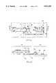
- FIGS. 1a, 1b and 1care schematic diagrams of possible inductance network configurations per the present invention.
- FIGS. 2a-2hare plan views showing a fabrication sequence for integrating inductors and MEM switches per the present invention.
- FIGS. 3a-3hare cross-sectional views which correspond with FIGS. 2a-2h, respectively, showing a fabrication sequence for integrating inductors and MEM switches per the present invention.
- FIGS. 4a and 4bare plan and cross-sectional views, respectively, of an inductance network utilizing a MEM switch which features two contact electrodes.
- FIG. 5is a schematic diagram of an inductance network used as a component of a low noise amplifier (LNA) front end.
- LNAlow noise amplifier
- FIG. 6is a schematic diagram of an inductance network used as a component of an oscillator.
- FIGS. 1a, 1b and 1cillustrate several possible ways in which the present invention can be configured.
- a number X of inductors L a1 , L a2 , . . . , L axare connected together in series.
- Across each inductor L a1 , L a2 , . . . L axis a respective switch S a1 , S a2 , . . . , S ax which, when closed, causes its respective inductor to be bypassed.
- S axform a switching network 10, which in combination with inductors L a1 , L a2 , . . . , L a1 form a tunable inductance network 12.
- One side of inductor L a1serves as the input IN1 to the inductance network, and one side of inductor L ax serves as the network's output OUT1.
- a control device 14is typically employed to control the state of the switches comprising the switching network.
- the inductance networkis operated by configuring the switching network as needed to provide a desired inductance. For example, assume that the inductance for each of inductors L a1 , L a2 , . . . , L ax is equal to a common value L.
- the inductance present between the input IN1 and output OUT1 of inductance network 10is then selectable between a minimum of 1L (i.e., 1 ⁇ L), accomplished by closing all but one of switches S a1 , S a2 , . . . , S ax , to a maximum of XL, obtained by opening all of switches S a1 , S a2 , . . .
- Steps of 2L, 3L, . . . , (X-1) Lare available in between the minimum and maximum by closing and opening switches appropriately. Closing all of the switches bypasses all of the switches, providing an inductance of nearly zero between IN1 and OUT1.
- This configurationoffers good resolution between 1 ⁇ H and 2 ⁇ H, but at the cost of a smaller overall inductance range than would be present if each inductor were equal to 1 ⁇ H, for example.
- the switching network 10enables the inductance network to be "tunable", i.e., to have an inductance value which can be varied.
- the resolution of an inductance value obtainable with conventional trimming techniquesis subject to certain physical limitations.
- the resolution of a tunable inductor per the inventionis practically unlimited, since fine trimming can be done by switching very small inductors into and out of the inductance network.
- inductors used in resonant circuitsoften are deliberately designed with a low value of Q.
- a lower Q valuebroadens the circuit's bandwidth, so that the passband resulting from less-than-perfect values of L will still pass the frequency of interest. Because of the precision with which an inductance value can be provided with the invention, there is no longer a need to compromise the value of Q.
- Switches S a1 , S a2 , . . . , S axare preferably micro-electromechanical (MEM) switches.
- MEMmicro-electromechanical
- a MEM switch as used hereinrefers to a device having at least one movable metal contact which bridges a gapped signal path when made to move from an "open” position to a "closed” position, typically in response to the application of an actuation signal, and which can be implemented on an I.C. substrate using well-known I.C. fabrication techniques. Switches of this type offer insertion losses as low as 0.1 db at high frequencies, thus making them well-suited for use in a tunable inductance network per the present invention. Circuit inefficiencies and negative effects on Q are substantially reduced when the switching network uses a MEM switch, which make the fabrication of a practical high-Q precisely tunable inductance network possible.
- the preferred MEM switchhas at least one top electrode positioned on a cantilever arm which extends over at least one bottom electrode positioned on an I.C. substrate.
- the cantilever armWhen an actuation voltage is applied across the top and bottom electrodes, the cantilever arm is electrostatically drawn toward the substrate and one or more contact electrodes affixed to the substrate side of the cantilever arm bridge one or more gapped signal lines on the substrate surface, creating continuous signal paths.
- MEM switches as discussed hereinare discussed in Yao and Chang, "A Surface Micromachined Miniature Switch for Telecommunications Applications with Signal Frequencies from DC up to 4 GHz," In Tech. Digest (1995), pp. 384-387 and in U.S. Pat. No. 5,578,976 to Yao, which is assigned to the same assignee as the present application.
- An inductance network 12 per the present inventionpreferably includes a control device 14 which causes the switches in the switching network 10 to be actuated as appropriate to achieve a desired inductance value.
- the control device 14, such as a microprocessor, for example,typically acts in response to an external input 16 which is representative of the desired inductance.
- FIG. 1bA schematic diagram of another possible embodiment of the invention is shown in FIG. 1b.
- a number of inductors L b1 , L b2 , . . . , L bxare configured in parallel, with each inductor having a respective switch S b1 , S b2 , . . . , S bx connected in series with it; the switches form a switching network 20 which in combination with the inductors L b1 , L b2 , . . . , L bx form an inductance network 22.
- the network 22has an input IN2 connected to one side of the switching network and each of the inductors is connected together on one side to form the network's output OUT2.
- the inductance value presented between IN2 and OUT2is set by manipulating the state of the switches making up switching network 20. Any single inductor is imposed into the signal path by closing its respective switch; when the switches of more than one inductor are closed, a parallel combination of the selected inductors is formed.
- Each inductor in the networkcan be fabricated to have the same inductance value, or each can have a unique inductance value. For example, a four-inductor configuration in which the inductors have values of L, L/2, L/4 and L/16, respectively, offers a 16:1 range of inductance values if selected singly, and good resolution when combined in parallel.
- parallel inductance network 22would typically be controlled by a control device 24 which sets the network's inductance value by actuating the switches making up the switching network 20 in response to an external input 26.
- FIG. 1cshows an embodiment of the invention in which a number of inductors can be interconnected in a series/parallel combination.
- Inductors L c1 , L c2 , . . . , L cxare arranged to be selectably connected together in series, with each inductor having a respective bypass switch S c1 , S c2 , . . . , S cx across it.
- One end of switch S cxis connected to a number of inductors L d1 , L d2 , . . . , L dx arranged to be connected together in parallel.
- FIG. 1cAlso shown in FIG. 1c are pairs of switches S c1a /S c1b , S c2a /S c2b , . . . , S cxa /S cxb and S d1a /S d1b , S d2a /S d2b , . . . , S dxa /S dxb around respective inductors, with one switch of each pair connected in series with one end of its respective inductor and the second switch of the pair connected in series with the inductor's other end. Each switch of the pair must be closed for its respective inductor to contribute to the inductance network.
- L dxcomprise an inductance network 32.
- One end of switch S c1serves as an input IN3 to the network 32, and switches S d1b , S d2b , . . . , S dxb are each connected together on one side to form the network's output OUT3.
- Manipulating switching network 30so that some of inductors L c1 , L c2 , . . . , L cx and some of inductors L d1 , L d2 , . . . , L dx are selected to contribute to the network forms a series/parallel combination of inductors, which offers more flexibility in obtaining a specific inductance value from the network 32.
- a desired inductance valuecould be obtained by using series inductors L c1 , L c2 , . . . , L cx as a coarse inductance value adjustment, with the parallel inductors L d1 , L d2 , . . . , L dx selected as necessary to provide a fine adjustment.
- a parallel/series combination of inductorscan be similarly implemented by swapping the respective positions of the parallel inductors L d1 , L d2 , . . . , L dx (and their associated switches) and the series inductors L c1 , L c2 , . . . , L cx .
- the pairs of switches around each inductorserve to completely isolate the inductor when it is not selected. When only one end of an inductor is disconnected from the inductance network, the end that is still connected may cause the inductor to contribute unwanted parasitic capacitance to the network. Problems may also arise from electromagnetic radiation generated by an inductor coil which remains connected at one end, particularly with large coils.
- the "dual switching" approach provided by the switch pairsis preferred when the presence of these conditions would cause an unacceptable level of performance degradation in the circuit in which the inductors are used. However, the use of dual switching does require additional I.C. die space, as two to three times as many switches are required.
- the preferred MEM switchesintroduce very low values of resistance into an inductance network built per the present invention, there are practical limitations on the number of inductors which should be interconnected. As the number of switches interconnected in series increases, and/or the number of switches interconnected in parallel decreases, the overall resistance contributed by the switches goes up. Per Equation 1, as R increases, Q decreases. At some value of R, the value of Q becomes so low that the system specifications can no longer be met.
- the power required to operate the switchesmay also impose a limitation on the number of switches which can be accommodated in a system, particularly one that is battery-powered.
- FIGS. 1a, 1b and 1care intended as merely illustrative.
- An inductance network per the present inventioncan be configured as needed for a specific application, with consideration given to factors such as desired inductance range, desired resolution, number of inductance steps available between minimum and maximum inductance values, power dissipation, and desired Q.
- FIGS. 2a-2hplane views
- 3a-3hcorresponding cross-sectional views
- the fabrication sequence shown, which includes only one switch and one inductor,is intended to merely illustrate the process.
- An inductance network per the present inventionincludes a number of switches and inductors, so that the sequence shown is necessarily repeated as needed to create a complete network.
- a first sacrificial material 40such as a layer of thermal setting polyimide
- a second sacrificial layersuch as a layer of pre-imidized polyimide 44 that can be selectively removed from the first sacrificial layer, is then deposited.
- a layer of silicon nitride 46preferably about 1500 ⁇ thick, is then deposited and patterned using photolithography and reactive ion etching (RIE) in CHF 3 and O 2 chemistry. The pattern is transferred to the underlying polyimide layers using O 2 RIE, resulting in the cross-section shown in FIG. 3a.
- a layer of metalis deposited, preferably by electron beam evaporation, which is about equal in thickness to the first sacrificial layer 40.
- the second sacrificial layer 44, the silicon nitride layer 46 and the metal on top of itare then dissolved away in a solution such a methylene chloride, retaining the metal in the original open areas along with the first sacrificial layer 40.
- This first metal layerdefines the bottom electrode 48 of a MEM switch and the traces 49 which carry a voltage to the electrode, and two metal traces 50 and 51 which form the gapped signal line which is bridged when the switch is actuated.
- Traces 50 and 51also include metal interconnection runs 53a and 53b which connect, for example, to other switches and inductors which make up an inductance network.
- an additional sacrificial polyimide layer 54is deposited (FIG. 3c, not shown in FIG. 2c) and patterned to form sloping sidewalls 56 and 58 using O 2 RIE (FIG. 3d, not shown in FIG. 2d), and a selective deposition of a thick insulating material, preferably silicon dioxide, forms support post 60 for the inductor coils (FIGS. 2d and 3d).
- a thick insulating materialpreferably silicon dioxide
- another layer of metalis deposited and patterned to form the switch's contact electrode 62 and the inductor coils 64 (orthogonal portions of the coils not shown in FIG. 3e for clarity).
- the area where the contact electrode 62 will resideis preferably treated in an O 2 RIE plasma to etch a small amount, preferably 2000 ⁇ -5000 ⁇ , into the topmost sacrificial layer 54, so that the electrode is slightly recessed into the layer.
- a cantilever arm 66is formed from a layer, preferably about 2 ⁇ m thick, of PECVD silicon dioxide, patterned and etched with CHF 3 and O 2 RIE.
- a layer of metalpreferably aluminum about 2500 ⁇ thick, is deposited, preferably using electron beam evaporation and lift-off, to form a top electrode 68 for the switch.
- the top electrode 68preferably comes down the sidewall 56 and a metal trace 69 extends from it; a voltage is applied to the top electrode via trace 69 to actuate the switch.
- the sacrificial layersare removed, preferably with an unpatterned O 2 etch using a Branson O 2 barrel etcher, to remove all remaining polyimide layers on the substrate surface, including those under the cantilever arm 66.
- Thisallows the arm 66 to flex downward in response to an actuation voltage applied across the top electrode 68 via trace 69 and the bottom electrode 48 via trace 49, causing contact electrode 62 to bridge the gap between traces 50 and 52.
- Traces 53a and 53bprovide connections to the outer coil and center tap 52 of the inductor, respectively, as well as to the other inductors and switches which make up the inductance network.
- closing the MEM switchcauses the inductor to be short circuited and effectively bypassed.
- a signal applied to trace 53ais passed through the inductor's coils 64 and continues down trace 53b to other components of the inductance network.
- top electrode 62is preferably slightly recessed into sacrificial layer 54. This is to ensure that when the switch is actuated, the contact electrode 62 bridges the traces 50, 51 before the cantilever arm comes into contact with the bottom electrode 48.
- the substrateis not limited to any particular material, and is properly chosen based on other system considerations.
- a glass substrateis inexpensive, allows large inductors to be formed on it, and reduces parasitic capacitance between the inductors and the substrate.
- Silicon or GaAs substratesmay be preferable, however, if the inductance network is being integrated with other components which require the same substrate material.
- wireless communications devicesoften use high-speed active devices which must be fabricated on a semi-insulating GaAs substrate.
- a device which utilized the present inductance networkcould integrate its active devices with the inductance network on a common GaAs substrate.
- the metal which forms the inductor coilsis preferably made as thick as possible, to reduce their resistance and to increase the inductor's Q.
- the switch's contact electrode 62is formed with the same deposition step as the coils and may become too heavy if made too thick, so that a compromise is necessary between coil thickness and contact thickness. The necessity of making this compromise can be avoided if an alternative fabrication sequence is followed in which the inductors are fabricated on the substrate first, without simultaneously building up the switches. When the inductor fabrication is complete, the sequence picks up with the deposition of the polyimide layers 40 and 44 and the silicon nitride layer 46 as shown in FIG. 2a.
- This methodrequires more processing steps to be executed, but allows for a more flexible choice of inductor design parameters. For example, this approach permits the metal of the inductor coils to be thicker than that of the contact electrode, lowering the resistance of the coils and raising the inductor's Q.
- FIGS. 2a-2h and 3a-3hshows the inductor elevated above the substrate by support post 60. This arrangement is preferred because it reduces parasitic capacitance between the inductor coils and the substrate.
- the coilscan be fabricated directly on an insulating substrate, with the center tap brought out over the coils via the use of air bridges.
- MEM switchesbe used which have the capability to bridge two independent gapped signal lines when closed. This capability is attained by including two contact electrodes on the switch's cantilever arm rather than the single contact electrode 62 shown in FIGS. 2e-2h and 3e-3h.
- a double-throw MEM switch with two contact electrodes integrated with an inductoris shown in FIG. 4.
- Two gapped signal lines 70 and 72are positioned on a substrate 73 below a MEM switch 74.
- the switch 74has two contact electrodes 75 and 76, with electrode 75 positioned to bridge gapped signal line 70 when closed, and electrode 76 positioned to bridge gapped signal line 72 when closed.
- Inductor 82is shown fabricated directly on the substrate 73, with connection to the center tap 78 provided by an air bridge 84. When an inductor's coils lie directly on the substrate 73, the substrate must be an insulating substrate to prevent the coils from being shorted together.
- the MEM switch depicted in FIGS. 2, 3 and 4represent only two of many possible configurations of such a switch.
- the cantilever arm and electrodesmay be formed in various geometries and using various materials as appropriate for a given end use.
- the low loss characteristics provided by using one or more movable metal contacts to make electrical connectionsis essential to realizing the benefits of the invention herein claimed.
- the inductance network 12is used as a component of a front end circuit for a low noise amplifier (LNA), which would typically be used to amplify signals received by an antenna 90. Signals received by the antenna are passed through tunable inductance network 12 to the control input of an active device Q1.
- Q1is usually a GaAs FET (shown) or a bipolar junction transistor.
- a fixed inductor L1is connected between Q1's source and ground, and Q1's drain serves as the output of the front end circuit.
- the inductance network 12is preferably controlled by a control device 14, which typically sets the switches in the network in response to an external input 16.
- Fixed inductor L1 and inductance network 12form a resonant circuit that determines the front end's frequency response; the circuit's resonant frequency is dependent on the inductance value of the network 12.
- Having a tunable inductance value in an LNA applicationprovides advantages in at least two ways.
- An LNA in a cordless phonefor example, ideally amplifies incoming signals of one specific frequency only, such as 900 MHz, while blocking all other frequencies.
- Use of an inductor with a high Qproduces a sharp peak at the resonant frequency, but if its L value is slightly off the desired inductance, the LNA may have much less gain at the desired frequency.
- a lower Q inductorSince it is difficult to obtain a conventional inductor having an L value which is sufficiently close to the desired L value, a lower Q inductor must often be employed to ensure that the frequency of interest will be passed.
- Using a tunable inductance networkreduces the need to compromise the value of Q.
- the network 12is simply designed to provide the degree of resolution needed to obtain the specific L value needed by the circuit.
- Each of the fixed inductors which make up the networkcan be high-Q, so that a sharp peak is obtained in the frequency response precisely at the desired frequency.
- An LNA front end as shown in FIG. 5can be fabricated on a common substrate 94 (shown schematically), if desired.
- the inventioncan be implemented on a variety of substrates, including GaAs, glass and silicon types.
- the inductance networkcan thus be integrated with active devices requiring any of these substrate types.
- the tunable inductance networkcan also be used to permit an LNA to be adaptable for use with different communications standards.
- the standard frequency for U.S. cellular phone communicationsis 900 MHz
- the European standardis 1.9 GHz.
- Using a tunable inductance networkenables the LNA to be adapted to either system by simply commanding the network's switching network to interconnect its fixed inductors as needed to provide resonance at one standard or the other.
- To accommodate the 1 GHz range of this examplewould require an inductance value adjustment range of about 4:1, which is well within the capabilities of the present invention.
- the LNA application shown in FIG. 5is not limited to the use of series-connected inductance network 12. Any of the configurations described above, including parallel inductance network 22 and combination series/parallel inductance network 32 are equally acceptable, with the particular configuration determined by system requirements. Similarly, the arrangement of components around Q1 is not limited to that shown in FIG. 5, which is intended only to illustrate the invention's use in an LNA application. For example, an LNA having a frequency response peak which is determined by the L value of network 12 and the inductance of L1 can also be implemented with inductor L1 between the antenna 90 and the gate of Q1 and network 12 in Q1's source circuit.
- an inductance network per the present inventionwould typically be employed: as a high-precision fixed inductor and as a tunable inductor.
- the tunable inductance networkcan serve as a trimmed inductor, but with a higher degree of accuracy than is attainable with conventional trimming techniques.
- the networkis fabricated, its switching network is operated and its inductance measured until the specific value of L is attained.
- the final configuration of network switchesis preserved; for example (as shown in FIG. 5), a memory device 92 associated with control device 14 can store the switch configuration so that the desired L value can be made available upon demand.
- the inductance of the inductance networkis made to vary in the field as needed.
- an external input 16 to the control device 14may indicate that the resonant frequency of the LNA circuit needs to be changed to accommodate a different frequency standard.
- the control devicewould typically be programmed to respond to this input by changing the configuration of switches as necessary to produce the new resonant frequency.
- an oscillatoris formed from an amplifier A1 which has a capacitor C2 and a tunable inductance network 12 with inductance value L in a feedback path; the values of L and C2 determine the oscillator's output frequency f out .
- the need for a very precise oscillator frequencyis common in RF circuits, to provide a local oscillator signal to a down-converter, for example.
- Use of a tunable inductance network 12 as a high-precision fixed inductor as described aboveenables a specific fixed frequency to be generated and maintained.
- the network 12can be used as a tunable inductor and allow different output frequencies to be generated as needed.
- the number of inductors and switches needed to create an inductance network with a wide inductance range and fine resolutionmay be large, and the die area required to accommodate such a network can also be quite large.
- a series inductance network as shown in FIG. 1acomprises 10 inductors and 10 switches, with the 10 inductors having inductance values of 1L, 0.9L, 0.8L, 0.7L, 0.6L, 0.5L, 0.4L, 0.3L, 0.2L and 0.1L, respectively.
- This configurationprovides an inductance range of between 0 and 5.5L, and a resolution of 0.1L.
- the die space occupied by each inductorvaries with its inductance; a typical area is about 250 ⁇ 250 ⁇ .
- the preferred MEM switchoccupies about 1 mm ⁇ 300 ⁇ . Ignoring the necessary spacing between devices on a die, this inductance network would consume about 3.6 ⁇ 10 6 ⁇ 2 . Though the complexity of the inductance network and the very large die area which it requires are burdensome, the burden is more than offset by the unprecedented accuracy and quality factor specifications made possible by the invention, which enable levels of performance in RF communications equipment that have been heretofore unattainable.
Landscapes
- Engineering & Computer Science (AREA)
- Power Engineering (AREA)
- Microelectronics & Electronic Packaging (AREA)
- Semiconductor Integrated Circuits (AREA)
Abstract
Description
Claims (25)
Priority Applications (2)
| Application Number | Priority Date | Filing Date | Title |
|---|---|---|---|
| US08/848,137US5872489A (en) | 1997-04-28 | 1997-04-28 | Integrated tunable inductance network and method |
| US09/086,181US6232847B1 (en) | 1997-04-28 | 1998-05-28 | Trimmable singleband and tunable multiband integrated oscillator using micro-electromechanical system (MEMS) technology |
Applications Claiming Priority (1)
| Application Number | Priority Date | Filing Date | Title |
|---|---|---|---|
| US08/848,137US5872489A (en) | 1997-04-28 | 1997-04-28 | Integrated tunable inductance network and method |
Related Parent Applications (1)
| Application Number | Title | Priority Date | Filing Date |
|---|---|---|---|
| US08/848,116Continuation-In-PartUS5880921A (en) | 1997-04-28 | 1997-04-28 | Monolithically integrated switched capacitor bank using micro electro mechanical system (MEMS) technology |
Related Child Applications (1)
| Application Number | Title | Priority Date | Filing Date |
|---|---|---|---|
| US08/985,564Continuation-In-PartUS5994985A (en) | 1997-04-28 | 1997-12-05 | Integrable high-Q tunable capacitor and method |
Publications (1)
| Publication Number | Publication Date |
|---|---|
| US5872489Atrue US5872489A (en) | 1999-02-16 |
Family
ID=25302446
Family Applications (1)
| Application Number | Title | Priority Date | Filing Date |
|---|---|---|---|
| US08/848,137Expired - LifetimeUS5872489A (en) | 1997-04-28 | 1997-04-28 | Integrated tunable inductance network and method |
Country Status (1)
| Country | Link |
|---|---|
| US (1) | US5872489A (en) |
Cited By (95)
| Publication number | Priority date | Publication date | Assignee | Title |
|---|---|---|---|---|
| US6049702A (en)* | 1997-12-04 | 2000-04-11 | Rockwell Science Center, Llc | Integrated passive transceiver section |
| US6060759A (en)* | 1998-03-06 | 2000-05-09 | International Business Machines Corporation | Method and apparatus for creating improved inductors for use with electronic oscillators |
| DE19925742A1 (en)* | 1999-06-05 | 2000-12-07 | Inst Halbleiterphysik Gmbh | Oscillator application in GHz frequency range, has resonant circuit in which inductance is periodically switched in parallel with further inductance via switching device operated with oscillator frequency |
| WO2001003288A1 (en)* | 1999-07-01 | 2001-01-11 | Rockwell Science Center, Llc | Integrated tunable high efficiency power amplifier |
| US6215644B1 (en) | 1999-09-09 | 2001-04-10 | Jds Uniphase Inc. | High frequency tunable capacitors |
| US6229684B1 (en) | 1999-12-15 | 2001-05-08 | Jds Uniphase Inc. | Variable capacitor and associated fabrication method |
| US6232847B1 (en)* | 1997-04-28 | 2001-05-15 | Rockwell Science Center, Llc | Trimmable singleband and tunable multiband integrated oscillator using micro-electromechanical system (MEMS) technology |
| US6300830B1 (en)* | 2000-12-29 | 2001-10-09 | Ericsson Inc | Multiplexed input envelope restoration scheme for linear high-efficiency power amplification |
| US6310419B1 (en) | 2000-04-05 | 2001-10-30 | Jds Uniphase Inc. | Resistor array devices including switch contacts operated by microelectromechanical actuators and methods for fabricating the same |
| DE10021273A1 (en)* | 1999-06-05 | 2001-10-31 | Inst Halbleiterphysik Gmbh | Variable inductance oscillator |
| WO2002035699A1 (en)* | 2000-10-26 | 2002-05-02 | Siemens Aktiengesellschaft | Voltage-controlled oscillator, especially for mobile radiotelephone devices |
| US6424074B2 (en) | 1999-01-14 | 2002-07-23 | The Regents Of The University Of Michigan | Method and apparatus for upconverting and filtering an information signal utilizing a vibrating micromechanical device |
| WO2002079076A1 (en)* | 2001-03-30 | 2002-10-10 | Jds Uniphase Corporation | Mems device members having portions that contact a substrate and associated mehtods of operating |
| US6472257B2 (en)* | 1997-10-23 | 2002-10-29 | Stmicroelectronics S.R.L. | High quality factor, integrated inductor and production method thereof |
| US6472962B1 (en)* | 2001-05-17 | 2002-10-29 | Institute Of Microelectronics | Inductor-capacitor resonant RF switch |
| DE10163262A1 (en)* | 2001-04-23 | 2002-12-05 | Hans Wolfgang Diesing | Circuit for physiologically optimized digital setting, detection of electrical, electronic values, produces values from optional staged combinations of series and parallel connections |
| US6539253B2 (en) | 2000-08-26 | 2003-03-25 | Medtronic, Inc. | Implantable medical device incorporating integrated circuit notch filters |
| US6549096B2 (en) | 2001-03-19 | 2003-04-15 | International Business Machines Corporation | Switched inductor/varactor tuning circuit having a variable integrated inductor |
| US6567703B1 (en) | 2000-11-08 | 2003-05-20 | Medtronic, Inc. | Implantable medical device incorporating miniaturized circuit module |
| US6566786B2 (en) | 1999-01-14 | 2003-05-20 | The Regents Of The University Of Michigan | Method and apparatus for selecting at least one desired channel utilizing a bank of vibrating micromechanical apparatus |
| US6577040B2 (en) | 1999-01-14 | 2003-06-10 | The Regents Of The University Of Michigan | Method and apparatus for generating a signal having at least one desired output frequency utilizing a bank of vibrating micromechanical devices |
| US20030122246A1 (en)* | 2001-12-31 | 2003-07-03 | Mou-Shiung Lin | Integrated chip package structure using silicon substrate and method of manufacturing the same |
| US6593831B2 (en) | 1999-01-14 | 2003-07-15 | The Regents Of The University Of Michigan | Method and apparatus for filtering signals in a subsystem including a power amplifier utilizing a bank of vibrating micromechanical apparatus |
| US6600252B2 (en) | 1999-01-14 | 2003-07-29 | The Regents Of The University Of Michigan | Method and subsystem for processing signals utilizing a plurality of vibrating micromechanical devices |
| US20030171109A1 (en)* | 2002-03-07 | 2003-09-11 | Motorola, Inc. | Integrated frequency selectable resonant coupling network and method thereof |
| US20030205804A1 (en)* | 2001-12-31 | 2003-11-06 | Jin-Yuan Lee | Integrated chip package structure using ceramic substrate and method of manufacturing the same |
| US20030214015A1 (en)* | 2002-05-17 | 2003-11-20 | Nec Electronics Corporation | Semiconductor device |
| US6713938B2 (en) | 1999-01-14 | 2004-03-30 | The Regents Of The University Of Michigan | Method and apparatus for filtering signals utilizing a vibrating micromechanical resonator |
| US6731492B2 (en) | 2001-09-07 | 2004-05-04 | Mcnc Research And Development Institute | Overdrive structures for flexible electrostatic switch |
| US20040100341A1 (en)* | 2002-11-22 | 2004-05-27 | Luetzelschwab Roland C. | Mems-tuned high power, high efficiency, wide bandwidth power amplifier |
| US20040183606A1 (en)* | 2003-03-04 | 2004-09-23 | Renesas Technology Corp. | Oscillator circuit and L load differential circuit achieving a wide oscillation frequency range and low phase noise characteristics |
| US20040251983A1 (en)* | 2003-06-10 | 2004-12-16 | International Business Machines Corporation | Programmable impedance matching circuit and method |
| US20050068146A1 (en)* | 2003-09-25 | 2005-03-31 | Darryl Jessie | Variable inductor for integrated circuit and printed circuit board |
| US20050090222A1 (en)* | 2003-10-24 | 2005-04-28 | Knecht Thomas A. | Tuneable frequency translator |
| US20050180521A1 (en)* | 2004-02-18 | 2005-08-18 | International Business Machines Corporation | Redundancy structure and method for high-speed serial link |
| US20050231303A1 (en)* | 2004-04-16 | 2005-10-20 | Chao-Liang Chang | Tunable passive device |
| US20050248402A1 (en)* | 2004-05-10 | 2005-11-10 | Li Zhenbiao | Dual-band CMOS front-end with two gain modes |
| US20060033602A1 (en)* | 2004-08-16 | 2006-02-16 | Thomas Mattsson | Variable integrated inductor |
| US20060050350A1 (en)* | 2002-12-10 | 2006-03-09 | Koninklijke Philips Electronics N.V. | Driving of an array of micro-electro-mechanical-system (mems) elements |
| US20060139121A1 (en)* | 2003-02-22 | 2006-06-29 | Jaemyoung Jhung | Fbar band pass filter, duplexer having the filter and methods for manufacturing the same |
| EP1691480A1 (en)* | 2005-02-15 | 2006-08-16 | Samsung Electronics Co., Ltd. | Parallel-structured switched inductor circuit |
| US20060197642A1 (en)* | 2005-03-04 | 2006-09-07 | Michael Hargrove | Variable inductor technique |
| US20070018767A1 (en)* | 2005-07-19 | 2007-01-25 | Lctank Llc | Fabrication of inductors in transformer based tank circuitry |
| US20070018741A1 (en)* | 2005-07-19 | 2007-01-25 | Lctank Llc | Mutual inductance in transformer based tank circuitry |
| US20070072640A1 (en)* | 2005-09-29 | 2007-03-29 | Leininger Kristen M | Electrically adaptive mechanical connection for electronic devices |
| US20070075799A1 (en)* | 2005-10-04 | 2007-04-05 | National Taiwan University Of Science And Technology | Dual-band voltage controlled oscillator utilizing switched feedback technology |
| US7202768B1 (en) | 2003-12-10 | 2007-04-10 | Dsp Group Inc. | Tunable inductor |
| US20070170957A1 (en)* | 2005-07-19 | 2007-07-26 | Lctank Llc | Frequency adjustment techniques in coupled lc tank circuits |
| US7298238B1 (en) | 2006-12-15 | 2007-11-20 | The United States Of America As Represented By The Secretary Of The Navy | Programmable microtransformer |
| US20080007358A1 (en)* | 2005-07-19 | 2008-01-10 | Lctank Llc | RF Stimulus Used to Synchronize a Clock Network |
| DE102006044570A1 (en)* | 2006-09-21 | 2008-04-03 | Atmel Duisburg Gmbh | Integrated circuit arrangement and integrated circuit |
| US20080119363A1 (en)* | 2005-01-17 | 2008-05-22 | Centre National De La Recherche Scientifque | Use of Superconductor Components in Thin Layers as Variable Inductance and Devices Including Said Components and Corresponding Control Method |
| US20080136572A1 (en)* | 2006-12-06 | 2008-06-12 | Farrokh Ayazi | Micro-electromechanical switched tunable inductor |
| US20080305749A1 (en)* | 2007-06-07 | 2008-12-11 | Vishay Intertechnology, Inc | Digitally controlled antenna tuning circuit for radio frequency receivers |
| US20080305750A1 (en)* | 2007-06-07 | 2008-12-11 | Vishay Intertechnology, Inc | Miniature sub-resonant multi-band vhf-uhf antenna |
| US20090085668A1 (en)* | 2007-09-27 | 2009-04-02 | Nanoamp Solutions Inc. (Cayman) | Inductor Sharing in Radio Frequency Communications |
| US20090085671A1 (en)* | 2007-09-27 | 2009-04-02 | Nanoamp Solutions Inc. (Cayman) | Load inductor sharing |
| US20090153284A1 (en)* | 2007-12-17 | 2009-06-18 | Gm Global Technology Operations, Inc. | Inductor packaging for power converters |
| US20090191838A1 (en)* | 2008-01-24 | 2009-07-30 | Samsung Electronics Co., Ltd. | Mode-switching low-noise amplifier and wide-band rf receiver |
| US20090201100A1 (en)* | 2008-02-12 | 2009-08-13 | Kossel Marcel A | Inductor combining primary and secondary coils with phase shifting |
| US20090201101A1 (en)* | 2008-02-12 | 2009-08-13 | Kossel Marcel A | Inductor and method of operating an inductor by combining primary and secondary coils with coupling structures |
| WO2009120587A1 (en)* | 2008-03-26 | 2009-10-01 | International Business Machines Corporation | Inductor having opening enclosed within conductive line and related method |
| US7633356B2 (en) | 2004-02-27 | 2009-12-15 | Centre National De La Recherche Scientifique | Tunable-inductance thin-layered superconductor components, method for the production thereof and devices including said components |
| JP2009302748A (en)* | 2008-06-11 | 2009-12-24 | Toshiba Corp | Amplifier and amplifier module |
| US20090322632A1 (en)* | 2008-06-26 | 2009-12-31 | Ati Technologies Ulc | Physically small tunable narrow band antenna |
| WO2010094784A1 (en)* | 2009-02-19 | 2010-08-26 | Cambridge Silicon Radio Limited | Tuning circuit |
| US7790491B1 (en)* | 2008-05-07 | 2010-09-07 | National Semiconductor Corporation | Method for forming non-volatile memory cells and related apparatus and system |
| US20100295625A1 (en)* | 2009-05-25 | 2010-11-25 | Nec Electronics Corporation | Variable inductor |
| US20110084772A1 (en)* | 2009-10-12 | 2011-04-14 | Cyclos Semiconductor, Inc. | Method for selecting natural frequency in resonant clock distribution networks with no inductor overhead |
| US20110165848A1 (en)* | 2010-01-06 | 2011-07-07 | Oleksandr Gorbachov | Transmit-receive radio frequency front end integrated circuits for laptop computer applications |
| US20110210761A1 (en)* | 2007-05-23 | 2011-09-01 | Ishii Alexander T | Resonant Clock And Interconnect Architecture For Digital Devices With Multiple Clock Networks |
| US20120307229A1 (en)* | 2011-04-29 | 2012-12-06 | Conroy Richard Michael | Resonant modulation for low power range imaging cameras |
| US8399988B2 (en) | 1999-03-01 | 2013-03-19 | Megica Corporation | High performance sub-system design and assembly |
| US8421222B2 (en) | 2002-10-25 | 2013-04-16 | Megica Corporation | Chip package having a chip combined with a substrate via a copper pillar |
| US8426958B2 (en) | 2005-05-03 | 2013-04-23 | Megica Corporation | Stacked chip package with redistribution lines |
| US8471361B2 (en) | 2001-12-31 | 2013-06-25 | Megica Corporation | Integrated chip package structure using organic substrate and method of manufacturing the same |
| US8492870B2 (en) | 2002-01-19 | 2013-07-23 | Megica Corporation | Semiconductor package with interconnect layers |
| US8836443B2 (en)* | 2010-03-26 | 2014-09-16 | Altera Corporation | Integrated circuits with configurable inductors |
| US20140306663A1 (en)* | 2013-04-15 | 2014-10-16 | Virginia Tech Intellectual Properties, Inc. | Energy Storage for Power Factor Correction in Battery Charger for Electric-Powered Vehicles |
| US8963674B2 (en) | 2010-12-20 | 2015-02-24 | Mediatek Singapore Pte. Ltd. | Tunable inductor |
| CN104426564A (en)* | 2013-08-29 | 2015-03-18 | 联芯科技有限公司 | Multi-mode receiver radio frequency front-end system and signal receiving method thereof |
| US20150170816A1 (en)* | 2013-12-18 | 2015-06-18 | Taiwan Semiconductor Manufacturing Company, Ltd. | Varainductor having a spiral inductor, voltage controlled oscillator including the varainductor, and phase locked loop including the varainductor |
| GB2523443A (en)* | 2013-12-11 | 2015-08-26 | Harada Ind Co Ltd | Composite antenna device |
| US9270249B2 (en) | 2012-08-20 | 2016-02-23 | Htc Corporation | Tunable impedance matching circuit |
| US9583250B2 (en) | 2013-09-03 | 2017-02-28 | The United States Of America As Represented By The Secretary Of The Army | MEMS tunable inductor |
| CN106712736A (en)* | 2016-09-29 | 2017-05-24 | 锐迪科微电子(上海)有限公司 | Passive network with adjustable broadband |
| US20170154725A1 (en)* | 2015-11-30 | 2017-06-01 | Intel Corporation | Reconfigurable coupled inductor |
| TWI596893B (en)* | 2013-09-10 | 2017-08-21 | 高效電源轉換公司 | High efficiency voltage mode class d topology |
| US20190074810A1 (en)* | 2016-05-17 | 2019-03-07 | Murata Manufacturing Co., Ltd. | Switch component, high-frequency module, and communication apparatus |
| US20190123735A1 (en)* | 2008-02-28 | 2019-04-25 | Psemi Corporation | Methods and Apparatuses for Use in Tuning Reactance in a Circuit Device |
| US10622992B2 (en) | 2007-04-26 | 2020-04-14 | Psemi Corporation | Tuning capacitance to enhance FET stack voltage withstand |
| CN112615596A (en)* | 2020-12-23 | 2021-04-06 | 陕西烽火电子股份有限公司 | Low-loss tuning matching network |
| US11121587B2 (en)* | 2017-05-19 | 2021-09-14 | Omron Corporation | Non-contact power supply device capable of performing constant voltage output operation |
| CN114280390A (en)* | 2020-09-27 | 2022-04-05 | 湖南金缆电工科技有限责任公司 | A circuit fault troubleshooting device |
| US20230200781A1 (en)* | 2021-01-22 | 2023-06-29 | Exo Imaging, Inc. | Equalization for matrix based line imagers for ultrasound imaging systems |
Citations (9)
| Publication number | Priority date | Publication date | Assignee | Title |
|---|---|---|---|---|
| US2295173A (en)* | 1940-06-20 | 1942-09-08 | Sonora Radio & Television Corp | Step-wise tuning of electrical circuits |
| US2296100A (en)* | 1940-02-20 | 1942-09-15 | Rca Corp | Frequency modulated wave receiver |
| US3087110A (en)* | 1958-07-15 | 1963-04-23 | Tomonoh Haruki | Inductor switching circuit for tv tuner |
| US3427569A (en)* | 1966-12-23 | 1969-02-11 | Ibm | Oscillator apparatus for generating tone frequencies |
| US4564843A (en)* | 1981-06-18 | 1986-01-14 | Cooper Charles E | Antenna with P.I.N. diode switched tuning inductors |
| US4613824A (en)* | 1983-12-16 | 1986-09-23 | Telefunken Electronic Gmbh | Selective amplifier having common base connected transistor and inductive input signal coupling |
| US4701732A (en)* | 1986-12-16 | 1987-10-20 | Hughes Aircraft Company | Fast tuning RF network inductor |
| US5416356A (en)* | 1993-09-03 | 1995-05-16 | Motorola, Inc. | Integrated circuit having passive circuit elements |
| US5578976A (en)* | 1995-06-22 | 1996-11-26 | Rockwell International Corporation | Micro electromechanical RF switch |
- 1997
- 1997-04-28USUS08/848,137patent/US5872489A/ennot_activeExpired - Lifetime
Patent Citations (9)
| Publication number | Priority date | Publication date | Assignee | Title |
|---|---|---|---|---|
| US2296100A (en)* | 1940-02-20 | 1942-09-15 | Rca Corp | Frequency modulated wave receiver |
| US2295173A (en)* | 1940-06-20 | 1942-09-08 | Sonora Radio & Television Corp | Step-wise tuning of electrical circuits |
| US3087110A (en)* | 1958-07-15 | 1963-04-23 | Tomonoh Haruki | Inductor switching circuit for tv tuner |
| US3427569A (en)* | 1966-12-23 | 1969-02-11 | Ibm | Oscillator apparatus for generating tone frequencies |
| US4564843A (en)* | 1981-06-18 | 1986-01-14 | Cooper Charles E | Antenna with P.I.N. diode switched tuning inductors |
| US4613824A (en)* | 1983-12-16 | 1986-09-23 | Telefunken Electronic Gmbh | Selective amplifier having common base connected transistor and inductive input signal coupling |
| US4701732A (en)* | 1986-12-16 | 1987-10-20 | Hughes Aircraft Company | Fast tuning RF network inductor |
| US5416356A (en)* | 1993-09-03 | 1995-05-16 | Motorola, Inc. | Integrated circuit having passive circuit elements |
| US5578976A (en)* | 1995-06-22 | 1996-11-26 | Rockwell International Corporation | Micro electromechanical RF switch |
Non-Patent Citations (8)
| Title |
|---|
| J. Jason Yao, M. Frank Chang, "A Surface Micromachines Miniature Switch For Telecommunications Applications With Signal Frequencies From DC up to 4 GHZ", Tech. Digest, 1995, pp. 384-387. |
| J. Jason Yao, M. Frank Chang, A Surface Micromachines Miniature Switch For Telecommunications Applications With Signal Frequencies From DC up to 4 GHZ , Tech. Digest, 1995, pp. 384 387.* |
| Richard C. Dorf, The Engineering Handbook , CRC Press, 1993, pp. 1011 1013.* |
| Richard C. Dorf, The Engineering Handbook, CRC Press, 1993, pp. 1011-1013. |
| W.T. Wang, Introduction to Semiconductor Technology , John Wiley & Sons, 1990, pp. 422 433.* |
| W.T. Wang, Introduction to Semiconductor Technology, John Wiley & Sons, 1990, pp. 422-433. |
| William H. Hayt, Jr., Jack E. Kemmerly, Engineering Circuit Analysis , McGraw Hill, Inc.. 1971, pp. 396 408.* |
| William H. Hayt, Jr., Jack E. Kemmerly, Engineering Circuit Analysis, McGraw-Hill, Inc.. 1971, pp. 396-408. |
Cited By (200)
| Publication number | Priority date | Publication date | Assignee | Title |
|---|---|---|---|---|
| US6232847B1 (en)* | 1997-04-28 | 2001-05-15 | Rockwell Science Center, Llc | Trimmable singleband and tunable multiband integrated oscillator using micro-electromechanical system (MEMS) technology |
| US6472257B2 (en)* | 1997-10-23 | 2002-10-29 | Stmicroelectronics S.R.L. | High quality factor, integrated inductor and production method thereof |
| US6049702A (en)* | 1997-12-04 | 2000-04-11 | Rockwell Science Center, Llc | Integrated passive transceiver section |
| US6060759A (en)* | 1998-03-06 | 2000-05-09 | International Business Machines Corporation | Method and apparatus for creating improved inductors for use with electronic oscillators |
| US6680660B2 (en) | 1999-01-14 | 2004-01-20 | The Regents Of The University Of Michigan | Method and apparatus for selecting at least one desired channel utilizing a bank of vibrating micromechanical apparatus |
| US6593831B2 (en) | 1999-01-14 | 2003-07-15 | The Regents Of The University Of Michigan | Method and apparatus for filtering signals in a subsystem including a power amplifier utilizing a bank of vibrating micromechanical apparatus |
| US6600252B2 (en) | 1999-01-14 | 2003-07-29 | The Regents Of The University Of Michigan | Method and subsystem for processing signals utilizing a plurality of vibrating micromechanical devices |
| US6917138B2 (en) | 1999-01-14 | 2005-07-12 | The Regents Of The University Of Michigan | Method and subsystem for processing signals utilizing a plurality of vibrating micromechanical devices |
| US6577040B2 (en) | 1999-01-14 | 2003-06-10 | The Regents Of The University Of Michigan | Method and apparatus for generating a signal having at least one desired output frequency utilizing a bank of vibrating micromechanical devices |
| US6566786B2 (en) | 1999-01-14 | 2003-05-20 | The Regents Of The University Of Michigan | Method and apparatus for selecting at least one desired channel utilizing a bank of vibrating micromechanical apparatus |
| US20040095210A1 (en)* | 1999-01-14 | 2004-05-20 | The Regents Of The University Of Michigan | Method and subsystem for processing signals utilizing a plurality of vibrating micromechanical devices |
| US6713938B2 (en) | 1999-01-14 | 2004-03-30 | The Regents Of The University Of Michigan | Method and apparatus for filtering signals utilizing a vibrating micromechanical resonator |
| US6424074B2 (en) | 1999-01-14 | 2002-07-23 | The Regents Of The University Of Michigan | Method and apparatus for upconverting and filtering an information signal utilizing a vibrating micromechanical device |
| US8399988B2 (en) | 1999-03-01 | 2013-03-19 | Megica Corporation | High performance sub-system design and assembly |
| DE19925742A1 (en)* | 1999-06-05 | 2000-12-07 | Inst Halbleiterphysik Gmbh | Oscillator application in GHz frequency range, has resonant circuit in which inductance is periodically switched in parallel with further inductance via switching device operated with oscillator frequency |
| DE10021273A1 (en)* | 1999-06-05 | 2001-10-31 | Inst Halbleiterphysik Gmbh | Variable inductance oscillator |
| US6861913B1 (en) | 1999-06-05 | 2005-03-01 | Ihp Gmbh - Innovations For High Performance Microelectronics | Voltage-controlled oscillator with LC resonant circuit |
| US6232841B1 (en) | 1999-07-01 | 2001-05-15 | Rockwell Science Center, Llc | Integrated tunable high efficiency power amplifier |
| WO2001003288A1 (en)* | 1999-07-01 | 2001-01-11 | Rockwell Science Center, Llc | Integrated tunable high efficiency power amplifier |
| JP2003504906A (en)* | 1999-07-01 | 2003-02-04 | イノベイティブ・テクノロジー・ライセンシング・エルエルシー | Integrated tunable and efficient power amplifier |
| EP1206833A4 (en)* | 1999-07-01 | 2005-03-30 | Rockwell Scient Licensing Llc | Integrated tunable high efficiency power amplifier |
| US6215644B1 (en) | 1999-09-09 | 2001-04-10 | Jds Uniphase Inc. | High frequency tunable capacitors |
| US6229684B1 (en) | 1999-12-15 | 2001-05-08 | Jds Uniphase Inc. | Variable capacitor and associated fabrication method |
| US6496351B2 (en) | 1999-12-15 | 2002-12-17 | Jds Uniphase Inc. | MEMS device members having portions that contact a substrate and associated methods of operating |
| US6310419B1 (en) | 2000-04-05 | 2001-10-30 | Jds Uniphase Inc. | Resistor array devices including switch contacts operated by microelectromechanical actuators and methods for fabricating the same |
| US6539253B2 (en) | 2000-08-26 | 2003-03-25 | Medtronic, Inc. | Implantable medical device incorporating integrated circuit notch filters |
| WO2002035699A1 (en)* | 2000-10-26 | 2002-05-02 | Siemens Aktiengesellschaft | Voltage-controlled oscillator, especially for mobile radiotelephone devices |
| US6567703B1 (en) | 2000-11-08 | 2003-05-20 | Medtronic, Inc. | Implantable medical device incorporating miniaturized circuit module |
| US6889084B2 (en) | 2000-11-08 | 2005-05-03 | Medtronic, Inc. | Implantable medical device incorporating miniaturized circuit module |
| US20040015199A1 (en)* | 2000-11-08 | 2004-01-22 | Medtronic, Inc. | Implantable medical device incorporating miniaturized circuit module |
| US6300830B1 (en)* | 2000-12-29 | 2001-10-09 | Ericsson Inc | Multiplexed input envelope restoration scheme for linear high-efficiency power amplification |
| US6549096B2 (en) | 2001-03-19 | 2003-04-15 | International Business Machines Corporation | Switched inductor/varactor tuning circuit having a variable integrated inductor |
| WO2002079076A1 (en)* | 2001-03-30 | 2002-10-10 | Jds Uniphase Corporation | Mems device members having portions that contact a substrate and associated mehtods of operating |
| DE10163262A1 (en)* | 2001-04-23 | 2002-12-05 | Hans Wolfgang Diesing | Circuit for physiologically optimized digital setting, detection of electrical, electronic values, produces values from optional staged combinations of series and parallel connections |
| DE10163262B4 (en)* | 2001-04-23 | 2006-07-06 | Hans Wolfgang Diesing | Circuit for physiologically optimized digital setting, detection of electrical, electronic values, produces values from optional staged combinations of series and parallel connections |
| US6472962B1 (en)* | 2001-05-17 | 2002-10-29 | Institute Of Microelectronics | Inductor-capacitor resonant RF switch |
| US6731492B2 (en) | 2001-09-07 | 2004-05-04 | Mcnc Research And Development Institute | Overdrive structures for flexible electrostatic switch |
| US8471361B2 (en) | 2001-12-31 | 2013-06-25 | Megica Corporation | Integrated chip package structure using organic substrate and method of manufacturing the same |
| US9136246B2 (en) | 2001-12-31 | 2015-09-15 | Qualcomm Incorporated | Integrated chip package structure using silicon substrate and method of manufacturing the same |
| US9030029B2 (en) | 2001-12-31 | 2015-05-12 | Qualcomm Incorporated | Chip package with die and substrate |
| US8835221B2 (en) | 2001-12-31 | 2014-09-16 | Qualcomm Incorporated | Integrated chip package structure using ceramic substrate and method of manufacturing the same |
| US20030205804A1 (en)* | 2001-12-31 | 2003-11-06 | Jin-Yuan Lee | Integrated chip package structure using ceramic substrate and method of manufacturing the same |
| US8535976B2 (en) | 2001-12-31 | 2013-09-17 | Megica Corporation | Method for fabricating chip package with die and substrate |
| US20030122246A1 (en)* | 2001-12-31 | 2003-07-03 | Mou-Shiung Lin | Integrated chip package structure using silicon substrate and method of manufacturing the same |
| US8492870B2 (en) | 2002-01-19 | 2013-07-23 | Megica Corporation | Semiconductor package with interconnect layers |
| US6889036B2 (en)* | 2002-03-07 | 2005-05-03 | Freescale Semiconductor, Inc. | Integrated frequency selectable resonant coupling network and method thereof |
| US20030171109A1 (en)* | 2002-03-07 | 2003-09-11 | Motorola, Inc. | Integrated frequency selectable resonant coupling network and method thereof |
| US20030214015A1 (en)* | 2002-05-17 | 2003-11-20 | Nec Electronics Corporation | Semiconductor device |
| US8421222B2 (en) | 2002-10-25 | 2013-04-16 | Megica Corporation | Chip package having a chip combined with a substrate via a copper pillar |
| US6992543B2 (en)* | 2002-11-22 | 2006-01-31 | Raytheon Company | Mems-tuned high power, high efficiency, wide bandwidth power amplifier |
| US20040100341A1 (en)* | 2002-11-22 | 2004-05-27 | Luetzelschwab Roland C. | Mems-tuned high power, high efficiency, wide bandwidth power amplifier |
| US20060050350A1 (en)* | 2002-12-10 | 2006-03-09 | Koninklijke Philips Electronics N.V. | Driving of an array of micro-electro-mechanical-system (mems) elements |
| US7579926B2 (en)* | 2003-02-22 | 2009-08-25 | Mems Solutions Inc. | FBAR band pass filter, duplexer having the filter and methods for manufacturing the same |
| CN1751435B (en)* | 2003-02-22 | 2010-06-16 | 麦姆斯解决方案有限公司 | FBAR band pass filter, duplexer having the filter and methods for manufacturing the same |
| US20060139121A1 (en)* | 2003-02-22 | 2006-06-29 | Jaemyoung Jhung | Fbar band pass filter, duplexer having the filter and methods for manufacturing the same |
| US20040183606A1 (en)* | 2003-03-04 | 2004-09-23 | Renesas Technology Corp. | Oscillator circuit and L load differential circuit achieving a wide oscillation frequency range and low phase noise characteristics |
| US20070146089A1 (en)* | 2003-03-04 | 2007-06-28 | Renesas Technology Corp. | Oscillator circuit and L load differential circuit achieving a wide oscillation frequency range and low phase noise characteristics |
| US20060071732A1 (en)* | 2003-03-04 | 2006-04-06 | Renesas Technology Corporation | Oscillator circuit and L load differential circuit achieving a wide oscillation frequency range and low phase noise characteristics |
| US7362194B2 (en) | 2003-03-04 | 2008-04-22 | Renesas Technology Corp. | Oscillator circuit and L load differential circuit achieving a wide oscillation frequency range and low phase noise characteristics |
| US7202754B2 (en) | 2003-03-04 | 2007-04-10 | Renesas Technology Corp. | Oscillator circuit and L load differential circuit achieving a wide oscillation frequency range and low phase noise characteristics |
| US7145413B2 (en) | 2003-06-10 | 2006-12-05 | International Business Machines Corporation | Programmable impedance matching circuit and method |
| US20040251983A1 (en)* | 2003-06-10 | 2004-12-16 | International Business Machines Corporation | Programmable impedance matching circuit and method |
| US20050068146A1 (en)* | 2003-09-25 | 2005-03-31 | Darryl Jessie | Variable inductor for integrated circuit and printed circuit board |
| US7460001B2 (en)* | 2003-09-25 | 2008-12-02 | Qualcomm Incorporated | Variable inductor for integrated circuit and printed circuit board |
| US20050090222A1 (en)* | 2003-10-24 | 2005-04-28 | Knecht Thomas A. | Tuneable frequency translator |
| US7158767B2 (en) | 2003-10-24 | 2007-01-02 | Cts Corporation | Tuneable frequency translator |
| US7202768B1 (en) | 2003-12-10 | 2007-04-10 | Dsp Group Inc. | Tunable inductor |
| US7447273B2 (en) | 2004-02-18 | 2008-11-04 | International Business Machines Corporation | Redundancy structure and method for high-speed serial link |
| US20050180521A1 (en)* | 2004-02-18 | 2005-08-18 | International Business Machines Corporation | Redundancy structure and method for high-speed serial link |
| US7633356B2 (en) | 2004-02-27 | 2009-12-15 | Centre National De La Recherche Scientifique | Tunable-inductance thin-layered superconductor components, method for the production thereof and devices including said components |
| US20050231303A1 (en)* | 2004-04-16 | 2005-10-20 | Chao-Liang Chang | Tunable passive device |
| US7167044B2 (en)* | 2004-05-10 | 2007-01-23 | University Of Florida Research Foundation, Inc. | Dual-band CMOS front-end with two gain modes |
| US20050248402A1 (en)* | 2004-05-10 | 2005-11-10 | Li Zhenbiao | Dual-band CMOS front-end with two gain modes |
| WO2005110044A3 (en)* | 2004-05-10 | 2006-03-02 | Univ Florida | Dual-band cmos front-end with two gain modes |
| US7432794B2 (en)* | 2004-08-16 | 2008-10-07 | Telefonaktiebolaget L M Ericsson (Publ) | Variable integrated inductor |
| US20060033602A1 (en)* | 2004-08-16 | 2006-02-16 | Thomas Mattsson | Variable integrated inductor |
| US20080119363A1 (en)* | 2005-01-17 | 2008-05-22 | Centre National De La Recherche Scientifque | Use of Superconductor Components in Thin Layers as Variable Inductance and Devices Including Said Components and Corresponding Control Method |
| US8126523B2 (en) | 2005-01-17 | 2012-02-28 | Centre National De La Recherche Scientifique | Use of superconductor components in thin layers as variable inductance and devices including said components and corresponding control method |
| EP1691480A1 (en)* | 2005-02-15 | 2006-08-16 | Samsung Electronics Co., Ltd. | Parallel-structured switched inductor circuit |
| US20090102572A1 (en)* | 2005-02-15 | 2009-04-23 | Samsung Electronics Co., Ltd. | Parallel-structured switched variable inductor circuit |
| US20060181363A1 (en)* | 2005-02-15 | 2006-08-17 | Samsung Electronics Co., Ltd. | Parallel-structured switched variable inductor circuit |
| US7893786B2 (en) | 2005-02-15 | 2011-02-22 | Samsung Electronics Co., Ltd. | Parallel-structured switched variable inductor circuit |
| US8102218B2 (en) | 2005-02-15 | 2012-01-24 | Samsung Electronics Co., Ltd. | Parallel-structured switched variable inductor circuit |
| US7598838B2 (en)* | 2005-03-04 | 2009-10-06 | Seiko Epson Corporation | Variable inductor technique |
| US20060197642A1 (en)* | 2005-03-04 | 2006-09-07 | Michael Hargrove | Variable inductor technique |
| US8426958B2 (en) | 2005-05-03 | 2013-04-23 | Megica Corporation | Stacked chip package with redistribution lines |
| US7511588B2 (en) | 2005-07-19 | 2009-03-31 | Lctank Llc | Flux linked LC tank circuits forming distributed clock networks |
| US20070176704A1 (en)* | 2005-07-19 | 2007-08-02 | Lctank Llc | Reduced eddy current loss in lc tank circuits |
| US7501903B2 (en) | 2005-07-19 | 2009-03-10 | Lc Tank Llc | Frequency adjustment techniques in coupled LC tank circuits |
| US7508280B2 (en) | 2005-07-19 | 2009-03-24 | Lc Tank Llc | Frequency adjustment techniques in coupled LC tank circuits |
| US20080007358A1 (en)* | 2005-07-19 | 2008-01-10 | Lctank Llc | RF Stimulus Used to Synchronize a Clock Network |
| US20070170957A1 (en)* | 2005-07-19 | 2007-07-26 | Lctank Llc | Frequency adjustment techniques in coupled lc tank circuits |
| US20070018741A1 (en)* | 2005-07-19 | 2007-01-25 | Lctank Llc | Mutual inductance in transformer based tank circuitry |
| US7786836B2 (en) | 2005-07-19 | 2010-08-31 | Lctank Llc | Fabrication of inductors in transformer based tank circuitry |
| US20070018767A1 (en)* | 2005-07-19 | 2007-01-25 | Lctank Llc | Fabrication of inductors in transformer based tank circuitry |
| US20080074202A1 (en)* | 2005-07-19 | 2008-03-27 | Lctank Llc | Multi-phase Closed Loop LC Tank Circuits |
| US7250826B2 (en)* | 2005-07-19 | 2007-07-31 | Lctank Llc | Mutual inductance in transformer based tank circuitry |
| US7429899B2 (en) | 2005-07-19 | 2008-09-30 | Lctank Llc | Reduced eddy current loss in LC tank circuits |
| US20080150668A1 (en)* | 2005-07-19 | 2008-06-26 | Lctank Llc | Generating Variable Inductances by Altering the Physical Characteristics of Inductors Connected in Parallel |
| US20070072640A1 (en)* | 2005-09-29 | 2007-03-29 | Leininger Kristen M | Electrically adaptive mechanical connection for electronic devices |
| US20070075799A1 (en)* | 2005-10-04 | 2007-04-05 | National Taiwan University Of Science And Technology | Dual-band voltage controlled oscillator utilizing switched feedback technology |
| US7227425B2 (en)* | 2005-10-04 | 2007-06-05 | National Taiwan University Of Science And Technology | Dual-band voltage controlled oscillator utilizing switched feedback technology |
| US20080084255A1 (en)* | 2006-09-21 | 2008-04-10 | Samir El Rai | Integrated circuit arrangement and use of connecting lines |
| DE102006044570A1 (en)* | 2006-09-21 | 2008-04-03 | Atmel Duisburg Gmbh | Integrated circuit arrangement and integrated circuit |
| US20080136572A1 (en)* | 2006-12-06 | 2008-06-12 | Farrokh Ayazi | Micro-electromechanical switched tunable inductor |
| US7847669B2 (en)* | 2006-12-06 | 2010-12-07 | Georgia Tech Research Corporation | Micro-electromechanical switched tunable inductor |
| US7298238B1 (en) | 2006-12-15 | 2007-11-20 | The United States Of America As Represented By The Secretary Of The Navy | Programmable microtransformer |
| US7456722B1 (en) | 2006-12-15 | 2008-11-25 | The United States Of America As Represented By The Secretary Of The Navy | Programmable microtransformer |
| US10951210B2 (en) | 2007-04-26 | 2021-03-16 | Psemi Corporation | Tuning capacitance to enhance FET stack voltage withstand |
| US11888468B2 (en) | 2007-04-26 | 2024-01-30 | Psemi Corporation | Tuning capacitance to enhance FET stack voltage withstand |
| US10622992B2 (en) | 2007-04-26 | 2020-04-14 | Psemi Corporation | Tuning capacitance to enhance FET stack voltage withstand |
| US8461873B2 (en) | 2007-05-23 | 2013-06-11 | Cyclos Semiconductor, Inc. | Resonant clock and interconnect architecture for digital devices with multiple clock networks |
| US20110210761A1 (en)* | 2007-05-23 | 2011-09-01 | Ishii Alexander T | Resonant Clock And Interconnect Architecture For Digital Devices With Multiple Clock Networks |
| US8583065B2 (en)* | 2007-06-07 | 2013-11-12 | Vishay Intertechnology, Inc. | Digitally controlled antenna tuning circuit for radio frequency receivers |
| US20080305750A1 (en)* | 2007-06-07 | 2008-12-11 | Vishay Intertechnology, Inc | Miniature sub-resonant multi-band vhf-uhf antenna |
| US20080305749A1 (en)* | 2007-06-07 | 2008-12-11 | Vishay Intertechnology, Inc | Digitally controlled antenna tuning circuit for radio frequency receivers |
| US8126410B2 (en) | 2007-06-07 | 2012-02-28 | Vishay Intertechnology, Inc. | Miniature sub-resonant multi-band VHF-UHF antenna |
| US7649416B2 (en) | 2007-09-27 | 2010-01-19 | Nanoamp Mobile, Inc. | Load inductor sharing |
| US20090085668A1 (en)* | 2007-09-27 | 2009-04-02 | Nanoamp Solutions Inc. (Cayman) | Inductor Sharing in Radio Frequency Communications |
| US20090085671A1 (en)* | 2007-09-27 | 2009-04-02 | Nanoamp Solutions Inc. (Cayman) | Load inductor sharing |
| US7705682B2 (en) | 2007-09-27 | 2010-04-27 | Nanoamp Mobile, Inc. | Inductor sharing in radio frequency communications |
| US7924134B2 (en)* | 2007-12-17 | 2011-04-12 | GM Global Technology Operations LLC | Inductor packaging for power converters |
| US20090153284A1 (en)* | 2007-12-17 | 2009-06-18 | Gm Global Technology Operations, Inc. | Inductor packaging for power converters |
| US20090191838A1 (en)* | 2008-01-24 | 2009-07-30 | Samsung Electronics Co., Ltd. | Mode-switching low-noise amplifier and wide-band rf receiver |
| US20090201100A1 (en)* | 2008-02-12 | 2009-08-13 | Kossel Marcel A | Inductor combining primary and secondary coils with phase shifting |
| US20090201101A1 (en)* | 2008-02-12 | 2009-08-13 | Kossel Marcel A | Inductor and method of operating an inductor by combining primary and secondary coils with coupling structures |
| US8421573B2 (en)* | 2008-02-12 | 2013-04-16 | International Business Machines Corporation | Inductor combining primary and secondary coils with phase shifting |
| US8018312B2 (en)* | 2008-02-12 | 2011-09-13 | International Business Machines Corporation | Inductor and method of operating an inductor by combining primary and secondary coils with coupling structures |
| US12425016B2 (en) | 2008-02-28 | 2025-09-23 | Psemi Corporation | Methods and apparatuses for use in tuning reactance in a circuit device |
| US11258440B2 (en) | 2008-02-28 | 2022-02-22 | Psemi Corporation | Method and apparatus for use in digitally tuning a capacitor in an integrated circuit device |
| US11671091B2 (en) | 2008-02-28 | 2023-06-06 | Psemi Corporation | Devices and methods for improving voltage handling and/or bi-directionality of stacks of elements when connected between terminals |
| US11606087B2 (en)* | 2008-02-28 | 2023-03-14 | Psemi Corporation | Methods and apparatuses for use in tuning reactance in a circuit device |
| US20190123735A1 (en)* | 2008-02-28 | 2019-04-25 | Psemi Corporation | Methods and Apparatuses for Use in Tuning Reactance in a Circuit Device |
| US12431890B2 (en) | 2008-02-28 | 2025-09-30 | Psemi Corporation | Devices and methods for improving voltage handling and/or bi-directionality of stacks of elements when connected between terminals |
| US10630284B2 (en) | 2008-02-28 | 2020-04-21 | Psemi Corporation | Devices and methods for improving voltage handling and/or bi-directionality of stacks of elements when connected between terminals |
| US11082040B2 (en) | 2008-02-28 | 2021-08-03 | Psemi Corporation | Devices and methods for improving voltage handling and/or bi-directionality of stacks of elements when connected between terminals |
| US9230725B2 (en) | 2008-03-26 | 2016-01-05 | Globalfoundries Inc. | Methods of designing an inductor having opening enclosed within conductive line |
| WO2009120587A1 (en)* | 2008-03-26 | 2009-10-01 | International Business Machines Corporation | Inductor having opening enclosed within conductive line and related method |
| US8193893B2 (en) | 2008-03-26 | 2012-06-05 | International Business Machines Corporation | Inductor having opening enclosed within conductive line and related method |
| US20090243778A1 (en)* | 2008-03-26 | 2009-10-01 | Mete Erturk | Inductor having opening enclosed within conductive line and related method |
| US7790491B1 (en)* | 2008-05-07 | 2010-09-07 | National Semiconductor Corporation | Method for forming non-volatile memory cells and related apparatus and system |
| JP2009302748A (en)* | 2008-06-11 | 2009-12-24 | Toshiba Corp | Amplifier and amplifier module |
| US8909182B2 (en) | 2008-06-26 | 2014-12-09 | Ati Technologies Ulc | Physically small tunable narrow band antenna |
| US8144064B2 (en)* | 2008-06-26 | 2012-03-27 | Ati Technologies Ulc | Physically small tunable narrow band antenna |
| US20090322632A1 (en)* | 2008-06-26 | 2009-12-31 | Ati Technologies Ulc | Physically small tunable narrow band antenna |
| US20120268228A1 (en)* | 2009-02-19 | 2012-10-25 | Cambridge Silicon Radio Limited | Tuning Circuit |
| US9455687B2 (en)* | 2009-02-19 | 2016-09-27 | Qualcomm Technologies International, Ltd. | Tuning circuit |
| WO2010094784A1 (en)* | 2009-02-19 | 2010-08-26 | Cambridge Silicon Radio Limited | Tuning circuit |
| US20100295625A1 (en)* | 2009-05-25 | 2010-11-25 | Nec Electronics Corporation | Variable inductor |
| US8390386B2 (en)* | 2009-05-25 | 2013-03-05 | Renesas Electronics Corporation | Variable inductor |
| US20110084736A1 (en)* | 2009-10-12 | 2011-04-14 | Cyclos Semiconductor, Inc. | Architecture for controlling clock characteristics |
| US8502569B2 (en) | 2009-10-12 | 2013-08-06 | Cyclos Semiconductor, Inc. | Architecture for operating resonant clock network in conventional mode |
| US8659338B2 (en) | 2009-10-12 | 2014-02-25 | Cyclos Semiconductor, Inc. | Resonant clock distribution network architecture with programmable drivers |
| US20110084772A1 (en)* | 2009-10-12 | 2011-04-14 | Cyclos Semiconductor, Inc. | Method for selecting natural frequency in resonant clock distribution networks with no inductor overhead |
| US20110090019A1 (en)* | 2009-10-12 | 2011-04-21 | Cyclos Semiconductor, Inc. | Architecture for frequency-scaled operation in resonant clock distribution networks |
| US20110140753A1 (en)* | 2009-10-12 | 2011-06-16 | Cyclos Semiconductor, Inc. | Resonant clock distribution network architecture with programmable drivers |
| US8593183B2 (en) | 2009-10-12 | 2013-11-26 | Cyclos Semiconductor, Inc. | Architecture for controlling clock characteristics |
| US20110090018A1 (en)* | 2009-10-12 | 2011-04-21 | Cyclos Semiconductor, Inc. | Architecture for adjusting natural frequency in resonant clock distribution networks |
| US20110084775A1 (en)* | 2009-10-12 | 2011-04-14 | Cyclos Semiconductor, Inc. | Resonant clock distribution network architecture for tracking parameter variations in conventional clock distribution networks |
| US8358163B2 (en) | 2009-10-12 | 2013-01-22 | Cyclos Semiconductor, Inc. | Resonant clock distribution network architecture for tracking parameter variations in conventional clock distribution networks |
| US9041451B2 (en) | 2009-10-12 | 2015-05-26 | Cyclos Semiconductor, Inc. | Resonant clock distribution network architecture for tracking parameter variations in conventional clock distribution networks |
| US8339209B2 (en) | 2009-10-12 | 2012-12-25 | Cyclos Semiconductor, Inc. | Method for selecting natural frequency in resonant clock distribution networks with no inductor overhead |
| US20110084774A1 (en)* | 2009-10-12 | 2011-04-14 | Cyclos Semiconductor, Inc. | Architecture for operating resonant clock network in conventional mode |
| US8400192B2 (en) | 2009-10-12 | 2013-03-19 | Cyclos Semiconductor, Inc. | Architecture for frequency-scaled operation in resonant clock distribution networks |
| US20110084773A1 (en)* | 2009-10-12 | 2011-04-14 | Cyclos Semiconductor, Inc. | Architecture for single-stepping in resonant clock distribution networks |
| US8368450B2 (en)* | 2009-10-12 | 2013-02-05 | Cyclos Semiconductor, Inc. | Architecture for adjusting natural frequency in resonant clock distribution networks |
| US8362811B2 (en) | 2009-10-12 | 2013-01-29 | Cyclos Semiconductor, Inc. | Architecture for single-stepping in resonant clock distribution networks |
| US20110165848A1 (en)* | 2010-01-06 | 2011-07-07 | Oleksandr Gorbachov | Transmit-receive radio frequency front end integrated circuits for laptop computer applications |
| US8417286B2 (en)* | 2010-01-06 | 2013-04-09 | Rfaxis, Inc. | Transmit-receive radio frequency front end integrated circuits for laptop computer applications |
| WO2011085125A1 (en)* | 2010-01-06 | 2011-07-14 | Rfaxis, Inc. | Transmit-receive radio frequency front end integrated circuits for laptop computer applications |
| US8836443B2 (en)* | 2010-03-26 | 2014-09-16 | Altera Corporation | Integrated circuits with configurable inductors |
| US8963674B2 (en) | 2010-12-20 | 2015-02-24 | Mediatek Singapore Pte. Ltd. | Tunable inductor |
| US20120307229A1 (en)* | 2011-04-29 | 2012-12-06 | Conroy Richard Michael | Resonant modulation for low power range imaging cameras |
| US9052395B2 (en)* | 2011-04-29 | 2015-06-09 | Waikatolink Limited | Resonant modulation for low power range imaging cameras |
| US9270249B2 (en) | 2012-08-20 | 2016-02-23 | Htc Corporation | Tunable impedance matching circuit |
| US20140306663A1 (en)* | 2013-04-15 | 2014-10-16 | Virginia Tech Intellectual Properties, Inc. | Energy Storage for Power Factor Correction in Battery Charger for Electric-Powered Vehicles |
| US9914362B2 (en)* | 2013-04-15 | 2018-03-13 | Virginia Tech Intellectual Properties, Inc. | Energy storage for power factor correction in battery charger for electric-powered vehicles |
| CN104426564B (en)* | 2013-08-29 | 2017-05-31 | 联芯科技有限公司 | Radio frequency front-end system of multimode receiver and signal receiving method thereof |
| CN104426564A (en)* | 2013-08-29 | 2015-03-18 | 联芯科技有限公司 | Multi-mode receiver radio frequency front-end system and signal receiving method thereof |
| US9583250B2 (en) | 2013-09-03 | 2017-02-28 | The United States Of America As Represented By The Secretary Of The Army | MEMS tunable inductor |
| US10230341B2 (en) | 2013-09-10 | 2019-03-12 | Efficient Power Conversion Corporation | High efficiency voltage mode class D topology |
| TWI596893B (en)* | 2013-09-10 | 2017-08-21 | 高效電源轉換公司 | High efficiency voltage mode class d topology |
| US9887677B2 (en) | 2013-09-10 | 2018-02-06 | Efficient Power Conversion Corporation | High efficiency voltage mode class D topology |
| GB2523443A (en)* | 2013-12-11 | 2015-08-26 | Harada Ind Co Ltd | Composite antenna device |
| GB2523443B (en)* | 2013-12-11 | 2018-08-08 | Harada Ind Co Ltd | Compact multiple frequency band antenna device with tuning coils |
| US9478344B2 (en)* | 2013-12-18 | 2016-10-25 | Taiwan Semiconductor Manufacturing Company, Ltd. | Phase locked loop including a varainductor |
| US20150170816A1 (en)* | 2013-12-18 | 2015-06-18 | Taiwan Semiconductor Manufacturing Company, Ltd. | Varainductor having a spiral inductor, voltage controlled oscillator including the varainductor, and phase locked loop including the varainductor |
| US9812251B2 (en)* | 2013-12-18 | 2017-11-07 | Taiwan Semiconductor Manufacturing Company, Ltd. | Varainductor and operation method thereof based on mutual capacitance |
| US20170154725A1 (en)* | 2015-11-30 | 2017-06-01 | Intel Corporation | Reconfigurable coupled inductor |
| US10910150B2 (en)* | 2015-11-30 | 2021-02-02 | Intel Corporation | Reconfigurable coupled inductor |
| US10855245B2 (en)* | 2016-05-17 | 2020-12-01 | Murata Manufacturing Co., Ltd. | Switch component, high-frequency module, and communication apparatus |
| US20190074810A1 (en)* | 2016-05-17 | 2019-03-07 | Murata Manufacturing Co., Ltd. | Switch component, high-frequency module, and communication apparatus |
| CN106712736A (en)* | 2016-09-29 | 2017-05-24 | 锐迪科微电子(上海)有限公司 | Passive network with adjustable broadband |
| CN106712736B (en)* | 2016-09-29 | 2021-09-07 | 锐迪科微电子(上海)有限公司 | Adjustable passive network of broadband |
| US11121587B2 (en)* | 2017-05-19 | 2021-09-14 | Omron Corporation | Non-contact power supply device capable of performing constant voltage output operation |
| CN114280390A (en)* | 2020-09-27 | 2022-04-05 | 湖南金缆电工科技有限责任公司 | A circuit fault troubleshooting device |
| CN114280390B (en)* | 2020-09-27 | 2024-12-03 | 安徽国润电力有限公司 | Circuit fault detection device |
| CN112615596A (en)* | 2020-12-23 | 2021-04-06 | 陕西烽火电子股份有限公司 | Low-loss tuning matching network |
| CN112615596B (en)* | 2020-12-23 | 2025-08-15 | 陕西烽火电子股份有限公司 | Low-loss tuning matching network |
| US20230200781A1 (en)* | 2021-01-22 | 2023-06-29 | Exo Imaging, Inc. | Equalization for matrix based line imagers for ultrasound imaging systems |
Similar Documents
| Publication | Publication Date | Title |
|---|---|---|
| US5872489A (en) | Integrated tunable inductance network and method | |
| US6232847B1 (en) | Trimmable singleband and tunable multiband integrated oscillator using micro-electromechanical system (MEMS) technology | |
| US6232841B1 (en) | Integrated tunable high efficiency power amplifier | |
| EP1288977B1 (en) | Micro-electromechanical switch fabricated by simultaneous formation of a resistor and bottom electrode | |
| US6049702A (en) | Integrated passive transceiver section | |
| US7894205B2 (en) | Variable device circuit and method for manufacturing the same | |
| US6535722B1 (en) | Television tuner employing micro-electro-mechanically-switched tuning matrix | |
| US6646525B2 (en) | Microelectro-mechanical system actuator device and reconfigurable circuits utilizing same | |
| US6898450B2 (en) | High temperature superconducting tunable filter with an adjustable capacitance gap | |
| US20020171517A1 (en) | Inductor-capacitor resonant rf switch | |
| EP0309163A2 (en) | A monolithic microwave integrated circuit | |
| US20020186098A1 (en) | Continuously tunable MEMs-based phase shifter | |
| US20090296307A1 (en) | Mems based rf components with vertical motion and parallel-plate structure and manufacture thereof using standard cmos technologies | |
| EP1383234B1 (en) | Varactor with extended tuning range | |
| US7541894B2 (en) | Phase-shifting circuit and multibit phase shifter | |
| US9197188B2 (en) | Wide range continuously tunable capacitor bank | |
| US20070108540A1 (en) | Micro-electromechanical switch, method of manufacturing an integrated circuit including at least one such switch, and an integrated circuit | |
| Prophet et al. | Highly-selective electronically-tunable cryogenic filters using monolithic, discretely-switchable MEMS capacitor arrays | |
| US20020047758A1 (en) | Electrical resonator | |
| EP1227534B1 (en) | Small-sized phase shifter and method of manufacture thereof | |
| KR100393774B1 (en) | Manufacturing method for bandpass filter using thin film bulk acoustic resonator | |
| Schicke et al. | Integrated niobium thin film air bridges as variable capacitors for superconducting GHz electronic circuits | |
| JPH06318836A (en) | Band pass filter | |
| Yu et al. | Wide tuning range MEMS band-pass filter with inductance change | |
| Blondy et al. | Tunable interdigital coplanar filters using MEMS capacitors |
Legal Events
| Date | Code | Title | Description |
|---|---|---|---|
| AS | Assignment | Owner name:ROCKWELL SCIENCE CENTER, INC., CALIFORNIA Free format text:ASSIGNMENT OF ASSIGNORS INTEREST;ASSIGNORS:BARTLETT, JAMES L.;CHANG, MAU CHUNG F.;MARCY, HENRY O., V;AND OTHERS;REEL/FRAME:008518/0227;SIGNING DATES FROM 19970416 TO 19970422 | |
| STCF | Information on status: patent grant | Free format text:PATENTED CASE | |
| FEPP | Fee payment procedure | Free format text:PAYOR NUMBER ASSIGNED (ORIGINAL EVENT CODE: ASPN); ENTITY STATUS OF PATENT OWNER: LARGE ENTITY | |
| REMI | Maintenance fee reminder mailed | ||
| FPAY | Fee payment | Year of fee payment:4 | |
| SULP | Surcharge for late payment | ||
| FPAY | Fee payment | Year of fee payment:8 | |
| AS | Assignment | Owner name:ROCKWELL SCIENCE CENTER, LLC, CALIFORNIA Free format text:MERGER;ASSIGNOR:ROCKWELL SCIENCE CENTER, INC.;REEL/FRAME:018148/0721 Effective date:19970827 | |
| AS | Assignment | Owner name:INNOVATIVE TECHNOLOGY LICENSING, LLC, CALIFORNIA Free format text:CHANGE OF NAME;ASSIGNOR:ROCKWELL TECHNOLOGIES, LLC;REEL/FRAME:018160/0240 Effective date:20010628 Owner name:ROCKWELL TECHNOLOGIES, LLC, CALIFORNIA Free format text:ASSIGNMENT OF ASSIGNORS INTEREST;ASSIGNOR:ROCKWELL SCIENCE CENTER, LLC;REEL/FRAME:018160/0122 Effective date:20000330 Owner name:ROCKWELL SCIENTIFIC LICENSING, LLC, CALIFORNIA Free format text:CHANGE OF NAME;ASSIGNOR:INNOVATIVE TECHNOLOGY LICENSING, LLC;REEL/FRAME:018160/0250 Effective date:20030919 | |
| AS | Assignment | Owner name:TELEDYNE LICENSING, LLC, CALIFORNIA Free format text:CHANGE OF NAME;ASSIGNOR:ROCKWELL SCIENTIFIC LICENSING, LLC;REEL/FRAME:018573/0649 Effective date:20060918 | |
| AS | Assignment | Owner name:TELEDYNE SCIENTIFIC & IMAGING, LLC, CALIFORNIA Free format text:ASSIGNMENT OF ASSIGNORS INTEREST;ASSIGNOR:TELEDYNE LICENSING, LLC;REEL/FRAME:019881/0950 Effective date:20070927 | |
| AS | Assignment | Owner name:SKYWORKS SOLUTIONS, INC., MASSACHUSETTS Free format text:ASSIGNMENT OF ASSIGNORS INTEREST;ASSIGNOR:TELEDYNE SCIENTIFIC & IMAGING, LLC;REEL/FRAME:020035/0776 Effective date:20071029 | |
| FEPP | Fee payment procedure | Free format text:PAYER NUMBER DE-ASSIGNED (ORIGINAL EVENT CODE: RMPN); ENTITY STATUS OF PATENT OWNER: LARGE ENTITY Free format text:PAYOR NUMBER ASSIGNED (ORIGINAL EVENT CODE: ASPN); ENTITY STATUS OF PATENT OWNER: LARGE ENTITY | |
| FPAY | Fee payment | Year of fee payment:12 | |
| AS | Assignment | Owner name:TELEDYNE SCIENTIFIC & IMAGING, LLC, CALIFORNIA Free format text:MERGER;ASSIGNOR:TELEDYNE LICENSING, LLC;REEL/FRAME:027836/0235 Effective date:20111221 |