US5869406A - Method for forming insulating layers between polysilicon layers - Google Patents
Method for forming insulating layers between polysilicon layersDownload PDFInfo
- Publication number
- US5869406A US5869406AUS08/534,901US53490195AUS5869406AUS 5869406 AUS5869406 AUS 5869406AUS 53490195 AUS53490195 AUS 53490195AUS 5869406 AUS5869406 AUS 5869406A
- Authority
- US
- United States
- Prior art keywords
- ozone
- dielectric layer
- organic silane
- layer
- less
- Prior art date
- Legal status (The legal status is an assumption and is not a legal conclusion. Google has not performed a legal analysis and makes no representation as to the accuracy of the status listed.)
- Expired - Lifetime
Links
Images


Classifications
- H—ELECTRICITY
- H01—ELECTRIC ELEMENTS
- H01L—SEMICONDUCTOR DEVICES NOT COVERED BY CLASS H10
- H01L21/00—Processes or apparatus adapted for the manufacture or treatment of semiconductor or solid state devices or of parts thereof
- H01L21/02—Manufacture or treatment of semiconductor devices or of parts thereof
- H01L21/02104—Forming layers
- H01L21/02107—Forming insulating materials on a substrate
- H01L21/02109—Forming insulating materials on a substrate characterised by the type of layer, e.g. type of material, porous/non-porous, pre-cursors, mixtures or laminates
- H01L21/02112—Forming insulating materials on a substrate characterised by the type of layer, e.g. type of material, porous/non-porous, pre-cursors, mixtures or laminates characterised by the material of the layer
- H01L21/02123—Forming insulating materials on a substrate characterised by the type of layer, e.g. type of material, porous/non-porous, pre-cursors, mixtures or laminates characterised by the material of the layer the material containing silicon
- H01L21/02126—Forming insulating materials on a substrate characterised by the type of layer, e.g. type of material, porous/non-porous, pre-cursors, mixtures or laminates characterised by the material of the layer the material containing silicon the material containing Si, O, and at least one of H, N, C, F, or other non-metal elements, e.g. SiOC, SiOC:H or SiONC
- H—ELECTRICITY
- H01—ELECTRIC ELEMENTS
- H01L—SEMICONDUCTOR DEVICES NOT COVERED BY CLASS H10
- H01L21/00—Processes or apparatus adapted for the manufacture or treatment of semiconductor or solid state devices or of parts thereof
- H01L21/02—Manufacture or treatment of semiconductor devices or of parts thereof
- H01L21/02104—Forming layers
- H01L21/02107—Forming insulating materials on a substrate
- H01L21/02109—Forming insulating materials on a substrate characterised by the type of layer, e.g. type of material, porous/non-porous, pre-cursors, mixtures or laminates
- H01L21/02205—Forming insulating materials on a substrate characterised by the type of layer, e.g. type of material, porous/non-porous, pre-cursors, mixtures or laminates the layer being characterised by the precursor material for deposition
- H01L21/02208—Forming insulating materials on a substrate characterised by the type of layer, e.g. type of material, porous/non-porous, pre-cursors, mixtures or laminates the layer being characterised by the precursor material for deposition the precursor containing a compound comprising Si
- H01L21/02211—Forming insulating materials on a substrate characterised by the type of layer, e.g. type of material, porous/non-porous, pre-cursors, mixtures or laminates the layer being characterised by the precursor material for deposition the precursor containing a compound comprising Si the compound being a silane, e.g. disilane, methylsilane or chlorosilane
- H—ELECTRICITY
- H01—ELECTRIC ELEMENTS
- H01L—SEMICONDUCTOR DEVICES NOT COVERED BY CLASS H10
- H01L21/00—Processes or apparatus adapted for the manufacture or treatment of semiconductor or solid state devices or of parts thereof
- H01L21/70—Manufacture or treatment of devices consisting of a plurality of solid state components formed in or on a common substrate or of parts thereof; Manufacture of integrated circuit devices or of parts thereof
- H01L21/71—Manufacture of specific parts of devices defined in group H01L21/70
- H01L21/768—Applying interconnections to be used for carrying current between separate components within a device comprising conductors and dielectrics
- H01L21/76801—Applying interconnections to be used for carrying current between separate components within a device comprising conductors and dielectrics characterised by the formation and the after-treatment of the dielectrics, e.g. smoothing
- H01L21/76822—Modification of the material of dielectric layers, e.g. grading, after-treatment to improve the stability of the layers, to increase their density etc.
- H01L21/76828—Modification of the material of dielectric layers, e.g. grading, after-treatment to improve the stability of the layers, to increase their density etc. thermal treatment
- H—ELECTRICITY
- H10—SEMICONDUCTOR DEVICES; ELECTRIC SOLID-STATE DEVICES NOT OTHERWISE PROVIDED FOR
- H10B—ELECTRONIC MEMORY DEVICES
- H10B12/00—Dynamic random access memory [DRAM] devices
- H10B12/01—Manufacture or treatment
- H10B12/02—Manufacture or treatment for one transistor one-capacitor [1T-1C] memory cells
- H10B12/03—Making the capacitor or connections thereto
- H—ELECTRICITY
- H01—ELECTRIC ELEMENTS
- H01L—SEMICONDUCTOR DEVICES NOT COVERED BY CLASS H10
- H01L21/00—Processes or apparatus adapted for the manufacture or treatment of semiconductor or solid state devices or of parts thereof
- H01L21/02—Manufacture or treatment of semiconductor devices or of parts thereof
- H01L21/02104—Forming layers
- H01L21/02107—Forming insulating materials on a substrate
- H01L21/02109—Forming insulating materials on a substrate characterised by the type of layer, e.g. type of material, porous/non-porous, pre-cursors, mixtures or laminates
- H01L21/02112—Forming insulating materials on a substrate characterised by the type of layer, e.g. type of material, porous/non-porous, pre-cursors, mixtures or laminates characterised by the material of the layer
- H01L21/02123—Forming insulating materials on a substrate characterised by the type of layer, e.g. type of material, porous/non-porous, pre-cursors, mixtures or laminates characterised by the material of the layer the material containing silicon
- H01L21/02164—Forming insulating materials on a substrate characterised by the type of layer, e.g. type of material, porous/non-porous, pre-cursors, mixtures or laminates characterised by the material of the layer the material containing silicon the material being a silicon oxide, e.g. SiO2
- H—ELECTRICITY
- H01—ELECTRIC ELEMENTS
- H01L—SEMICONDUCTOR DEVICES NOT COVERED BY CLASS H10
- H01L21/00—Processes or apparatus adapted for the manufacture or treatment of semiconductor or solid state devices or of parts thereof
- H01L21/02—Manufacture or treatment of semiconductor devices or of parts thereof
- H01L21/02104—Forming layers
- H01L21/02107—Forming insulating materials on a substrate
- H01L21/02225—Forming insulating materials on a substrate characterised by the process for the formation of the insulating layer
- H01L21/0226—Forming insulating materials on a substrate characterised by the process for the formation of the insulating layer formation by a deposition process
- H01L21/02263—Forming insulating materials on a substrate characterised by the process for the formation of the insulating layer formation by a deposition process deposition from the gas or vapour phase
- H01L21/02271—Forming insulating materials on a substrate characterised by the process for the formation of the insulating layer formation by a deposition process deposition from the gas or vapour phase deposition by decomposition or reaction of gaseous or vapour phase compounds, i.e. chemical vapour deposition
- Y—GENERAL TAGGING OF NEW TECHNOLOGICAL DEVELOPMENTS; GENERAL TAGGING OF CROSS-SECTIONAL TECHNOLOGIES SPANNING OVER SEVERAL SECTIONS OF THE IPC; TECHNICAL SUBJECTS COVERED BY FORMER USPC CROSS-REFERENCE ART COLLECTIONS [XRACs] AND DIGESTS
- Y10—TECHNICAL SUBJECTS COVERED BY FORMER USPC
- Y10S—TECHNICAL SUBJECTS COVERED BY FORMER USPC CROSS-REFERENCE ART COLLECTIONS [XRACs] AND DIGESTS
- Y10S438/00—Semiconductor device manufacturing: process
- Y10S438/909—Controlled atmosphere
Definitions
- the present inventionrelates to semiconductor integrated circuits and their manufacture. More particularly, the invention relates to a technique for forming an insulating layer between a lower conductive layer and an upper conductive layer in a dynamic random access memory (DRAM) device. But it will be recognized that the invention has a wider range of applicability. Merely by way of example, the invention may be applied in the manufacture of other semiconductor devices and conductive layers made of materials such as polysilicon, aluminum, titanium, tungsten, silicide, and others.
- DRAMdynamic random access memory
- Fabrication stepsgenerally include applying a first polysilicon layer (poly-1), depositing an insulating layer using low pressure chemical vapor deposition (LPCVD) overlying the first polysilicon layer, and then applying a second polysilicon layer (poly-2) overlying the insulating layer.
- poly-1first polysilicon layer
- LPCVDlow pressure chemical vapor deposition
- insulating layer thicknessis still difficult to control, especially for devices have smaller line widths such as those with sub-micron features.
- an insulating layer that is too thickoften causes alignment and etching problems in subsequent steps.
- an insulating layer that is too thinoften creates isolation problems (e.g., short circuit) between the first and the second polysilicon layers.
- insulating layer limitationscan include a high water-absorbability, a high etching rate, and a high shrinkage rate. These limitations often occur by way of insulating layers fabricated using an LPCVD technique. High water-absorbability promotes uncontrollable etching, that is, etching that produces a non-uniform layer. High shrinkage rate causes undesired stress on surfaces of the device which affects device performance and reliability.
- a further limitation with the conventional insulating layer deposited by LPCVDis stringers in certain areas of the cell structure, which is due predominantly to the fully conformal characteristic of the LPCVD film. That is, the fully conformal film creates an upper surface profile characterized by gaps and voids thereon. The stringers are formed in these gaps and voids.
- a method and resulting semiconductor device structure for an inter-layer dielectricis provided.
- the present methodprovides a relatively even and easy to fabricate inter-layer dielectric in a DRAM structure.
- the present inventionprovides a method of fabricating an integrated circuit device.
- the methodincludes providing a partially completed semiconductor device.
- the partially completed semiconductor devicehas a first polysilicon layer thereon.
- the methodalso includes depositing a dielectric layer overlying the polysilicon layer and portions of the partially completed semiconductor device at a pressure of about 1 atmosphere.
- a step of forming a second polysilicon layer overlying portions of the dielectric layeris also included.
- the dielectric layer depositing stepcombines an organic silane and an ozone where the ozone at a relatively low concentration.
- the present inventionprovides a method of forming a dielectric layer.
- the methodincludes combining an organic silane and an ozone at a pressure of about 1 atm.
- the ozoneis at a relatively low concentration.
- the methodalso includes forming an insulating layer from the ozone and the organic silane mixture.
- a further alternative specific embodimentincludes a method of forming an integrated circuit device.
- the methodincludes providing a partially completed device comprising a plurality of regions, where the plurality of regions comprises a first polysilicon region and a field isolation oxide region.
- the methodalso includes introducing a mixture, including an organic silane and an ozone at a pressure of about 1 atmosphere, where the ozone at a relatively low pressure.
- the methodfurther includes forming a dielectric layer from the mixture overlying the plurality of regions.
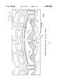
- FIG. 1is a simplified cross-sectional view of conventional DRAM device interconnect layers
- FIG. 2is a detailed cross-sectional view of the stringer in the conventional DRAM device of FIG. 1;
- FIG. 3is a simplified apparatus according to the present invention.
- FIGS. 4-6illustrate a simplified fabrication method according to the present invention.
- FIG. 1is a cross-sectional view of a conventional DRAM device 10.
- the conventional DRAM deviceincludes a first polysilicon layer 12 (or gate electrode layer), an inter-layer dielectric 14 (an insulating layer), and a second polysilicon layer 16, often termed as a bottom capacitor plate.
- the convention DRAM deviceuses a low pressure chemical vapor deposition (LPCVD) technique such as a low pressure tetra ethoxy silane (LP-TEOS) or a low pressure silane (LP-silane) process to deposit the inter-layer dielectric layer 14.
- LPCVDlow pressure chemical vapor deposition
- LP-TEOSlow pressure tetra ethoxy silane
- LP-silanelow pressure silane
- the convention DRAM devicehas an extremely complicated topography 17, which is difficult to cover adequately with the conventional inter-layer dielectric.
- a stringer 18can form in an insulating layer 14 between the first polysilicon layer 12 and the second polysilicon layer 16.
- the stringermay also be at other locations, especially for different types of devices.
- the stringer 18(a portion of the second polysilicon layer) forms and remains in a recessed region (or gas gap) in the insulating layer 14.
- Vapor 22such as H 2 O or O 2 gas is often trapped in the recessed region after deposition of the second polysilicon layer 16.
- the vaporexpands and presses towards the second polysilicon layer.
- the vaporcauses pressure against the second polysilicon layer. This tends to cause failure of the second polysilicon layer, thereby affecting its reliability.
- the vaporpresses towards the capacitor structure 24.
- FIG. 2illustrates a simplified cross-sectional view of a stringer 18 in the DRAM device of FIG. 1.
- the stringeris made of polysilicon or a portion of the second polysilicon layer, which remains in a recessed region (or gap) in the insulating layer.
- the second polysilicon layer portionremains in the recessed region of the insulating layer 14 because the subsequent etching step cannot remove the polysilicon layer portion 18 from its surface, as shown by the thick dashed line.
- the vapor 22is also shown in subsequent heat treatment steps, the vapor expands and presses towards the second polysilicon layer.
- the conventional low pressure chemical vapor deposition methodrelies upon a conventional chemical vapor deposition apparatus.
- the conventional chemical vapor deposition apparatusoften uses deposition pressures of less than 500 millitorr.
- the low deposition pressurerequires sophisticated pumps and chambers, which are often costly and difficult to maintain.
- FIG. 3is a simplified deposition apparatus 300 according to the present invention.
- the apparatus illustratedis merely an example, and should not be construed as limiting the scope of the claims herein.
- the apparatus 300includes a reactor chamber 302, a heater 304, a dispersion head 308, and other elements.
- a semiconductor wafer 306is defined in the reactor chamber 302.
- the heater 304is attached to the lower platen unit of the reactor 302 to control the temperature of the semiconductor wafer.
- the dispersion head 308provides a gas mixture that uniformly contacts the semiconductor wafer 302. Openings 305 to the atmosphere can provide an internal operating pressure in the reaction chamber 302 of about atmospheric pressure, e.g., 1 atm.
- the gas mixtureincludes reactants such as oxygen, ozone, organic silane (e.g., TEOS, HMDS, OMCTS, and others), nitrogen, and other gases.
- the ozoneis generated by an ozone-generator 310 via oxygen introduced into an inlet 316.
- TEOSfor example, liquid TEOS is introduced into a thermostat 312 for vaporization.
- the vaporized TEOSwill be introduced into the dispersion head 308 via line 317.
- An inert gassuch as nitrogen gas is introduced into the dispersion head 308 from inlet 318.
- the inert gasmay behave as a carrier or the like.
- the present methodcan be briefly outlined as follows.
- the ozone gasis introduced into the chamber at a concentration of 100 g/m 3 or less with the organic silane.
- the stepoccurs at a pressure of about 1 atmosphere.
- the combination of the ozone gas and the organic silaneforms a conformal-like, but not fully conformal, dielectric layer.
- the conformal-like dielectric layeris defined by an upper surface substantially free from gaps or voids. This dielectric layer tends to prevent the formation of stringers. Details of the present method are described by way of the following Figs. The method illustrated is merely an example, and should not be construed as limiting the scope of the claims herein.
- the present methodbegins by providing a semiconductor 400 substrate, as illustrated by FIG. 4.
- the semiconductor substratecan be an N-type substrate, a P-type substrate, or any other type of substrate.
- the substratealso includes partially completed device structures 403 and the like.
- the partially completed device structuresare DRAM device structures.
- a patterned metal layer 401is defined overlying a top surface 402 of the substrate.
- the patterned metal layer 401can be a polysilicon layer, an aluminum layer, a titanium tungsten layer, or any other type of metal material, and its combinations.
- the metal layeris often formed by steps of deposition, photolithography, and etching to define an interconnect structure.
- the patterned metal layeris a polysilicon gate layer.
- the polysilicon gate layermay be formed by any suitable technique such as CVD and the like.
- the polysilicon layeris doped with impurities.
- impuritiescan be either P-type or N-type.
- P-type impuritiesinclude boron and others.
- N-type impuritiesinclude arsenic, phosphorous, and the like. Impurities increase the conductivity or reduce the resistivity of the polysilicon layer.
- the polysilicon layermay also be coated with another metal layer such as a silicide or the like. This also reduces resistivity of course, other impurities or metal combinations also can be used depending upon the particular application.
- Sidewall spacers 412are defined on edges of the polysilicon layer 401. Fabrication steps of at least depositing a dielectric layer overlying the polysilicon layer 401, performing an anisotropic etching step on the dielectric layer, and densifying the dielectric layer defines the sidewall spacers.
- the anisotropic etching stepuses a plasma or reactive ion etching technique. During the etching step, horizontal portions of the dielectric layer are removed, leaving the sidewall spacers intact.
- the sidewall spacerscan be made of materials such as silicon nitride, silicon dioxide, combinations thereof, and the like.
- the present methodincludes a step of placing the substrate into a reactor chamber for deposition of an inter-dielectric layer 405.
- the inter-dielectric layeris preferably formed by way of deposition of an organic silane-ozone layer and the like.
- the organic silane-ozone layeris formed by a mixture of ozone gas and an organic silane. A selected combination of ozone gas and organic silane forms a conformal-like, but not fully conformal, dielectric layer, as illustrated by FIG. 5.
- the mixture of organic silane and ozoneis selective adjusted according to the present invention.
- the organic silanecan be tetra ethyl oxy silane (TEOS), hexa methyl disilane (HMDS), octa methyl cyclo tetrasiloxane (OMCTS), and the like.
- Ozoneincludes a concentration of 200 g/m 3 and less, or preferably 150 g/m 3 and less, or more preferably 100 g/m 3 and less, or even more preferably 75 g/m 3 and less.
- a relative flow rate between the ozone and the organic silane such as TEOSranges from about 2.0:4.0 to about 10.0:1.0, and is preferably about 7.5:2.0.
- a deposition temperaturecan be about 300° C. to about 500° C., and is preferably at about 398° C.
- the present dielectric layer before annealingincludes a shrinkage rate of about 10% to about 3%, and is preferably at about 7%. (Note: shrinkage rate ⁇ 1/density)
- the dielectric layeralso is relatively even, that is, the dielectric layer has a uniformity of about 1% to about 3%, and is preferably about 2% or less.
- An etching rate of about 350 ⁇ /min to about 680 ⁇ /min, and preferably at about 540 ⁇ /minare further included.
- the substrateis removed and annealed.
- the annealing processdensities the dielectric layer to seal the underlying integrated circuit elements. This provides a lower and even etch rate for the dielectric layer material. Densification occurs at a temperature of no less than about 800° C., and is preferably at 850° C. and greater. The temperature of the densification does not substantially affect temperature sensitive semiconductor device elements such as a transistor and others.
- the densified dielectric layerhas characteristics that prevent moisture accumulation, and provides for more uniform etching.
- the densified dielectric layerincludes a shrinkage rate of about 0% .
- the densified dielectric layeralso includes a moisture content of about 0%.
- the densified dielectric layeris also relatively even, that is, the densified dielectric layer has a uniformity of 2% to 10%, and is preferably 5% or less.
- the selected characteristics of the densified dielectric layerwill depend upon the particular application. As shown, the densified dielectric layer is substantially even and does not have a site such as a gap or a recessed region for stringer formation.
- the densified dielectric layer, an organic silane-ozone layer, 406 deposited by APCVDis grown overlying the substrate 400, the polysilicon layer 401, and the sidewalls 412, as illustrated by FIG. 6.
- This organic silane-ozone dielectric layer 406 after annealingis a high quality oxide, which also seals underlying integrated circuit elements.
- High quality organic silane-ozone dielectric layer after annealingrefers to a substantially pinhole free layer with consistent density.
- the organic silane-ozone dielectric layeris 1400 ⁇ to about 1800 ⁇ thick, and is preferably 1600 ⁇ thick.
- This dielectric layeris patterned using an etching process. Examples of such an etching process includes plasma etching, reactive ion etching, and others.
- the etching processalso provides a relatively smooth surface 410 without gaps between two portions of the polysilicon layer.
- This smooth surfacehas been created since the dielectric layer was formed with a relatively even topography and provided an even etch rate.
- a wet etch or dip using hydrofluoric acidmay be used to remove any dielectric material such as native oxide before the next process step.
- a second polysilicon layer 407is formed and patterned overlying the dielectric layer.
- An etching stepremoving a portion of the second polysilicon layer does not leave a portion of it in the insulating layer, characteristic of the conventional dielectric layer. Remaining processing steps are performed overlying the second polysilicon layer and portions of the dielectric layer.
- a partially completed waferwas placed into a deposition reactor according to the present invention.
- the partially completed waferwas heated from its backside using a heater element.
- the waferhad a relatively constant temperature of about 398° C.
- ozone and TEOSwere introduced into the reactor chamber.
- the ozone concentrationwas held in the reactor at about 25 ⁇ 5 grams/meter 3 for about 70 to 75 seconds. This provided an insulating layer of about 1600 ⁇ overlying the partially completed wafer.
- the partially completed wafer with the insulating layerunderwent annealing at a temperature of about 850° C. for about 30 minutes.
- the present inventionhad substantial advantages over the conventional techniques.
- the insulating layerwas deposited using a low concentration ozone.
- the low concentration of ozonehad a deposition rate that was not substantially sensitive to the type of material underlying the insulating layer. Accordingly, the insulating layer was substantially consistent, even though portions of it was applied over different types of materials. This makes the present invention compatible with complicated topography using different types of materials, which was often harmful to later etching processes or the like.
- the inventionalso prevented short circuits between the first and second polysilicon layers.
- the inventionprevented leakage current from passing between the first and the second polysilicon layers.
- the insulating layerdid not have undesired features such as a high water-absorbability, a high etching rate, a high shrinkage rate, and other disadvantages.
- the annealing stepdensified the insulating layer and removed water contained therein. This reduces a subsequent etching rate as shown in Table 1.
- the etching rate of present insulating layer with annealingis relative low, as compared to the conventional insulation layer without an anneal.
- the lower etching ratepreserved the present insulation layer during several wet etching steps (e.g., HF etching) to keep the first polysilicon layer isolated from the second polysilicon layer.
- the present inventionfurther provides higher device yields, especially for devices having design rules of 0.5 microns and less.
- the conventional LPCVD deposition of the conventional insulating layeris often very or fully conformal, thereby generating the stringer which occurs after formation of the second polysilicon layer.
- the stringeris harmful for the conventional capacitor structure and results in lower device yields.
- the inventionuses APCVD with low ozone concentrations to deposit the insulation layer which is conformal-like, but not fully conformal, and thus substantially eliminates recessed regions forming under the stringer.
- the insulation layerBy way of the present insulation layer, device yields on a semiconductor wafer are often higher, thereby decreasing the average cost of an integrated circuit and the like.
Landscapes
- Engineering & Computer Science (AREA)
- Manufacturing & Machinery (AREA)
- Physics & Mathematics (AREA)
- Condensed Matter Physics & Semiconductors (AREA)
- General Physics & Mathematics (AREA)
- Computer Hardware Design (AREA)
- Microelectronics & Electronic Packaging (AREA)
- Power Engineering (AREA)
- Internal Circuitry In Semiconductor Integrated Circuit Devices (AREA)
- Semiconductor Memories (AREA)
Abstract
Description
TABLE 1______________________________________Deposition with Ozone Concentration of 25 g/m.sup.3.SAMPLES ETCHING RATE (Å/Min)______________________________________SAMPLE WITH ANNEAL 204SAMPLE WITHOUT ANNEAL 668______________________________________
Claims (25)
Priority Applications (2)
| Application Number | Priority Date | Filing Date | Title |
|---|---|---|---|
| US08/534,901US5869406A (en) | 1995-09-28 | 1995-09-28 | Method for forming insulating layers between polysilicon layers |
| NL1001409ANL1001409C2 (en) | 1995-09-28 | 1995-10-12 | Method for forming insulating layers between polysilicon layers. |
Applications Claiming Priority (3)
| Application Number | Priority Date | Filing Date | Title |
|---|---|---|---|
| US08/534,901US5869406A (en) | 1995-09-28 | 1995-09-28 | Method for forming insulating layers between polysilicon layers |
| NL1001409ANL1001409C2 (en) | 1995-09-28 | 1995-10-12 | Method for forming insulating layers between polysilicon layers. |
| DE19540235ADE19540235C2 (en) | 1995-09-07 | 1995-10-19 | Process for the production of insulating layers in semiconductor devices |
Publications (1)
| Publication Number | Publication Date |
|---|---|
| US5869406Atrue US5869406A (en) | 1999-02-09 |
Family
ID=27215605
Family Applications (1)
| Application Number | Title | Priority Date | Filing Date |
|---|---|---|---|
| US08/534,901Expired - LifetimeUS5869406A (en) | 1995-09-28 | 1995-09-28 | Method for forming insulating layers between polysilicon layers |
Country Status (2)
| Country | Link |
|---|---|
| US (1) | US5869406A (en) |
| NL (1) | NL1001409C2 (en) |
Cited By (7)
| Publication number | Priority date | Publication date | Assignee | Title |
|---|---|---|---|---|
| US6124626A (en)* | 1997-08-22 | 2000-09-26 | Micron Technology, Inc. | Capacitor structures formed using excess oxygen containing material provided relative to electrodes thereof |
| US6509625B1 (en)* | 1998-04-03 | 2003-01-21 | Zetex Plc | Guard structure for bipolar semiconductor device |
| US20050124089A1 (en)* | 2003-12-08 | 2005-06-09 | Gogoi Bishnu P. | Method of forming a seal for a semiconductor device |
| WO2006029651A1 (en)* | 2004-09-16 | 2006-03-23 | S.O.I.Tec Silicon On Insulator Technologies | Method of manufacturing a silicon dioxide layer |
| US20060220082A1 (en)* | 2005-03-17 | 2006-10-05 | Fujitsu Limited | Semiconductor device and manufacturing method of the same |
| KR100845736B1 (en)* | 2007-02-22 | 2008-07-11 | 에스. 오. 이. 떼끄 씰리꽁 오 냉쉴라또흐 떼끄놀로지 | Method for producing silicon dioxide layer |
| WO2008135952A1 (en) | 2007-05-08 | 2008-11-13 | Koninklijke Philips Electronics, N.V. | Active discharge of electrode |
Citations (19)
| Publication number | Priority date | Publication date | Assignee | Title |
|---|---|---|---|---|
| US3614548A (en)* | 1969-06-18 | 1971-10-19 | Matsushita Electronics Corp | Semiconductor device having a t{11 o{11 -s{11 o{11 {0 composite oxide layer |
| US4675715A (en)* | 1982-12-09 | 1987-06-23 | American Telephone And Telegraph Company, At&T Bell Laboratories | Semiconductor integrated circuit vertical geometry impedance element |
| US4845054A (en)* | 1985-06-14 | 1989-07-04 | Focus Semiconductor Systems, Inc. | Low temperature chemical vapor deposition of silicon dioxide films |
| US4900591A (en)* | 1988-01-20 | 1990-02-13 | The United States Of America As Represented By The Secretary Of The Air Force | Method for the deposition of high quality silicon dioxide at low temperature |
| US4916091A (en)* | 1987-11-05 | 1990-04-10 | Texas Instruments Incorporated | Plasma and plasma UV deposition of SiO2 |
| US5010032A (en)* | 1985-05-01 | 1991-04-23 | Texas Instruments Incorporated | Process for making CMOS device with both P+ and N+ gates including refractory metal silicide and nitride interconnects |
| US5063655A (en)* | 1990-04-02 | 1991-11-12 | International Business Machines Corp. | Method to integrate drive/control devices and ink jet on demand devices in a single printhead chip |
| US5166767A (en)* | 1987-04-14 | 1992-11-24 | National Semiconductor Corporation | Sidewall contact bipolar transistor with controlled lateral spread of selectively grown epitaxial layer |
| US5192703A (en)* | 1991-10-31 | 1993-03-09 | Micron Technology, Inc. | Method of making tungsten contact core stack capacitor |
| US5238872A (en)* | 1990-12-11 | 1993-08-24 | Samsung Semiconductor, Inc. | Barrier metal contact architecture |
| US5290736A (en)* | 1990-09-25 | 1994-03-01 | Kawasaki Steel Corporation | Method of forming interlayer-insulating film using ozone and organic silanes at a pressure above atmospheric |
| US5304398A (en)* | 1993-06-03 | 1994-04-19 | Watkins Johnson Company | Chemical vapor deposition of silicon dioxide using hexamethyldisilazane |
| US5413967A (en)* | 1991-05-16 | 1995-05-09 | Kabushiki Kaisha Toshiba | Method of manufacturing semiconductor devices |
| US5422290A (en)* | 1994-02-28 | 1995-06-06 | National Semiconductor Corporation | Method of fabricating BiCMOS structures |
| US5459108A (en)* | 1992-10-06 | 1995-10-17 | Sharp Kabushiki Kaisha | Normal pressure CVD process for manufacture of a semiconductor device through reaction of a nitrogen containing organic source with ozone |
| US5460983A (en)* | 1993-07-30 | 1995-10-24 | Sgs-Thomson Microelectronics, Inc. | Method for forming isolated intra-polycrystalline silicon structures |
| US5482871A (en)* | 1994-04-15 | 1996-01-09 | Texas Instruments Incorporated | Method for forming a mesa-isolated SOI transistor having a split-process polysilicon gate |
| US5521126A (en)* | 1993-06-25 | 1996-05-28 | Nec Corporation | Method of fabricating semiconductor devices |
| US5525551A (en)* | 1993-09-20 | 1996-06-11 | Fujitsu Limited | Method for forming insulating film in semiconductor device using a TEOS or HMDS pre-treatment |
Family Cites Families (3)
| Publication number | Priority date | Publication date | Assignee | Title |
|---|---|---|---|---|
| JPH0680657B2 (en)* | 1989-12-27 | 1994-10-12 | 株式会社半導体プロセス研究所 | Method for manufacturing semiconductor device |
| JP3004129B2 (en)* | 1992-09-29 | 2000-01-31 | シャープ株式会社 | Method for manufacturing semiconductor device |
| JPH06244426A (en)* | 1993-02-04 | 1994-09-02 | Toagosei Chem Ind Co Ltd | Method for manufacturing glass substrate for thin film formation |
- 1995
- 1995-09-28USUS08/534,901patent/US5869406A/ennot_activeExpired - Lifetime
- 1995-10-12NLNL1001409Apatent/NL1001409C2/ennot_activeIP Right Cessation
Patent Citations (19)
| Publication number | Priority date | Publication date | Assignee | Title |
|---|---|---|---|---|
| US3614548A (en)* | 1969-06-18 | 1971-10-19 | Matsushita Electronics Corp | Semiconductor device having a t{11 o{11 -s{11 o{11 {0 composite oxide layer |
| US4675715A (en)* | 1982-12-09 | 1987-06-23 | American Telephone And Telegraph Company, At&T Bell Laboratories | Semiconductor integrated circuit vertical geometry impedance element |
| US5010032A (en)* | 1985-05-01 | 1991-04-23 | Texas Instruments Incorporated | Process for making CMOS device with both P+ and N+ gates including refractory metal silicide and nitride interconnects |
| US4845054A (en)* | 1985-06-14 | 1989-07-04 | Focus Semiconductor Systems, Inc. | Low temperature chemical vapor deposition of silicon dioxide films |
| US5166767A (en)* | 1987-04-14 | 1992-11-24 | National Semiconductor Corporation | Sidewall contact bipolar transistor with controlled lateral spread of selectively grown epitaxial layer |
| US4916091A (en)* | 1987-11-05 | 1990-04-10 | Texas Instruments Incorporated | Plasma and plasma UV deposition of SiO2 |
| US4900591A (en)* | 1988-01-20 | 1990-02-13 | The United States Of America As Represented By The Secretary Of The Air Force | Method for the deposition of high quality silicon dioxide at low temperature |
| US5063655A (en)* | 1990-04-02 | 1991-11-12 | International Business Machines Corp. | Method to integrate drive/control devices and ink jet on demand devices in a single printhead chip |
| US5290736A (en)* | 1990-09-25 | 1994-03-01 | Kawasaki Steel Corporation | Method of forming interlayer-insulating film using ozone and organic silanes at a pressure above atmospheric |
| US5238872A (en)* | 1990-12-11 | 1993-08-24 | Samsung Semiconductor, Inc. | Barrier metal contact architecture |
| US5413967A (en)* | 1991-05-16 | 1995-05-09 | Kabushiki Kaisha Toshiba | Method of manufacturing semiconductor devices |
| US5192703A (en)* | 1991-10-31 | 1993-03-09 | Micron Technology, Inc. | Method of making tungsten contact core stack capacitor |
| US5459108A (en)* | 1992-10-06 | 1995-10-17 | Sharp Kabushiki Kaisha | Normal pressure CVD process for manufacture of a semiconductor device through reaction of a nitrogen containing organic source with ozone |
| US5304398A (en)* | 1993-06-03 | 1994-04-19 | Watkins Johnson Company | Chemical vapor deposition of silicon dioxide using hexamethyldisilazane |
| US5521126A (en)* | 1993-06-25 | 1996-05-28 | Nec Corporation | Method of fabricating semiconductor devices |
| US5460983A (en)* | 1993-07-30 | 1995-10-24 | Sgs-Thomson Microelectronics, Inc. | Method for forming isolated intra-polycrystalline silicon structures |
| US5525551A (en)* | 1993-09-20 | 1996-06-11 | Fujitsu Limited | Method for forming insulating film in semiconductor device using a TEOS or HMDS pre-treatment |
| US5422290A (en)* | 1994-02-28 | 1995-06-06 | National Semiconductor Corporation | Method of fabricating BiCMOS structures |
| US5482871A (en)* | 1994-04-15 | 1996-01-09 | Texas Instruments Incorporated | Method for forming a mesa-isolated SOI transistor having a split-process polysilicon gate |
Cited By (16)
| Publication number | Priority date | Publication date | Assignee | Title |
|---|---|---|---|---|
| US6200874B1 (en) | 1997-08-22 | 2001-03-13 | Micron Technology, Inc. | Methods for use in forming a capacitor |
| US6376327B2 (en) | 1997-08-22 | 2002-04-23 | Micron Technology, Inc. | Structures formed using excess oxygen containing material |
| US6696745B2 (en) | 1997-08-22 | 2004-02-24 | Micron Technology, Inc. | Methods for use in forming a capacitor and structures resulting from same |
| US20040166646A1 (en)* | 1997-08-22 | 2004-08-26 | Micron Technology, Inc. | Methods for use in forming a capacitor and structures resulting from same |
| US6890814B2 (en) | 1997-08-22 | 2005-05-10 | Micron Technology, Inc. | Methods for use in forming a capacitor and structures resulting from same |
| US6124626A (en)* | 1997-08-22 | 2000-09-26 | Micron Technology, Inc. | Capacitor structures formed using excess oxygen containing material provided relative to electrodes thereof |
| US6509625B1 (en)* | 1998-04-03 | 2003-01-21 | Zetex Plc | Guard structure for bipolar semiconductor device |
| US7585744B2 (en)* | 2003-12-08 | 2009-09-08 | Freescale Semiconductor, Inc. | Method of forming a seal for a semiconductor device |
| US20050124089A1 (en)* | 2003-12-08 | 2005-06-09 | Gogoi Bishnu P. | Method of forming a seal for a semiconductor device |
| WO2006029651A1 (en)* | 2004-09-16 | 2006-03-23 | S.O.I.Tec Silicon On Insulator Technologies | Method of manufacturing a silicon dioxide layer |
| US20070134887A1 (en)* | 2004-09-16 | 2007-06-14 | Konstantin Bourdelle | Method of manufacturing a silicon dioxide layer |
| CN100474529C (en)* | 2004-09-16 | 2009-04-01 | S.O.I.泰克绝缘体硅技术公司 | Method for manufacturing silicon dioxide layer |
| US7645486B2 (en) | 2004-09-16 | 2010-01-12 | S.O.I. Tec Silicon On Insulator Technologies | Method of manufacturing a silicon dioxide layer |
| US20060220082A1 (en)* | 2005-03-17 | 2006-10-05 | Fujitsu Limited | Semiconductor device and manufacturing method of the same |
| KR100845736B1 (en)* | 2007-02-22 | 2008-07-11 | 에스. 오. 이. 떼끄 씰리꽁 오 냉쉴라또흐 떼끄놀로지 | Method for producing silicon dioxide layer |
| WO2008135952A1 (en) | 2007-05-08 | 2008-11-13 | Koninklijke Philips Electronics, N.V. | Active discharge of electrode |
Also Published As
| Publication number | Publication date |
|---|---|
| NL1001409C2 (en) | 1997-04-15 |
Similar Documents
| Publication | Publication Date | Title |
|---|---|---|
| US7544996B2 (en) | Methods of fabricating a semiconductor device having a metal gate pattern | |
| KR100258493B1 (en) | Semiconductor device having pesistor element and method of fabricating same | |
| KR100207444B1 (en) | High dielectric film / electrode of semiconductor device and manufacturing method thereof | |
| US20040033678A1 (en) | Method and apparatus to prevent lateral oxidation in a transistor utilizing an ultra thin oxygen-diffusion barrier | |
| US7622402B2 (en) | Method for forming underlying insulation film | |
| US6573197B2 (en) | Thermally stable poly-Si/high dielectric constant material interfaces | |
| US6177305B1 (en) | Fabrication of metal-insulator-metal capacitive structures | |
| US5814545A (en) | Semiconductor device having a phosphorus doped PECVD film and a method of manufacture | |
| US5700699A (en) | Method for fabricating a polycrystal silicon thin film transistor | |
| JPH06333858A (en) | Plasma CVD process for forming low temperature flow BPSG | |
| US6800519B2 (en) | Semiconductor device and method of manufacturing the same | |
| US5492854A (en) | Method of manufacturing semiconductor device | |
| US5869406A (en) | Method for forming insulating layers between polysilicon layers | |
| JP3616035B2 (en) | Insulating film and manufacturing method thereof, and semiconductor device and manufacturing method thereof | |
| US20010053601A1 (en) | Method of manufacturing MIS semiconductor device that can control gate depletion and has low resistance gate electrode to which germanium is added | |
| EP0366343A2 (en) | Integrated circuit fabrication, including low temperature method for making silicide structures | |
| US6218315B1 (en) | HTO (high temperature oxide) deposition for capacitor dielectrics | |
| US7189659B2 (en) | Method for fabricating a semiconductor device | |
| KR100220225B1 (en) | Process for forming interlayer insulator between polysilicon layers | |
| KR100335483B1 (en) | Spacer formation method of semiconductor device | |
| JP4160317B2 (en) | Insulating film manufacturing method and semiconductor device manufacturing method | |
| JPH1027794A (en) | Semiconductor device and its manufacturing method | |
| JPH09129840A (en) | Forming method of integrated circuit device | |
| KR100292116B1 (en) | Method for forming isolation layer of semiconductor device | |
| KR100644724B1 (en) | Semiconductor device and manufacturing method thereof |
Legal Events
| Date | Code | Title | Description |
|---|---|---|---|
| AS | Assignment | Owner name:MOSEL VITELIC, INC., TAIWAN Free format text:ASSIGNMENT OF ASSIGNORS INTEREST;ASSIGNORS:SU, WEN-DOE;KU, CHIA-LIN;REEL/FRAME:007704/0586 Effective date:19950831 | |
| STCF | Information on status: patent grant | Free format text:PATENTED CASE | |
| CC | Certificate of correction | ||
| FEPP | Fee payment procedure | Free format text:PAYOR NUMBER ASSIGNED (ORIGINAL EVENT CODE: ASPN); ENTITY STATUS OF PATENT OWNER: LARGE ENTITY | |
| FPAY | Fee payment | Year of fee payment:4 | |
| AS | Assignment | Owner name:PROMOS TECHNOLOGIES INC., TAIWAN Free format text:ASSIGNMENT OF ASSIGNORS INTEREST;ASSIGNOR:MOSEL VITELIC, INC.;REEL/FRAME:015334/0772 Effective date:20040427 | |
| FPAY | Fee payment | Year of fee payment:8 | |
| REMI | Maintenance fee reminder mailed | ||
| FPAY | Fee payment | Year of fee payment:12 | |
| SULP | Surcharge for late payment | Year of fee payment:11 | |
| FEPP | Fee payment procedure | Free format text:PAYER NUMBER DE-ASSIGNED (ORIGINAL EVENT CODE: RMPN); ENTITY STATUS OF PATENT OWNER: LARGE ENTITY Free format text:PAYOR NUMBER ASSIGNED (ORIGINAL EVENT CODE: ASPN); ENTITY STATUS OF PATENT OWNER: LARGE ENTITY | |
| AS | Assignment | Owner name:CHANG LIAO HOLDINGS, LLC, DELAWARE Free format text:ASSIGNMENT OF ASSIGNORS INTEREST;ASSIGNOR:PROMOS TECHNOLOGIES INC.;REEL/FRAME:026795/0164 Effective date:20110804 |