US5868608A - Subsonic to supersonic and ultrasonic conditioning of a polishing pad in a chemical mechanical polishing apparatus - Google Patents
Subsonic to supersonic and ultrasonic conditioning of a polishing pad in a chemical mechanical polishing apparatusDownload PDFInfo
- Publication number
- US5868608A US5868608AUS08/696,445US69644596AUS5868608AUS 5868608 AUS5868608 AUS 5868608AUS 69644596 AUS69644596 AUS 69644596AUS 5868608 AUS5868608 AUS 5868608A
- Authority
- US
- United States
- Prior art keywords
- slurry
- polishing pad
- output
- chemical mechanical
- mechanical polishing
- Prior art date
- Legal status (The legal status is an assumption and is not a legal conclusion. Google has not performed a legal analysis and makes no representation as to the accuracy of the status listed.)
- Expired - Lifetime
Links
Images


Classifications
- B—PERFORMING OPERATIONS; TRANSPORTING
- B24—GRINDING; POLISHING
- B24B—MACHINES, DEVICES, OR PROCESSES FOR GRINDING OR POLISHING; DRESSING OR CONDITIONING OF ABRADING SURFACES; FEEDING OF GRINDING, POLISHING, OR LAPPING AGENTS
- B24B53/00—Devices or means for dressing or conditioning abrasive surfaces
- B24B53/017—Devices or means for dressing, cleaning or otherwise conditioning lapping tools
- B—PERFORMING OPERATIONS; TRANSPORTING
- B24—GRINDING; POLISHING
- B24B—MACHINES, DEVICES, OR PROCESSES FOR GRINDING OR POLISHING; DRESSING OR CONDITIONING OF ABRADING SURFACES; FEEDING OF GRINDING, POLISHING, OR LAPPING AGENTS
- B24B1/00—Processes of grinding or polishing; Use of auxiliary equipment in connection with such processes
- B24B1/04—Processes of grinding or polishing; Use of auxiliary equipment in connection with such processes subjecting the grinding or polishing tools, the abrading or polishing medium or work to vibration, e.g. grinding with ultrasonic frequency
- Y—GENERAL TAGGING OF NEW TECHNOLOGICAL DEVELOPMENTS; GENERAL TAGGING OF CROSS-SECTIONAL TECHNOLOGIES SPANNING OVER SEVERAL SECTIONS OF THE IPC; TECHNICAL SUBJECTS COVERED BY FORMER USPC CROSS-REFERENCE ART COLLECTIONS [XRACs] AND DIGESTS
- Y10—TECHNICAL SUBJECTS COVERED BY FORMER USPC
- Y10S—TECHNICAL SUBJECTS COVERED BY FORMER USPC CROSS-REFERENCE ART COLLECTIONS [XRACs] AND DIGESTS
- Y10S451/00—Abrading
- Y10S451/91—Ultrasonic
Definitions
- the present inventionrelates generally to a method and apparatus for polishing semiconductor devices and in particular to a method and apparatus used in chemical mechanical polish processing for polishing wafers. Still more particularly, the present invention relates to a method and apparatus for conditioning a polishing pad used in chemical mechanical polishing processing.
- CMPChemical-Mechanical Polishing
- a slurryis used to chemically attack and lubricate the wafer surface to make the surface more easily removed by mechanical abrasion.
- Pad conditioningis done by mechanical abrasion of the pads 114 in order to ⁇ renew ⁇ the surface.
- particles removed from the surface of the wafer 116become embedded in the pores of the polishing pad 114 and must be removed.
- Current techniquesuse a conditioning head 122, also called a "grid", with abrasive diamond studs to mechanically abrade the pad 114 and remove particles to condition the polishing pad.
- Conditioning arm 124positions conditioning head 122 over polishing pad 114.
- conditiondefines the state of the polishing pad surface.
- the ideal surface of the polishing padis free of embedded slurry particles and residual polished material.
- the conditionis two fold.
- the mechanical action of the gridwill clean the polishing pad of removed polished materials and old slurry particles embedded into the pad.
- Second, the abrasive surface of the gridwill roughen the polishing pad and expose new pad surface for acceptance of slurry.
- These actionsare used to provide a conditioned polishing pad.
- the repeated abrasive action of the conditioningwill eventually erode enough material from the polishing pad to require replacement of the pad.
- the pad erosion from the conditioningcan have an impact on the uniformity of the wafer.
- the acidic propertieswill erode metal grids and diamonds dislodged from the grid can cause severe scratching on the polished surface.
- the present inventionprovides a method and apparatus for conditioning a polishing pad in which slurry is directed under pressure at the polishing pad. Additionally, energy (i.e., ultrasonic energy) may be added to the slurry as it is directed towards the polishing pad, wherein embedded material in the polishing pad is removed or dislodged.
- energyi.e., ultrasonic energy
- FIG. 1is a chemical-mechanical polishing apparatus known in the art.
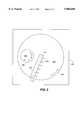
- FIG. 2is a top view of a CMP apparatus depicted according to the present invention.
- FIG. 3is a side view of slurry dispenser 210 depicted in accordance with a preferred embodiment of the present invention.
- FIG. 4is a cross-sectional view of a nozzle 214 depicted according to the present invention.
- CMPinvolves both chemical reaction and mechanical abrasion.
- Chemical reactionis accomplished using a slurry to chemically weaken the surface of a wafer.
- Mechanical abrasionis accomplished using a polishing pad against which a wafer surface is pressed in conjunction with abrasives in the slurry.
- both the polishing pad and the waferare rotated to cause the removal of surface material.
- the removed materialis then washed over the edges of the polishing pads and into a drain by adding additional slurry.
- CMP planarizationproduces a smooth, damage-free surface for subsequent device processing. It requires less steps than a deposition/etchback planarization and has good removal selectivity and rate control.
- For silicon dioxideremoval rates on the order of 50-300 nm/min for a thermal oxide and 55-330 nm/min for an LPCVD (low pressure chemical-vapor deposition) oxide can be achieved.
- CMP apparatus 200contains a polishing pad 202 attached to a rotating platen disk 204.
- Polishing pad 202typically comprises polyurethane. However, it will be apparent to those skilled in the art that other materials such as those used to make pads for glass polishing may be used. In addition, the hardness of polishing pad 202 may vary depending on the application. Wafer 206 is held on a rotating carrier 208 and pressed against polishing pad 202.
- CMP apparatus 200includes a slurry dispenser 210.
- Slurry dispenser 210is an elongate member in the depicted example.
- Slurry dispenser 210has a cavity within and an input 212 connected to a slurry source.
- slurry dispenser 210includes nozzles 214 shown in more detail in FIGS. 3 and 4, which provide an output for directing or spraying slurry at the polishing pad.
- each nozzlemay be directly connected to a slurry source.
- slurryhas been dripped onto the polishing pad at a rate from about 150 ml/min. to about 700 ml/min. The slurry would then be spread across the polishing pad through the spinning of the polishing pad.
- slurryis input into slurry dispenser 210 through input 212 at various pressures to generate slurry streams 216 having subsonic velocities to supersonic velocities that are directed by nozzles 214 onto the surface of the polishing pad 202 to remove embedded debris or materials to condition polishing pad 202, resulting in conditioning of polishing pad 202.
- Conditioning of the polishing padresults in removal of embedded debris and roughening of the surface of the polishing pad to receive new slurry.
- slurry from slurry streams 216coats the surface of polishing pad 202. By spraying slurry onto the polishing pad in the manner shown and described, a more uniform coating of slurry on polishing pad 202 is generated.
- the velocity of slurry streams 216is adjusted to provide enough kinetic energy to remove debris such as, for example, slurry particles and residual polished material from the surface of polishing pad 202. Additionally, the slurry particles in slurry streams 216 lose momentum and reside on the surface of polishing pad 202 and provide a new surface for polishing.
- the pressure of the slurry at input 212controls the velocity of slurry streams 216 out of slurry dispenser 210.
- a balance between removal of embedded debris and erosion of polishing pad 202is used to determine the velocity of slurry streams 216 generated by slurry dispenser 210. Typically, the velocity of the slurry streams 216 are adjusted to minimize pad erosion while providing removal of embedded debris.
- the slurry from the slurry streams 216also coats or covers polishing pad 202 with slurry for CMP.
- a typical slurry for interlevel dielectric planarizationcomprises silicon dioxide in a basic solution such as KOH (potassium hydroxide), which is diluted with water.
- KOHpotassium hydroxide
- Other slurry compositionswill be apparent to those of ordinary skill in the art.
- FIG. 3a side view of slurry dispenser 210 is depicted according to the present invention.
- Nozzles 214direct slurry streams 216 onto polishing pad 202.
- Nozzles 214may be positioned at various angles with respect to polishing pad 202 as can be seen in FIG. 3.
- FIG. 4a cross-sectional view of a nozzle 214 is depicted according to the present invention. As can be seen, nozzle 214 includes an input 400 for receiving slurry 402.
- slurry 402As slurry 402 is input into nozzle 214, it passes proximate to an ultrasonic energy source in the form of an ultrasonic or piezo transducer 404, which imparts ultrasonic energy to slurry 402 as it is sent through cavity 406 to form a slurry stream 216.
- Slurry stream 216energized with ultrasonic energy, is used to remove slurry particles and residual polished material from the surface of polishing pad 202 and roughen the surface to receive new slurry. Additionally, a coating of slurry remains on polishing pad 202 for CMP. End 408 of nozzle 214 is positioned at a distance X from pad 202.
- end 408 of nozzle 214is positioned from about 0.010 inches to about 0.100 inches from pad 202.
- the position of end 408is set to maximize the retention of kinetic energy in the slurry while minimizing erosion of pad 202.
- the combination of a high velocity slurry stream (from subsonic to supersonic velocities) and applied ultrasonic energyalso provides an improved method and apparatus for removing embedded debris while reducing erosion of the polishing pad.
- slurry dispenser 210includes a number of nozzles 214 arranged in an array fashion across the radius of polishing pad 202, slurry dispenser 210 may take on a number of other shapes. Using an inline approach, such as shown in slurry dispenser 210, the entire polishing pad is covered across the radius of the polishing pad. Alternatively, a dispenser in the form of a moveable arm with a single nozzle that can be moved over different portions of the polishing pad to condition the entire polishing pad may be employed according to the present invention.
- the nozzle size and shape and slurry pressure usedmay vary as long as the desired results are achieved, such as, for example, minimizing erosion of the polishing pad removing embedded debris, and providing a uniformed coating of slurry on the polishing pad.
- the resulting conditioning processis uniform across polishing pad 202, and nozzles 214 can be adjusted for high velocity slurry, low velocity slurry, ultrasonic slurry, or a combination such as high velocity slurry with ultrasonic energy.
- the present inventionprovides an improved method and apparatus for conditioning a polishing pad without requiring contact by a grid with the polishing pad, resulting in reduced erosion of the polishing pad.
- This featurealso may be used for the delivery of low pH slurries because many grids become corroded from low pH solutions.
- the present inventionreduces the need for grids to condition the polishing pad and provides uniform conditioning of the polishing pad resulting in improved wafer uniformity and stable removal rates in the CMP processing.
- the present inventionprovides an advantage over presently known systems because the slurry dispenser provides for a uniform coating of slurry on the polishing pad in addition to conditioning the polishing pad.
- the present inventionprovides increased longevity of the polishing pad by reducing the erosion within the polishing pad.
- dispenser 210extends across the radius of polishing pad 202 in FIG. 2
- a slurry dispenser extending across a diameter of polishing pad 202also could be implemented in accordance with a preferred embodiments of the present invention without departing from the spirit and scope of the invention.
Landscapes
- Engineering & Computer Science (AREA)
- Mechanical Engineering (AREA)
- Mechanical Treatment Of Semiconductor (AREA)
- Grinding-Machine Dressing And Accessory Apparatuses (AREA)
- Finish Polishing, Edge Sharpening, And Grinding By Specific Grinding Devices (AREA)
Abstract
Description
Claims (13)
Priority Applications (6)
| Application Number | Priority Date | Filing Date | Title |
|---|---|---|---|
| US08/696,445US5868608A (en) | 1996-08-13 | 1996-08-13 | Subsonic to supersonic and ultrasonic conditioning of a polishing pad in a chemical mechanical polishing apparatus |
| EP97931917AEP0921904B1 (en) | 1996-08-13 | 1997-07-15 | Apparatus and method for polishing semiconductor devices |
| PCT/GB1997/001894WO1998006540A1 (en) | 1996-08-13 | 1997-07-15 | Apparatus and method for polishing semiconductor devices |
| DE69709934TDE69709934T2 (en) | 1996-08-13 | 1997-07-15 | METHOD AND DEVICE FOR POLISHING SEMICONDUCTOR DISCS |
| AU35505/97AAU3550597A (en) | 1996-08-13 | 1997-07-15 | Apparatus and method for polishing semiconductor devices |
| US09/211,024US6168502B1 (en) | 1996-08-13 | 1998-12-14 | Subsonic to supersonic and ultrasonic conditioning of a polishing pad in a chemical mechanical polishing apparatus |
Applications Claiming Priority (1)
| Application Number | Priority Date | Filing Date | Title |
|---|---|---|---|
| US08/696,445US5868608A (en) | 1996-08-13 | 1996-08-13 | Subsonic to supersonic and ultrasonic conditioning of a polishing pad in a chemical mechanical polishing apparatus |
Related Child Applications (1)
| Application Number | Title | Priority Date | Filing Date |
|---|---|---|---|
| US09/211,024DivisionUS6168502B1 (en) | 1996-08-13 | 1998-12-14 | Subsonic to supersonic and ultrasonic conditioning of a polishing pad in a chemical mechanical polishing apparatus |
Publications (1)
| Publication Number | Publication Date |
|---|---|
| US5868608Atrue US5868608A (en) | 1999-02-09 |
Family
ID=24797095
Family Applications (2)
| Application Number | Title | Priority Date | Filing Date |
|---|---|---|---|
| US08/696,445Expired - LifetimeUS5868608A (en) | 1996-08-13 | 1996-08-13 | Subsonic to supersonic and ultrasonic conditioning of a polishing pad in a chemical mechanical polishing apparatus |
| US09/211,024Expired - LifetimeUS6168502B1 (en) | 1996-08-13 | 1998-12-14 | Subsonic to supersonic and ultrasonic conditioning of a polishing pad in a chemical mechanical polishing apparatus |
Family Applications After (1)
| Application Number | Title | Priority Date | Filing Date |
|---|---|---|---|
| US09/211,024Expired - LifetimeUS6168502B1 (en) | 1996-08-13 | 1998-12-14 | Subsonic to supersonic and ultrasonic conditioning of a polishing pad in a chemical mechanical polishing apparatus |
Country Status (5)
| Country | Link |
|---|---|
| US (2) | US5868608A (en) |
| EP (1) | EP0921904B1 (en) |
| AU (1) | AU3550597A (en) |
| DE (1) | DE69709934T2 (en) |
| WO (1) | WO1998006540A1 (en) |
Cited By (51)
| Publication number | Priority date | Publication date | Assignee | Title |
|---|---|---|---|---|
| US5957757A (en)* | 1997-10-30 | 1999-09-28 | Lsi Logic Corporation | Conditioning CMP polishing pad using a high pressure fluid |
| US6060370A (en)* | 1998-06-16 | 2000-05-09 | Lsi Logic Corporation | Method for shallow trench isolations with chemical-mechanical polishing |
| US6066266A (en)* | 1998-07-08 | 2000-05-23 | Lsi Logic Corporation | In-situ chemical-mechanical polishing slurry formulation for compensation of polish pad degradation |
| US6071818A (en)* | 1998-06-30 | 2000-06-06 | Lsi Logic Corporation | Endpoint detection method and apparatus which utilize an endpoint polishing layer of catalyst material |
| US6074517A (en)* | 1998-07-08 | 2000-06-13 | Lsi Logic Corporation | Method and apparatus for detecting an endpoint polishing layer by transmitting infrared light signals through a semiconductor wafer |
| US6077783A (en)* | 1998-06-30 | 2000-06-20 | Lsi Logic Corporation | Method and apparatus for detecting a polishing endpoint based upon heat conducted through a semiconductor wafer |
| US6080670A (en)* | 1998-08-10 | 2000-06-27 | Lsi Logic Corporation | Method of detecting a polishing endpoint layer of a semiconductor wafer which includes a non-reactive reporting specie |
| US6083085A (en)* | 1997-12-22 | 2000-07-04 | Micron Technology, Inc. | Method and apparatus for planarizing microelectronic substrates and conditioning planarizing media |
| US6093280A (en)* | 1997-08-18 | 2000-07-25 | Lsi Logic Corporation | Chemical-mechanical polishing pad conditioning systems |
| US6106371A (en)* | 1997-10-30 | 2000-08-22 | Lsi Logic Corporation | Effective pad conditioning |
| US6108093A (en)* | 1997-06-04 | 2000-08-22 | Lsi Logic Corporation | Automated inspection system for residual metal after chemical-mechanical polishing |
| US6115233A (en)* | 1996-06-28 | 2000-09-05 | Lsi Logic Corporation | Integrated circuit device having a capacitor with the dielectric peripheral region being greater than the dielectric central region |
| US6117779A (en)* | 1998-12-15 | 2000-09-12 | Lsi Logic Corporation | Endpoint detection method and apparatus which utilize a chelating agent to detect a polishing endpoint |
| US6121147A (en)* | 1998-12-11 | 2000-09-19 | Lsi Logic Corporation | Apparatus and method of detecting a polishing endpoint layer of a semiconductor wafer which includes a metallic reporting substance |
| US6168508B1 (en) | 1997-08-25 | 2001-01-02 | Lsi Logic Corporation | Polishing pad surface for improved process control |
| US6179956B1 (en) | 1998-01-09 | 2001-01-30 | Lsi Logic Corporation | Method and apparatus for using across wafer back pressure differentials to influence the performance of chemical mechanical polishing |
| US6201253B1 (en) | 1998-10-22 | 2001-03-13 | Lsi Logic Corporation | Method and apparatus for detecting a planarized outer layer of a semiconductor wafer with a confocal optical system |
| US6234883B1 (en) | 1997-10-01 | 2001-05-22 | Lsi Logic Corporation | Method and apparatus for concurrent pad conditioning and wafer buff in chemical mechanical polishing |
| US6241587B1 (en)* | 1998-02-13 | 2001-06-05 | Vlsi Technology, Inc. | System for dislodging by-product agglomerations from a polishing pad of a chemical mechanical polishing machine |
| US6241847B1 (en) | 1998-06-30 | 2001-06-05 | Lsi Logic Corporation | Method and apparatus for detecting a polishing endpoint based upon infrared signals |
| US6268224B1 (en) | 1998-06-30 | 2001-07-31 | Lsi Logic Corporation | Method and apparatus for detecting an ion-implanted polishing endpoint layer within a semiconductor wafer |
| US6285035B1 (en) | 1998-07-08 | 2001-09-04 | Lsi Logic Corporation | Apparatus for detecting an endpoint polishing layer of a semiconductor wafer having a wafer carrier with independent concentric sub-carriers and associated method |
| WO2001017724A3 (en)* | 1999-09-07 | 2001-09-27 | Philips Semiconductors Inc | Ultrasonic transducer slurry dispenser |
| US6297558B1 (en) | 1997-07-23 | 2001-10-02 | Lsi Logic Corporation | Slurry filling a recess formed during semiconductor fabrication |
| GB2360725A (en)* | 2000-01-05 | 2001-10-03 | Lucent Technologies Inc | Method of conditioning a pad for a chemical mechanical polisher |
| US6302771B1 (en)* | 1999-04-01 | 2001-10-16 | Philips Semiconductor, Inc. | CMP pad conditioner arrangement and method therefor |
| US6319836B1 (en) | 2000-09-26 | 2001-11-20 | Lsi Logic Corporation | Planarization system |
| US6331136B1 (en)* | 2000-01-25 | 2001-12-18 | Koninklijke Philips Electronics N.V. (Kpenv) | CMP pad conditioner arrangement and method therefor |
| US6336850B1 (en)* | 1997-10-15 | 2002-01-08 | Ebara Corporation | Slurry dispenser and polishing apparatus |
| US6340434B1 (en) | 1997-09-05 | 2002-01-22 | Lsi Logic Corporation | Method and apparatus for chemical-mechanical polishing |
| US6350183B2 (en)* | 1999-08-10 | 2002-02-26 | International Business Machines Corporation | High pressure cleaning |
| US6375550B1 (en) | 2000-06-05 | 2002-04-23 | Lsi Logic Corporation | Method and apparatus for enhancing uniformity during polishing of a semiconductor wafer |
| US6391768B1 (en) | 2000-10-30 | 2002-05-21 | Lsi Logic Corporation | Process for CMP removal of excess trench or via filler metal which inhibits formation of concave regions on oxide surface of integrated circuit structure |
| US6429131B2 (en)* | 1999-03-18 | 2002-08-06 | Infineon Technologies Ag | CMP uniformity |
| US6439981B1 (en) | 2000-12-28 | 2002-08-27 | Lsi Logic Corporation | Arrangement and method for polishing a surface of a semiconductor wafer |
| US6451699B1 (en) | 1999-07-30 | 2002-09-17 | Lsi Logic Corporation | Method and apparatus for planarizing a wafer surface of a semiconductor wafer having an elevated portion extending therefrom |
| US6464566B1 (en) | 2000-06-29 | 2002-10-15 | Lsi Logic Corporation | Apparatus and method for linearly planarizing a surface of a semiconductor wafer |
| US6489242B1 (en) | 2000-09-13 | 2002-12-03 | Lsi Logic Corporation | Process for planarization of integrated circuit structure which inhibits cracking of low dielectric constant dielectric material adjacent underlying raised structures |
| US6528389B1 (en) | 1998-12-17 | 2003-03-04 | Lsi Logic Corporation | Substrate planarization with a chemical mechanical polishing stop layer |
| DE10162965A1 (en)* | 2000-12-20 | 2003-03-27 | Nsk Ltd | Rolling bearing and bearing unit |
| US6541383B1 (en) | 2000-06-29 | 2003-04-01 | Lsi Logic Corporation | Apparatus and method for planarizing the surface of a semiconductor wafer |
| US20030073391A1 (en)* | 2001-07-24 | 2003-04-17 | Janzen John W. | Ultrasonic conditioning device cleaner for chemical mechanical polishing systems |
| US6607967B1 (en) | 2000-11-15 | 2003-08-19 | Lsi Logic Corporation | Process for forming planarized isolation trench in integrated circuit structure on semiconductor substrate |
| US6705930B2 (en) | 2000-01-28 | 2004-03-16 | Lam Research Corporation | System and method for polishing and planarizing semiconductor wafers using reduced surface area polishing pads and variable partial pad-wafer overlapping techniques |
| US6729943B2 (en) | 2000-01-28 | 2004-05-04 | Lam Research Corporation | System and method for controlled polishing and planarization of semiconductor wafers |
| US20040116051A1 (en)* | 2001-08-30 | 2004-06-17 | Kramer Stephen J. | Method and apparatus for conditioning a chemical-mechanical polishing pad |
| US6896600B1 (en)* | 2002-03-29 | 2005-05-24 | Lam Research Corporation | Liquid dispense manifold for chemical-mechanical polisher |
| US7751609B1 (en) | 2000-04-20 | 2010-07-06 | Lsi Logic Corporation | Determination of film thickness during chemical mechanical polishing |
| US20130210323A1 (en)* | 2012-02-15 | 2013-08-15 | Taiwan Semiconductor Manufacturing Co., Ltd. | CMP Pad Cleaning Apparatus |
| US20170297163A1 (en)* | 2013-01-11 | 2017-10-19 | Applied Materials, Inc. | Chemical mechanical polishing apparatus and methods |
| US20230178388A1 (en)* | 2021-12-03 | 2023-06-08 | Applied Materials, Inc. | Surface cleaning with directed high pressure chemistry |
Families Citing this family (15)
| Publication number | Priority date | Publication date | Assignee | Title |
|---|---|---|---|---|
| WO1999029505A1 (en)* | 1997-12-08 | 1999-06-17 | Ebara Corporation | Polishing solution feeder |
| US5957754A (en)* | 1997-08-29 | 1999-09-28 | Applied Materials, Inc. | Cavitational polishing pad conditioner |
| JP2000033555A (en)* | 1998-07-17 | 2000-02-02 | Sony Corp | Polishing device |
| JP2001212750A (en)* | 1999-11-25 | 2001-08-07 | Fujikoshi Mach Corp | Polishing machine cleaning equipment and polishing machine |
| US6669538B2 (en)* | 2000-02-24 | 2003-12-30 | Applied Materials Inc | Pad cleaning for a CMP system |
| US6875091B2 (en)* | 2001-01-04 | 2005-04-05 | Lam Research Corporation | Method and apparatus for conditioning a polishing pad with sonic energy |
| JP2002307312A (en)* | 2001-04-11 | 2002-10-23 | Olympus Optical Co Ltd | Polishing device, polishing method, control program for letting computer execute polishing, and recording medium |
| US6764388B2 (en)* | 2002-05-09 | 2004-07-20 | Taiwan Semiconductor Manufacturing Co., Ltd | High-pressure pad cleaning system |
| DE10261465B4 (en)* | 2002-12-31 | 2013-03-21 | Advanced Micro Devices, Inc. | Arrangement for chemical mechanical polishing with an improved conditioning tool |
| US20060073773A1 (en)* | 2004-10-04 | 2006-04-06 | Exley Richard J | High pressure pad conditioning |
| US20070066187A1 (en)* | 2005-09-22 | 2007-03-22 | Chih-Chiang Yang | Chemical mechanical polishing device including a polishing pad and cleaning method thereof and method for planarization |
| RU2305621C1 (en)* | 2005-11-29 | 2007-09-10 | Государственное образовательное учреждение высшего профессионального образования "Алтайский государственный технический университет им. И.И. Ползунова" (АлтГТУ) | Chemical - mechanical polishing method |
| JP2010228058A (en)* | 2009-03-27 | 2010-10-14 | Fujikoshi Mach Corp | Polishing cloth cleaning apparatus and cleaning method |
| CN102553849B (en)* | 2010-12-29 | 2015-04-29 | 中芯国际集成电路制造(上海)有限公司 | Cleaning device and cleaning method for fixed grinding particle polishing pad |
| KR20220073192A (en)* | 2020-11-26 | 2022-06-03 | 에스케이실트론 주식회사 | Apparatus of cleaning a polishing pad and polishing device |
Citations (37)
| Publication number | Priority date | Publication date | Assignee | Title |
|---|---|---|---|---|
| US2774194A (en)* | 1954-11-08 | 1956-12-18 | Charles J Thatcher | Ultrasonic tools |
| US3091060A (en)* | 1957-07-12 | 1963-05-28 | Lehfeldt & Company G M B H Dr | Ultrasonic machining |
| US3093937A (en)* | 1962-11-30 | 1963-06-18 | Cavitron Ultrasonics Inc | Ultrasonic lapping machines |
| US3094814A (en)* | 1960-11-21 | 1963-06-25 | Barke Vladimir Nikolaevich | Ultrasonic abrasive machining apparatus |
| US3123950A (en)* | 1964-03-10 | Ultrasonic cleaning of grinding wheels | ||
| US3123951A (en)* | 1964-03-10 | Ultrasonic cleaning of grinding wheels | ||
| US3167893A (en)* | 1962-11-05 | 1965-02-02 | Sheffield Corp | Apparatus for cleaning grinding wheels |
| US3500591A (en)* | 1966-11-21 | 1970-03-17 | Owens Illinois Inc | Glass grinding method and apparatus |
| US3568377A (en)* | 1968-01-09 | 1971-03-09 | Robert Blohm | Device for cooling and cleaning of grinding wheels |
| US3638366A (en)* | 1969-12-03 | 1972-02-01 | Norton Co | Lapping method for metallic workpieces |
| US3812622A (en)* | 1972-06-14 | 1974-05-28 | J Parsons | Sander cleaner |
| US3848366A (en)* | 1973-01-16 | 1974-11-19 | J David | Means to assure uniform flow of an abrasive solution |
| US4004375A (en)* | 1974-07-25 | 1977-01-25 | Supfina Maschinenfabrik Hentzen Kg | Apparatus for continuous cleaning of a honing tool |
| US4059929A (en)* | 1976-05-10 | 1977-11-29 | Chemical-Ways Corporation | Precision metering system for the delivery of abrasive lapping and polishing slurries |
| DE3007709A1 (en)* | 1980-02-29 | 1981-10-01 | Gleitlagertechnik Gmbh, 7000 Stuttgart | DEVICE FOR FEEDING COOLANT IN TOOLS |
| US4326553A (en)* | 1980-08-28 | 1982-04-27 | Rca Corporation | Megasonic jet cleaner apparatus |
| JPH0310769A (en)* | 1989-06-05 | 1991-01-18 | Mitsubishi Materials Corp | Dressing device for polishing cloth |
| US5154021A (en)* | 1991-06-26 | 1992-10-13 | International Business Machines Corporation | Pneumatic pad conditioner |
| US5168671A (en)* | 1989-05-30 | 1992-12-08 | Fuji Seiki Machine Works, Ltd. | Dressing method and apparatus for super abrasive grinding wheel |
| US5216843A (en)* | 1992-09-24 | 1993-06-08 | Intel Corporation | Polishing pad conditioning apparatus for wafer planarization process |
| US5245790A (en)* | 1992-02-14 | 1993-09-21 | Lsi Logic Corporation | Ultrasonic energy enhanced chemi-mechanical polishing of silicon wafers |
| US5245796A (en)* | 1992-04-02 | 1993-09-21 | At&T Bell Laboratories | Slurry polisher using ultrasonic agitation |
| US5291693A (en)* | 1992-08-20 | 1994-03-08 | Texas Instruments Incorporated | Semiconductors structure precision lapping method and system |
| US5345639A (en)* | 1992-05-28 | 1994-09-13 | Tokyo Electron Limited | Device and method for scrubbing and cleaning substrate |
| US5399234A (en)* | 1993-09-29 | 1995-03-21 | Motorola Inc. | Acoustically regulated polishing process |
| DE4334391A1 (en)* | 1993-10-08 | 1995-05-04 | Ppv Verwaltungs Ag | Method and apparatus for working a surface of a workpiece |
| JP3010769U (en) | 1994-11-01 | 1995-05-09 | 多摩川精機株式会社 | Copying device |
| US5421768A (en)* | 1993-06-30 | 1995-06-06 | Mitsubishi Materials Corporation | Abrasive cloth dresser |
| US5421769A (en)* | 1990-01-22 | 1995-06-06 | Micron Technology, Inc. | Apparatus for planarizing semiconductor wafers, and a polishing pad for a planarization apparatus |
| US5522965A (en)* | 1994-12-12 | 1996-06-04 | Texas Instruments Incorporated | Compact system and method for chemical-mechanical polishing utilizing energy coupled to the polishing pad/water interface |
| US5551907A (en)* | 1994-03-14 | 1996-09-03 | Hughes Aircraft Company | System for ultrasonic lap grinding and polishing |
| US5584749A (en)* | 1995-01-13 | 1996-12-17 | Nec Corporation | Surface polishing apparatus |
| US5616069A (en)* | 1995-12-19 | 1997-04-01 | Micron Technology, Inc. | Directional spray pad scrubber |
| US5626509A (en)* | 1994-03-16 | 1997-05-06 | Nec Corporation | Surface treatment of polishing cloth |
| US5643067A (en)* | 1994-12-16 | 1997-07-01 | Ebara Corporation | Dressing apparatus and method |
| US5645682A (en)* | 1996-05-28 | 1997-07-08 | Micron Technology, Inc. | Apparatus and method for conditioning a planarizing substrate used in chemical-mechanical planarization of semiconductor wafers |
| US5725417A (en)* | 1996-11-05 | 1998-03-10 | Micron Technology, Inc. | Method and apparatus for conditioning polishing pads used in mechanical and chemical-mechanical planarization of substrates |
Family Cites Families (2)
| Publication number | Priority date | Publication date | Assignee | Title |
|---|---|---|---|---|
| SU1240561A1 (en)* | 1984-11-28 | 1986-06-30 | Московский автомеханический институт | Method of cleaning abrasive wheel when grinding ferromagnetic materials |
| JP3010769B2 (en) | 1991-04-11 | 2000-02-21 | 三菱電機株式会社 | Method and apparatus for assembling optical element module |
- 1996
- 1996-08-13USUS08/696,445patent/US5868608A/ennot_activeExpired - Lifetime
- 1997
- 1997-07-15EPEP97931917Apatent/EP0921904B1/ennot_activeExpired - Lifetime
- 1997-07-15AUAU35505/97Apatent/AU3550597A/ennot_activeAbandoned
- 1997-07-15DEDE69709934Tpatent/DE69709934T2/ennot_activeExpired - Lifetime
- 1997-07-15WOPCT/GB1997/001894patent/WO1998006540A1/enactiveIP Right Grant
- 1998
- 1998-12-14USUS09/211,024patent/US6168502B1/ennot_activeExpired - Lifetime
Patent Citations (37)
| Publication number | Priority date | Publication date | Assignee | Title |
|---|---|---|---|---|
| US3123950A (en)* | 1964-03-10 | Ultrasonic cleaning of grinding wheels | ||
| US3123951A (en)* | 1964-03-10 | Ultrasonic cleaning of grinding wheels | ||
| US2774194A (en)* | 1954-11-08 | 1956-12-18 | Charles J Thatcher | Ultrasonic tools |
| US3091060A (en)* | 1957-07-12 | 1963-05-28 | Lehfeldt & Company G M B H Dr | Ultrasonic machining |
| US3094814A (en)* | 1960-11-21 | 1963-06-25 | Barke Vladimir Nikolaevich | Ultrasonic abrasive machining apparatus |
| US3167893A (en)* | 1962-11-05 | 1965-02-02 | Sheffield Corp | Apparatus for cleaning grinding wheels |
| US3093937A (en)* | 1962-11-30 | 1963-06-18 | Cavitron Ultrasonics Inc | Ultrasonic lapping machines |
| US3500591A (en)* | 1966-11-21 | 1970-03-17 | Owens Illinois Inc | Glass grinding method and apparatus |
| US3568377A (en)* | 1968-01-09 | 1971-03-09 | Robert Blohm | Device for cooling and cleaning of grinding wheels |
| US3638366A (en)* | 1969-12-03 | 1972-02-01 | Norton Co | Lapping method for metallic workpieces |
| US3812622A (en)* | 1972-06-14 | 1974-05-28 | J Parsons | Sander cleaner |
| US3848366A (en)* | 1973-01-16 | 1974-11-19 | J David | Means to assure uniform flow of an abrasive solution |
| US4004375A (en)* | 1974-07-25 | 1977-01-25 | Supfina Maschinenfabrik Hentzen Kg | Apparatus for continuous cleaning of a honing tool |
| US4059929A (en)* | 1976-05-10 | 1977-11-29 | Chemical-Ways Corporation | Precision metering system for the delivery of abrasive lapping and polishing slurries |
| DE3007709A1 (en)* | 1980-02-29 | 1981-10-01 | Gleitlagertechnik Gmbh, 7000 Stuttgart | DEVICE FOR FEEDING COOLANT IN TOOLS |
| US4326553A (en)* | 1980-08-28 | 1982-04-27 | Rca Corporation | Megasonic jet cleaner apparatus |
| US5168671A (en)* | 1989-05-30 | 1992-12-08 | Fuji Seiki Machine Works, Ltd. | Dressing method and apparatus for super abrasive grinding wheel |
| JPH0310769A (en)* | 1989-06-05 | 1991-01-18 | Mitsubishi Materials Corp | Dressing device for polishing cloth |
| US5421769A (en)* | 1990-01-22 | 1995-06-06 | Micron Technology, Inc. | Apparatus for planarizing semiconductor wafers, and a polishing pad for a planarization apparatus |
| US5154021A (en)* | 1991-06-26 | 1992-10-13 | International Business Machines Corporation | Pneumatic pad conditioner |
| US5245790A (en)* | 1992-02-14 | 1993-09-21 | Lsi Logic Corporation | Ultrasonic energy enhanced chemi-mechanical polishing of silicon wafers |
| US5245796A (en)* | 1992-04-02 | 1993-09-21 | At&T Bell Laboratories | Slurry polisher using ultrasonic agitation |
| US5345639A (en)* | 1992-05-28 | 1994-09-13 | Tokyo Electron Limited | Device and method for scrubbing and cleaning substrate |
| US5291693A (en)* | 1992-08-20 | 1994-03-08 | Texas Instruments Incorporated | Semiconductors structure precision lapping method and system |
| US5216843A (en)* | 1992-09-24 | 1993-06-08 | Intel Corporation | Polishing pad conditioning apparatus for wafer planarization process |
| US5421768A (en)* | 1993-06-30 | 1995-06-06 | Mitsubishi Materials Corporation | Abrasive cloth dresser |
| US5399234A (en)* | 1993-09-29 | 1995-03-21 | Motorola Inc. | Acoustically regulated polishing process |
| DE4334391A1 (en)* | 1993-10-08 | 1995-05-04 | Ppv Verwaltungs Ag | Method and apparatus for working a surface of a workpiece |
| US5551907A (en)* | 1994-03-14 | 1996-09-03 | Hughes Aircraft Company | System for ultrasonic lap grinding and polishing |
| US5626509A (en)* | 1994-03-16 | 1997-05-06 | Nec Corporation | Surface treatment of polishing cloth |
| JP3010769U (en) | 1994-11-01 | 1995-05-09 | 多摩川精機株式会社 | Copying device |
| US5522965A (en)* | 1994-12-12 | 1996-06-04 | Texas Instruments Incorporated | Compact system and method for chemical-mechanical polishing utilizing energy coupled to the polishing pad/water interface |
| US5643067A (en)* | 1994-12-16 | 1997-07-01 | Ebara Corporation | Dressing apparatus and method |
| US5584749A (en)* | 1995-01-13 | 1996-12-17 | Nec Corporation | Surface polishing apparatus |
| US5616069A (en)* | 1995-12-19 | 1997-04-01 | Micron Technology, Inc. | Directional spray pad scrubber |
| US5645682A (en)* | 1996-05-28 | 1997-07-08 | Micron Technology, Inc. | Apparatus and method for conditioning a planarizing substrate used in chemical-mechanical planarization of semiconductor wafers |
| US5725417A (en)* | 1996-11-05 | 1998-03-10 | Micron Technology, Inc. | Method and apparatus for conditioning polishing pads used in mechanical and chemical-mechanical planarization of substrates |
Non-Patent Citations (2)
| Title |
|---|
| Database WPI; Section PQ, Week 8708; Derwent Publications Ltd., London, GB; Class P61, AN 87 055121, XP002045272 and SU 1 240 561 A (MOSC Automech Inst); Jun. 30, 1986.* |
| Database WPI; Section PQ, Week 8708; Derwent Publications Ltd., London, GB; Class P61, AN 87-055121, XP002045272 and SU 1 240 561 A (MOSC Automech Inst); Jun. 30, 1986. |
Cited By (77)
| Publication number | Priority date | Publication date | Assignee | Title |
|---|---|---|---|---|
| US6115233A (en)* | 1996-06-28 | 2000-09-05 | Lsi Logic Corporation | Integrated circuit device having a capacitor with the dielectric peripheral region being greater than the dielectric central region |
| US6108093A (en)* | 1997-06-04 | 2000-08-22 | Lsi Logic Corporation | Automated inspection system for residual metal after chemical-mechanical polishing |
| US6297558B1 (en) | 1997-07-23 | 2001-10-02 | Lsi Logic Corporation | Slurry filling a recess formed during semiconductor fabrication |
| US6093280A (en)* | 1997-08-18 | 2000-07-25 | Lsi Logic Corporation | Chemical-mechanical polishing pad conditioning systems |
| US6168508B1 (en) | 1997-08-25 | 2001-01-02 | Lsi Logic Corporation | Polishing pad surface for improved process control |
| US6340434B1 (en) | 1997-09-05 | 2002-01-22 | Lsi Logic Corporation | Method and apparatus for chemical-mechanical polishing |
| US6234883B1 (en) | 1997-10-01 | 2001-05-22 | Lsi Logic Corporation | Method and apparatus for concurrent pad conditioning and wafer buff in chemical mechanical polishing |
| US6336850B1 (en)* | 1997-10-15 | 2002-01-08 | Ebara Corporation | Slurry dispenser and polishing apparatus |
| US6106371A (en)* | 1997-10-30 | 2000-08-22 | Lsi Logic Corporation | Effective pad conditioning |
| US5957757A (en)* | 1997-10-30 | 1999-09-28 | Lsi Logic Corporation | Conditioning CMP polishing pad using a high pressure fluid |
| US6083085A (en)* | 1997-12-22 | 2000-07-04 | Micron Technology, Inc. | Method and apparatus for planarizing microelectronic substrates and conditioning planarizing media |
| US6354923B1 (en) | 1997-12-22 | 2002-03-12 | Micron Technology, Inc. | Apparatus for planarizing microelectronic substrates and conditioning planarizing media |
| US6350691B1 (en)* | 1997-12-22 | 2002-02-26 | Micron Technology, Inc. | Method and apparatus for planarizing microelectronic substrates and conditioning planarizing media |
| US6531397B1 (en) | 1998-01-09 | 2003-03-11 | Lsi Logic Corporation | Method and apparatus for using across wafer back pressure differentials to influence the performance of chemical mechanical polishing |
| US6179956B1 (en) | 1998-01-09 | 2001-01-30 | Lsi Logic Corporation | Method and apparatus for using across wafer back pressure differentials to influence the performance of chemical mechanical polishing |
| US6241587B1 (en)* | 1998-02-13 | 2001-06-05 | Vlsi Technology, Inc. | System for dislodging by-product agglomerations from a polishing pad of a chemical mechanical polishing machine |
| US6424019B1 (en) | 1998-06-16 | 2002-07-23 | Lsi Logic Corporation | Shallow trench isolation chemical-mechanical polishing process |
| US6060370A (en)* | 1998-06-16 | 2000-05-09 | Lsi Logic Corporation | Method for shallow trench isolations with chemical-mechanical polishing |
| US6241847B1 (en) | 1998-06-30 | 2001-06-05 | Lsi Logic Corporation | Method and apparatus for detecting a polishing endpoint based upon infrared signals |
| US6071818A (en)* | 1998-06-30 | 2000-06-06 | Lsi Logic Corporation | Endpoint detection method and apparatus which utilize an endpoint polishing layer of catalyst material |
| US6258205B1 (en) | 1998-06-30 | 2001-07-10 | Lsi Logic Corporation | Endpoint detection method and apparatus which utilize an endpoint polishing layer of catalyst material |
| US6268224B1 (en) | 1998-06-30 | 2001-07-31 | Lsi Logic Corporation | Method and apparatus for detecting an ion-implanted polishing endpoint layer within a semiconductor wafer |
| US6077783A (en)* | 1998-06-30 | 2000-06-20 | Lsi Logic Corporation | Method and apparatus for detecting a polishing endpoint based upon heat conducted through a semiconductor wafer |
| US6285035B1 (en) | 1998-07-08 | 2001-09-04 | Lsi Logic Corporation | Apparatus for detecting an endpoint polishing layer of a semiconductor wafer having a wafer carrier with independent concentric sub-carriers and associated method |
| US6074517A (en)* | 1998-07-08 | 2000-06-13 | Lsi Logic Corporation | Method and apparatus for detecting an endpoint polishing layer by transmitting infrared light signals through a semiconductor wafer |
| US6066266A (en)* | 1998-07-08 | 2000-05-23 | Lsi Logic Corporation | In-situ chemical-mechanical polishing slurry formulation for compensation of polish pad degradation |
| US6080670A (en)* | 1998-08-10 | 2000-06-27 | Lsi Logic Corporation | Method of detecting a polishing endpoint layer of a semiconductor wafer which includes a non-reactive reporting specie |
| US6201253B1 (en) | 1998-10-22 | 2001-03-13 | Lsi Logic Corporation | Method and apparatus for detecting a planarized outer layer of a semiconductor wafer with a confocal optical system |
| US6354908B2 (en) | 1998-10-22 | 2002-03-12 | Lsi Logic Corp. | Method and apparatus for detecting a planarized outer layer of a semiconductor wafer with a confocal optical system |
| US6121147A (en)* | 1998-12-11 | 2000-09-19 | Lsi Logic Corporation | Apparatus and method of detecting a polishing endpoint layer of a semiconductor wafer which includes a metallic reporting substance |
| US6383332B1 (en) | 1998-12-15 | 2002-05-07 | Lsi Logic Corporation | Endpoint detection method and apparatus which utilize a chelating agent to detect a polishing endpoint |
| US6117779A (en)* | 1998-12-15 | 2000-09-12 | Lsi Logic Corporation | Endpoint detection method and apparatus which utilize a chelating agent to detect a polishing endpoint |
| US6528389B1 (en) | 1998-12-17 | 2003-03-04 | Lsi Logic Corporation | Substrate planarization with a chemical mechanical polishing stop layer |
| US6429131B2 (en)* | 1999-03-18 | 2002-08-06 | Infineon Technologies Ag | CMP uniformity |
| US6302771B1 (en)* | 1999-04-01 | 2001-10-16 | Philips Semiconductor, Inc. | CMP pad conditioner arrangement and method therefor |
| US6451699B1 (en) | 1999-07-30 | 2002-09-17 | Lsi Logic Corporation | Method and apparatus for planarizing a wafer surface of a semiconductor wafer having an elevated portion extending therefrom |
| US6350183B2 (en)* | 1999-08-10 | 2002-02-26 | International Business Machines Corporation | High pressure cleaning |
| WO2001017724A3 (en)* | 1999-09-07 | 2001-09-27 | Philips Semiconductors Inc | Ultrasonic transducer slurry dispenser |
| GB2360725A (en)* | 2000-01-05 | 2001-10-03 | Lucent Technologies Inc | Method of conditioning a pad for a chemical mechanical polisher |
| US6517416B1 (en) | 2000-01-05 | 2003-02-11 | Agere Systems Inc. | Chemical mechanical polisher including a pad conditioner and a method of manufacturing an integrated circuit using the chemical mechanical polisher |
| US6331136B1 (en)* | 2000-01-25 | 2001-12-18 | Koninklijke Philips Electronics N.V. (Kpenv) | CMP pad conditioner arrangement and method therefor |
| US6729943B2 (en) | 2000-01-28 | 2004-05-04 | Lam Research Corporation | System and method for controlled polishing and planarization of semiconductor wafers |
| US6705930B2 (en) | 2000-01-28 | 2004-03-16 | Lam Research Corporation | System and method for polishing and planarizing semiconductor wafers using reduced surface area polishing pads and variable partial pad-wafer overlapping techniques |
| US20040166782A1 (en)* | 2000-01-28 | 2004-08-26 | Lam Research Corporation. | System and method for polishing and planarizing semiconductor wafers using reduced surface area polishing pads and variable partial pad-wafer overlapping techniques |
| US6869337B2 (en) | 2000-01-28 | 2005-03-22 | Lam Research Corporation | System and method for polishing and planarizing semiconductor wafers using reduced surface area polishing pads and variable partial pad-wafer overlapping techniques |
| US7751609B1 (en) | 2000-04-20 | 2010-07-06 | Lsi Logic Corporation | Determination of film thickness during chemical mechanical polishing |
| US6375550B1 (en) | 2000-06-05 | 2002-04-23 | Lsi Logic Corporation | Method and apparatus for enhancing uniformity during polishing of a semiconductor wafer |
| US6541383B1 (en) | 2000-06-29 | 2003-04-01 | Lsi Logic Corporation | Apparatus and method for planarizing the surface of a semiconductor wafer |
| US6464566B1 (en) | 2000-06-29 | 2002-10-15 | Lsi Logic Corporation | Apparatus and method for linearly planarizing a surface of a semiconductor wafer |
| US6489242B1 (en) | 2000-09-13 | 2002-12-03 | Lsi Logic Corporation | Process for planarization of integrated circuit structure which inhibits cracking of low dielectric constant dielectric material adjacent underlying raised structures |
| US6713394B2 (en) | 2000-09-13 | 2004-03-30 | Lsi Logic Corporation | Process for planarization of integrated circuit structure which inhibits cracking of low dielectric constant dielectric material adjacent underlying raised structures |
| US6319836B1 (en) | 2000-09-26 | 2001-11-20 | Lsi Logic Corporation | Planarization system |
| US6391768B1 (en) | 2000-10-30 | 2002-05-21 | Lsi Logic Corporation | Process for CMP removal of excess trench or via filler metal which inhibits formation of concave regions on oxide surface of integrated circuit structure |
| US6607967B1 (en) | 2000-11-15 | 2003-08-19 | Lsi Logic Corporation | Process for forming planarized isolation trench in integrated circuit structure on semiconductor substrate |
| DE10162965B4 (en)* | 2000-12-20 | 2006-12-07 | Nsk Ltd. | Method for producing a rolling bearing and bearing unit |
| DE10162965A1 (en)* | 2000-12-20 | 2003-03-27 | Nsk Ltd | Rolling bearing and bearing unit |
| US6555475B1 (en) | 2000-12-28 | 2003-04-29 | Lsi Logic Corporation | Arrangement and method for polishing a surface of a semiconductor wafer |
| US6439981B1 (en) | 2000-12-28 | 2002-08-27 | Lsi Logic Corporation | Arrangement and method for polishing a surface of a semiconductor wafer |
| US20030073391A1 (en)* | 2001-07-24 | 2003-04-17 | Janzen John W. | Ultrasonic conditioning device cleaner for chemical mechanical polishing systems |
| US6878045B2 (en) | 2001-07-24 | 2005-04-12 | Honeywell International Incorporated | Ultrasonic conditioning device cleaner for chemical mechanical polishing systems |
| US6908371B2 (en) | 2001-07-24 | 2005-06-21 | Honeywell International, Inc. | Ultrasonic conditioning device cleaner for chemical mechanical polishing systems |
| US7267608B2 (en) | 2001-08-30 | 2007-09-11 | Micron Technology, Inc. | Method and apparatus for conditioning a chemical-mechanical polishing pad |
| US7563157B2 (en) | 2001-08-30 | 2009-07-21 | Micron Technology, Inc. | Apparatus for conditioning chemical-mechanical polishing pads |
| US7063599B2 (en) | 2001-08-30 | 2006-06-20 | Micron Technology, Inc. | Apparatus, systems, and methods for conditioning chemical-mechanical polishing pads |
| US20060141910A1 (en)* | 2001-08-30 | 2006-06-29 | Kramer Stephen J | Methods and systems for conditioning polishing pads |
| US20060234610A1 (en)* | 2001-08-30 | 2006-10-19 | Kramer Stephen J | Apparatus for conditioning chemical-mechanical polishing pads |
| US20050136808A1 (en)* | 2001-08-30 | 2005-06-23 | Kramer Stephen J. | Apparatus, systems, and methods for conditioning chemical-mechanical polishing pads |
| US20040116051A1 (en)* | 2001-08-30 | 2004-06-17 | Kramer Stephen J. | Method and apparatus for conditioning a chemical-mechanical polishing pad |
| US7037177B2 (en)* | 2001-08-30 | 2006-05-02 | Micron Technology, Inc. | Method and apparatus for conditioning a chemical-mechanical polishing pad |
| US6896600B1 (en)* | 2002-03-29 | 2005-05-24 | Lam Research Corporation | Liquid dispense manifold for chemical-mechanical polisher |
| US20130210323A1 (en)* | 2012-02-15 | 2013-08-15 | Taiwan Semiconductor Manufacturing Co., Ltd. | CMP Pad Cleaning Apparatus |
| US9138861B2 (en)* | 2012-02-15 | 2015-09-22 | Taiwan Semiconductor Manufacturing Co., Ltd. | CMP pad cleaning apparatus |
| US20170297163A1 (en)* | 2013-01-11 | 2017-10-19 | Applied Materials, Inc. | Chemical mechanical polishing apparatus and methods |
| US10500694B2 (en)* | 2013-01-11 | 2019-12-10 | Applied Materials, Inc. | Chemical mechanical polishing apparatus and methods |
| US11453097B2 (en) | 2013-01-11 | 2022-09-27 | Applied Materials, Inc. | Chemical mechanical polishing apparatus and methods |
| US20230178388A1 (en)* | 2021-12-03 | 2023-06-08 | Applied Materials, Inc. | Surface cleaning with directed high pressure chemistry |
| US12027382B2 (en)* | 2021-12-03 | 2024-07-02 | Applied Materials, Inc. | Surface cleaning with directed high pressure chemistry |
Also Published As
| Publication number | Publication date |
|---|---|
| DE69709934T2 (en) | 2002-11-07 |
| US6168502B1 (en) | 2001-01-02 |
| WO1998006540A1 (en) | 1998-02-19 |
| EP0921904B1 (en) | 2002-01-09 |
| DE69709934D1 (en) | 2002-02-28 |
| AU3550597A (en) | 1998-03-06 |
| EP0921904A1 (en) | 1999-06-16 |
Similar Documents
| Publication | Publication Date | Title |
|---|---|---|
| US5868608A (en) | Subsonic to supersonic and ultrasonic conditioning of a polishing pad in a chemical mechanical polishing apparatus | |
| US5755979A (en) | Application of semiconductor IC fabrication techniques to the manufacturing of a conditioning head for pad conditioning during chemical-mechanical polish | |
| KR100750771B1 (en) | Vacuum-assisted pad conditioning method utilizing an apertured conditioning disk | |
| US5611943A (en) | Method and apparatus for conditioning of chemical-mechanical polishing pads | |
| US5522965A (en) | Compact system and method for chemical-mechanical polishing utilizing energy coupled to the polishing pad/water interface | |
| KR100749693B1 (en) | Apparatus and method for planarizing microelectronic substrate assemblies | |
| EP0887151B1 (en) | Improved chemical mechanical polishing pad conditioner | |
| US6626743B1 (en) | Method and apparatus for conditioning a polishing pad | |
| US6902470B2 (en) | Apparatuses for conditioning surfaces of polishing pads | |
| US6341997B1 (en) | Method for recycling a polishing pad conditioning disk | |
| US6331136B1 (en) | CMP pad conditioner arrangement and method therefor | |
| US6554688B2 (en) | Method and apparatus for conditioning a polishing pad with sonic energy | |
| US6227947B1 (en) | Apparatus and method for chemical mechanical polishing metal on a semiconductor wafer | |
| KR100247921B1 (en) | Chemical mechanical polishing(CMP)apparatus and CMP method using the same | |
| US6439978B1 (en) | Substrate polishing system using roll-to-roll fixed abrasive | |
| US6764388B2 (en) | High-pressure pad cleaning system | |
| US6875091B2 (en) | Method and apparatus for conditioning a polishing pad with sonic energy | |
| US20030015215A1 (en) | Polishing pad conditioner and application thereof | |
| US6878045B2 (en) | Ultrasonic conditioning device cleaner for chemical mechanical polishing systems | |
| US6517416B1 (en) | Chemical mechanical polisher including a pad conditioner and a method of manufacturing an integrated circuit using the chemical mechanical polisher | |
| US6217427B1 (en) | Mobius strip belt for linear CMP tools | |
| US6857942B1 (en) | Apparatus and method for pre-conditioning a conditioning disc | |
| JPH09285957A (en) | Abrasive material, polishing method and apparatus using the same | |
| JPH09248750A (en) | Optical fiber connector end face processing method and device | |
| KR20040061132A (en) | Cleaning System and method of polishing pad |
Legal Events
| Date | Code | Title | Description |
|---|---|---|---|
| AS | Assignment | Owner name:SYMBIOS LOGIC INC., COLORADO Free format text:ASSIGNMENT OF ASSIGNORS INTEREST;ASSIGNORS:ALLMAN, DERRYL D.J.;GREGORY, JOHN W.;REEL/FRAME:008160/0365;SIGNING DATES FROM 19960805 TO 19960806 | |
| AS | Assignment | Owner name:SYMBIOS, INC ., COLORADO Free format text:CHANGE OF NAME;ASSIGNOR:SYMBIOS LOGIC INC.;REEL/FRAME:009089/0936 Effective date:19971210 | |
| AS | Assignment | Owner name:LSI LOGIC CORPORATION, CALIFORNIA Free format text:ASSIGNMENT OF ASSIGNORS INTEREST;ASSIGNOR:SYMBIOS, INC.;REEL/FRAME:009500/0554 Effective date:19980922 | |
| AS | Assignment | Owner name:LEHMAN COMMERCIAL PAPER INC., AS ADMINISTRATIVE AG Free format text:SECURITY AGREEMENT;ASSIGNORS:HYUNDAI ELECTRONICS AMERICA, A CORP. OF CALIFORNIA;SYMBIOS, INC., A CORP. OF DELAWARE;REEL/FRAME:009396/0441 Effective date:19980226 | |
| STCF | Information on status: patent grant | Free format text:PATENTED CASE | |
| FPAY | Fee payment | Year of fee payment:4 | |
| AS | Assignment | Owner name:SYMBIOS, INC., COLORADO Free format text:RELEASE OF SECURITY INTEREST;ASSIGNOR:LEHMAN COMMERICAL PAPER INC.;REEL/FRAME:016602/0895 Effective date:20050107 Owner name:HYUNDAI ELECTRONICS AMERICA, CALIFORNIA Free format text:RELEASE OF SECURITY INTEREST;ASSIGNOR:LEHMAN COMMERICAL PAPER INC.;REEL/FRAME:016602/0895 Effective date:20050107 | |
| FPAY | Fee payment | Year of fee payment:8 | |
| SULP | Surcharge for late payment | Year of fee payment:7 | |
| FEPP | Fee payment procedure | Free format text:PAYOR NUMBER ASSIGNED (ORIGINAL EVENT CODE: ASPN); ENTITY STATUS OF PATENT OWNER: LARGE ENTITY Free format text:PAYER NUMBER DE-ASSIGNED (ORIGINAL EVENT CODE: RMPN); ENTITY STATUS OF PATENT OWNER: LARGE ENTITY | |
| FPAY | Fee payment | Year of fee payment:12 | |
| AS | Assignment | Owner name:DEUTSCHE BANK AG NEW YORK BRANCH, AS COLLATERAL AG Free format text:PATENT SECURITY AGREEMENT;ASSIGNORS:LSI CORPORATION;AGERE SYSTEMS LLC;REEL/FRAME:032856/0031 Effective date:20140506 | |
| AS | Assignment | Owner name:LSI CORPORATION, CALIFORNIA Free format text:CHANGE OF NAME;ASSIGNOR:LSI LOGIC CORPORATION;REEL/FRAME:033102/0270 Effective date:20070406 | |
| AS | Assignment | Owner name:AVAGO TECHNOLOGIES GENERAL IP (SINGAPORE) PTE. LTD Free format text:ASSIGNMENT OF ASSIGNORS INTEREST;ASSIGNOR:LSI CORPORATION;REEL/FRAME:035390/0388 Effective date:20140814 | |
| AS | Assignment | Owner name:LSI CORPORATION, CALIFORNIA Free format text:TERMINATION AND RELEASE OF SECURITY INTEREST IN PATENT RIGHTS (RELEASES RF 032856-0031);ASSIGNOR:DEUTSCHE BANK AG NEW YORK BRANCH, AS COLLATERAL AGENT;REEL/FRAME:037684/0039 Effective date:20160201 Owner name:AGERE SYSTEMS LLC, PENNSYLVANIA Free format text:TERMINATION AND RELEASE OF SECURITY INTEREST IN PATENT RIGHTS (RELEASES RF 032856-0031);ASSIGNOR:DEUTSCHE BANK AG NEW YORK BRANCH, AS COLLATERAL AGENT;REEL/FRAME:037684/0039 Effective date:20160201 | |
| AS | Assignment | Owner name:BANK OF AMERICA, N.A., AS COLLATERAL AGENT, NORTH CAROLINA Free format text:PATENT SECURITY AGREEMENT;ASSIGNOR:AVAGO TECHNOLOGIES GENERAL IP (SINGAPORE) PTE. LTD.;REEL/FRAME:037808/0001 Effective date:20160201 Owner name:BANK OF AMERICA, N.A., AS COLLATERAL AGENT, NORTH Free format text:PATENT SECURITY AGREEMENT;ASSIGNOR:AVAGO TECHNOLOGIES GENERAL IP (SINGAPORE) PTE. LTD.;REEL/FRAME:037808/0001 Effective date:20160201 | |
| AS | Assignment | Owner name:AVAGO TECHNOLOGIES GENERAL IP (SINGAPORE) PTE. LTD., SINGAPORE Free format text:TERMINATION AND RELEASE OF SECURITY INTEREST IN PATENTS;ASSIGNOR:BANK OF AMERICA, N.A., AS COLLATERAL AGENT;REEL/FRAME:041710/0001 Effective date:20170119 Owner name:AVAGO TECHNOLOGIES GENERAL IP (SINGAPORE) PTE. LTD Free format text:TERMINATION AND RELEASE OF SECURITY INTEREST IN PATENTS;ASSIGNOR:BANK OF AMERICA, N.A., AS COLLATERAL AGENT;REEL/FRAME:041710/0001 Effective date:20170119 | |
| AS | Assignment | Owner name:BELL SEMICONDUCTOR, LLC, ILLINOIS Free format text:ASSIGNMENT OF ASSIGNORS INTEREST;ASSIGNORS:AVAGO TECHNOLOGIES GENERAL IP (SINGAPORE) PTE. LTD.;BROADCOM CORPORATION;REEL/FRAME:044886/0001 Effective date:20171208 Owner name:BELL SEMICONDUCTOR, LLC, ILLINOIS Free format text:ASSIGNMENT OF ASSIGNORS INTEREST;ASSIGNORS:AVAGO TECHNOLOGIES GENERAL IP (SINGAPORE) PTE. LTD.;BROADCOM CORPORATION;REEL/FRAME:044886/0608 Effective date:20171208 | |
| AS | Assignment | Owner name:CORTLAND CAPITAL MARKET SERVICES LLC, AS COLLATERA Free format text:SECURITY INTEREST;ASSIGNORS:HILCO PATENT ACQUISITION 56, LLC;BELL SEMICONDUCTOR, LLC;BELL NORTHERN RESEARCH, LLC;REEL/FRAME:045216/0020 Effective date:20180124 | |
| AS | Assignment | Owner name:BELL NORTHERN RESEARCH, LLC, ILLINOIS Free format text:SECURITY INTEREST;ASSIGNOR:CORTLAND CAPITAL MARKET SERVICES LLC;REEL/FRAME:060885/0001 Effective date:20220401 Owner name:BELL SEMICONDUCTOR, LLC, ILLINOIS Free format text:SECURITY INTEREST;ASSIGNOR:CORTLAND CAPITAL MARKET SERVICES LLC;REEL/FRAME:060885/0001 Effective date:20220401 Owner name:HILCO PATENT ACQUISITION 56, LLC, ILLINOIS Free format text:SECURITY INTEREST;ASSIGNOR:CORTLAND CAPITAL MARKET SERVICES LLC;REEL/FRAME:060885/0001 Effective date:20220401 Owner name:BELL NORTHERN RESEARCH, LLC, ILLINOIS Free format text:RELEASE BY SECURED PARTY;ASSIGNOR:CORTLAND CAPITAL MARKET SERVICES LLC;REEL/FRAME:059720/0719 Effective date:20220401 Owner name:BELL SEMICONDUCTOR, LLC, ILLINOIS Free format text:RELEASE BY SECURED PARTY;ASSIGNOR:CORTLAND CAPITAL MARKET SERVICES LLC;REEL/FRAME:059720/0719 Effective date:20220401 Owner name:HILCO PATENT ACQUISITION 56, LLC, ILLINOIS Free format text:RELEASE BY SECURED PARTY;ASSIGNOR:CORTLAND CAPITAL MARKET SERVICES LLC;REEL/FRAME:059720/0719 Effective date:20220401 |