US5867233A - Active matrix liquid crystal display substrate with island structure covering break in signal bus line and method of producing same - Google Patents
Active matrix liquid crystal display substrate with island structure covering break in signal bus line and method of producing sameDownload PDFInfo
- Publication number
- US5867233A US5867233AUS08/828,743US82874397AUS5867233AUS 5867233 AUS5867233 AUS 5867233AUS 82874397 AUS82874397 AUS 82874397AUS 5867233 AUS5867233 AUS 5867233A
- Authority
- US
- United States
- Prior art keywords
- bus line
- drain
- gate
- electrode
- active matrix
- Prior art date
- Legal status (The legal status is an assumption and is not a legal conclusion. Google has not performed a legal analysis and makes no representation as to the accuracy of the status listed.)
- Expired - Lifetime
Links
Images


Classifications
- G—PHYSICS
- G02—OPTICS
- G02F—OPTICAL DEVICES OR ARRANGEMENTS FOR THE CONTROL OF LIGHT BY MODIFICATION OF THE OPTICAL PROPERTIES OF THE MEDIA OF THE ELEMENTS INVOLVED THEREIN; NON-LINEAR OPTICS; FREQUENCY-CHANGING OF LIGHT; OPTICAL LOGIC ELEMENTS; OPTICAL ANALOGUE/DIGITAL CONVERTERS
- G02F1/00—Devices or arrangements for the control of the intensity, colour, phase, polarisation or direction of light arriving from an independent light source, e.g. switching, gating or modulating; Non-linear optics
- G02F1/01—Devices or arrangements for the control of the intensity, colour, phase, polarisation or direction of light arriving from an independent light source, e.g. switching, gating or modulating; Non-linear optics for the control of the intensity, phase, polarisation or colour
- G02F1/13—Devices or arrangements for the control of the intensity, colour, phase, polarisation or direction of light arriving from an independent light source, e.g. switching, gating or modulating; Non-linear optics for the control of the intensity, phase, polarisation or colour based on liquid crystals, e.g. single liquid crystal display cells
- G02F1/133—Constructional arrangements; Operation of liquid crystal cells; Circuit arrangements
- G02F1/136—Liquid crystal cells structurally associated with a semi-conducting layer or substrate, e.g. cells forming part of an integrated circuit
- G02F1/1362—Active matrix addressed cells
- G02F1/1368—Active matrix addressed cells in which the switching element is a three-electrode device
- G—PHYSICS
- G02—OPTICS
- G02F—OPTICAL DEVICES OR ARRANGEMENTS FOR THE CONTROL OF LIGHT BY MODIFICATION OF THE OPTICAL PROPERTIES OF THE MEDIA OF THE ELEMENTS INVOLVED THEREIN; NON-LINEAR OPTICS; FREQUENCY-CHANGING OF LIGHT; OPTICAL LOGIC ELEMENTS; OPTICAL ANALOGUE/DIGITAL CONVERTERS
- G02F1/00—Devices or arrangements for the control of the intensity, colour, phase, polarisation or direction of light arriving from an independent light source, e.g. switching, gating or modulating; Non-linear optics
- G02F1/01—Devices or arrangements for the control of the intensity, colour, phase, polarisation or direction of light arriving from an independent light source, e.g. switching, gating or modulating; Non-linear optics for the control of the intensity, phase, polarisation or colour
- G02F1/13—Devices or arrangements for the control of the intensity, colour, phase, polarisation or direction of light arriving from an independent light source, e.g. switching, gating or modulating; Non-linear optics for the control of the intensity, phase, polarisation or colour based on liquid crystals, e.g. single liquid crystal display cells
- G02F1/133—Constructional arrangements; Operation of liquid crystal cells; Circuit arrangements
- G02F1/1333—Constructional arrangements; Manufacturing methods
- G02F1/1343—Electrodes
Definitions
- This inventionrelates to an active matrix substrate of an active matrix liquid crystal display and a method of producing the active matrix substrate.
- active matrix liquid crystal displaysare rapidly expanding.
- the switching device for each pixelis a thin-film transistor (TFT) using a semiconductor film.
- the semiconductoris amorphous silicon, but in some cases polycrystalline silicon or a compound semiconductor such as CdSe is used.
- FIGS. 13 and 14 of the accompanying drawingsshow the construction of a coventional active matrix substrate of a liquid crystal display having a TFT for each pixel.
- a gate electrode 52 and a gate bus line 54are formed by patterning a metal film such as a chromium film.
- the electrode 52 and the bus line 54are buried in a transparent dielectric film 56 such as a silicon nitride film.
- a transparent dielectric film 56such as a silicon nitride film.
- an island structure of a semiconductor film 58such as an amorphous silicon film and an n-type semiconductor film 60 such as a phosphorus-doped amorphous silicon film is formed above the gate electrode 52 to provide a TFT.
- a drain electrode 62, a drain bus line 64 and a source electrode 66are formed by patterning a metal film such as a chromium film or an aluminum film.
- a pixel electrode 70, which is in contact with the source electrode 66,is formed by patterning a transparent conductor film such as an indium-tin oxide (ITO) film.
- ITOindium-tin oxide
- the first photolithographyis for forming the gate electrode 52 and gate bus line 54.
- the secondis for forming the island structure of the semiconductor films 58, 60.
- the thirdis for forming contact holes in the dielectric film 56 to provide access to the gate bus line.
- the fourthis for forming the drain electrode 62, drain bus line 64 and the source electrode 66.
- the fifthis for forming the transparent pixel electrode 70.
- JP-A 60-128486 (1985)proposes the structure shown in FIGS. 15-16 of the accompanying drawings.
- the active matrix substrate in FIGS. 15-17differs from the active matrix substrate in FIGS. 13-14 in the following points.
- the gate bus line 52is formed on the dielectric film 56.
- a contact hole 72is used to connect the gate bus line 54 to the gate electrode 52 under the dielectric film 56.
- the drain bus line 64 on the dielectric film 56is broken to provide a gap 65 so that the gate bus line 54 extends across the gap 58 without intersecting the drain bus line 64.
- Under the gap 65a bridge electrode 76 is formed on the glass substrate 50 under the dielectric film 56, and the drain bus line 64 on both sides of the gate bus line 54 is connected to the bridge electrode 76 by using contact holes 74.
- the gate bus line 54 and the drain bus line 64are formed in the same layer by patterning a metal film.
- this structurestill entails four photolithography steps: the first for forming the gate electrode 52 and the bridge electrode 76, the second for forming the island structure of the semiconductor films 58, 60, the third for forming the contact holes 72, 74 and the fourth for forming the drain electrode 62, drain bus line 64, source electrode 66 and the pixel electrode 70.
- this structureis not suited to large area displays because the total resistance of bus lines, viz. wiring resistance, greatly increases for the following reason.
- the bus lines 54, 64are formed of a transparent conductor such as ITO since the bus lines 54, 64 and the pixel electrode 70 are formed simultaneously.
- Conventional transparent conductor filmsare greatly higher in resistivity than metal films. For example, volume resistivity of ITO film is about 20 times as high as that of chromium film.
- the present inventionrelates to an active matrix substrate of an active matrix liquid crystal display using TFTs as switching devices, and it is an object of the invention to provide an improved active matrix substrate which can be produced at a reduced cost by decreasing the total number of photolithography steps without increasing wiring resistance.
- An active matrix substratecomprises an insulating substrate, a gate bus line and a drain bus line which are formed simultaneously by patterning a metal film on the substrate and extend perpendicular to each other. One of the gate bus line and the drain bus line is broken to provide a gap across which the other extends.
- the active matrix substratefurther comprises an island structure of a laminate of a gate dielectric film and a semiconductor layer formed on the substrate at least over a TFT area and a bus line intersection area which contains the aforementioned gap, a gate electrode on the dielectric film in the TFT area, a source electrode and a drain electrode each in contact with the semiconductor layer in the TFT area, a transparent pixel electrode connected to the source electrode, and a supplementary bus line which is in direct contact with said one of the gate bus line and the drain bus line on both sides of said gap to provide a bridge over the gap and is separated from the other bus line by the island structure in the intersection area.
- the supplementary bus lineis formed together with the pixel electrode by patterning a transparent conductor film.
- a method of producing an active matrix substratecomprises the following steps: (a) depositing a metal film on a surface of an insulating substrate; (b) patterning the metal film to form a gate electrode, a gate bus line and a drain bus line which extends perpendicular to the gate bus line, one of the gate bus line and the drain bus line being broken to provide a gap across which the other extends without intersecting said one; (c) forming an island structure of a gate dielectric film and a semiconductor layer on the substrate at least over a TFT area containing the gate electrode and a bus line area containing said gap and said other of the gate bus line and the drain bus line; (d) depositing a transparent conductor film on the substrate inclusive of the island structure and the broken bus line; and (e) patterning the transparent conductor film to form a source electrode and a drain electrode on the island structure in the TFT area, a pixel electrode contiguous to the source electrode and a supplementary bus line which extends over the island structure above said gap and makes direct
- Another method of producing an active matrix substratecomprises the following steps: (a) depositing a transparent conductor film on an insulating substrate; (b) patterning the transparent conductor film to form a source electrode, a drain electrode, a pixel electrode contiguous to the source electrode and a supplementary bus line; (c) forming an island structure of a semiconductor layer and a gate dielectric film on the substrate at least over a TFT area containing the source and drain electrodes and a bus line intersection area through which the supplementary bus line extends, the island structure being formed such that a portion of the drain electrode and the supplementary bus line on both sides of the intersection area are exposed; (d) depositing a metal film on the substrate inclusive of the island structure and the supplementary bus line; and (e) patterning the metal film to form a gate electrode on the island structure in the TFT area, a gate bus line and a drain bus line, wherein one of the gate bus line and the drain bus line extends on the island structure in the intersection area and the other is in direct contact with
- the gate bus line and the drain bus lineare simultaneously formed by patterning a metal film.
- one of the two bus linesis broken to provide a gap across which the other bus line extends.
- the active matrix substratehas a supplementary bus line which makes direct contact with the broken bus line on both sides of the gap to provide a bridge over the gap.
- the island structure of the dielectric film and the semiconductor layeris used. No contact hole is used for bridging over the gap in the broken bus line.
- the supplementary bus linecan be formed together with the pixel electrode.
- the total resistance of bus linesdoes not significantly increase because both the gate and drain bus lines are formed of a metal film while a transparent conductor film is used only for the bridge section of the broken bus line.
- this inventionhas the merit of increasing the yield of acceptable products because the probability of contamination by particles or the like lessens as a result of the decrease in the number of photolithography steps.
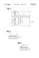
- FIGS. 1 to 3illustrate the initial step of a process of producing an active matrix substrate according to the invention, wherein FIG. 1 is a fragmentary plan view, and FIGS. 2 and 3 are schematic sectional views taken along the line 2--2 and line 3--3 in FIG. 1, respectively;
- FIGS. 4 to 6illustrate the next step of the process, wherein FIG. 4 is a fragmentary plan view, and FIGS, 5 and 6 are schematic sectional views taken along the line 5--5 and line 6--6 in FIG. 4, respectively;
- FIGS. 7 to 9illustrate the last step of the process, wherein FIG. 7 is a fragmentary plan view, and FIGS. 8 and 9 are schematic sectional views taken along the line 8--8 and line 9--9 in FIG. 7, respectively;
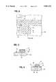
- FIGS. 10 to 12show another active matrix substrate according to the invention, wherein FIG. 10 is a fragmentary plan view, and FIGS. 11 and 12 are schematic sectional views taken along the line 11--11 and line 9--9 in FIG. 10, respectively;
- FIG. 13is a fragmentray plan view of a conventional active matrix substrate
- FIG. 14is a schematic sectional view taken along the line 14--14 in FIG. 13;
- FIG. 15is a fragmentary plan view of another known active matrix substrate
- FIGS. 16 and 17are schematic sectional views taken along the line 16--16 and line 17--17 in FIG. 14, respectively.
- FIGS. 1 to 9illustrate a process of producing an active matrix substrate of a liquid crystal display.
- the structure of the obtained active matrix substratecan be seen in FIGS. 7-9.
- FIGS. 1-3illustrate the initial step.
- a metal filmsuch as a chromium film is deposited by sputtering, and the metal film is patterned by photolithography and subsequent wet or dry etching to form a gate electrode 12, a gate bus line 14 and a drain bus line 16.
- the two bus lines 14 and 16are perpendicular to each other.
- the drain bus line 16is broken in the intersection zone to provide a gap 18 across which the gate bus line 14 extends.
- the gate bus line 14may be broken instead of the drain bus line 16.
- a gate dielectric film 20such as a silicon nitride film is deposited on the substrate 10.
- a semiconductor film 22such as an amorphous silicon film is deposited on the dielectric film 20, and an n-type semiconductor film 24 such as a phosphorus-doped amorphous silicon film on the semiconductor film 22.
- these three films 20, 22, 24are each deposited by a plasma-assisted chemical vapor depostion (CVD) technique.
- the three films 20, 22, 24are patterned together by photolithography and subsequent dry etching to form an island structure over a TFT area containing the gate electrode 12 and over the gate bus line 14 and the gap 18 in the drain bus line 16.
- the drain bus line 16is exposed on both sides of the gate bus line 14.
- a transparent conductor filmsuch as an ITO film is deposited by sputtering, and the deposited film is patterned by photolithography and subsequent dry etching to form a drain electrode 26, a supplementary bus line 28 which is contiguous to the drain electrode 26, a source electrode 30, a pixel electrode 32 which is contiguous to the source electrode 30.
- the supplementary bus line 28extends over the island structure of the films 20, 22, 24 above the gap 18 in the drain bus line 16 and makes direct contact with the drain bus line 16 on both sides of the gap 18. That is, the supplementary bus line 28 bridges the gap 18 and connects the drain bus line 16 to the drain electrode 26 to complete the drain bus line.
- the n-type semiconductor film 24is etched by dry etching in the region between the drain and source electrodes 26 and 30 to provide the channel of the TFT.
- the above described processentails only three photolithography steps, i.e., the first photolithography for forming the gate electrode 12, gate bus line 14 and the broken drain bus line 16, the second for forming the island structure of the dielectric film 20 and semiconductor films 22, 24, and the third for forming the drain electrode 26, supplementary bus line 28, source electrode 30 and pixel electrode 32.
- FIGS. 10-12show another embodiment of the invention.
- the TFTis of the inverted structure, whereas in FIGS. 10-12 the TFT is of the normal structure.
- a silicon oxide film 36is deposited by sputtering or by CVD.
- An ITO film(or another transparent conductor film) is deposited on the silicon oxide film 36 by sputtering, and the ITO film is patterned by photolithography and subsequent wet etching to form a drain electrode 26, a supplementary bus line 28 which is contiguous to the drain electrode 26, a source electrode 30 and a pixel electrode 32 which is contiguous to the source electrode 30.
- the supplementary bus line 28extends in the same direction as the drain bus line (16) to be formed later.
- the silicon oxide film 36is left unpatterned.
- the patterned ITO filmis treated, together with the silicon oxide film 36, with a plasma of phosphine PH 3 .
- the silicon oxide film 36is formed for the purpose of providing selectivity in this phosphine plasma treatment.
- an amorphous silicon film (or another semiconductor film) 22 and a silicon nitride film (or another dielectric film) 20are successively deposited each by plasma-assisted CVD, and the two films 20, 22 are patterned together by photolithography and subsequent dry etching to form an island structure over a TFT area containing the drain and source electrodes 26 and 30 and an elongate area in which the gate bus line is to be formed later. A portion of the drain electrode 26 is left exposed.
- a metal filmsuch as a chromiun film is deposited over the whole area, and the metal film is patterned by photolithography and subsequent wet or dry etching to form a gate electrode 12 and a gate bus line 14 on the island structure of the semiconductor and dielectric films 22, 20 and a drain bus line 16 on the supplementary bus line 28.
- the drain bus line 16is broken to provide a gap 18 across which the gate bus line 14 extends.
- the supplementary bus line 28bridges the gap 18 to complete the drain bus line.
- the fabrication processentails only three photolithography steps.
Landscapes
- Physics & Mathematics (AREA)
- Nonlinear Science (AREA)
- Mathematical Physics (AREA)
- Chemical & Material Sciences (AREA)
- Crystallography & Structural Chemistry (AREA)
- General Physics & Mathematics (AREA)
- Optics & Photonics (AREA)
- Engineering & Computer Science (AREA)
- Microelectronics & Electronic Packaging (AREA)
- Liquid Crystal (AREA)
- Thin Film Transistor (AREA)
Abstract
Description
Claims (12)
Applications Claiming Priority (2)
| Application Number | Priority Date | Filing Date | Title |
|---|---|---|---|
| JP8-074509 | 1996-03-28 | ||
| JP7450996AJPH09265113A (en) | 1996-03-28 | 1996-03-28 | Active matrix type liquid crystal display device and its production |
Publications (1)
| Publication Number | Publication Date |
|---|---|
| US5867233Atrue US5867233A (en) | 1999-02-02 |
Family
ID=13549375
Family Applications (1)
| Application Number | Title | Priority Date | Filing Date |
|---|---|---|---|
| US08/828,743Expired - LifetimeUS5867233A (en) | 1996-03-28 | 1997-03-26 | Active matrix liquid crystal display substrate with island structure covering break in signal bus line and method of producing same |
Country Status (4)
| Country | Link |
|---|---|
| US (1) | US5867233A (en) |
| JP (1) | JPH09265113A (en) |
| KR (1) | KR100270467B1 (en) |
| TW (1) | TW318921B (en) |
Cited By (83)
| Publication number | Priority date | Publication date | Assignee | Title |
|---|---|---|---|---|
| US5966589A (en)* | 1996-12-18 | 1999-10-12 | Nec Corporation | Method of fabricating thin film transistor array |
| US5990998A (en)* | 1996-06-07 | 1999-11-23 | Lg Electronics Inc. | Active matrix liquid crystal display and related method |
| US20020017645A1 (en)* | 2000-05-12 | 2002-02-14 | Semiconductor Energy Laboratory Co., Ltd. | Electro-optical device |
| US6424389B1 (en) | 1995-07-25 | 2002-07-23 | Hitachi, Ltd. | Fabrication method of liquid crystal display device |
| US20020132396A1 (en)* | 2000-03-08 | 2002-09-19 | Semiconductor Energy Laboratory Co., Ltd. | Semiconductor device and manufacturing method thereof |
| US20020135709A1 (en)* | 2001-03-21 | 2002-09-26 | Gee Sung Chae | Liquid crystal display device and fabricating method thereof |
| US20020171085A1 (en)* | 2001-03-06 | 2002-11-21 | Hideomi Suzawa | Semiconductor device and manufacturing method thereof |
| US20030079227A1 (en)* | 1998-07-29 | 2003-04-24 | Starsight Telecast, Inc. | Multiple interactive electronic program guide system and methods |
| US20030132896A1 (en)* | 2001-11-21 | 2003-07-17 | Seiko Epson Corporation | Active matrix substrate, electro-optical device, and electronic device |
| US20030138998A1 (en)* | 2000-03-06 | 2003-07-24 | Semiconductor Energy Laboratory Co., Ltd. | Semiconductor device and method of fabricating the same |
| US20030160236A1 (en)* | 2000-03-13 | 2003-08-28 | Semiconductor Energy Laboratory Co., Ltd. | Semiconductor device and a method of manufacturing the same |
| US6683660B1 (en)* | 2000-05-05 | 2004-01-27 | Chi Mei Optoelectronics Corp. | Active matrix liquid crystal display and method of making the same |
| US20040103439A1 (en)* | 1996-10-16 | 2004-05-27 | Gemstar Development Corporation | Access to internet data through a television system |
| US20040210935A1 (en)* | 1995-10-02 | 2004-10-21 | Starsight Telecast, Inc. | Interactive computer system for providing television schedule information |
| US20050028218A1 (en)* | 1996-09-03 | 2005-02-03 | Starsight Telecast, Inc. | Schedule system with enhanced recording capability |
| US20050028208A1 (en)* | 1998-07-17 | 2005-02-03 | United Video Properties, Inc. | Interactive television program guide with remote access |
| US6855957B1 (en) | 2000-03-13 | 2005-02-15 | Semiconductor Energy Laboratory Co., Ltd. | Semiconductor device and manufacturing method thereof |
| US20050056848A1 (en)* | 2000-01-26 | 2005-03-17 | Semiconductor Energy Laboratory Co., Ltd. A Japan Corporation | Semiconductor device and manufacturing method thereof |
| US6890783B2 (en) | 1999-12-28 | 2005-05-10 | Nec Lcd Technologies, Ltd. | Active matrix substrate plate and manufacturing method therefor |
| US6900084B1 (en) | 2000-05-09 | 2005-05-31 | Semiconductor Energy Laboratory Co., Ltd. | Semiconductor device having a display device |
| US20050138660A1 (en)* | 1997-09-18 | 2005-06-23 | United Video Properties, Inc. | Electronic mail reminder for an internet television program guide |
| US20050147247A1 (en)* | 2003-11-14 | 2005-07-07 | Westberg Thomas E. | Interactive television systems having POD modules and methods for use in the same |
| US20050162602A1 (en)* | 2000-01-26 | 2005-07-28 | Semiconductor Energy Laboratory Co., Ltd. A Japan Corporation | Liquid-crystal display device and method of fabricating the same |
| US20050251827A1 (en)* | 1998-07-17 | 2005-11-10 | United Video Properties, Inc. | Interactive television program guide system having multiple devices within a household |
| US20050278768A1 (en)* | 1996-12-10 | 2005-12-15 | United Video Properties, Inc. | Internet television program guide system |
| US7102718B1 (en)* | 2000-03-16 | 2006-09-05 | Semiconductor Energy Laboratory Co., Ltd. | Liquid crystal display device with particular TFT structure and method of manufacturing the same |
| US20060273317A1 (en)* | 2000-04-27 | 2006-12-07 | Semiconductor Energy Laboratory Co., Ltd. | Semiconductor Device and Method of Fabricating the Same |
| US20070146568A1 (en)* | 2000-03-17 | 2007-06-28 | Semiconductor Energy Laboratory Co., Ltd. | Liquid crystal display device and manufacturing method thereof |
| US20070157247A1 (en)* | 2005-12-29 | 2007-07-05 | United Video Properties, Inc. | Systems and methods for managing content |
| US20070157222A1 (en)* | 2005-12-29 | 2007-07-05 | United Video Properties, Inc. | Systems and methods for managing content |
| US20070245019A1 (en)* | 2006-04-12 | 2007-10-18 | United Video Properties, Inc. | Interactive media content delivery using a backchannel communications network |
| US20080155600A1 (en)* | 2006-12-20 | 2008-06-26 | United Video Properties, Inc. | Systems and methods for providing remote access to interactive media guidance applications |
| US20080155607A1 (en)* | 2006-12-20 | 2008-06-26 | United Video Properties, Inc. | Systems and methods for providing remote access to interactive media guidance applications |
| US20090069038A1 (en)* | 2007-09-07 | 2009-03-12 | United Video Properties, Inc. | Cross-platform messaging |
| US20090072228A1 (en)* | 2007-09-19 | 2009-03-19 | Tae-Young Choi | Organic thin film transistor substrate and method of manufacture |
| US20090165051A1 (en)* | 2007-12-19 | 2009-06-25 | United Video Properties, Inc. | Methods and devices for presenting an interactive media guidance application |
| US20090228912A1 (en)* | 1998-05-15 | 2009-09-10 | United Video Properties, Inc. | Systems and methods for advertising television networks, channels, and programs |
| US20090313658A1 (en)* | 2008-06-13 | 2009-12-17 | United Video Properties, Inc. | Systems and methods for displaying media content and media guidance information |
| US20100153997A1 (en)* | 2004-01-21 | 2010-06-17 | United Video Properties, Inc. | Interactive television system with templates for managing vendor-specific video-on-demand content |
| US20100223640A1 (en)* | 1999-12-10 | 2010-09-02 | United Video Properties, Inc. | Systems and methods for coordinating interactive and passive advertisement and merchandising opportunities |
| US20100262931A1 (en)* | 2009-04-10 | 2010-10-14 | Rovi Technologies Corporation | Systems and methods for searching a media guidance application with multiple perspective views |
| US20100262260A1 (en)* | 2002-08-22 | 2010-10-14 | Victhom Human Bionics, Inc. | Actuated prosthesis for amputess |
| US20100306708A1 (en)* | 2009-05-29 | 2010-12-02 | Rovi Techonologies Corporation | Systems and methods for handling profiles in a community |
| US20100311399A1 (en)* | 2005-03-31 | 2010-12-09 | United Video Properties, Inc. | Systems and methods for generating audible reminders on mobile user equipment |
| US20100310230A1 (en)* | 1998-07-14 | 2010-12-09 | United Video Properties, Inc. | Client-server based interactive television program guide system with remote server recording |
| US20110016492A1 (en)* | 2009-07-16 | 2011-01-20 | Gemstar Development Corporation | Systems and methods for forwarding media asset events |
| US20110070819A1 (en)* | 2009-09-23 | 2011-03-24 | Rovi Technologies Corporation | Systems and methods for providing reminders associated with detected users |
| US20110072452A1 (en)* | 2009-09-23 | 2011-03-24 | Rovi Technologies Corporation | Systems and methods for providing automatic parental control activation when a restricted user is detected within range of a device |
| US20110163939A1 (en)* | 2010-01-05 | 2011-07-07 | Rovi Technologies Corporation | Systems and methods for transferring content between user equipment and a wireless communications device |
| US20110197222A1 (en)* | 2000-02-01 | 2011-08-11 | United Video Properties, Inc. | Systems and methods for providing promotions with recorded programs |
| US20110197232A1 (en)* | 2007-12-19 | 2011-08-11 | United Video Properties, Inc. | Methods and devices for presenting an interactive media guidance application |
| US20110292327A1 (en)* | 2007-02-15 | 2011-12-01 | Au Optronics Corporation | Light reflecting structure in a liquid crystal display panel |
| US8087047B2 (en) | 2007-04-20 | 2011-12-27 | United Video Properties, Inc. | Systems and methods for providing remote access to interactive media guidance applications |
| US8327403B1 (en) | 2007-09-07 | 2012-12-04 | United Video Properties, Inc. | Systems and methods for providing remote program ordering on a user device via a web server |
| US8453174B2 (en) | 1995-10-02 | 2013-05-28 | Starsight Telecast, Inc. | Method and system for displaying advertising, video, and program schedule listing |
| US8761584B2 (en) | 1993-03-05 | 2014-06-24 | Gemstar Development Corporation | System and method for searching a database of television schedule information |
| US8776125B2 (en) | 1996-05-03 | 2014-07-08 | Starsight Telecast Inc. | Method and system for displaying advertisements in an electronic program guide |
| US8806533B1 (en) | 2004-10-08 | 2014-08-12 | United Video Properties, Inc. | System and method for using television information codes |
| US8832742B2 (en) | 2006-10-06 | 2014-09-09 | United Video Properties, Inc. | Systems and methods for acquiring, categorizing and delivering media in interactive media guidance applications |
| US8892495B2 (en) | 1991-12-23 | 2014-11-18 | Blanding Hovenweep, Llc | Adaptive pattern recognition based controller apparatus and method and human-interface therefore |
| US8904441B2 (en) | 2003-11-06 | 2014-12-02 | United Video Properties, Inc. | Systems and methods for providing program suggestions in an interactive television program guide |
| US8949901B2 (en) | 2011-06-29 | 2015-02-03 | Rovi Guides, Inc. | Methods and systems for customizing viewing environment preferences in a viewing environment control application |
| US9014546B2 (en) | 2009-09-23 | 2015-04-21 | Rovi Guides, Inc. | Systems and methods for automatically detecting users within detection regions of media devices |
| US9071872B2 (en) | 2003-01-30 | 2015-06-30 | Rovi Guides, Inc. | Interactive television systems with digital video recording and adjustable reminders |
| US9113207B2 (en) | 1995-10-02 | 2015-08-18 | Rovi Guides, Inc. | Systems and methods for contextually linking television program information |
| US9125169B2 (en) | 2011-12-23 | 2015-09-01 | Rovi Guides, Inc. | Methods and systems for performing actions based on location-based rules |
| US9137491B2 (en) | 2000-02-01 | 2015-09-15 | Rovi Guides, Inc. | Methods and systems for forced advertising |
| US9167196B2 (en) | 2010-05-19 | 2015-10-20 | Rovi Guides, Inc. | Systems and methods for trimming recorded content using a media guidance application |
| US9166714B2 (en) | 2009-09-11 | 2015-10-20 | Veveo, Inc. | Method of and system for presenting enriched video viewing analytics |
| US9191722B2 (en) | 1997-07-21 | 2015-11-17 | Rovi Guides, Inc. | System and method for modifying advertisement responsive to EPG information |
| US9197943B2 (en) | 1998-12-03 | 2015-11-24 | Rovi Guides, Inc. | Electronic program guide with related-program search feature |
| US9204193B2 (en) | 2010-05-14 | 2015-12-01 | Rovi Guides, Inc. | Systems and methods for media detection and filtering using a parental control logging application |
| US9218122B2 (en) | 2011-12-29 | 2015-12-22 | Rovi Guides, Inc. | Systems and methods for transferring settings across devices based on user gestures |
| US9253262B2 (en) | 2013-01-24 | 2016-02-02 | Rovi Guides, Inc. | Systems and methods for connecting media devices through web sockets |
| US9288521B2 (en) | 2014-05-28 | 2016-03-15 | Rovi Guides, Inc. | Systems and methods for updating media asset data based on pause point in the media asset |
| US9294799B2 (en) | 2000-10-11 | 2016-03-22 | Rovi Guides, Inc. | Systems and methods for providing storage of data on servers in an on-demand media delivery system |
| US9307281B2 (en) | 2007-03-22 | 2016-04-05 | Rovi Guides, Inc. | User defined rules for assigning destinations of content |
| US9319735B2 (en) | 1995-06-07 | 2016-04-19 | Rovi Guides, Inc. | Electronic television program guide schedule system and method with data feed access |
| US9326025B2 (en) | 2007-03-09 | 2016-04-26 | Rovi Technologies Corporation | Media content search results ranked by popularity |
| US9426509B2 (en) | 1998-08-21 | 2016-08-23 | Rovi Guides, Inc. | Client-server electronic program guide |
| US9535563B2 (en) | 1999-02-01 | 2017-01-03 | Blanding Hovenweep, Llc | Internet appliance system and method |
| US9674563B2 (en) | 2013-11-04 | 2017-06-06 | Rovi Guides, Inc. | Systems and methods for recommending content |
| US10063934B2 (en) | 2008-11-25 | 2018-08-28 | Rovi Technologies Corporation | Reducing unicast session duration with restart TV |
Families Citing this family (6)
| Publication number | Priority date | Publication date | Assignee | Title |
|---|---|---|---|---|
| KR100348995B1 (en)* | 1999-09-08 | 2002-08-17 | 엘지.필립스 엘시디 주식회사 | The method for fabricating liquid crystal display using four masks and the liquid crystal display thereof |
| EP1220187A4 (en)* | 1999-09-08 | 2005-05-18 | Matsushita Electric Industrial Co Ltd | ELECTRIC CIRCUIT BOARD, TFT MATRIX SUBSTRATE UTILIZING THIS CARD AND LIQUID CRYSTAL DISPLAY |
| JP2001147651A (en)* | 1999-09-08 | 2001-05-29 | Matsushita Electric Ind Co Ltd | Electric circuit substrate, TFT array substrate and liquid crystal display device using the same |
| US6930732B2 (en) | 2000-10-11 | 2005-08-16 | Lg.Philips Lcd Co., Ltd. | Array substrate for a liquid crystal display |
| KR100467176B1 (en)* | 2000-10-11 | 2005-01-24 | 엘지.필립스 엘시디 주식회사 | Array pannel of liquid crystal display and fabricating method the same |
| JP4516518B2 (en) | 2005-03-15 | 2010-08-04 | 株式会社フューチャービジョン | Liquid crystal display device using thin film transistor and manufacturing method thereof |
Citations (7)
| Publication number | Priority date | Publication date | Assignee | Title |
|---|---|---|---|---|
| JPS60128486A (en)* | 1983-12-16 | 1985-07-09 | 株式会社日本自動車部品総合研究所 | Display unit |
| US4738749A (en)* | 1986-01-27 | 1988-04-19 | Francois Maurice | Process for producing an active matrix display screen with gate resistance |
| JPH01282522A (en)* | 1988-05-10 | 1989-11-14 | Hitachi Ltd | Active matrix circuit board, manufacturing method thereof, and image display device using the same |
| US5346833A (en)* | 1993-04-05 | 1994-09-13 | Industrial Technology Research Institute | Simplified method of making active matrix liquid crystal display |
| US5470768A (en)* | 1992-08-07 | 1995-11-28 | Fujitsu Limited | Method for fabricating a thin-film transistor |
| US5668379A (en)* | 1994-07-27 | 1997-09-16 | Hitachi, Ltd. | Active matrix crystal display apparatus using thin film transistor |
| US5694185A (en)* | 1995-11-25 | 1997-12-02 | Lg Electronics Inc. | Matrix array of active matrix LCD and manufacturing method thereof |
Family Cites Families (5)
| Publication number | Priority date | Publication date | Assignee | Title |
|---|---|---|---|---|
| JPS63240527A (en)* | 1987-03-27 | 1988-10-06 | Matsushita Electric Ind Co Ltd | thin film transistor array |
| US5032883A (en)* | 1987-09-09 | 1991-07-16 | Casio Computer Co., Ltd. | Thin film transistor and method of manufacturing the same |
| JPH02170135A (en)* | 1988-12-23 | 1990-06-29 | Nec Corp | Thin-film field effect type transistor element array |
| JP2625585B2 (en)* | 1991-03-08 | 1997-07-02 | 沖電気工業株式会社 | Thin film transistor array substrate and method of manufacturing the same |
| JP2801104B2 (en)* | 1992-01-29 | 1998-09-21 | シャープ株式会社 | Manufacturing method of active matrix drive type scattering type liquid crystal display device |
- 1996
- 1996-03-28JPJP7450996Apatent/JPH09265113A/enactivePending
- 1997
- 1997-03-26USUS08/828,743patent/US5867233A/ennot_activeExpired - Lifetime
- 1997-03-26TWTW086103849Apatent/TW318921B/zhnot_activeIP Right Cessation
- 1997-03-28KRKR1019970012140Apatent/KR100270467B1/ennot_activeExpired - Fee Related
Patent Citations (7)
| Publication number | Priority date | Publication date | Assignee | Title |
|---|---|---|---|---|
| JPS60128486A (en)* | 1983-12-16 | 1985-07-09 | 株式会社日本自動車部品総合研究所 | Display unit |
| US4738749A (en)* | 1986-01-27 | 1988-04-19 | Francois Maurice | Process for producing an active matrix display screen with gate resistance |
| JPH01282522A (en)* | 1988-05-10 | 1989-11-14 | Hitachi Ltd | Active matrix circuit board, manufacturing method thereof, and image display device using the same |
| US5470768A (en)* | 1992-08-07 | 1995-11-28 | Fujitsu Limited | Method for fabricating a thin-film transistor |
| US5346833A (en)* | 1993-04-05 | 1994-09-13 | Industrial Technology Research Institute | Simplified method of making active matrix liquid crystal display |
| US5668379A (en)* | 1994-07-27 | 1997-09-16 | Hitachi, Ltd. | Active matrix crystal display apparatus using thin film transistor |
| US5694185A (en)* | 1995-11-25 | 1997-12-02 | Lg Electronics Inc. | Matrix array of active matrix LCD and manufacturing method thereof |
Cited By (251)
| Publication number | Priority date | Publication date | Assignee | Title |
|---|---|---|---|---|
| US8892495B2 (en) | 1991-12-23 | 2014-11-18 | Blanding Hovenweep, Llc | Adaptive pattern recognition based controller apparatus and method and human-interface therefore |
| US8761584B2 (en) | 1993-03-05 | 2014-06-24 | Gemstar Development Corporation | System and method for searching a database of television schedule information |
| US9319735B2 (en) | 1995-06-07 | 2016-04-19 | Rovi Guides, Inc. | Electronic television program guide schedule system and method with data feed access |
| US20060012727A1 (en)* | 1995-07-25 | 2006-01-19 | Kikuo Ono | Liquid crystal display device and method of making same |
| US7271870B2 (en) | 1995-07-25 | 2007-09-18 | Hitachi, Ltd. | Liquid crystal display device and method of making same |
| US6424389B1 (en) | 1995-07-25 | 2002-07-23 | Hitachi, Ltd. | Fabrication method of liquid crystal display device |
| US6839106B2 (en) | 1995-07-25 | 2005-01-04 | Hitachi, Ltd. | Liquid crystal display device and method of making same |
| US20040046904A1 (en)* | 1995-07-25 | 2004-03-11 | Kikuo Ono | Liquid crystal display device and method of making same |
| US6590623B2 (en) | 1995-07-25 | 2003-07-08 | Hitachi, Ltd. | Fabrication method of liquid crystal display device having a reduced number of process steps |
| US9402102B2 (en) | 1995-10-02 | 2016-07-26 | Rovi Guides, Inc. | System and method for using television schedule information |
| US8205232B2 (en) | 1995-10-02 | 2012-06-19 | Starsight Telecast, Inc. | Interactive computer system for providing television schedule information |
| US20100211969A1 (en)* | 1995-10-02 | 2010-08-19 | Schein Steven M | Interactive computer system for providing television schedule information |
| US20100115541A1 (en)* | 1995-10-02 | 2010-05-06 | Starsight Telecast, Inc. | Interactive Computer System for Providing Television Schedule Information |
| US20080288980A1 (en)* | 1995-10-02 | 2008-11-20 | Starsight Telecast, Inc. | Interactive computer system for providing television schedule information |
| US9124932B2 (en) | 1995-10-02 | 2015-09-01 | Rovi Guides, Inc. | Systems and methods for contextually linking television program information |
| US9918035B2 (en) | 1995-10-02 | 2018-03-13 | Rovi Guides, Inc. | Interactive computer system for providing television schedule information |
| US20110173660A1 (en)* | 1995-10-02 | 2011-07-14 | Starsight Telecast, Inc. | Interactive computer system for providing television schedule information |
| US9113207B2 (en) | 1995-10-02 | 2015-08-18 | Rovi Guides, Inc. | Systems and methods for contextually linking television program information |
| US20100115413A1 (en)* | 1995-10-02 | 2010-05-06 | Starsight Telecast, Inc. | Interactive Computer System For Providing Television Schedule Information |
| US8453174B2 (en) | 1995-10-02 | 2013-05-28 | Starsight Telecast, Inc. | Method and system for displaying advertising, video, and program schedule listing |
| US20040210935A1 (en)* | 1995-10-02 | 2004-10-21 | Starsight Telecast, Inc. | Interactive computer system for providing television schedule information |
| US9667903B2 (en) | 1995-10-02 | 2017-05-30 | Rovi Guides, Inc. | Interactive computer system for providing television schedule information |
| US8776125B2 (en) | 1996-05-03 | 2014-07-08 | Starsight Telecast Inc. | Method and system for displaying advertisements in an electronic program guide |
| US5990998A (en)* | 1996-06-07 | 1999-11-23 | Lg Electronics Inc. | Active matrix liquid crystal display and related method |
| US20050028218A1 (en)* | 1996-09-03 | 2005-02-03 | Starsight Telecast, Inc. | Schedule system with enhanced recording capability |
| US20040103439A1 (en)* | 1996-10-16 | 2004-05-27 | Gemstar Development Corporation | Access to internet data through a television system |
| US9003451B2 (en) | 1996-12-10 | 2015-04-07 | Rovi Guides, Inc. | Internet television program guide system |
| US20080201740A1 (en)* | 1996-12-10 | 2008-08-21 | United Video Properties, Inc. | Internet television program guide system |
| US20080276283A1 (en)* | 1996-12-10 | 2008-11-06 | Boyer Franklin E | Internet television program guide system |
| US20110191808A1 (en)* | 1996-12-10 | 2011-08-04 | United Video Properties, Inc. | Internet television program guide system |
| US20100211975A1 (en)* | 1996-12-10 | 2010-08-19 | Boyer Franklin E | Internet television program guide system |
| US20050278768A1 (en)* | 1996-12-10 | 2005-12-15 | United Video Properties, Inc. | Internet television program guide system |
| US5966589A (en)* | 1996-12-18 | 1999-10-12 | Nec Corporation | Method of fabricating thin film transistor array |
| US9191722B2 (en) | 1997-07-21 | 2015-11-17 | Rovi Guides, Inc. | System and method for modifying advertisement responsive to EPG information |
| US8762492B2 (en) | 1997-09-18 | 2014-06-24 | United Video Properties, Inc. | Electronic mail reminder for an internet television program guide |
| US20050138660A1 (en)* | 1997-09-18 | 2005-06-23 | United Video Properties, Inc. | Electronic mail reminder for an internet television program guide |
| US8352978B2 (en) | 1998-05-15 | 2013-01-08 | United Video Properties, Inc. | Systems and methods for advertising television networks, channels, and programs |
| US20090228912A1 (en)* | 1998-05-15 | 2009-09-10 | United Video Properties, Inc. | Systems and methods for advertising television networks, channels, and programs |
| US9055319B2 (en) | 1998-07-14 | 2015-06-09 | Rovi Guides, Inc. | Interactive guide with recording |
| US20100310230A1 (en)* | 1998-07-14 | 2010-12-09 | United Video Properties, Inc. | Client-server based interactive television program guide system with remote server recording |
| US9154843B2 (en) | 1998-07-14 | 2015-10-06 | Rovi Guides, Inc. | Client-server based interactive guide with server recording |
| US9118948B2 (en) | 1998-07-14 | 2015-08-25 | Rovi Guides, Inc. | Client-server based interactive guide with server recording |
| US9226006B2 (en) | 1998-07-14 | 2015-12-29 | Rovi Guides, Inc. | Client-server based interactive guide with server recording |
| US9232254B2 (en) | 1998-07-14 | 2016-01-05 | Rovi Guides, Inc. | Client-server based interactive television guide with server recording |
| US9055318B2 (en) | 1998-07-14 | 2015-06-09 | Rovi Guides, Inc. | Client-server based interactive guide with server storage |
| US10075746B2 (en) | 1998-07-14 | 2018-09-11 | Rovi Guides, Inc. | Client-server based interactive television guide with server recording |
| US8776126B2 (en) | 1998-07-14 | 2014-07-08 | United Video Properties, Inc. | Client-server based interactive television guide with server recording |
| US8528032B2 (en) | 1998-07-14 | 2013-09-03 | United Video Properties, Inc. | Client-server based interactive television program guide system with remote server recording |
| US9021538B2 (en) | 1998-07-14 | 2015-04-28 | Rovi Guides, Inc. | Client-server based interactive guide with server recording |
| US20080189743A1 (en)* | 1998-07-17 | 2008-08-07 | Ellis Michael D | Interactive television program guide with remote access |
| US20080189742A1 (en)* | 1998-07-17 | 2008-08-07 | Ellis Michael D | Interactive television program guide with remote access |
| US10271088B2 (en) | 1998-07-17 | 2019-04-23 | Rovi Guides, Inc. | Interactive television program guide with remote access |
| US20050251827A1 (en)* | 1998-07-17 | 2005-11-10 | United Video Properties, Inc. | Interactive television program guide system having multiple devices within a household |
| US20060031883A1 (en)* | 1998-07-17 | 2006-02-09 | United Video Properties, Inc. | Interactive television program guide with remote access |
| US20050028208A1 (en)* | 1998-07-17 | 2005-02-03 | United Video Properties, Inc. | Interactive television program guide with remote access |
| US9706245B2 (en) | 1998-07-17 | 2017-07-11 | Rovi Guides, Inc. | Interactive television program guide system having multiple devices within a household |
| US8006263B2 (en) | 1998-07-17 | 2011-08-23 | United Video Properties, Inc. | Interactive television program guide with remote access |
| US20080010655A1 (en)* | 1998-07-17 | 2008-01-10 | Ellis Michael D | Interactive television program guide with remote access |
| US8768148B2 (en) | 1998-07-17 | 2014-07-01 | United Video Properties, Inc. | Interactive television program guide with remote access |
| US8046801B2 (en) | 1998-07-17 | 2011-10-25 | United Video Properties, Inc. | Interactive television program guide with remote access |
| US20090044226A1 (en)* | 1998-07-17 | 2009-02-12 | Ellis Michael D | Interactive Television Program Guide System Having Multiple Devices Within A Household |
| US9237369B2 (en) | 1998-07-17 | 2016-01-12 | Rovi Guides, Inc. | Interactive television program guide system having multiple devices within a household |
| US9084006B2 (en) | 1998-07-17 | 2015-07-14 | Rovi Guides, Inc. | Interactive television program guide system having multiple devices within a household |
| US20100251303A1 (en)* | 1998-07-17 | 2010-09-30 | United Video Properties, Inc. | Interactive television program guide system having multiple devices within a household |
| US8755666B2 (en) | 1998-07-17 | 2014-06-17 | United Video Properties, Inc. | Interactive television program guide with remote access |
| US9204184B2 (en) | 1998-07-17 | 2015-12-01 | Rovi Guides, Inc. | Interactive television program guide with remote access |
| US7913278B2 (en) | 1998-07-17 | 2011-03-22 | United Video Properties, Inc. | Interactive television program guide with remote access |
| US9185449B2 (en) | 1998-07-17 | 2015-11-10 | Rovi Guides, Inc. | Interactive television program guide system having multiple devices within a household |
| US8578413B2 (en) | 1998-07-17 | 2013-11-05 | United Video Properties, Inc. | Interactive television program guide with remote access |
| US8578423B2 (en) | 1998-07-17 | 2013-11-05 | United Video Properties, Inc. | Interactive television program guide with remote access |
| US8584172B2 (en) | 1998-07-17 | 2013-11-12 | United Video Properties, Inc. | Interactive television program guide with remote access |
| US8566871B2 (en) | 1998-07-29 | 2013-10-22 | Starsight Telecast, Inc. | Multiple interactive electronic program guide system and methods |
| US20030079227A1 (en)* | 1998-07-29 | 2003-04-24 | Starsight Telecast, Inc. | Multiple interactive electronic program guide system and methods |
| US20050251822A1 (en)* | 1998-07-29 | 2005-11-10 | Knowles James H | Multiple interactive electronic program guide system and methods |
| US9426509B2 (en) | 1998-08-21 | 2016-08-23 | Rovi Guides, Inc. | Client-server electronic program guide |
| US9197943B2 (en) | 1998-12-03 | 2015-11-24 | Rovi Guides, Inc. | Electronic program guide with related-program search feature |
| US9535563B2 (en) | 1999-02-01 | 2017-01-03 | Blanding Hovenweep, Llc | Internet appliance system and method |
| US9118958B2 (en) | 1999-12-10 | 2015-08-25 | Rovi Guides, Inc. | Systems and methods for coordinating interactive and passive advertisement and merchandising opportunities |
| US20100223640A1 (en)* | 1999-12-10 | 2010-09-02 | United Video Properties, Inc. | Systems and methods for coordinating interactive and passive advertisement and merchandising opportunities |
| US6890783B2 (en) | 1999-12-28 | 2005-05-10 | Nec Lcd Technologies, Ltd. | Active matrix substrate plate and manufacturing method therefor |
| US8513666B2 (en) | 2000-01-26 | 2013-08-20 | Semiconductor Energy Laboratory Co., Ltd. | Semiconductor device and manufacturing method thereof |
| US20070184665A1 (en)* | 2000-01-26 | 2007-08-09 | Semiconductor Energy Laboratory Co., Ltd. | Semiconductor device and manufacturing method thereof |
| US7567328B2 (en) | 2000-01-26 | 2009-07-28 | Semiconductor Energy Laboratory Co., Ltd. | Liquid-crystal display device and method of fabricating the same |
| US8017456B2 (en) | 2000-01-26 | 2011-09-13 | Semiconductor Energy Laboratory Co., Ltd. | Semiconductor device and manufacturing method thereof |
| US20050162602A1 (en)* | 2000-01-26 | 2005-07-28 | Semiconductor Energy Laboratory Co., Ltd. A Japan Corporation | Liquid-crystal display device and method of fabricating the same |
| US20050056848A1 (en)* | 2000-01-26 | 2005-03-17 | Semiconductor Energy Laboratory Co., Ltd. A Japan Corporation | Semiconductor device and manufacturing method thereof |
| US7799590B2 (en) | 2000-01-26 | 2010-09-21 | Semiconductor Energy Laboratory Co., Ltd. | Semiconductor device and manufacturing method thereof |
| US9137491B2 (en) | 2000-02-01 | 2015-09-15 | Rovi Guides, Inc. | Methods and systems for forced advertising |
| US20110197222A1 (en)* | 2000-02-01 | 2011-08-11 | United Video Properties, Inc. | Systems and methods for providing promotions with recorded programs |
| US20050023528A1 (en)* | 2000-03-06 | 2005-02-03 | Semiconductor Energy | Semiconductor device and method for fabricating the same |
| US7705354B2 (en) | 2000-03-06 | 2010-04-27 | Semiconductor Energy Laboratory Co., Ltd | Semiconductor device and method for fabricating the same |
| US7973312B2 (en) | 2000-03-06 | 2011-07-05 | Semiconductor Energy Laboratory Co., Ltd. | Semiconductor device and method of fabricating the same |
| US6806495B1 (en) | 2000-03-06 | 2004-10-19 | Semiconductor Energy Laboratory Co., Ltd. | Semiconductor device and method of fabricating the same |
| US20100171895A1 (en)* | 2000-03-06 | 2010-07-08 | Semiconductor Energy Laboratory Co., Ltd. | Semiconductor device and method of fabricating the same |
| US9099355B2 (en) | 2000-03-06 | 2015-08-04 | Semiconductor Energy Laboratory Co., Ltd. | Semiconductor device and method of fabricating the same |
| US6762082B2 (en) | 2000-03-06 | 2004-07-13 | Semiconductor Energy Laboratory Co., Ltd. | Semiconductor device and method of fabricating the same |
| US8188478B2 (en) | 2000-03-06 | 2012-05-29 | Semiconductor Energy Laboratory Co., Ltd. | Semiconductor device and method of fabricating the same |
| US20030138998A1 (en)* | 2000-03-06 | 2003-07-24 | Semiconductor Energy Laboratory Co., Ltd. | Semiconductor device and method of fabricating the same |
| US20100238393A1 (en)* | 2000-03-08 | 2010-09-23 | Semiconductor Energy Laboratory Co., Ltd. | Semiconductor device and manufacturing method thereof |
| US7652294B2 (en) | 2000-03-08 | 2010-01-26 | Semiconductor Energy Laboratory Co., Ltd. | Semiconductor device and manufacturing method thereof |
| US7414266B2 (en) | 2000-03-08 | 2008-08-19 | Semiconductor Energy Laboratory Co., Ltd. | Semiconductor device and manufacturing method thereof |
| US9368514B2 (en) | 2000-03-08 | 2016-06-14 | Semiconductor Energy Laboratory Co., Ltd. | Semiconductor device and manufacturing method thereof |
| US20060163574A1 (en)* | 2000-03-08 | 2006-07-27 | Semiconductor Energy Laboratory Co., Ltd. | Semiconductor device and manufacturing method thereof |
| US8198630B2 (en) | 2000-03-08 | 2012-06-12 | Semiconductor Energy Laboratory Co., Ltd. | Semiconductor device and manufacturing method thereof |
| US7019329B2 (en) | 2000-03-08 | 2006-03-28 | Semiconductor Energy Laboratory Co., Ltd. | Semiconductor device and manufacturing method thereof |
| US6747288B2 (en) | 2000-03-08 | 2004-06-08 | Semiconductor Energy Laboratory Co., Ltd. | Semiconductor device and manufacturing method thereof |
| US20090026464A1 (en)* | 2000-03-08 | 2009-01-29 | Semiconductor Energy Laboratory Co., Ltd. | Semiconductor device and manufacturing method thereof |
| US20080315208A1 (en)* | 2000-03-08 | 2008-12-25 | Semiconductor Energy Laboratory Co., Ltd. | Semiconductor device and manufacturing method thereof |
| US8586988B2 (en) | 2000-03-08 | 2013-11-19 | Semiconductor Energy Laboratory Co., Ltd. | Semiconductor device and manufacturing method thereof |
| US9059045B2 (en) | 2000-03-08 | 2015-06-16 | Semiconductor Energy Laboratory Co., Ltd. | Semiconductor device and manufacturing method thereof |
| US9786687B2 (en) | 2000-03-08 | 2017-10-10 | Semiconductor Energy Laboratory Co., Ltd. | Semiconductor device and manufacturing method thereof |
| US20020132396A1 (en)* | 2000-03-08 | 2002-09-19 | Semiconductor Energy Laboratory Co., Ltd. | Semiconductor device and manufacturing method thereof |
| US7728334B2 (en) | 2000-03-08 | 2010-06-01 | Semiconductor Energy Laboratory Co., Ltd. | Semiconductor device and manufacturing method thereof |
| US6709901B1 (en) | 2000-03-13 | 2004-03-23 | Semiconductor Energy Laboratory Co., Ltd. | Semiconductor device having stick drivers and a method of manufacturing the same |
| US7995183B2 (en) | 2000-03-13 | 2011-08-09 | Semiconductor Energy Laboratory Co., Ltd. | Semiconductor device and a method of manufacturing the same |
| US6806499B2 (en) | 2000-03-13 | 2004-10-19 | Semiconductor Energy Laboratory Co., Ltd. | Semiconductor device and a method of manufacturing the same |
| US20030160236A1 (en)* | 2000-03-13 | 2003-08-28 | Semiconductor Energy Laboratory Co., Ltd. | Semiconductor device and a method of manufacturing the same |
| US7687325B2 (en) | 2000-03-13 | 2010-03-30 | Semiconductor Energy Laboratory Co., Ltd. | Semiconductor device and manufacturing method thereof |
| US20050041166A1 (en)* | 2000-03-13 | 2005-02-24 | Semiconductor Energy Laboratory Co., Ltd. | Semiconductor device and a method of manufacturing the same |
| US8300201B2 (en) | 2000-03-13 | 2012-10-30 | Semiconductor Energy Laboratory Co., Ltd. | Semiconductor device and a method of manufacturing the same |
| US8934066B2 (en) | 2000-03-13 | 2015-01-13 | Semiconductor Energy Laboratory Co., Ltd. | Semiconductor device having stick drivers and a method of manufacturing the same |
| US20050221542A1 (en)* | 2000-03-13 | 2005-10-06 | Semiconductor Energy Laboratory Co., Ltd | Semiconductor device and manufacturing method thereof |
| US6855957B1 (en) | 2000-03-13 | 2005-02-15 | Semiconductor Energy Laboratory Co., Ltd. | Semiconductor device and manufacturing method thereof |
| US20070058121A1 (en)* | 2000-03-16 | 2007-03-15 | Semiconductor Energy Laboratory Co., Ltd. | Liquid crystal display device and method of manufacturing the same |
| US7990508B2 (en) | 2000-03-16 | 2011-08-02 | Semiconductor Energy Laboratory Co., Ltd. | Liquid crystal display device and method of manufacturing the same |
| US8873011B2 (en) | 2000-03-16 | 2014-10-28 | Semiconductor Energy Laboratory Co., Ltd. | Liquid crystal display device and method of manufacturing the same |
| US7102718B1 (en)* | 2000-03-16 | 2006-09-05 | Semiconductor Energy Laboratory Co., Ltd. | Liquid crystal display device with particular TFT structure and method of manufacturing the same |
| US8610861B2 (en) | 2000-03-16 | 2013-12-17 | Semiconductor Energy Laboratory Co., Ltd. | Liquid crystal display device and method of manufacturing the same |
| US9298056B2 (en) | 2000-03-16 | 2016-03-29 | Semiconductor Energy Laboratory Co., Ltd. | Liquid crystal display device and method of manufacturing the same |
| US8228477B2 (en) | 2000-03-16 | 2012-07-24 | Semiconductor Energy Laboratory Co., Ltd. | Liquid crystal display device and method of manufacturing the same |
| US7656491B2 (en) | 2000-03-16 | 2010-02-02 | Semiconductor Energy Laboratory Co., Ltd. | Liquid crystal display device and method of manufacturing the same |
| US7714975B1 (en) | 2000-03-17 | 2010-05-11 | Semiconductor Energy Laboratory Co., Ltd | Liquid crystal display device and manfacturing method thereof |
| US8421985B2 (en) | 2000-03-17 | 2013-04-16 | Semiconductor Energy Laboratory Co., Ltd. | Liquid crystal display device and manufacturing method thereof |
| US8558983B2 (en) | 2000-03-17 | 2013-10-15 | Semiconductor Energy Laboratory Co., Ltd. | Liquid crystal display device and manufacturing method thereof |
| US20100195013A1 (en)* | 2000-03-17 | 2010-08-05 | Semiconductor Energy Laboratory Co., Ltd. | Liquid crystal display device and manufacturing method thereof |
| US20070146568A1 (en)* | 2000-03-17 | 2007-06-28 | Semiconductor Energy Laboratory Co., Ltd. | Liquid crystal display device and manufacturing method thereof |
| US20090250704A1 (en)* | 2000-04-27 | 2009-10-08 | Semiconductor Energy Laboratory Co., Ltd. | Semiconductor Device and Method of Fabricating the Same |
| US7781770B2 (en) | 2000-04-27 | 2010-08-24 | Semiconductor Energy Laboratory Co., Ltd. | Semiconductor device and method of fabricating the same |
| US8633488B2 (en) | 2000-04-27 | 2014-01-21 | Semiconductor Energy Laboratory Co., Ltd. | Semiconductor device and method of fabricating the same |
| US8178880B2 (en) | 2000-04-27 | 2012-05-15 | Semiconductor Energy Laboratory Co., Ltd. | Semiconductor device and method of fabricating the same |
| US9780124B2 (en) | 2000-04-27 | 2017-10-03 | Semiconductor Energy Laboratory Co., Ltd. | Display device including pixel comprising first transistor second transistor and light-emitting element |
| US9419026B2 (en) | 2000-04-27 | 2016-08-16 | Semiconductor Energy Laboratory Co., Ltd. | Semiconductor device and method of fabricating the same |
| US20100276696A1 (en)* | 2000-04-27 | 2010-11-04 | Semiconductor Energy Laboratory Co., Ltd. | Semiconductor Device and Method of Fabricating the Same |
| US9099361B2 (en) | 2000-04-27 | 2015-08-04 | Semiconductor Energy Laboratory Co., Ltd. | Semiconductor device and method of fabricating the same |
| US20060273317A1 (en)* | 2000-04-27 | 2006-12-07 | Semiconductor Energy Laboratory Co., Ltd. | Semiconductor Device and Method of Fabricating the Same |
| US7560732B2 (en) | 2000-04-27 | 2009-07-14 | Semiconductor Energy Laboratory Co., Ltd. | Semiconductor device and method of fabricating the same |
| US6683660B1 (en)* | 2000-05-05 | 2004-01-27 | Chi Mei Optoelectronics Corp. | Active matrix liquid crystal display and method of making the same |
| US7323715B2 (en) | 2000-05-09 | 2008-01-29 | Semiconductor Energy Laboratory Co., Ltd. | Semiconductor device and manufacturing method thereof |
| US9429807B2 (en) | 2000-05-09 | 2016-08-30 | Semiconductor Energy Laboratory Co., Ltd. | Semiconductor device and manufacturing method thereof |
| US9048146B2 (en) | 2000-05-09 | 2015-06-02 | Semiconductor Energy Laboratory Co., Ltd. | Semiconductor device and manufacturing method thereof |
| US6900084B1 (en) | 2000-05-09 | 2005-05-31 | Semiconductor Energy Laboratory Co., Ltd. | Semiconductor device having a display device |
| US7102165B2 (en) | 2000-05-09 | 2006-09-05 | Semiconductor Energy Laboratory Co., Ltd. | Semiconductor device and manufacturing method thereof |
| US8525173B2 (en) | 2000-05-09 | 2013-09-03 | Semiconductor Energy Laboratory Co., Ltd. | Semiconductor device and manufacturing method thereof |
| US8823004B2 (en) | 2000-05-09 | 2014-09-02 | Semiconductor Energy Laboratory Co., Ltd. | Semiconductor device and manufacturing method thereof |
| US20070001171A1 (en)* | 2000-05-09 | 2007-01-04 | Semiconductor Energy Laboratory Co., Ltd. | Semiconductor device and manufacturing method thereof |
| US7902550B2 (en) | 2000-05-09 | 2011-03-08 | Semiconductor Energy Laboratory Co., Ltd. | Semiconductor device and manufacturing method thereof |
| US20050205870A1 (en)* | 2000-05-09 | 2005-09-22 | Semiconductor Energy Laboratory Co., Ltd. | Semiconductor device and manufacturing method thereof |
| US7804552B2 (en) | 2000-05-12 | 2010-09-28 | Semiconductor Energy Laboratory Co., Ltd. | Electro-optical device with light shielding portion comprising laminated colored layers, electrical equipment having the same, portable telephone having the same |
| US20020017645A1 (en)* | 2000-05-12 | 2002-02-14 | Semiconductor Energy Laboratory Co., Ltd. | Electro-optical device |
| US9294799B2 (en) | 2000-10-11 | 2016-03-22 | Rovi Guides, Inc. | Systems and methods for providing storage of data on servers in an on-demand media delivery system |
| US7071037B2 (en) | 2001-03-06 | 2006-07-04 | Semiconductor Energy Laboratory Co., Ltd. | Semiconductor device and manufacturing method thereof |
| US20090050888A1 (en)* | 2001-03-06 | 2009-02-26 | Semiconductor Energy Laboratory Co., Ltd. | Semiconductor device and manufacturing method thereof |
| US20110114959A1 (en)* | 2001-03-06 | 2011-05-19 | Semiconductor Energy Laboratory Co., Ltd. | Semiconductor device and manufacturing method thereof |
| US7714329B2 (en) | 2001-03-06 | 2010-05-11 | Semiconductor Energy Laboratory Co., Ltd. | Semiconductor device having thin film transistor |
| US20020171085A1 (en)* | 2001-03-06 | 2002-11-21 | Hideomi Suzawa | Semiconductor device and manufacturing method thereof |
| US8053781B2 (en) | 2001-03-06 | 2011-11-08 | Semiconductor Energy Laboratory Co., Ltd. | Semiconductor device having thin film transistor |
| US20060086935A1 (en)* | 2001-03-06 | 2006-04-27 | Semiconductor Energy Laboratory Co., Ltd. | Semiconductor device and manufacturing method thereof |
| US7420209B2 (en) | 2001-03-06 | 2008-09-02 | Semiconductor Energy Laboratory Co., Ltd. | Semiconductor device |
| US8461596B2 (en) | 2001-03-06 | 2013-06-11 | Semiconductor Energy Laboratory Co., Ltd. | Semiconductor device including semiconductor film with outer end having tapered shape |
| US7875886B2 (en) | 2001-03-06 | 2011-01-25 | Semiconductor Energy Laboratory Co., Ltd. | Semiconductor device having a thin film transistor |
| US20020135709A1 (en)* | 2001-03-21 | 2002-09-26 | Gee Sung Chae | Liquid crystal display device and fabricating method thereof |
| US7492418B2 (en)* | 2001-03-21 | 2009-02-17 | Lg Display Co., Ltd. | Liquid crystal display device with particular metal layer configuration of TFT and fabricating method thereof |
| US20030132896A1 (en)* | 2001-11-21 | 2003-07-17 | Seiko Epson Corporation | Active matrix substrate, electro-optical device, and electronic device |
| EP1447786A4 (en)* | 2001-11-21 | 2008-04-02 | Seiko Epson Corp | ACTIVE MATRIX SUBSTRATE, ELECTRO-OPTICAL APPARATUS AND ELECTRONIC APPARATUS |
| US8525760B2 (en) | 2001-11-21 | 2013-09-03 | Seiko Epson Corporation | Active matrix substrate, electro-optical device, and electronic device |
| US20060267887A1 (en)* | 2001-11-21 | 2006-11-30 | Seiko Epson Corporation | Active matrix substrate, electro-optical device, and electronic device |
| US20060250333A1 (en)* | 2001-11-21 | 2006-11-09 | Seiko Epson Corporation | Active matrix substrate, electro-optical device, and electronic device |
| US7982692B2 (en) | 2001-11-21 | 2011-07-19 | Seiko Epson Corporation | Active matrix substrate, electro-optical device, and electronic device |
| US7483001B2 (en) | 2001-11-21 | 2009-01-27 | Seiko Epson Corporation | Active matrix substrate, electro-optical device, and electronic device |
| US8294637B2 (en) | 2001-11-21 | 2012-10-23 | Seiko Epson Corporation | Active matrix substrate, electro-optical device, and electronic device |
| US20100262260A1 (en)* | 2002-08-22 | 2010-10-14 | Victhom Human Bionics, Inc. | Actuated prosthesis for amputess |
| US9369741B2 (en) | 2003-01-30 | 2016-06-14 | Rovi Guides, Inc. | Interactive television systems with digital video recording and adjustable reminders |
| US9071872B2 (en) | 2003-01-30 | 2015-06-30 | Rovi Guides, Inc. | Interactive television systems with digital video recording and adjustable reminders |
| US8904441B2 (en) | 2003-11-06 | 2014-12-02 | United Video Properties, Inc. | Systems and methods for providing program suggestions in an interactive television program guide |
| US10880607B2 (en) | 2003-11-06 | 2020-12-29 | Rovi Guides, Inc. | Systems and methods for providing program suggestions in an interactive television program guide |
| US10986407B2 (en) | 2003-11-06 | 2021-04-20 | Rovi Guides, Inc. | Systems and methods for providing program suggestions in an interactive television program guide |
| US9191719B2 (en) | 2003-11-06 | 2015-11-17 | Rovi Guides, Inc. | Systems and methods for providing program suggestions in an interactive television program guide |
| US20110083141A1 (en)* | 2003-11-14 | 2011-04-07 | Rovi Technologies Corporation | Interactive television systems having pod modules and methods for use in the same |
| US20050147247A1 (en)* | 2003-11-14 | 2005-07-07 | Westberg Thomas E. | Interactive television systems having POD modules and methods for use in the same |
| US20100153997A1 (en)* | 2004-01-21 | 2010-06-17 | United Video Properties, Inc. | Interactive television system with templates for managing vendor-specific video-on-demand content |
| US8806533B1 (en) | 2004-10-08 | 2014-08-12 | United Video Properties, Inc. | System and method for using television information codes |
| US20100311399A1 (en)* | 2005-03-31 | 2010-12-09 | United Video Properties, Inc. | Systems and methods for generating audible reminders on mobile user equipment |
| US20070157222A1 (en)* | 2005-12-29 | 2007-07-05 | United Video Properties, Inc. | Systems and methods for managing content |
| US20070157247A1 (en)* | 2005-12-29 | 2007-07-05 | United Video Properties, Inc. | Systems and methods for managing content |
| US20070245019A1 (en)* | 2006-04-12 | 2007-10-18 | United Video Properties, Inc. | Interactive media content delivery using a backchannel communications network |
| US8832742B2 (en) | 2006-10-06 | 2014-09-09 | United Video Properties, Inc. | Systems and methods for acquiring, categorizing and delivering media in interactive media guidance applications |
| US20110202958A1 (en)* | 2006-12-20 | 2011-08-18 | United Video Properties, Inc. | Systems and methods for providing remote access to interactive media guidance applications |
| US20100333138A1 (en)* | 2006-12-20 | 2010-12-30 | United Video Properties | Systems and methods for providing remote access to interactive media guidance applications |
| US9197936B2 (en) | 2006-12-20 | 2015-11-24 | Rovi Guides, Inc. | Systems and methods for providing remote access to interactive media guidance applications |
| US8887184B2 (en) | 2006-12-20 | 2014-11-11 | United Video Properties, Inc. | Systems and methods for providing remote access to interactive media guidance applications |
| US20080155607A1 (en)* | 2006-12-20 | 2008-06-26 | United Video Properties, Inc. | Systems and methods for providing remote access to interactive media guidance applications |
| US8209424B2 (en) | 2006-12-20 | 2012-06-26 | United Video Properties, Inc. | Systems and methods for providing remote access to interactive media guidance applications |
| US20080155600A1 (en)* | 2006-12-20 | 2008-06-26 | United Video Properties, Inc. | Systems and methods for providing remote access to interactive media guidance applications |
| US20110292327A1 (en)* | 2007-02-15 | 2011-12-01 | Au Optronics Corporation | Light reflecting structure in a liquid crystal display panel |
| US8488086B2 (en)* | 2007-02-15 | 2013-07-16 | Au Optronics Corporation | Light reflecting structure in a liquid crystal display panel |
| US10694256B2 (en) | 2007-03-09 | 2020-06-23 | Rovi Technologies Corporation | Media content search results ranked by popularity |
| US9326025B2 (en) | 2007-03-09 | 2016-04-26 | Rovi Technologies Corporation | Media content search results ranked by popularity |
| US9307281B2 (en) | 2007-03-22 | 2016-04-05 | Rovi Guides, Inc. | User defined rules for assigning destinations of content |
| US10034054B2 (en) | 2007-04-20 | 2018-07-24 | Rovi Guides, Inc. | Systems and methods for providing remote access to interactive media guidance applications |
| US8087047B2 (en) | 2007-04-20 | 2011-12-27 | United Video Properties, Inc. | Systems and methods for providing remote access to interactive media guidance applications |
| US8959547B2 (en) | 2007-04-20 | 2015-02-17 | Rovi Guides, Inc. | Systems and methods for providing remote access to interactive media guidance applications |
| US8107977B2 (en) | 2007-09-07 | 2012-01-31 | United Video Properties, Inc. | Cross-platform messaging |
| US9456252B2 (en) | 2007-09-07 | 2016-09-27 | Rovi Guides, Inc. | Cross-platform messaging |
| US20090069038A1 (en)* | 2007-09-07 | 2009-03-12 | United Video Properties, Inc. | Cross-platform messaging |
| US9838747B2 (en) | 2007-09-07 | 2017-12-05 | Rovi Guides, Inc. | Cross-platform messaging |
| US8327403B1 (en) | 2007-09-07 | 2012-12-04 | United Video Properties, Inc. | Systems and methods for providing remote program ordering on a user device via a web server |
| US8565797B2 (en) | 2007-09-07 | 2013-10-22 | United Video Properties, Inc. | Cross-platform messaging |
| US20090072228A1 (en)* | 2007-09-19 | 2009-03-19 | Tae-Young Choi | Organic thin film transistor substrate and method of manufacture |
| US8013326B2 (en)* | 2007-09-19 | 2011-09-06 | Samsung Electronics Co., Ltd. | Organic thin film transistor substrate and method of manufacture |
| US20090165051A1 (en)* | 2007-12-19 | 2009-06-25 | United Video Properties, Inc. | Methods and devices for presenting an interactive media guidance application |
| US20110197232A1 (en)* | 2007-12-19 | 2011-08-11 | United Video Properties, Inc. | Methods and devices for presenting an interactive media guidance application |
| US9071372B2 (en) | 2007-12-19 | 2015-06-30 | Rovi Guides, Inc. | Methods and devices for presenting an interactive media guidance application |
| US8978088B2 (en) | 2008-06-13 | 2015-03-10 | Rovi Guides, Inc. | Systems and methods for displaying media content and media guidance information |
| US20090313658A1 (en)* | 2008-06-13 | 2009-12-17 | United Video Properties, Inc. | Systems and methods for displaying media content and media guidance information |
| US8601526B2 (en) | 2008-06-13 | 2013-12-03 | United Video Properties, Inc. | Systems and methods for displaying media content and media guidance information |
| US9414120B2 (en) | 2008-06-13 | 2016-08-09 | Rovi Guides, Inc. | Systems and methods for displaying media content and media guidance information |
| US10063934B2 (en) | 2008-11-25 | 2018-08-28 | Rovi Technologies Corporation | Reducing unicast session duration with restart TV |
| USRE50355E1 (en) | 2008-11-25 | 2025-03-25 | Adeia Technologies Inc. | Reducing unicast session duration with restart TV |
| US20100262938A1 (en)* | 2009-04-10 | 2010-10-14 | Rovi Technologies Corporation | Systems and methods for generating a media guidance application with multiple perspective views |
| US8555315B2 (en) | 2009-04-10 | 2013-10-08 | United Video Properties, Inc. | Systems and methods for navigating a media guidance application with multiple perspective views |
| US20100262995A1 (en)* | 2009-04-10 | 2010-10-14 | Rovi Technologies Corporation | Systems and methods for navigating a media guidance application with multiple perspective views |
| US20100262931A1 (en)* | 2009-04-10 | 2010-10-14 | Rovi Technologies Corporation | Systems and methods for searching a media guidance application with multiple perspective views |
| US8117564B2 (en) | 2009-04-10 | 2012-02-14 | United Video Properties, Inc. | Systems and methods for generating a media guidance application with multiple perspective views |
| US20100306708A1 (en)* | 2009-05-29 | 2010-12-02 | Rovi Techonologies Corporation | Systems and methods for handling profiles in a community |
| US20110016492A1 (en)* | 2009-07-16 | 2011-01-20 | Gemstar Development Corporation | Systems and methods for forwarding media asset events |
| US9166714B2 (en) | 2009-09-11 | 2015-10-20 | Veveo, Inc. | Method of and system for presenting enriched video viewing analytics |
| US20110072452A1 (en)* | 2009-09-23 | 2011-03-24 | Rovi Technologies Corporation | Systems and methods for providing automatic parental control activation when a restricted user is detected within range of a device |
| US10631066B2 (en) | 2009-09-23 | 2020-04-21 | Rovi Guides, Inc. | Systems and method for automatically detecting users within detection regions of media devices |
| US20110070819A1 (en)* | 2009-09-23 | 2011-03-24 | Rovi Technologies Corporation | Systems and methods for providing reminders associated with detected users |
| US10085072B2 (en) | 2009-09-23 | 2018-09-25 | Rovi Guides, Inc. | Systems and methods for automatically detecting users within detection regions of media devices |
| US9014546B2 (en) | 2009-09-23 | 2015-04-21 | Rovi Guides, Inc. | Systems and methods for automatically detecting users within detection regions of media devices |
| US9201627B2 (en) | 2010-01-05 | 2015-12-01 | Rovi Guides, Inc. | Systems and methods for transferring content between user equipment and a wireless communications device |
| US20110163939A1 (en)* | 2010-01-05 | 2011-07-07 | Rovi Technologies Corporation | Systems and methods for transferring content between user equipment and a wireless communications device |
| US9204193B2 (en) | 2010-05-14 | 2015-12-01 | Rovi Guides, Inc. | Systems and methods for media detection and filtering using a parental control logging application |
| US9167196B2 (en) | 2010-05-19 | 2015-10-20 | Rovi Guides, Inc. | Systems and methods for trimming recorded content using a media guidance application |
| US8949901B2 (en) | 2011-06-29 | 2015-02-03 | Rovi Guides, Inc. | Methods and systems for customizing viewing environment preferences in a viewing environment control application |
| US9125169B2 (en) | 2011-12-23 | 2015-09-01 | Rovi Guides, Inc. | Methods and systems for performing actions based on location-based rules |
| US9218122B2 (en) | 2011-12-29 | 2015-12-22 | Rovi Guides, Inc. | Systems and methods for transferring settings across devices based on user gestures |
| US9253262B2 (en) | 2013-01-24 | 2016-02-02 | Rovi Guides, Inc. | Systems and methods for connecting media devices through web sockets |
| US9674563B2 (en) | 2013-11-04 | 2017-06-06 | Rovi Guides, Inc. | Systems and methods for recommending content |
| US9288521B2 (en) | 2014-05-28 | 2016-03-15 | Rovi Guides, Inc. | Systems and methods for updating media asset data based on pause point in the media asset |
Also Published As
| Publication number | Publication date |
|---|---|
| KR970066697A (en) | 1997-10-13 |
| TW318921B (en) | 1997-11-01 |
| KR100270467B1 (en) | 2000-11-01 |
| JPH09265113A (en) | 1997-10-07 |
Similar Documents
| Publication | Publication Date | Title |
|---|---|---|
| US5867233A (en) | Active matrix liquid crystal display substrate with island structure covering break in signal bus line and method of producing same | |
| US5828433A (en) | Liquid crystal display device and a method of manufacturing the same | |
| US7632723B2 (en) | Thin film transistor array panel and manufacturing method thereof | |
| JP2738289B2 (en) | Manufacturing method of liquid crystal display device | |
| US20030122127A1 (en) | Thin film transistor array and its manufacturing method | |
| JPH07104312A (en) | Production of liquid crystal display device | |
| KR100264757B1 (en) | Active matrix lcd and method of producing the same | |
| US5995174A (en) | Liquid crystal display apparatus with source/drain electrodes and pixel electrode formed by the same material | |
| US4990460A (en) | Fabrication method for thin film field effect transistor array suitable for liquid crystal display | |
| US7599037B2 (en) | Thin film transistor array panel for liquid crystal display and method for manufacturing the same | |
| JPH0720489A (en) | Matrix display | |
| US6862051B2 (en) | Liquid crystal display device and method of manufacturing the same | |
| JPH1048664A (en) | Liquid crystal display device and its production | |
| JPS61187272A (en) | Thin-film field-effect transistor and manufacture thereof | |
| JPS60261174A (en) | matrix array | |
| JP3167817B2 (en) | Active matrix liquid crystal display | |
| JP2002182245A (en) | Active matrix substrate manufacturing method | |
| JPH0812539B2 (en) | Display device and manufacturing method thereof | |
| JP2570255B2 (en) | Thin film transistor matrix array panel and method of manufacturing the same | |
| JPH10173195A (en) | Thin film transistor and its manufacturing method | |
| JPH0568708B2 (en) | ||
| JP4646244B2 (en) | Control board for display and manufacturing method thereof, liquid crystal display panel, electronic information device | |
| JPH01227127A (en) | Thin-film transistor array | |
| JP2001264802A (en) | Matrix array substrate | |
| JPH06130405A (en) | Liquid crystal display manufacturing method |
Legal Events
| Date | Code | Title | Description |
|---|---|---|---|
| AS | Assignment | Owner name:NEC CORPORATION, JAPAN Free format text:ASSIGNMENT OF ASSIGNORS INTEREST;ASSIGNOR:TANAKA, HIROAKI;REEL/FRAME:008491/0267 Effective date:19970318 | |
| STCF | Information on status: patent grant | Free format text:PATENTED CASE | |
| FPAY | Fee payment | Year of fee payment:4 | |
| AS | Assignment | Owner name:NEC LCD TECHNOLOGIES, LTD., JAPAN Free format text:ASSIGNMENT OF ASSIGNORS INTEREST;ASSIGNOR:NEC CORPORATION;REEL/FRAME:014108/0248 Effective date:20030401 | |
| FPAY | Fee payment | Year of fee payment:8 | |
| AS | Assignment | Owner name:NEC CORPORATION,JAPAN Free format text:ASSIGNMENT OF ASSIGNORS INTEREST;ASSIGNOR:NEC LCD TECHNOLOGIES, LTD.;REEL/FRAME:024492/0176 Effective date:20100301 Owner name:NEC CORPORATION, JAPAN Free format text:ASSIGNMENT OF ASSIGNORS INTEREST;ASSIGNOR:NEC LCD TECHNOLOGIES, LTD.;REEL/FRAME:024492/0176 Effective date:20100301 | |
| FPAY | Fee payment | Year of fee payment:12 | |
| FEPP | Fee payment procedure | Free format text:PAYOR NUMBER ASSIGNED (ORIGINAL EVENT CODE: ASPN); ENTITY STATUS OF PATENT OWNER: LARGE ENTITY | |
| AS | Assignment | Owner name:GETNER FOUNDATION LLC, DELAWARE Free format text:ASSIGNMENT OF ASSIGNORS INTEREST;ASSIGNOR:NEC CORPORATION;REEL/FRAME:026254/0381 Effective date:20110418 | |
| AS | Assignment | Owner name:VISTA PEAK VENTURES, LLC, TEXAS Free format text:ASSIGNMENT OF ASSIGNORS INTEREST;ASSIGNOR:GETNER FOUNDATION LLC;REEL/FRAME:045469/0164 Effective date:20180213 |