US5867140A - Display system and circuit therefor - Google Patents
Display system and circuit thereforDownload PDFInfo
- Publication number
- US5867140A US5867140AUS08/758,019US75801996AUS5867140AUS 5867140 AUS5867140 AUS 5867140AUS 75801996 AUS75801996 AUS 75801996AUS 5867140 AUS5867140 AUS 5867140A
- Authority
- US
- United States
- Prior art keywords
- pixel
- display
- image
- control circuit
- signals
- Prior art date
- Legal status (The legal status is an assumption and is not a legal conclusion. Google has not performed a legal analysis and makes no representation as to the accuracy of the status listed.)
- Expired - Lifetime
Links
Images


Classifications
- G—PHYSICS
- G09—EDUCATION; CRYPTOGRAPHY; DISPLAY; ADVERTISING; SEALS
- G09G—ARRANGEMENTS OR CIRCUITS FOR CONTROL OF INDICATING DEVICES USING STATIC MEANS TO PRESENT VARIABLE INFORMATION
- G09G5/00—Control arrangements or circuits for visual indicators common to cathode-ray tube indicators and other visual indicators
- G09G5/36—Control arrangements or circuits for visual indicators common to cathode-ray tube indicators and other visual indicators characterised by the display of a graphic pattern, e.g. using an all-points-addressable [APA] memory
- G09G5/363—Graphics controllers
- G—PHYSICS
- G09—EDUCATION; CRYPTOGRAPHY; DISPLAY; ADVERTISING; SEALS
- G09G—ARRANGEMENTS OR CIRCUITS FOR CONTROL OF INDICATING DEVICES USING STATIC MEANS TO PRESENT VARIABLE INFORMATION
- G09G3/00—Control arrangements or circuits, of interest only in connection with visual indicators other than cathode-ray tubes
- G09G3/20—Control arrangements or circuits, of interest only in connection with visual indicators other than cathode-ray tubes for presentation of an assembly of a number of characters, e.g. a page, by composing the assembly by combination of individual elements arranged in a matrix no fixed position being assigned to or needed to be assigned to the individual characters or partial characters
- G09G3/34—Control arrangements or circuits, of interest only in connection with visual indicators other than cathode-ray tubes for presentation of an assembly of a number of characters, e.g. a page, by composing the assembly by combination of individual elements arranged in a matrix no fixed position being assigned to or needed to be assigned to the individual characters or partial characters by control of light from an independent source
- G09G3/36—Control arrangements or circuits, of interest only in connection with visual indicators other than cathode-ray tubes for presentation of an assembly of a number of characters, e.g. a page, by composing the assembly by combination of individual elements arranged in a matrix no fixed position being assigned to or needed to be assigned to the individual characters or partial characters by control of light from an independent source using liquid crystals
- H—ELECTRICITY
- H04—ELECTRIC COMMUNICATION TECHNIQUE
- H04M—TELEPHONIC COMMUNICATION
- H04M1/00—Substation equipment, e.g. for use by subscribers
- H04M1/02—Constructional features of telephone sets
- H04M1/0202—Portable telephone sets, e.g. cordless phones, mobile phones or bar type handsets
- H04M1/0206—Portable telephones comprising a plurality of mechanically joined movable body parts, e.g. hinged housings
- H04M1/0208—Portable telephones comprising a plurality of mechanically joined movable body parts, e.g. hinged housings characterized by the relative motions of the body parts
- H04M1/0214—Foldable telephones, i.e. with body parts pivoting to an open position around an axis parallel to the plane they define in closed position
- H—ELECTRICITY
- H04—ELECTRIC COMMUNICATION TECHNIQUE
- H04M—TELEPHONIC COMMUNICATION
- H04M1/00—Substation equipment, e.g. for use by subscribers
- H04M1/02—Constructional features of telephone sets
- H04M1/0202—Portable telephone sets, e.g. cordless phones, mobile phones or bar type handsets
- H04M1/0206—Portable telephones comprising a plurality of mechanically joined movable body parts, e.g. hinged housings
- H04M1/0241—Portable telephones comprising a plurality of mechanically joined movable body parts, e.g. hinged housings using relative motion of the body parts to change the operational status of the telephone set, e.g. switching on/off, answering incoming call
- H04M1/0245—Portable telephones comprising a plurality of mechanically joined movable body parts, e.g. hinged housings using relative motion of the body parts to change the operational status of the telephone set, e.g. switching on/off, answering incoming call using open/close detection
- H—ELECTRICITY
- H04—ELECTRIC COMMUNICATION TECHNIQUE
- H04W—WIRELESS COMMUNICATION NETWORKS
- H04W52/00—Power management, e.g. Transmission Power Control [TPC] or power classes
- H04W52/02—Power saving arrangements
- H04W52/0209—Power saving arrangements in terminal devices
- H04W52/0261—Power saving arrangements in terminal devices managing power supply demand, e.g. depending on battery level
- H04W52/0267—Power saving arrangements in terminal devices managing power supply demand, e.g. depending on battery level by controlling user interface components
- H04W52/027—Power saving arrangements in terminal devices managing power supply demand, e.g. depending on battery level by controlling user interface components by controlling a display operation or backlight unit
- G—PHYSICS
- G09—EDUCATION; CRYPTOGRAPHY; DISPLAY; ADVERTISING; SEALS
- G09G—ARRANGEMENTS OR CIRCUITS FOR CONTROL OF INDICATING DEVICES USING STATIC MEANS TO PRESENT VARIABLE INFORMATION
- G09G2330/00—Aspects of power supply; Aspects of display protection and defect management
- G09G2330/02—Details of power systems and of start or stop of display operation
- G09G2330/021—Power management, e.g. power saving
- G09G2330/022—Power management, e.g. power saving in absence of operation, e.g. no data being entered during a predetermined time
- Y—GENERAL TAGGING OF NEW TECHNOLOGICAL DEVELOPMENTS; GENERAL TAGGING OF CROSS-SECTIONAL TECHNOLOGIES SPANNING OVER SEVERAL SECTIONS OF THE IPC; TECHNICAL SUBJECTS COVERED BY FORMER USPC CROSS-REFERENCE ART COLLECTIONS [XRACs] AND DIGESTS
- Y02—TECHNOLOGIES OR APPLICATIONS FOR MITIGATION OR ADAPTATION AGAINST CLIMATE CHANGE
- Y02D—CLIMATE CHANGE MITIGATION TECHNOLOGIES IN INFORMATION AND COMMUNICATION TECHNOLOGIES [ICT], I.E. INFORMATION AND COMMUNICATION TECHNOLOGIES AIMING AT THE REDUCTION OF THEIR OWN ENERGY USE
- Y02D30/00—Reducing energy consumption in communication networks
- Y02D30/70—Reducing energy consumption in communication networks in wireless communication networks
Definitions
- the present inventionpertains to displays, and more particularly to circuits for controlling the signal applied to a display panel.
- Display systemssuch as liquid crystal display (LCD) systems, have been implemented using a central processing unit (CPU), a display image buffer, and a display driver driving a display panel.
- the CPUoperates to copy data from the display image buffer and apply the data to the display driver in a pixel-by-pixel manner.
- the driverproduces a voltage on the display panel that controls the pixels thereon to have a particular intensity and decay rate. The process of applying a voltage is done repeatedly, at timed intervals, and is known in the art as "refreshing the display.”
- Display systems for small panelsrequire a proportionally smaller display image buffer than systems for larger display panels.
- Many systems for small display panelsimplement the display image buffer in the same integrated circuit (IC) as the logic circuitry for controlling the display panel, such buffer known as an internal buffer.
- ICintegrated circuit
- This approachyields a much lower current drain than using an external memory device for the display image buffer.
- the size of the display panel that can be driven by the integrated bufferis limited by the die area available for the display image buffer on the IC.
- Another drawback with this approachis CPU access to the internal display image buffer is restricted. Because access is restricted, as the display gets bigger the CPU has a more difficult time changing the contents of the internal display image buffer fast enough to avoid flicker and hesitation during scrolling. Consequently, for display systems employing an internal buffer for a large display panel, it is difficult to scroll images on the display panel in a smooth consistent manner.
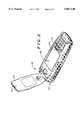
- FIG. 1is a front, top and side perspective view illustrating a device in a closed position.
- FIG. 2is a front, top and side perspective view illustrating the device according to FIG. 1 in an open position.
- FIG. 3is a circuit schematic in block diagram form illustrating a circuit in the device according to FIG. 1.
- FIG. 4is a circuit schematic in block diagram form illustrating a portion of the circuit according to FIG. 3.
- FIG. 5is a circuit schematic illustrating an alternate embodiment of the circuit according to FIG. 4.
- a device 100includes a display area 102, a keypad 104, an antenna 106, and a battery 112.
- the illustrated device 100is a portable communication device, and more particularly a cellular radiotelephone.
- the present inventionmay find application in other devices incorporating a display, such as a pager, a two-way radio, a calculator, a portable computer, a palm top computer, a personal digital assistant (PDA), a video recorder, or the like, and as used herein "device” includes each of these and their equivalents.
- a housing 107 of device 100includes a housing portion 108, which is illustrated to be a cover, and a housing portion 110, which is illustrated to be the body.
- the housing 107moves between a closed position (FIG. 1) and an open position (FIG. 2).
- the cover 108 and body 110are movingly interconnected by any suitable connector, such as a hinge, a rail assembly facilitating sliding, or the like.
- the housing 107is opened to expose the full viewing area of display panel 200 to a user.
- the display area 102 of the cover 108can be provided by a lens, such as a transparent polymeric element, or an opening that permits viewing of at least a portion of the display panel 200 while the cover 108 is closed.
- the lensis preferred as it protects the surface of display panel 200 when the cover is closed.
- the device 100includes a magnet 202 in the cover 108 and a reed switch 204 in the body 110.
- the magnet and reed switchprovide a sensor for detecting the open and closed positions of the housing 107.
- the sensorcan be provided by any hall effect device, a mechanical switch, an optical device, or the like, and "sensor" as used herein refers to each of these and their equivalents.
- a display system 300(FIG. 3) is housed within body 110.
- the display system 300generally includes a display control circuit 301 coupled to a display panel 200.
- the illustrated display panel 200has a full display screen area 303, which is the entire viewable display area of the display panel screen. It also includes a partial display field 305 which is within, but smaller than, the full display screen area 303.
- the partial display fieldmay be located in any region of the display screen, and it may be moved and/or its size altered, as will be described in greater detail herein below.
- the display panelcan have graphic capabilities.
- An exemplary displayhas a 15 level gray scale image provided by a 4 bit control signal for each pixel.
- the exemplary displayhas a full liquid crystal display (LCD) panel screen with a display area of 192 pixels by 272 pixels and a pitch of 120 dots/inch.
- LCDliquid crystal display
- the display panelcan be implemented by any conventional display panel such as those commercially available from Epson Corporation or Optrex.
- the display panel 200can be a single or multi-line display, monochrome or color.
- the display system 300comprises the display control circuit 301 and the display panel 200.
- the display control circuit 301comprises a central processing unit (CPU) 312 coupled to a display image buffer 304 and a display driver 310.
- the display driver 310includes a vertical, or column, driver 311 and a horizontal, or row, driver 313.
- the drivers 311 and 313control the voltages applied to the columns and rows of display panel responsive to signals from CPU 312.
- the driverscan be implemented with any suitable commercially available drivers, such as those manufactured by Sharp Corporation.
- the display image buffer 304stores an image for the display panel.
- the display image buffer 304is sufficiently large to store the required number of pixels to render an image over the entire area of display panel 200.
- the capacity in bytes of the display image buffer 304can be determined using the following:
- xnumber of pixels in a horizontal line
- ynumber of pixels in a vertical line.
- the total memory required to generate an image over the entire area of display panel 200is 26,112 bytes.
- a DRAM having a capacity of 2 Mbytescan be used to implement the buffer, and the buffer will be a portion of this memory.
- the rest of the DRAMcan be used for other purposes not related to the display.
- the display image buffer 304is easily accessible to the CPU 312 to permit dynamic movement, such as scrolling, of objects, such as icons, and real time plotting.
- the display image buffer 304is connected to the central processing unit (CPU) 312 by data bus 315.
- the CPU 312stores images in display image buffer 304 that are to be displayed on the full display screen area 303 of the display panel 200.
- Four bit control signals for each pixelare sequentially copied out of the display image buffer 304 and applied to the display driver 310 by CPU 312.
- the CPU 312may be implemented using any suitable commercially available controller, microprocessor, or digital signal processor (DSP), such as the CL-7110 commercially available from Cirrus Logic.
- the CPU 312receives inputs from the user input 314, which can include a touch pad (not shown) for display panel 200, keypad 104, other keys on the device, a microphone (not shown), or the like.
- the CPU 312also receives inputs from sensors 316, which can include reed switch 204, an ambient light sensor (not shown), or the like.
- the CPU 312may also include a software implemented sensor that monitors activity of the CPU and provides status information. Sensor as used herein includes all such detectors internal and external to the CPU and their equivalents.
- One of the sensorsis reed switch 204, which is closed when the cover 108 is open and open when the cover 108 is closed.
- the reed switch 204connects a voltage to CPU 312 when it is closed, which occurs when the magnet on the cover 108 is remote from the reed switch. The voltage is thus applied through the reed switch 204 to the CPU 312 when the cover is open and not when the cover 108 is closed.
- the CPU 312is thus responsive to the reed switch to sense whether the cover 108 is closed or open.
- the CPU 312also has an internal sensor (not shown) that detects inactivity. If the CPU 312 receives no inputs from the user input 314 and RF circuit 318 for a predetermined period of time, the CPU can enter a sleep mode.
- the CPU 312responds to these sensors 316 to control the display panel 200 to display an image only in the partial display field 305 when the phone enters a "sleep mode" due to inactivity of the processor, or when the phone is active while the cover 108 is closed.
- the full display modecan be automatically activated when the cover 108 is opened and the partial display mode can be automatically entered when the cover 108 is closed responsive to the inputs from the sensors.
- the CPU 312is coupled to display driver 310 by buses 317 and 319.
- the display driverincludes a horizontal driver 313 and a vertical driver 311.
- the horizontal driver 313controls the voltage input to the rows of pixels on the display panel 200.
- the vertical driver 311controls the voltage input to the columns of pixels of the display panel 200.
- the vertical driver 311 and horizontal driver 313can be implemented using any suitable commercially available drivers, such as those available from Sharp. These drivers receive pixel control signals from CPU 312 and output parallel control signals to the display panel 200.
- the illustrated portable communication deviceincludes a radio frequency (RF) circuit 318 coupled to an antenna 106 for communicating with a base station (not shown).
- the RF circuit 318communicates with CPU 312 over a bi-directional communication bus 320 and with a base station (not shown) via antenna 106.
- the RF circuit and antenna 106can be implemented using any suitable commercially available radio frequency circuitry.
- the display system 300is powered by battery 112.
- the battery voltageis regulated by voltage regulator 322.
- the amount of power drawn by the display system 300impacts on the amount of time that it will take to deplete the battery 112. It is therefore desirable to reduce the power consumption of portable device 100 by decreasing the power consumption of display system 300 to thereby increase the time that it takes to deplete the battery without increasing the size of the battery.
- the CPU 312 of FIG. 3includes an image control circuit 400 having a direct memory access (DMA) channel 406, a control circuit 409, a first-in-first-out (FIFO) memory 416, and a pixel fill circuit 418.
- the control circuit 409includes an input switch 414, an output switch 420, and state control and timing logic 422.
- the DMA channel 406copies pixel control signals from the display image buffer.
- the DMA channelsequentially copies 4 bit pixel control signals from the display image buffer 304 and loads them into input switch 414.
- the DMA channelpreferably has a bit width that matches the width of display image buffer 304, data bus 315 and FIFO memory 416.
- the input switch 414has an input contact 426 connected to receive the sequential pixel control signals from the DMA channel 406 output. Another input contact 428 is connected to receive an output of the FIFO memory 416. A control input 432 receives a control signal responsive to which input contact 426 or input contact 428 is selected to be connected to an output 430 of output switch 420.
- the input switch 414can be implemented using any suitable switching element, such as a digital switch employing logic gates, an analog switch using transistor elements, an electromechanical switch, software commands in the core of CPU 312, or the like.
- the FIFO memory 416receives the sequential pixel control signals from the output 430 of input switch 414 at an input 431.
- the FIFO memory 416outputs signals at output 433 in the same order as they are received at input 431.
- the FIFO memory 416contains "n" locations, where n is equal to the number of pixels of display panel 200 used in the partial display operating mode, which is the number of pixels in the partial display field 305.
- each pixel control signal in FIFO memory 416comprises 4 bits associated with a pixel having 15 gray scale levels. If the partial display field, or area, 305 has 120 pixels, the FIFO memory 416 has 120 locations of 4 bits each.
- FIFO memory 416need only store 120 locations of 1 bit each to generate an image over 120 pixels. It is envisioned that for the case when the cover 108 is closed, a monochrome image will be generated as the images are alphanumeric, such as text and phone numbers, which are well suited to a monochrome image.
- the FIFO memory 416is used to guarantee that a steady, continuous stream of pixel data is available for the pixel scanning controller 424 to insure that the image on the display panel 200 does not flicker.
- the DMA channel 406which shares access privileges for the display image buffer 304 and the data bus 315 with the core of CPU 312, moves pixel control signals only while it has access to the data channel.
- the DMA channelloads the FIFO memory 416 at a rate faster than the contents are read out by pixel scanning controller 424 during these access periods.
- the FIFO memory 416is thus loaded to prevent under-run by temporarily storing pixel elements in the full display operating mode.
- the input switch 414In the partial image display mode, the input switch 414 is held in position b, wherein the input contact 428 is connected to the output 430. This allows the contents of the FIFO memory 416 to circulate while the DMA channel 406, and optionally the display image buffer 304, are disabled (powered down). This provides significant power savings in the partial display mode. In the partial display operating mode, the FIFO memory 416 thus stores all of the pixel control signals for the partial image.
- the output switch 420is identical to the input switch 414. It includes an input contact 440 connected to the output 433 of FIFO memory 416, an input contact 442 coupled to a pixel fill circuit 418 and an output 444 connected to pixel scanning controller 424. A control signal for controlling the position of output switch 420 is input at control input 446.
- the pixel fill circuit 418supplies a continuous stream of pixel samples all having the same value.
- the value of each pixelis selected to render a pixel off condition, which is a blank image, on the display panel 200 in the rows and columns of the display outside of the partial display field 305.
- a data flip-flop 460has a data input connected to the CPU data bus to receive logic 0 and logic 1 signals therefrom.
- the clock input of the data flip-flopsets the register clock rate, and this input is connected to the CPU which provides a write enable signal thereto.
- the data flip-flopis programmed to output a sequence of zeros, ones, or a combination thereof, as required to produce a logic off signal for pixels of the display panel 200, by controlling the logic level at the D input to the data flip-flop.
- the rate at which pixel off signals are outputis controlled by the register clock rate, such that the pixel fill circuit 418 can be controlled, or "programmed", according to the requirements of any commercially available display panel.
- the actual value of the sampleis programmable to accommodate different types of LCD driver circuits.
- the pixel fill circuit 418can be implemented with a register storing a pixel off signal, such as a logic 0, which is output to the driver with each clock pulse.
- the registercan be a clocked flip-flop as described above, a clocked register, or the like.
- the state control and timing logic 422comprises the logic for the generation of timing signals for the DMA channel and the pixel scanning controller 424, and coordinates the timely switching of the input switch 414 and the output switch 420.
- the timing state control and timing logic 422controls the size and aspect ratio of the displayed image used in the partial display mode, and selection of the active operating mode, by controlling the input switch 414 and output switch 420.
- the state control and timing logic 422can be implemented in the core of the CPU 312, in registers outside of the core, or the like.
- the pixel scanning controllercan also include a small FIFO buffer (not shown) storing for example 16 bytes.
- Pixel scanningis controlled by a pixel scanning controller 424.
- the pixel scanning controller 424converts the pixel information supplied at the output 444 of output switch 420 into a signal for application to the horizontal driver 313 and vertical driver 311.
- the conversion processincludes gray scale interpretation of the pixel signal used to control the duty cycle (on time/off-time) of the coded pixel data.
- Any conventional pixel scanning controllercan be used to implement pixel scanning controller 424, such as commercially available LCD controllers or the like.
- the display systemoperates in a partial display mode, wherein only partial display field 305 displays an image, and a full display mode, wherein the full display screen area 303 of display panel 200 displays an image.
- An image which occupies the entire displayis stored in display image buffer 304. Smaller images that occupy only a portion of the display area are loaded into FIFO memory 416 just prior to initiation of the partial display mode.
- the image in FIFO memory 416is a two dimensional array with each element in the array representing a pixel.
- a pixel element in the arraycan represent up to 15 shades of grey.
- the CPU 312has ready access to the display image buffer and the image contained in the buffer is coded properly according to known techniques.
- the DMA channel 406is used to access the display image buffer 304 and deliver pixel signals, organized into groups of 8 or 16 bit words, to the input of FIFO memory 416 through the input switch 414. If 8 bit words are loaded, two pixel signals are loaded side by side. If 16 bit words are loaded, four pixel signals are loaded side-by side. Each time the FIFO memory 416 is half empty, the DMA channel 406 is signaled to retrieve additional samples from the display image buffer 304 and write these words into FIFO memory 416 until it is filled. The DMA channel 406 thus loads the FIFO memory 416 with sufficient data to avoid flickering.
- the DMA channel 406is provided with the appropriate logic to access the samples from the image buffer in a linear and sequential manner and present these samples in sequential order to the FIFO memory 416.
- the state control logicconfigures output switch 420 into position a, with input contact 440 connected to output 444, throughout the full display operating mode.
- the samples loaded into FIFO memory 416 by the DMA channel 406advance towards the output side of the FIFO memory 416 as the pixel scanning controller 424 reads each sample from the FIFO memory 416 in succession.
- the pixel scanning controller 424receives a timing clock signal from the state control and timing logic 422 and uses the clock signal to convert the parallel pixel words from FIFO memory 416 into a sequential stream of pixel sets to be applied to the rows and columns of display panel 200 via horizontal driver 313 and vertical driver 311, respectively.
- Pixels which are coded for gray scale operationare processed to render a shade of grey appropriate with an assigned value by controlling the duty cycle of the coded pixel data as is known in the art. Intermediate shades of grey are produced by varying the pixel-on to pixel-off ratio for several frames. It will be recognized by those skilled in the art that the display contrast is achieved by varying the supply voltage responsive to ambient light sensors and ambient temperature detectors to thereby render the best contrast for indoor and outdoor lighting.
- the pixel scanning controller 424is programmed to signal the horizontal driver 313 and vertical driver 311 when a new horizontal line of pixels is being output or when the bottom of the display panel 200 has been reached the scanning process will restart from the top.
- the partial display modeis activated by connecting the input switch 414 to the output of FIFO memory 416 such that the contents of the FIFO memory 416 is recirculated.
- the input switch 414remains in this position throughout the partial display mode.
- the contents of the FIFO memory 416is thus recirculated as it is systematically copied into the pixel scanning controller 424.
- This modeeliminates the necessity to operate the DMA channel 406 and the repeated DMA accesses to the large display image buffer 304.
- the DMA channel 406 and the display image buffer 304can be powered down, which results in a considerable reduction in power consumption.
- the input switchis moved from input contact 426 to input contact 428 when the first pixel of the first row to be displayed in the top of partial display field 305 is at the output of FIFO memory 416. This assures the image to be displayed recirculates and the desired partial display mode image is correct.
- the aspect ratio of the imagewhich is the horizontal to vertical dimensions, is determined by logic provided in the state controller.
- the output switch 420is controlled to connect the input contact 442 to the pixel fill circuit 418 during periods when the pixel scanning controller 424 is scanning the unused portions of the display panel.
- the output switch 420thus acts as a combiner to combine the pixel off signals with the partial image pixel control signals to control all of the display screen area of display panel 200 during the partial display mode.
- Other combinerscan be used in place of output switch 420, such as software control of the FIFO memory 416 and the pixel fill circuit 418 to insert signals onto a common bus in the appropriate order, or the like.
- the combiner, output switch 420assures the region outside of partial display field 305 is controlled by the pixel fill bits, which are pixel off control signals. Scanning the display with pixel off signals protects the display panel 200 against plasma affect damage by insuring that an AC signal is applied to all pixels under all conditions of operation.
- the pixel scanning controller 424 and drivers 311 and 313provide an alternating voltage to the display panel 200 to insure that an AC voltage is always applied to the display panel 200.
- the partial display modeprovides energy conservation by reducing the power drawn by the display system 300.
- a pixel off codeis scanned over the unused portion of the display to assure that the unused portion remains blank.
- the size of the partial display areais determined by the size of the FIFO memory 416 and the number of bits used to represent a single pixel element (i.e., the gray scale).
- Preferably 1 bit pixel words (monochrome)are used in the partial display mode to provide significant memory savings, and because the information displayed will be principally telephone number and text information which is well suited to monochrome display.
- the control of the blanked rows and columns and the insertion of the FIFO memory 416 pixelscontrols the location of the partial display field 305.
- the image that is generatedcan be located in any region of the display.
- the rows and columns of the remainder of the displayare controlled to be off thereby providing a reduction in power consumption.
- An alternate image control circuit 501includes a partial image memory 500 (FIG. 5) and a control circuit 509.
- the partial image memory 500is loaded with a partial image signal from CPU 312 on data bus 315.
- the partial image memory 500can be implemented using any suitable memory device, such as static random access memory (SRAM).
- the CPU 312loads pixel control signals for the partial display field 305 into the partial image memory 500 via data bus 315 at the beginning of the partial display mode.
- the input contact 428 of input switch 414is connected to the output of partial image memory 500.
- the partial imageis then input to the pixel scanning controller 424 through output switch 420.
- the pixel control signalsare read out in sequential order by increasing the address input to the partial image memory on each clock signal.
- the SRAMcan for example be organized as 512 locations of 32 bits each. Each element stores a signal binary digit. In 1 bit/pixel mode (i.e., monochrome operation) this corresponds to 1 pixel per array element. If 4 bit gray scale is employed the image capable of being rendered is reduced by a factor of four.
- the output 444 of output switch 420is connected to input contact 442, when the pixel scanning controller is reading pixel control signals for the rows and columns to be blank such that the pixel scanning controller receives the pixel off signal at the appropriate time.
- the partial display fieldcan be placed at any region of the full display screen area 303 by selecting the rows and columns to be controlled by the pixel off signal.
- the pixel scanning controller 424can include a DMA channel (not shown), for accessing the partial image memory 500, and a small FIFO buffer (not shown), used while unloading the contents of the partial image memory 500.
- the data bus 315can for example be 16 bits wide, and the pseudo DMA channel can fetch eight 16 bit words at a time to copy into the small FIFO buffer.
- the pixel scanning controller 424is responsive thereto to control the vertical driver 311 and horizontal driver 313 to display an image during the partial display mode.
- the display control circuit 301thus includes a first display image buffer 304 having capacity sufficient to store pixel control signals for controlling the image on the entire display screen of the display panel 200.
- a second display image buffer, FIFO memory 416 or partial image memory 500has the capacity to hold an image for the partial display field 305.
- the second display image bufferis smaller than the first display image buffer.
- the state control and timing logic 422controls the operation of the input switch 414 and output switch 420 such that the source of the image for the screen is switched from the first display image buffer to the second display image buffer in a synchronized manner.
- the pixel fill circuit 418stores a pixel off signal controlling the portion of the display outside of the partial display field to be off.
- the pixel off signal valuecan be selected to match the requirements of the display driver 310 and display panel 200. Additionally, the output switch 420 can be controlled so as to blank different rows and columns, thus changing the location of the partial display field 305. By changing the blanked columns and rows, the partial display field sourced from the second buffer can be placed in different areas of the display screen.
- the partial display modethus provides significant power savings, which is particularly important in battery powered devices. This power savings is accomplished without detrimentally impacting upon the operation of the display system in the full display operating mode.
Landscapes
- Engineering & Computer Science (AREA)
- Signal Processing (AREA)
- Theoretical Computer Science (AREA)
- Physics & Mathematics (AREA)
- Computer Hardware Design (AREA)
- General Physics & Mathematics (AREA)
- Computer Graphics (AREA)
- Human Computer Interaction (AREA)
- Computer Networks & Wireless Communication (AREA)
- Chemical & Material Sciences (AREA)
- Crystallography & Structural Chemistry (AREA)
- Control Of Indicators Other Than Cathode Ray Tubes (AREA)
- Liquid Crystal Display Device Control (AREA)
- Liquid Crystal (AREA)
Abstract
Description
The present invention pertains to displays, and more particularly to circuits for controlling the signal applied to a display panel.
Display systems, such as liquid crystal display (LCD) systems, have been implemented using a central processing unit (CPU), a display image buffer, and a display driver driving a display panel. For large screen LCD displays, the CPU operates to copy data from the display image buffer and apply the data to the display driver in a pixel-by-pixel manner. The driver produces a voltage on the display panel that controls the pixels thereon to have a particular intensity and decay rate. The process of applying a voltage is done repeatedly, at timed intervals, and is known in the art as "refreshing the display."
Display systems for small panels require a proportionally smaller display image buffer than systems for larger display panels. Many systems for small display panels implement the display image buffer in the same integrated circuit (IC) as the logic circuitry for controlling the display panel, such buffer known as an internal buffer. This approach yields a much lower current drain than using an external memory device for the display image buffer. However, the size of the display panel that can be driven by the integrated buffer is limited by the die area available for the display image buffer on the IC. Another drawback with this approach is CPU access to the internal display image buffer is restricted. Because access is restricted, as the display gets bigger the CPU has a more difficult time changing the contents of the internal display image buffer fast enough to avoid flicker and hesitation during scrolling. Consequently, for display systems employing an internal buffer for a large display panel, it is difficult to scroll images on the display panel in a smooth consistent manner.
It is therefor desirable to provide a system for controlling a large display with improved current drain characteristics.
FIG. 1 is a front, top and side perspective view illustrating a device in a closed position.
FIG. 2 is a front, top and side perspective view illustrating the device according to FIG. 1 in an open position.
FIG. 3 is a circuit schematic in block diagram form illustrating a circuit in the device according to FIG. 1.
FIG. 4 is a circuit schematic in block diagram form illustrating a portion of the circuit according to FIG. 3.
FIG. 5 is a circuit schematic illustrating an alternate embodiment of the circuit according to FIG. 4.
Adevice 100 includes adisplay area 102, akeypad 104, anantenna 106, and abattery 112. The illustrateddevice 100 is a portable communication device, and more particularly a cellular radiotelephone. However, the present invention may find application in other devices incorporating a display, such as a pager, a two-way radio, a calculator, a portable computer, a palm top computer, a personal digital assistant (PDA), a video recorder, or the like, and as used herein "device" includes each of these and their equivalents.
Ahousing 107 ofdevice 100 includes ahousing portion 108, which is illustrated to be a cover, and ahousing portion 110, which is illustrated to be the body. Thehousing 107 moves between a closed position (FIG. 1) and an open position (FIG. 2). Thecover 108 andbody 110 are movingly interconnected by any suitable connector, such as a hinge, a rail assembly facilitating sliding, or the like. Thehousing 107 is opened to expose the full viewing area ofdisplay panel 200 to a user.
Thedisplay area 102 of thecover 108 can be provided by a lens, such as a transparent polymeric element, or an opening that permits viewing of at least a portion of thedisplay panel 200 while thecover 108 is closed. The lens is preferred as it protects the surface ofdisplay panel 200 when the cover is closed. Thedevice 100 includes a magnet 202 in thecover 108 and areed switch 204 in thebody 110. The magnet and reed switch provide a sensor for detecting the open and closed positions of thehousing 107. The sensor can be provided by any hall effect device, a mechanical switch, an optical device, or the like, and "sensor" as used herein refers to each of these and their equivalents.
A display system 300 (FIG. 3) is housed withinbody 110. Thedisplay system 300 generally includes adisplay control circuit 301 coupled to adisplay panel 200. The illustrateddisplay panel 200 has a fulldisplay screen area 303, which is the entire viewable display area of the display panel screen. It also includes apartial display field 305 which is within, but smaller than, the fulldisplay screen area 303. The partial display field may be located in any region of the display screen, and it may be moved and/or its size altered, as will be described in greater detail herein below.
The display panel can have graphic capabilities. An exemplary display has a 15 level gray scale image provided by a 4 bit control signal for each pixel. The exemplary display has a full liquid crystal display (LCD) panel screen with a display area of 192 pixels by 272 pixels and a pitch of 120 dots/inch. However, the size of the display is not critical, and those skilled in the art will recognize that the display panel can have other sizes. The display panel can be implemented by any conventional display panel such as those commercially available from Epson Corporation or Optrex. Thedisplay panel 200 can be a single or multi-line display, monochrome or color.
Thedisplay system 300 comprises thedisplay control circuit 301 and thedisplay panel 200. Thedisplay control circuit 301 comprises a central processing unit (CPU) 312 coupled to adisplay image buffer 304 and adisplay driver 310. Thedisplay driver 310 includes a vertical, or column,driver 311 and a horizontal, or row,driver 313. Thedrivers CPU 312. The drivers can be implemented with any suitable commercially available drivers, such as those manufactured by Sharp Corporation.
Thedisplay image buffer 304 stores an image for the display panel. Thedisplay image buffer 304 is sufficiently large to store the required number of pixels to render an image over the entire area ofdisplay panel 200. The capacity in bytes of thedisplay image buffer 304 can be determined using the following:
bytes=G*x*y/8
where bytes=the capacity of the memory in bytes; G=the number of bits per pixel (1=monochrome; 2=4 level gray scale; 4=15 level gray scale);
x=number of pixels in a horizontal line;
y=number of pixels in a vertical line.
For example, for a display having 192 pixel columns, 272 pixel rows, and 15 level gray scale, the total memory required to generate an image over the entire area ofdisplay panel 200 is 26,112 bytes. To condense parts, a DRAM having a capacity of 2 Mbytes can be used to implement the buffer, and the buffer will be a portion of this memory. The rest of the DRAM can be used for other purposes not related to the display. Thedisplay image buffer 304 is easily accessible to theCPU 312 to permit dynamic movement, such as scrolling, of objects, such as icons, and real time plotting.
Thedisplay image buffer 304 is connected to the central processing unit (CPU) 312 bydata bus 315. TheCPU 312 stores images indisplay image buffer 304 that are to be displayed on the fulldisplay screen area 303 of thedisplay panel 200. Four bit control signals for each pixel are sequentially copied out of thedisplay image buffer 304 and applied to thedisplay driver 310 byCPU 312. TheCPU 312 may be implemented using any suitable commercially available controller, microprocessor, or digital signal processor (DSP), such as the CL-7110 commercially available from Cirrus Logic.
TheCPU 312 receives inputs from theuser input 314, which can include a touch pad (not shown) fordisplay panel 200,keypad 104, other keys on the device, a microphone (not shown), or the like. TheCPU 312 also receives inputs fromsensors 316, which can includereed switch 204, an ambient light sensor (not shown), or the like. TheCPU 312 may also include a software implemented sensor that monitors activity of the CPU and provides status information. Sensor as used herein includes all such detectors internal and external to the CPU and their equivalents.
One of the sensors isreed switch 204, which is closed when thecover 108 is open and open when thecover 108 is closed. Thereed switch 204 connects a voltage toCPU 312 when it is closed, which occurs when the magnet on thecover 108 is remote from the reed switch. The voltage is thus applied through thereed switch 204 to theCPU 312 when the cover is open and not when thecover 108 is closed. TheCPU 312 is thus responsive to the reed switch to sense whether thecover 108 is closed or open.
TheCPU 312 also has an internal sensor (not shown) that detects inactivity. If theCPU 312 receives no inputs from theuser input 314 andRF circuit 318 for a predetermined period of time, the CPU can enter a sleep mode.
TheCPU 312 responds to thesesensors 316 to control thedisplay panel 200 to display an image only in thepartial display field 305 when the phone enters a "sleep mode" due to inactivity of the processor, or when the phone is active while thecover 108 is closed. The full display mode can be automatically activated when thecover 108 is opened and the partial display mode can be automatically entered when thecover 108 is closed responsive to the inputs from the sensors.
TheCPU 312 is coupled to displaydriver 310 bybuses horizontal driver 313 and avertical driver 311. Thehorizontal driver 313 controls the voltage input to the rows of pixels on thedisplay panel 200. Thevertical driver 311 controls the voltage input to the columns of pixels of thedisplay panel 200. Thevertical driver 311 andhorizontal driver 313 can be implemented using any suitable commercially available drivers, such as those available from Sharp. These drivers receive pixel control signals fromCPU 312 and output parallel control signals to thedisplay panel 200.
In addition to thedisplay system 300, the illustrated portable communication device includes a radio frequency (RF)circuit 318 coupled to anantenna 106 for communicating with a base station (not shown). TheRF circuit 318 communicates withCPU 312 over abi-directional communication bus 320 and with a base station (not shown) viaantenna 106. The RF circuit andantenna 106 can be implemented using any suitable commercially available radio frequency circuitry.
Thedisplay system 300 is powered bybattery 112. The battery voltage is regulated byvoltage regulator 322. Those skilled in the art will recognize that the amount of power drawn by thedisplay system 300 impacts on the amount of time that it will take to deplete thebattery 112. It is therefore desirable to reduce the power consumption ofportable device 100 by decreasing the power consumption ofdisplay system 300 to thereby increase the time that it takes to deplete the battery without increasing the size of the battery.
With reference now to FIG. 4, theCPU 312 of FIG. 3 includes animage control circuit 400 having a direct memory access (DMA)channel 406, acontrol circuit 409, a first-in-first-out (FIFO)memory 416, and apixel fill circuit 418. Thecontrol circuit 409 includes aninput switch 414, anoutput switch 420, and state control andtiming logic 422. TheDMA channel 406 copies pixel control signals from the display image buffer. During times in which the core ofCPU 312 is not employing thedata bus 315 for operations other than operating the display, the DMA channel sequentially copies 4 bit pixel control signals from thedisplay image buffer 304 and loads them intoinput switch 414. The DMA channel preferably has a bit width that matches the width ofdisplay image buffer 304,data bus 315 andFIFO memory 416. By using a wider bus, the number of total fetches to retrieve the pixel control signals for an image is reduced, which increases the opportunity that theCPU 312 has to access the memory for loading an image or for other purposes. This provides the highest likelihood of realizing smooth scrolling of images.
Theinput switch 414 has aninput contact 426 connected to receive the sequential pixel control signals from theDMA channel 406 output. Anotherinput contact 428 is connected to receive an output of theFIFO memory 416. Acontrol input 432 receives a control signal responsive to whichinput contact 426 orinput contact 428 is selected to be connected to anoutput 430 ofoutput switch 420. Theinput switch 414 can be implemented using any suitable switching element, such as a digital switch employing logic gates, an analog switch using transistor elements, an electromechanical switch, software commands in the core ofCPU 312, or the like.
TheFIFO memory 416 receives the sequential pixel control signals from theoutput 430 ofinput switch 414 at aninput 431. TheFIFO memory 416 outputs signals atoutput 433 in the same order as they are received atinput 431. TheFIFO memory 416 contains "n" locations, where n is equal to the number of pixels ofdisplay panel 200 used in the partial display operating mode, which is the number of pixels in thepartial display field 305. For example, each pixel control signal inFIFO memory 416 comprises 4 bits associated with a pixel having 15 gray scale levels. If the partial display field, or area, 305 has 120 pixels, theFIFO memory 416 has 120 locations of 4 bits each. By using a single bit per pixel, additional memory size savings can be achieved as theFIFO memory 416 need only store 120 locations of 1 bit each to generate an image over 120 pixels. It is envisioned that for the case when thecover 108 is closed, a monochrome image will be generated as the images are alphanumeric, such as text and phone numbers, which are well suited to a monochrome image.
TheFIFO memory 416 is used to guarantee that a steady, continuous stream of pixel data is available for thepixel scanning controller 424 to insure that the image on thedisplay panel 200 does not flicker. TheDMA channel 406, which shares access privileges for thedisplay image buffer 304 and thedata bus 315 with the core ofCPU 312, moves pixel control signals only while it has access to the data channel. The DMA channel loads theFIFO memory 416 at a rate faster than the contents are read out bypixel scanning controller 424 during these access periods. TheFIFO memory 416 is thus loaded to prevent under-run by temporarily storing pixel elements in the full display operating mode. Under-run occurs when the buffer is not loaded with enough samples for thepixel scanning controller 424 to read, causing the pixel scanning controller to ignore pixels, which results in jumping during scrolling and image flicker. If for any reason the DMA channel doesn't supply a pixel control signal in a timely manner, the output of theFIFO memory 416 can be recirculated back to theinput 431 byinput switch 414.
In the partial image display mode, theinput switch 414 is held in position b, wherein theinput contact 428 is connected to theoutput 430. This allows the contents of theFIFO memory 416 to circulate while theDMA channel 406, and optionally thedisplay image buffer 304, are disabled (powered down). This provides significant power savings in the partial display mode. In the partial display operating mode, theFIFO memory 416 thus stores all of the pixel control signals for the partial image.
Theoutput switch 420 is identical to theinput switch 414. It includes aninput contact 440 connected to theoutput 433 ofFIFO memory 416, aninput contact 442 coupled to apixel fill circuit 418 and anoutput 444 connected topixel scanning controller 424. A control signal for controlling the position ofoutput switch 420 is input at control input 446.
Thepixel fill circuit 418 supplies a continuous stream of pixel samples all having the same value. The value of each pixel is selected to render a pixel off condition, which is a blank image, on thedisplay panel 200 in the rows and columns of the display outside of thepartial display field 305. A data flip-flop 460 has a data input connected to the CPU data bus to receivelogic 0 andlogic 1 signals therefrom. The clock input of the data flip-flop sets the register clock rate, and this input is connected to the CPU which provides a write enable signal thereto. The data flip-flop is programmed to output a sequence of zeros, ones, or a combination thereof, as required to produce a logic off signal for pixels of thedisplay panel 200, by controlling the logic level at the D input to the data flip-flop. The rate at which pixel off signals are output is controlled by the register clock rate, such that thepixel fill circuit 418 can be controlled, or "programmed", according to the requirements of any commercially available display panel.
The actual value of the sample is programmable to accommodate different types of LCD driver circuits. Thepixel fill circuit 418 can be implemented with a register storing a pixel off signal, such as alogic 0, which is output to the driver with each clock pulse. The register can be a clocked flip-flop as described above, a clocked register, or the like.
The state control andtiming logic 422 comprises the logic for the generation of timing signals for the DMA channel and thepixel scanning controller 424, and coordinates the timely switching of theinput switch 414 and theoutput switch 420. The timing state control andtiming logic 422 controls the size and aspect ratio of the displayed image used in the partial display mode, and selection of the active operating mode, by controlling theinput switch 414 andoutput switch 420. The state control andtiming logic 422 can be implemented in the core of theCPU 312, in registers outside of the core, or the like. The pixel scanning controller can also include a small FIFO buffer (not shown) storing for example 16 bytes.
Pixel scanning is controlled by apixel scanning controller 424. Thepixel scanning controller 424 converts the pixel information supplied at theoutput 444 ofoutput switch 420 into a signal for application to thehorizontal driver 313 andvertical driver 311. The conversion process includes gray scale interpretation of the pixel signal used to control the duty cycle (on time/off-time) of the coded pixel data. Any conventional pixel scanning controller can be used to implementpixel scanning controller 424, such as commercially available LCD controllers or the like.
In operation, the display system operates in a partial display mode, wherein onlypartial display field 305 displays an image, and a full display mode, wherein the fulldisplay screen area 303 ofdisplay panel 200 displays an image. An image which occupies the entire display is stored indisplay image buffer 304. Smaller images that occupy only a portion of the display area are loaded intoFIFO memory 416 just prior to initiation of the partial display mode.
The image inFIFO memory 416 is a two dimensional array with each element in the array representing a pixel. A pixel element in the array can represent up to 15 shades of grey. For the purposes of these description, theCPU 312 has ready access to the display image buffer and the image contained in the buffer is coded properly according to known techniques.
In the full display mode, theinput switch 414 continues to connectinput contact 426 andoutput 430. TheDMA channel 406 is used to access thedisplay image buffer 304 and deliver pixel signals, organized into groups of 8 or 16 bit words, to the input ofFIFO memory 416 through theinput switch 414. If 8 bit words are loaded, two pixel signals are loaded side by side. If 16 bit words are loaded, four pixel signals are loaded side-by side. Each time theFIFO memory 416 is half empty, theDMA channel 406 is signaled to retrieve additional samples from thedisplay image buffer 304 and write these words intoFIFO memory 416 until it is filled. TheDMA channel 406 thus loads theFIFO memory 416 with sufficient data to avoid flickering. TheDMA channel 406 is provided with the appropriate logic to access the samples from the image buffer in a linear and sequential manner and present these samples in sequential order to theFIFO memory 416.
The state control logic configuresoutput switch 420 into position a, withinput contact 440 connected tooutput 444, throughout the full display operating mode. The samples loaded intoFIFO memory 416 by theDMA channel 406 advance towards the output side of theFIFO memory 416 as thepixel scanning controller 424 reads each sample from theFIFO memory 416 in succession.
Thepixel scanning controller 424 receives a timing clock signal from the state control andtiming logic 422 and uses the clock signal to convert the parallel pixel words fromFIFO memory 416 into a sequential stream of pixel sets to be applied to the rows and columns ofdisplay panel 200 viahorizontal driver 313 andvertical driver 311, respectively. Pixels which are coded for gray scale operation are processed to render a shade of grey appropriate with an assigned value by controlling the duty cycle of the coded pixel data as is known in the art. Intermediate shades of grey are produced by varying the pixel-on to pixel-off ratio for several frames. It will be recognized by those skilled in the art that the display contrast is achieved by varying the supply voltage responsive to ambient light sensors and ambient temperature detectors to thereby render the best contrast for indoor and outdoor lighting. In addition thepixel scanning controller 424 is programmed to signal thehorizontal driver 313 andvertical driver 311 when a new horizontal line of pixels is being output or when the bottom of thedisplay panel 200 has been reached the scanning process will restart from the top.
The partial display mode is activated by connecting theinput switch 414 to the output ofFIFO memory 416 such that the contents of theFIFO memory 416 is recirculated. Theinput switch 414 remains in this position throughout the partial display mode. The contents of theFIFO memory 416 is thus recirculated as it is systematically copied into thepixel scanning controller 424. This mode eliminates the necessity to operate theDMA channel 406 and the repeated DMA accesses to the largedisplay image buffer 304. TheDMA channel 406 and thedisplay image buffer 304 can be powered down, which results in a considerable reduction in power consumption.
The input switch is moved frominput contact 426 to inputcontact 428 when the first pixel of the first row to be displayed in the top ofpartial display field 305 is at the output ofFIFO memory 416. This assures the image to be displayed recirculates and the desired partial display mode image is correct.
The aspect ratio of the image, which is the horizontal to vertical dimensions, is determined by logic provided in the state controller. Theoutput switch 420 is controlled to connect theinput contact 442 to thepixel fill circuit 418 during periods when thepixel scanning controller 424 is scanning the unused portions of the display panel. Theoutput switch 420 thus acts as a combiner to combine the pixel off signals with the partial image pixel control signals to control all of the display screen area ofdisplay panel 200 during the partial display mode. Other combiners can be used in place ofoutput switch 420, such as software control of theFIFO memory 416 and thepixel fill circuit 418 to insert signals onto a common bus in the appropriate order, or the like.
Use of the combiner,output switch 420, assures the region outside ofpartial display field 305 is controlled by the pixel fill bits, which are pixel off control signals. Scanning the display with pixel off signals protects thedisplay panel 200 against plasma affect damage by insuring that an AC signal is applied to all pixels under all conditions of operation. Those skilled in the art will recognize that thepixel scanning controller 424 anddrivers display panel 200 to insure that an AC voltage is always applied to thedisplay panel 200.
The partial display mode provides energy conservation by reducing the power drawn by thedisplay system 300. A pixel off code is scanned over the unused portion of the display to assure that the unused portion remains blank. The size of the partial display area is determined by the size of theFIFO memory 416 and the number of bits used to represent a single pixel element (i.e., the gray scale). Preferably 1 bit pixel words (monochrome) are used in the partial display mode to provide significant memory savings, and because the information displayed will be principally telephone number and text information which is well suited to monochrome display. The control of the blanked rows and columns and the insertion of theFIFO memory 416 pixels controls the location of thepartial display field 305. By controlling the combination of pixel off signals with the contents of theFIFO memory 416 in the partial display mode, the image that is generated can be located in any region of the display. The rows and columns of the remainder of the display are controlled to be off thereby providing a reduction in power consumption.
An alternateimage control circuit 501 includes a partial image memory 500 (FIG. 5) and acontrol circuit 509. Thepartial image memory 500 is loaded with a partial image signal fromCPU 312 ondata bus 315. Thepartial image memory 500 can be implemented using any suitable memory device, such as static random access memory (SRAM).
In operation, theCPU 312 loads pixel control signals for thepartial display field 305 into thepartial image memory 500 viadata bus 315 at the beginning of the partial display mode. Theinput contact 428 ofinput switch 414 is connected to the output ofpartial image memory 500. The partial image is then input to thepixel scanning controller 424 throughoutput switch 420. The pixel control signals are read out in sequential order by increasing the address input to the partial image memory on each clock signal. The SRAM can for example be organized as 512 locations of 32 bits each. Each element stores a signal binary digit. In 1 bit/pixel mode (i.e., monochrome operation) this corresponds to 1 pixel per array element. If 4 bit gray scale is employed the image capable of being rendered is reduced by a factor of four. To blank those regions of the display outside of thepartial display field 305, theoutput 444 ofoutput switch 420 is connected to inputcontact 442, when the pixel scanning controller is reading pixel control signals for the rows and columns to be blank such that the pixel scanning controller receives the pixel off signal at the appropriate time. Those skilled in the art will recognize that the partial display field can be placed at any region of the fulldisplay screen area 303 by selecting the rows and columns to be controlled by the pixel off signal.
Thepixel scanning controller 424 can include a DMA channel (not shown), for accessing thepartial image memory 500, and a small FIFO buffer (not shown), used while unloading the contents of thepartial image memory 500. Thedata bus 315 can for example be 16 bits wide, and the pseudo DMA channel can fetch eight 16 bit words at a time to copy into the small FIFO buffer. Thepixel scanning controller 424 is responsive thereto to control thevertical driver 311 andhorizontal driver 313 to display an image during the partial display mode.
Thedisplay control circuit 301 thus includes a firstdisplay image buffer 304 having capacity sufficient to store pixel control signals for controlling the image on the entire display screen of thedisplay panel 200. A second display image buffer,FIFO memory 416 orpartial image memory 500, has the capacity to hold an image for thepartial display field 305. The second display image buffer is smaller than the first display image buffer. The state control andtiming logic 422 controls the operation of theinput switch 414 andoutput switch 420 such that the source of the image for the screen is switched from the first display image buffer to the second display image buffer in a synchronized manner. Thepixel fill circuit 418 stores a pixel off signal controlling the portion of the display outside of the partial display field to be off.
The pixel off signal value can be selected to match the requirements of thedisplay driver 310 anddisplay panel 200. Additionally, theoutput switch 420 can be controlled so as to blank different rows and columns, thus changing the location of thepartial display field 305. By changing the blanked columns and rows, the partial display field sourced from the second buffer can be placed in different areas of the display screen.
The partial display mode thus provides significant power savings, which is particularly important in battery powered devices. This power savings is accomplished without detrimentally impacting upon the operation of the display system in the full display operating mode.
Claims (23)
1. A display system comprising:
a display having a display with a display screen area upon which images can be generated for viewing; and
an image control circuit controlling operation of the display, the image control circuit controlling the display such that only a partial display area can be controlled to generate images in a first operating mode to conserve power and all of the display screen area can be controlled to generate images in a second operating mode;
wherein the image control circuit includes a first buffer storing pixel control signals for the partial display area, and the first buffer passes image control signals through to a pixel scanning controller in the second operating mode, and stores pixel control signals for the partial display area in the first operating mode.
2. The display system as defined in claim 1, including a display image buffer storing pixel control signals for all of the display screen area.
3. The display system as defined in claim 1, wherein the first buffer is a first-in-first-out memory.
4. The display system as defined in claim 3, further including a switch connecting an output of the first-in-first-out memory to an input of the first-in-first-out memory to circulate pixel control signals in a partial display mode.
5. The display system as defined in claim 4, wherein the switch connects the output to the input when a first pixel control signal of an image to appear in the partial display area is at the output of the first-in-first-out memory.
6. A display system comprising:
a display having a display with a display screen area upon which images can be generated for viewing; and
an image control circuit controlling operation of the display, the image control circuit controlling the display such that only a partial display area can be controlled to generate images in a first operating mode to conserve power and all of the display screen area can be controlled to generate images in a second operating mode;
wherein the image control circuit includes a first buffer storing pixel control signals for the partial display area, and an output of the first buffer is connected to a pixel scanning controller through a switch.
7. The display system as defined in claim 6 and further including a pixel fill circuit, the switch selectively connecting the pixel scanning controller to one of the output of the first buffer and an output of the pixel fill circuit, the pixel fill circuit generating pixel off signals, and the pixel off signals being input of the pixel scanning controller to select a location and size of the partial display area.
8. A battery powered device comprising:
a display having a display screen area;
a first display image buffer storing pixel control signals for all of the display screen area;
a second display image buffer, the second display image buffer being smaller than the first display image buffer, wherein the second display image buffer has sufficient capacity to store pixel control signals for only a portion of the display screen area; and
a control circuit to selectively provide pixel control signals from the first and second display image buffers to the display.
9. The battery powered device as defined in claim 8, wherein the control circuit includes a switch to selectively couple the second display image buffer to the first display image buffer.
10. The battery powered device as defined in claim 9, wherein the control circuit further includes a pixel fill circuit, the pixel fill circuit producing pixel off signals which are input to the display to blank the display screen area outside of the portion of the display screen area controlled by the second display image buffer.
11. The battery powered device as defined in claim 10, further comprising a register generating a value of the pixel off signals.
12. The battery powered device as defined in claim 10, wherein the control circuit includes a pixel scanning controller, the control circuit controlling insertion of the pixel off signals to the pixel scanning controller to blank rows and columns of pixels around the portion of the display screen area, and changing rows and columns of pixels that are to be blanked to relocate the portion of the display screen area in a new region of the display screen area.
13. The battery powered device as defined in claim 12 further including:
a first housing portion, the first housing portion comprising the display;
a second housing portion movingly carried on the first housing portion to move between an open and closed position, the second housing portion at least partially covering the first housing portion in the closed position; and
the control circuit responsive to the first and second housing portions being in a closed position to display an image only in the portion of the display screen area.
14. The battery powered device as defined in claim 8, wherein the control circuit is responsive to inactivity to control the portion of the display screen area to be the only region of the display screen area to display images to thereby conserve battery power.
15. An image control circuit comprising:
a pixel signal input;
a memory storing pixel signals for a portion of a display screen;
a pixel fill circuit outputting pixel off data; and
a control circuit coupled to the pixel signal input, the memory and the pixel fill circuit, the control circuit including a combiner selectively combining the pixel signals from the memory and the pixel off data, the combiner outputting an image sequence received at the pixel signal input in a full image mode and outputting pixel off data and pixel signals from the memory in a partial display mode;
further including a display image buffer storing pixel signals all of the display screen in a full display mode, the pixel signal input coupled to the display image buffer.
16. An image control circuit comprising:
a pixel signal input;
a memory storing pixel signals for a portion of a display screen;
a pixel fill circuit outputting pixel off data; and
a control circuit coupled to the pixel signal input, the memory and the pixel fill circuit, the control circuit including a combiner selectively combining the pixel signals from the memory and the pixel off data, the combiner outputting an image sequence received at the pixel signal input in a full image mode and outputting pixel off data and pixel signals from the memory in a partial display mode;
wherein the pixel fill circuit comprises a register storing pixel off signals.
17. The image control circuit as defined in claim 16, wherein the combiner comprises a first switch having an output, a first input coupled to the pixel fill circuit and a second input.
18. The image control circuit as defined in claim 17, wherein the control circuit further comprises a second switch having an output coupled to the second input of the first switch and an input coupled to the pixel signal input.
19. The image control circuit as defined in claim 18, further including a first-in-first-out buffer connected between the first switch and the second input of the second switch.
20. The image control circuit as defined in claim 18, further including a display image buffer coupled to another input of the second switch.
21. The image control circuit as defined in claim 18, wherein the control circuit further includes state control logic coupled to the first and second switches, the state control logic controlling a state of the first and second switches.
22. The image control circuit as defined in claim 21, further including a pixel scanning controller coupled to the output of the second switch and the state control logic.
23. The image control circuit as defined in claim 22, further including direct memory access channel coupled to the state control logic and the pixel signal input.
Priority Applications (7)
| Application Number | Priority Date | Filing Date | Title |
|---|---|---|---|
| US08/758,019US5867140A (en) | 1996-11-27 | 1996-11-27 | Display system and circuit therefor |
| FR9712474AFR2756404B1 (en) | 1996-11-27 | 1997-10-07 | DISPLAY SYSTEM AND CIRCUIT FOR THIS SYSTEM |
| GB9722300AGB2319878B (en) | 1996-11-27 | 1997-10-23 | Display system and circuit therefor |
| DE19751139.2ADE19751139B4 (en) | 1996-11-27 | 1997-11-19 | Display system and circuit for it |
| JP9369870AJPH10187106A (en) | 1996-11-27 | 1997-11-20 | Display system and its circuit |
| CN97120191ACN1102281C (en) | 1996-11-27 | 1997-11-24 | Display system and circuit therefor |
| KR1019970062979AKR100260695B1 (en) | 1996-11-27 | 1997-11-26 | Display system and circuit therefor |
Applications Claiming Priority (1)
| Application Number | Priority Date | Filing Date | Title |
|---|---|---|---|
| US08/758,019US5867140A (en) | 1996-11-27 | 1996-11-27 | Display system and circuit therefor |
Publications (1)
| Publication Number | Publication Date |
|---|---|
| US5867140Atrue US5867140A (en) | 1999-02-02 |
Family
ID=25050143
Family Applications (1)
| Application Number | Title | Priority Date | Filing Date |
|---|---|---|---|
| US08/758,019Expired - LifetimeUS5867140A (en) | 1996-11-27 | 1996-11-27 | Display system and circuit therefor |
Country Status (7)
| Country | Link |
|---|---|
| US (1) | US5867140A (en) |
| JP (1) | JPH10187106A (en) |
| KR (1) | KR100260695B1 (en) |
| CN (1) | CN1102281C (en) |
| DE (1) | DE19751139B4 (en) |
| FR (1) | FR2756404B1 (en) |
| GB (1) | GB2319878B (en) |
Cited By (93)
| Publication number | Priority date | Publication date | Assignee | Title |
|---|---|---|---|---|
| US6018331A (en)* | 1996-12-04 | 2000-01-25 | Nec Corporation | Frame display control in an image display having a liquid crystal display panel |
| US6075510A (en)* | 1997-10-28 | 2000-06-13 | Nortel Networks Corporation | Low power refreshing (smart display multiplexing) |
| US6115008A (en)* | 1998-02-12 | 2000-09-05 | Lear Automotive Dearborn, Inc. | Transparent EL display |
| US6137466A (en)* | 1997-11-03 | 2000-10-24 | Motorola, Inc. | LCD driver module and method thereof |
| US6137481A (en)* | 1996-12-12 | 2000-10-24 | Phillipps; John Quentin | Portable computer having power saving provisions |
| US6160541A (en)* | 1997-01-21 | 2000-12-12 | Lear Automotive Dearborn Inc. | Power consumption control for a visual screen display by utilizing a total number of pixels to be energized in the image to determine an order of pixel energization in a manner that conserves power |
| WO2001001323A1 (en)* | 1999-06-28 | 2001-01-04 | Interlogix, Inc. | Personal digital assistant key for an electronic lock |
| EP1052839A3 (en)* | 1999-05-13 | 2001-01-24 | Matsushita Electric Industrial Co., Ltd. | Terminal for mobile communication that can display text by switching between different character sets |
| US6181313B1 (en)* | 1997-01-30 | 2001-01-30 | Hitachi, Ltd. | Liquid crystal display controller and liquid crystal display device |
| US6311282B1 (en)* | 1996-02-27 | 2001-10-30 | Fujitsu Personal Systems, Inc. | Method and apparatus for computing device with status display |
| US6313832B1 (en)* | 1998-03-10 | 2001-11-06 | Fujitsu Limited | Remaining battery capacity display device |
| US6317313B1 (en) | 1999-11-09 | 2001-11-13 | Interlogix, Inc. | Case and cover for an electronic device |
| US20010052887A1 (en)* | 2000-04-11 | 2001-12-20 | Yusuke Tsutsui | Method and circuit for driving display device |
| EP1168143A1 (en)* | 2000-06-27 | 2002-01-02 | Koninklijke Philips Electronics N.V. | Portable computer comprising a plurality of display modules with at least one display module foldable over a main display module |
| US20020041278A1 (en)* | 2000-09-29 | 2002-04-11 | Seiko Epson Corporation | Electro-optical device and method of driving the same, organic electroluminescent display device, and electronic apparatus |
| EP1100067A3 (en)* | 1999-11-09 | 2002-07-10 | Matsushita Electric Industrial Co., Ltd. | Display unit and portable information terminal |
| EP1193681A3 (en)* | 2000-09-29 | 2002-07-31 | SANYO ELECTRIC Co., Ltd. | Driving device for display device |
| US20020111200A1 (en)* | 2001-02-09 | 2002-08-15 | Susumu Nikawa | Power reducing apparatus and method for portable terminal equipped with display unit |
| US20020126111A1 (en)* | 2001-03-09 | 2002-09-12 | Seiko Epson Corporation | Method of driving display elements and electronic apparatus using the driving method |
| US6466204B1 (en)* | 1999-01-13 | 2002-10-15 | Samsung Electronics, Co., Ltd. | Color LCD interface circuit in a portable radio terminal |
| US6476800B2 (en)* | 1998-03-23 | 2002-11-05 | International Business Machines Corporation | Method and apparatus for adjusting video refresh rate in response to power mode changes in order to conserve power |
| US20020171799A1 (en)* | 2001-04-30 | 2002-11-21 | Reiner Bayrle | LCD-cell |
| US20020175887A1 (en)* | 1998-02-09 | 2002-11-28 | Suguru Yamazaki | Electrooptical apparatus and driving method therefor, liquid crystal display apparatus and driving method therefor, electrooptical apparatus and driving circuit therefor, and electronic equipment |
| EP1211662A4 (en)* | 2000-04-05 | 2003-02-05 | Sony Corp | Display, method for driving the same, and portable terminal |
| US20030030633A1 (en)* | 2001-08-10 | 2003-02-13 | Au Optronics Corp. | Driving method for a power-saving Liquid Crystal Display |
| US6568590B2 (en)* | 1998-05-21 | 2003-05-27 | Matsushita Electric Industrial Co. | Electronic cash register and a method of displaying a processing result in an electronic cash register |
| US6577760B1 (en)* | 1997-12-18 | 2003-06-10 | Fuji Photo Film Co., Ltd. | Image processing apparatus and method, image synthesizing system and method, image synthesizer and client computer which constitute image synthesizing system, and image separating method |
| US20030132928A1 (en)* | 2002-01-09 | 2003-07-17 | Sony Corporation | Electronic apparatus and method and program of controlling the same |
| EP1215868A3 (en)* | 2000-12-14 | 2003-09-24 | Nokia Corporation | A mobile communication device with display mode control |
| US20030210215A1 (en)* | 2002-05-08 | 2003-11-13 | Hiroyuki Takahashi | Liquid crystal display device and driving method therefor |
| US20030222866A1 (en)* | 2002-05-30 | 2003-12-04 | Eastman Kodak Company | Display driver and method for driving an emissive video display in an image displaying device |
| US20040001049A1 (en)* | 2002-06-27 | 2004-01-01 | Oakley Nicholas W. | Multiple mode display apparatus |
| US20040027364A1 (en)* | 2001-09-19 | 2004-02-12 | Casio Computer Co., Ltd. | Display device and control system thereof |
| USD487066S1 (en) | 2002-09-09 | 2004-02-24 | Nokia Corporation | Handset |
| US20040155875A1 (en)* | 1999-03-24 | 2004-08-12 | Canon Kabushiki Kaisha | Flat-panel display apparatus and its control method |
| US20040199798A1 (en)* | 2003-04-03 | 2004-10-07 | Whelan Rochelle J. | Low power display refresh |
| US6809711B2 (en)* | 2001-05-03 | 2004-10-26 | Eastman Kodak Company | Display driver and method for driving an emissive video display |
| US20040217954A1 (en)* | 2003-05-01 | 2004-11-04 | O'gorman Patrick | Reduced power consumption for a graphics accelerator and display |
| US6822630B2 (en)* | 2000-03-02 | 2004-11-23 | Sharp Kabushiki Kaisha | Liquid crystal display device |
| US20040239665A1 (en)* | 2003-06-02 | 2004-12-02 | Katsushige Otsubo | Multiplex command on data line of digital interface display devices |
| US6888524B2 (en)* | 2000-02-24 | 2005-05-03 | Aeg Gesellschaft Fur Moderne Informationssysteme Mbh | Liquid crystal display device |
| US6886245B1 (en)* | 2001-11-09 | 2005-05-03 | Nokia Corporation | Method for manufacturing mobile electronic devices using a common engine assembly |
| US6900798B2 (en)* | 2001-08-31 | 2005-05-31 | Nokia Corporation | Power-conservation feature for liquid crystal display |
| US20050168468A1 (en)* | 2004-02-03 | 2005-08-04 | Sumita Rao | Mobile wireless device and a method for moving a graphical item on a mobile wireless device |
| US6934772B2 (en) | 1998-09-30 | 2005-08-23 | Hewlett-Packard Development Company, L.P. | Lowering display power consumption by dithering brightness |
| US20050185477A1 (en)* | 2004-02-25 | 2005-08-25 | Yoshinori Aoki | Liquid crystal display device |
| US6937140B1 (en) | 1993-07-30 | 2005-08-30 | Ge Interlogix, Inc. | Personal digital assistant key for an electronic lock |
| US20060073844A1 (en)* | 2004-09-30 | 2006-04-06 | Chan Serene S P | Electronic device with ambient light sensor |
| GB2419009A (en)* | 2004-10-05 | 2006-04-12 | Symbian Software Ltd | An interactive computing device with a configurable user interface |
| US7034816B2 (en)* | 2000-08-11 | 2006-04-25 | Seiko Epson Corporation | System and method for driving a display device |
| US20060097974A1 (en)* | 2004-11-08 | 2006-05-11 | Nec Electronics Corporation | Driver for driving color-type display apparatus including small-sized partial image memory |
| US20060121936A1 (en)* | 2002-11-05 | 2006-06-08 | Paver Nigel C | Portable computing device adapted to update display information while in a low power mode |
| US20060146042A1 (en)* | 2004-12-30 | 2006-07-06 | Intel Corporation | Selective addressing capable display |
| US20060227122A1 (en)* | 2005-04-07 | 2006-10-12 | Microsoft Corporation | Implementing multiple display modes on one display panel |
| US20060244702A1 (en)* | 2005-05-02 | 2006-11-02 | Semiconductor Energy Laboratory Co., Ltd. | Display device |
| US20060250384A1 (en)* | 2000-06-02 | 2006-11-09 | Nec Corporation | Power-saving driving method of a mobile phone |
| US20060273999A1 (en)* | 2005-05-20 | 2006-12-07 | Semiconductor Energy Laboratory Co., Ltd. | Display device and electronic device |
| US20070046618A1 (en)* | 2005-08-29 | 2007-03-01 | Kyocera Mita Corporation | Display device and image forming apparatus with same |
| US20070052634A1 (en)* | 2000-02-29 | 2007-03-08 | Semiconductor Energy Laboratory Co., Ltd. | Light-Emitting Device |
| US20070063959A1 (en)* | 2005-07-29 | 2007-03-22 | Semiconductor Energy Laboratory Co., Ltd. | Display device and driving method thereof |
| US7196700B1 (en)* | 1999-05-27 | 2007-03-27 | Nokia Mobile Phones, Ltd. | Controlling display |
| US7321354B1 (en) | 1996-10-31 | 2008-01-22 | Kopin Corporation | Microdisplay for portable communication systems |
| US20080084403A1 (en)* | 2005-05-02 | 2008-04-10 | Semiconductor Energy Laboratory Co., Ltd. | Method for driving display device |
| US20080122818A1 (en)* | 2003-05-20 | 2008-05-29 | Samsung Electronics Co., Ltd. | Driver circuit for driving display device, a display device having the same, and a method of driving the same |
| US20080191977A1 (en)* | 2007-02-12 | 2008-08-14 | Samsung Electronics Co., Ltd. | Method and apparatus for digitally driving an AMOLED |
| US20080211794A1 (en)* | 2007-03-02 | 2008-09-04 | Au Optronics Corp. | Driving circuit, timing controller, and driving method for TFT LCD |
| US7437179B1 (en)* | 1999-10-08 | 2008-10-14 | Nokia Corporation | Radio communication device |
| US20090278767A1 (en)* | 2008-05-07 | 2009-11-12 | Po-Jui Huang | Data Access Method for a Timing Controller of a Flat Panel Display and Related Device |
| US20100073388A1 (en)* | 2007-04-26 | 2010-03-25 | Roman Mostinski | Unified memory architecture and display controller to prevent data feed under-run |
| US20100171735A1 (en)* | 2009-01-06 | 2010-07-08 | Novatek Microelectronics Corp. | Data driving circuit for flat display panel with partial mode and method for processing pixel data of partial window |
| US20110181786A1 (en)* | 2005-05-20 | 2011-07-28 | Semiconductor Energy Laboratory Co., Ltd. | Display device and electronic apparatus |
| US20120062606A1 (en)* | 2010-09-09 | 2012-03-15 | Research In Motion Limited | System and method for controlling a display according display characteristics |
| US20120068919A1 (en)* | 2010-09-17 | 2012-03-22 | Apple Inc. | Sensor |
| US20120072167A1 (en)* | 2010-09-17 | 2012-03-22 | Apple Inc. | Sensor fusion |
| US20120092397A1 (en)* | 2010-10-19 | 2012-04-19 | Deluca Michael Joseph | Display screen having regions of differing pixel density |
| US20120169608A1 (en)* | 2010-12-29 | 2012-07-05 | Qualcomm Incorporated | Extending battery life of a portable electronic device |
| US8344836B2 (en) | 2010-09-17 | 2013-01-01 | Apple Inc. | Protective cover for a tablet computer |
| US8395465B2 (en) | 2010-09-17 | 2013-03-12 | Apple Inc. | Cover for an electric device |
| US20130162668A1 (en)* | 2010-09-17 | 2013-06-27 | Apple Inc. | Tablet device with peek mode operation |
| US8514042B2 (en) | 2010-09-17 | 2013-08-20 | Apple Inc. | Magnetic attachment system |
| US8576031B2 (en) | 2010-09-17 | 2013-11-05 | Apple Inc. | Consumer product system |
| US20140159839A1 (en)* | 2011-08-13 | 2014-06-12 | Duk Seung Kim | Case for portable device and method of controlling an operation of turning a screen of the portable device on and off by using same |
| US20140251002A1 (en)* | 2011-11-24 | 2014-09-11 | Itron France | Fluid meters |
| US20140285961A1 (en)* | 2009-01-12 | 2014-09-25 | Samsung Electronics Co., Ltd. | Cover for portable terminal |
| US20150193062A1 (en)* | 2014-01-06 | 2015-07-09 | Nvidia Corporation | Method and apparatus for buffering sensor input in a low power system state |
| EP2983162A3 (en)* | 2014-08-08 | 2016-03-02 | Samsung Electronics Co., Ltd. | Image display apparatus and image display method for reducing power consumption |
| US9293119B2 (en) | 2014-01-06 | 2016-03-22 | Nvidia Corporation | Method and apparatus for optimizing display updates on an interactive display device |
| US9560922B2 (en)* | 2014-09-10 | 2017-02-07 | United Wire Craft Inc. | Shelf-mountable video display unit |
| US20180144688A1 (en)* | 2016-11-21 | 2018-05-24 | Lg Display Co., Ltd. | Gate Driver and Display Panel Using the Same |
| US20180329214A1 (en)* | 2017-05-10 | 2018-11-15 | Jason Pickersgill | Collapsible viewer for three-dimensional, virtual reality, and augmented reality content |
| CN109087612A (en)* | 2018-09-20 | 2018-12-25 | 深圳市零点智联科技有限公司 | A kind of rgb interface LCD display saves the method and system of power consumption |
| US10300658B2 (en)* | 2012-05-03 | 2019-05-28 | Apple Inc. | Crack resistant plastic enclosure structures |
| US11639623B2 (en) | 2014-03-29 | 2023-05-02 | Intel Corporation | Micro-hinge for an electronic device |
Families Citing this family (26)
| Publication number | Priority date | Publication date | Assignee | Title |
|---|---|---|---|---|
| WO1999021343A1 (en)* | 1997-10-20 | 1999-04-29 | Qualcomm Incorporated | Portable telephone with see-through flip element |
| EP1135917A1 (en) | 1998-12-09 | 2001-09-26 | Siemens Aktiengesellschaft | Mobile communications terminal |
| JP3282721B2 (en)* | 1999-02-02 | 2002-05-20 | 日本電気株式会社 | Portable wireless communication device |
| EP1077442A1 (en)* | 1999-08-17 | 2001-02-21 | Koninklijke Philips Electronics N.V. | Display screen having a display area of variable size |
| GB2355148B (en)* | 1999-10-08 | 2004-09-01 | Nokia Mobile Phones Ltd | Communication device |
| SE516923C2 (en)* | 1999-11-25 | 2002-03-26 | Ericsson Telefon Ab L M | The same screen is operated in two modes, which cannot be used simultaneously |
| GB2359441A (en)* | 2000-02-18 | 2001-08-22 | Orange Personal Comm Serv Ltd | Cover/stand for a portable videophone |
| JP3498033B2 (en)* | 2000-02-28 | 2004-02-16 | Nec液晶テクノロジー株式会社 | Display device, portable electronic device, and method of driving display device |
| JP2001290467A (en)* | 2000-04-05 | 2001-10-19 | Matsushita Electric Ind Co Ltd | Liquid crystal display devices and portable information devices |
| JP2002014644A (en)* | 2000-06-29 | 2002-01-18 | Hitachi Ltd | Image display device |
| JP3467011B2 (en)* | 2000-11-01 | 2003-11-17 | 株式会社東芝 | Wireless telephone equipment |
| JP2002175049A (en)* | 2000-12-06 | 2002-06-21 | Sony Corp | Active matrix display device and mobile terminal using the same |
| JP3533187B2 (en)* | 2001-01-19 | 2004-05-31 | Necエレクトロニクス株式会社 | Driving method of color liquid crystal display, circuit thereof, and portable electronic device |
| TWI244061B (en)* | 2003-05-22 | 2005-11-21 | Toppoly Optoelectronics Corp | Operation method for local display mode monitor |
| US20050046768A1 (en)* | 2003-08-25 | 2005-03-03 | Wu Heng Chung | Reversible liquid crystal display |
| CN100419839C (en)* | 2005-03-02 | 2008-09-17 | 立锜科技股份有限公司 | Method and circuit for operating passive matrix organic light emitting diode display panel |
| US8264310B2 (en)* | 2010-09-17 | 2012-09-11 | Apple Inc. | Accessory device for peek mode |
| CN103092327B (en)* | 2013-02-04 | 2015-09-09 | 华为技术有限公司 | Subscriber equipment and display packing thereof |
| USD705207S1 (en) | 2013-03-13 | 2014-05-20 | Samsung Electronics Co., Ltd. | Case for electronic device |
| USD704691S1 (en) | 2013-03-13 | 2014-05-13 | Samsung Electronics Co., Ltd. | Case for electronic device |
| KR102060756B1 (en) | 2013-03-14 | 2019-12-30 | 삼성전자주식회사 | Electronic device with protective case and operating method thereof |
| US20140340317A1 (en)* | 2013-05-14 | 2014-11-20 | Sony Corporation | Button with capacitive touch in a metal body of a user device and power-saving touch key control of information to display |
| CN104423823A (en)* | 2013-08-30 | 2015-03-18 | 中兴通讯股份有限公司 | Display method and device of terminal |
| AT516094B1 (en)* | 2015-05-11 | 2016-11-15 | Ing Husam Aljanabi Bsc | Method for saving energy for portable electronic devices |
| CN105913808A (en)* | 2016-05-19 | 2016-08-31 | 武汉华星光电技术有限公司 | Backlight control architecture and cover window display equipment |
| FR3104795B1 (en)* | 2019-12-12 | 2022-01-28 | Aledia | Device comprising a display screen with a low power operating mode |
Citations (19)
| Publication number | Priority date | Publication date | Assignee | Title |
|---|---|---|---|---|
| US3744049A (en)* | 1971-11-16 | 1973-07-03 | Optel Corp | Liquid crystal driving and switching apparatus utilizing multivibrators and bidirectional switches |
| US3972040A (en)* | 1973-08-15 | 1976-07-27 | The Secretary Of State For Defence In Her Britannic Majesty's Government Of The United Kingdom Of Great Britain And Northern Ireland | Display systems |
| US4382256A (en)* | 1979-11-01 | 1983-05-03 | Nippon Electric Co., Ltd. | Paging receiver with display |
| US4646081A (en)* | 1982-04-13 | 1987-02-24 | Nec Corporation | Radio paging receiver operable on a word scrolling basis |
| US4694406A (en)* | 1984-04-13 | 1987-09-15 | Nippon Telegraph & Telephone | Apparatus for displaying scrolling images |
| US4740786A (en)* | 1985-01-18 | 1988-04-26 | Apple Computer, Inc. | Apparatus for driving liquid crystal display |
| US4744046A (en)* | 1984-11-02 | 1988-05-10 | Zenith Electronics Corporation | Video display terminal with paging and scrolling |
| US5091832A (en)* | 1990-07-11 | 1992-02-25 | Curtis Manufacturing Company, Inc. | Light apparatus for use with a compact computer video screen |
| EP0474231A2 (en)* | 1990-09-06 | 1992-03-11 | Canon Kabushiki Kaisha | Electronic device |
| US5237653A (en)* | 1986-06-05 | 1993-08-17 | Hitachi, Ltd. | Multiwindow control method and apparatus for work station having multiwindow function |
| US5262764A (en)* | 1990-08-10 | 1993-11-16 | Sharp Kabushiki Kaisha | Display control circuit |
| DE4218179A1 (en)* | 1992-06-02 | 1993-12-09 | Wolfgang Prof Dr Matthes | Video output for personal computer - has multiple display panel arranged in form of book with hinged construction and coupling to microprocessor system |
| EP0584358A1 (en)* | 1992-02-25 | 1994-03-02 | Citizen Watch Co. Ltd. | Liquid crystal display device |
| WO1995001626A1 (en)* | 1993-07-01 | 1995-01-12 | Motorola Inc. | High-persistence display circuit and method therefor |
| EP0678987A1 (en)* | 1994-04-18 | 1995-10-25 | Nec Corporation | Portable radio with display |
| US5500654A (en)* | 1993-12-27 | 1996-03-19 | Kabushiki Kaisha Toshiba | VGA hardware window control system |
| US5598565A (en)* | 1993-12-29 | 1997-01-28 | Intel Corporation | Method and apparatus for screen power saving |
| US5629715A (en)* | 1989-09-29 | 1997-05-13 | Kabushiki Kaisha Toshiba | Display control system |
| EP0811866A1 (en)* | 1995-12-14 | 1997-12-10 | Seiko Epson Corporation | Display driving method, display and electronic device |
Family Cites Families (4)
| Publication number | Priority date | Publication date | Assignee | Title |
|---|---|---|---|---|
| FR2669448B1 (en)* | 1990-11-19 | 1993-01-15 | Bull Sa | TERMINAL ARCHITECTURE AND MANAGEMENT CIRCUIT. |
| US5293482A (en)* | 1991-10-18 | 1994-03-08 | Supermac Technology, Inc. | Method and apparatus for partial display and magnification of a graphical video display |
| JPH0695621A (en)* | 1992-09-16 | 1994-04-08 | Fujitsu Ltd | Liquid crystal display controller and liquid crystal display device |
| JPH0887000A (en)* | 1994-09-19 | 1996-04-02 | Canon Inc | Display device |
- 1996
- 1996-11-27USUS08/758,019patent/US5867140A/ennot_activeExpired - Lifetime
- 1997
- 1997-10-07FRFR9712474Apatent/FR2756404B1/ennot_activeExpired - Lifetime
- 1997-10-23GBGB9722300Apatent/GB2319878B/ennot_activeExpired - Lifetime
- 1997-11-19DEDE19751139.2Apatent/DE19751139B4/ennot_activeExpired - Lifetime
- 1997-11-20JPJP9369870Apatent/JPH10187106A/enactivePending
- 1997-11-24CNCN97120191Apatent/CN1102281C/ennot_activeExpired - Lifetime
- 1997-11-26KRKR1019970062979Apatent/KR100260695B1/ennot_activeExpired - Lifetime
Patent Citations (19)
| Publication number | Priority date | Publication date | Assignee | Title |
|---|---|---|---|---|
| US3744049A (en)* | 1971-11-16 | 1973-07-03 | Optel Corp | Liquid crystal driving and switching apparatus utilizing multivibrators and bidirectional switches |
| US3972040A (en)* | 1973-08-15 | 1976-07-27 | The Secretary Of State For Defence In Her Britannic Majesty's Government Of The United Kingdom Of Great Britain And Northern Ireland | Display systems |
| US4382256A (en)* | 1979-11-01 | 1983-05-03 | Nippon Electric Co., Ltd. | Paging receiver with display |
| US4646081A (en)* | 1982-04-13 | 1987-02-24 | Nec Corporation | Radio paging receiver operable on a word scrolling basis |
| US4694406A (en)* | 1984-04-13 | 1987-09-15 | Nippon Telegraph & Telephone | Apparatus for displaying scrolling images |
| US4744046A (en)* | 1984-11-02 | 1988-05-10 | Zenith Electronics Corporation | Video display terminal with paging and scrolling |
| US4740786A (en)* | 1985-01-18 | 1988-04-26 | Apple Computer, Inc. | Apparatus for driving liquid crystal display |
| US5237653A (en)* | 1986-06-05 | 1993-08-17 | Hitachi, Ltd. | Multiwindow control method and apparatus for work station having multiwindow function |
| US5629715A (en)* | 1989-09-29 | 1997-05-13 | Kabushiki Kaisha Toshiba | Display control system |
| US5091832A (en)* | 1990-07-11 | 1992-02-25 | Curtis Manufacturing Company, Inc. | Light apparatus for use with a compact computer video screen |
| US5262764A (en)* | 1990-08-10 | 1993-11-16 | Sharp Kabushiki Kaisha | Display control circuit |
| EP0474231A2 (en)* | 1990-09-06 | 1992-03-11 | Canon Kabushiki Kaisha | Electronic device |
| EP0584358A1 (en)* | 1992-02-25 | 1994-03-02 | Citizen Watch Co. Ltd. | Liquid crystal display device |
| DE4218179A1 (en)* | 1992-06-02 | 1993-12-09 | Wolfgang Prof Dr Matthes | Video output for personal computer - has multiple display panel arranged in form of book with hinged construction and coupling to microprocessor system |
| WO1995001626A1 (en)* | 1993-07-01 | 1995-01-12 | Motorola Inc. | High-persistence display circuit and method therefor |
| US5500654A (en)* | 1993-12-27 | 1996-03-19 | Kabushiki Kaisha Toshiba | VGA hardware window control system |
| US5598565A (en)* | 1993-12-29 | 1997-01-28 | Intel Corporation | Method and apparatus for screen power saving |
| EP0678987A1 (en)* | 1994-04-18 | 1995-10-25 | Nec Corporation | Portable radio with display |
| EP0811866A1 (en)* | 1995-12-14 | 1997-12-10 | Seiko Epson Corporation | Display driving method, display and electronic device |
Cited By (181)
| Publication number | Priority date | Publication date | Assignee | Title |
|---|---|---|---|---|
| US6937140B1 (en) | 1993-07-30 | 2005-08-30 | Ge Interlogix, Inc. | Personal digital assistant key for an electronic lock |
| US6311282B1 (en)* | 1996-02-27 | 2001-10-30 | Fujitsu Personal Systems, Inc. | Method and apparatus for computing device with status display |
| US7321354B1 (en) | 1996-10-31 | 2008-01-22 | Kopin Corporation | Microdisplay for portable communication systems |
| US6018331A (en)* | 1996-12-04 | 2000-01-25 | Nec Corporation | Frame display control in an image display having a liquid crystal display panel |
| US6137481A (en)* | 1996-12-12 | 2000-10-24 | Phillipps; John Quentin | Portable computer having power saving provisions |
| US6160541A (en)* | 1997-01-21 | 2000-12-12 | Lear Automotive Dearborn Inc. | Power consumption control for a visual screen display by utilizing a total number of pixels to be energized in the image to determine an order of pixel energization in a manner that conserves power |
| US8212763B2 (en)* | 1997-01-30 | 2012-07-03 | Renesas Electronics Corporation | Liquid crystal display controller and liquid crystal display device |
| US7688303B2 (en)* | 1997-01-30 | 2010-03-30 | Renesas Technology Corp. | Liquid crystal display controller and liquid crystal display device |
| US6181313B1 (en)* | 1997-01-30 | 2001-01-30 | Hitachi, Ltd. | Liquid crystal display controller and liquid crystal display device |
| US20040160398A1 (en)* | 1997-01-30 | 2004-08-19 | Renesas Technology Corp. | Liquid crystal display controller and liquid crystal display device |
| US8547320B2 (en) | 1997-01-30 | 2013-10-01 | Renesas Electronics Corporation | Liquid crystal display controller and liquid crystal display device |
| US6747628B2 (en) | 1997-01-30 | 2004-06-08 | Renesas Technology Corp. | Liquid crystal display controller and liquid crystal display device |
| US8941578B2 (en) | 1997-01-30 | 2015-01-27 | Renesas Electronics Corporation | Liquid crystal display controller and liquid crystal display device |
| US7286110B2 (en) | 1997-01-30 | 2007-10-23 | Renesas Technology Corp. | Liquid crystal display controller and liquid crystal display device |
| US20070052654A1 (en)* | 1997-01-30 | 2007-03-08 | Renesas Technology Corp. | Liquid crystal display controller and liquid crystal display device |
| US20100156876A1 (en)* | 1997-01-30 | 2010-06-24 | Renesas Technology Corp. | Liquid crystal display controller and liquid crystal display device |
| US6633274B1 (en)* | 1997-01-30 | 2003-10-14 | Hitachi, Ltd. | Liquid crystal display controller and liquid crystal display device |
| US6075510A (en)* | 1997-10-28 | 2000-06-13 | Nortel Networks Corporation | Low power refreshing (smart display multiplexing) |
| US6137466A (en)* | 1997-11-03 | 2000-10-24 | Motorola, Inc. | LCD driver module and method thereof |
| US7301666B2 (en) | 1997-12-18 | 2007-11-27 | Fujifilm Corporation | Image processing apparatus and method, image synthesizing system and method, image synthesizer and client computer which constitute image synthesizing system, and image separating method |
| US6577760B1 (en)* | 1997-12-18 | 2003-06-10 | Fuji Photo Film Co., Ltd. | Image processing apparatus and method, image synthesizing system and method, image synthesizer and client computer which constitute image synthesizing system, and image separating method |
| US6900788B2 (en) | 1998-02-09 | 2005-05-31 | Seiko Epson Corporation | Electrooptical apparatus and driving method therefor, liquid crystal display apparatus and driving method therefor, electrooptical apparatus and driving circuit therefor, and electronic equipment |
| US20020175887A1 (en)* | 1998-02-09 | 2002-11-28 | Suguru Yamazaki | Electrooptical apparatus and driving method therefor, liquid crystal display apparatus and driving method therefor, electrooptical apparatus and driving circuit therefor, and electronic equipment |
| US6522319B1 (en) | 1998-02-09 | 2003-02-18 | Seiko Epson Corporation | Electro-optical device and method for driving the same, liquid crystal device and method for driving the same, circuit for driving electro-optical device, and electronic device |
| US6115008A (en)* | 1998-02-12 | 2000-09-05 | Lear Automotive Dearborn, Inc. | Transparent EL display |
| US6313832B1 (en)* | 1998-03-10 | 2001-11-06 | Fujitsu Limited | Remaining battery capacity display device |
| US6476800B2 (en)* | 1998-03-23 | 2002-11-05 | International Business Machines Corporation | Method and apparatus for adjusting video refresh rate in response to power mode changes in order to conserve power |
| US6568590B2 (en)* | 1998-05-21 | 2003-05-27 | Matsushita Electric Industrial Co. | Electronic cash register and a method of displaying a processing result in an electronic cash register |
| US6934772B2 (en) | 1998-09-30 | 2005-08-23 | Hewlett-Packard Development Company, L.P. | Lowering display power consumption by dithering brightness |
| US6466204B1 (en)* | 1999-01-13 | 2002-10-15 | Samsung Electronics, Co., Ltd. | Color LCD interface circuit in a portable radio terminal |
| US20040155875A1 (en)* | 1999-03-24 | 2004-08-12 | Canon Kabushiki Kaisha | Flat-panel display apparatus and its control method |
| US7295197B2 (en) | 1999-03-24 | 2007-11-13 | Canon Kabushiki Kaisha | Flat-panel display apparatus and its control method |
| EP1052839A3 (en)* | 1999-05-13 | 2001-01-24 | Matsushita Electric Industrial Co., Ltd. | Terminal for mobile communication that can display text by switching between different character sets |
| US6980213B1 (en) | 1999-05-13 | 2005-12-27 | Matsushita Electric Industrial Co., Ltd. | Terminal device for mobile communication |
| US7196700B1 (en)* | 1999-05-27 | 2007-03-27 | Nokia Mobile Phones, Ltd. | Controlling display |
| US20070176918A1 (en)* | 1999-05-27 | 2007-08-02 | Ari Aho | Controlling Display |
| WO2001001323A1 (en)* | 1999-06-28 | 2001-01-04 | Interlogix, Inc. | Personal digital assistant key for an electronic lock |
| US7437179B1 (en)* | 1999-10-08 | 2008-10-14 | Nokia Corporation | Radio communication device |
| EP1100067A3 (en)* | 1999-11-09 | 2002-07-10 | Matsushita Electric Industrial Co., Ltd. | Display unit and portable information terminal |
| US6317313B1 (en) | 1999-11-09 | 2001-11-13 | Interlogix, Inc. | Case and cover for an electronic device |
| US6831617B1 (en)* | 1999-11-09 | 2004-12-14 | Matsushita Electric Industrial Co., Ltd. | Display unit and portable information terminal |
| US6888524B2 (en)* | 2000-02-24 | 2005-05-03 | Aeg Gesellschaft Fur Moderne Informationssysteme Mbh | Liquid crystal display device |
| US20070052634A1 (en)* | 2000-02-29 | 2007-03-08 | Semiconductor Energy Laboratory Co., Ltd. | Light-Emitting Device |
| US6822630B2 (en)* | 2000-03-02 | 2004-11-23 | Sharp Kabushiki Kaisha | Liquid crystal display device |
| US6791539B2 (en) | 2000-04-05 | 2004-09-14 | Sony Corporation | Display, method for driving the same, and portable terminal |
| EP1211662A4 (en)* | 2000-04-05 | 2003-02-05 | Sony Corp | Display, method for driving the same, and portable terminal |
| KR100433020B1 (en)* | 2000-04-11 | 2004-05-24 | 산요덴키가부시키가이샤 | Driving method and driving circuit for display device |
| US20010052887A1 (en)* | 2000-04-11 | 2001-12-20 | Yusuke Tsutsui | Method and circuit for driving display device |
| US7761120B2 (en)* | 2000-06-02 | 2010-07-20 | Nec Corporation | Power-saving driving method of a mobile phone |
| US20060250384A1 (en)* | 2000-06-02 | 2006-11-09 | Nec Corporation | Power-saving driving method of a mobile phone |
| EP1168143A1 (en)* | 2000-06-27 | 2002-01-02 | Koninklijke Philips Electronics N.V. | Portable computer comprising a plurality of display modules with at least one display module foldable over a main display module |
| US7034816B2 (en)* | 2000-08-11 | 2006-04-25 | Seiko Epson Corporation | System and method for driving a display device |
| EP1193681A3 (en)* | 2000-09-29 | 2002-07-31 | SANYO ELECTRIC Co., Ltd. | Driving device for display device |
| US6867761B2 (en)* | 2000-09-29 | 2005-03-15 | Seiko Epson Corporation | Electro-optical device and method of driving the same, organic electroluminescent display device, and electronic apparatus |
| US6822645B2 (en) | 2000-09-29 | 2004-11-23 | Sanyo Electric Co., Ltd. | Driving device for display device |
| US20020041278A1 (en)* | 2000-09-29 | 2002-04-11 | Seiko Epson Corporation | Electro-optical device and method of driving the same, organic electroluminescent display device, and electronic apparatus |
| EP1215868A3 (en)* | 2000-12-14 | 2003-09-24 | Nokia Corporation | A mobile communication device with display mode control |
| US20020111200A1 (en)* | 2001-02-09 | 2002-08-15 | Susumu Nikawa | Power reducing apparatus and method for portable terminal equipped with display unit |
| US7098900B2 (en)* | 2001-03-09 | 2006-08-29 | Seiko Epson Corporation | Method of driving display elements and electronic apparatus using the driving method |
| US20020126111A1 (en)* | 2001-03-09 | 2002-09-12 | Seiko Epson Corporation | Method of driving display elements and electronic apparatus using the driving method |
| US6876423B2 (en) | 2001-04-30 | 2005-04-05 | Aeg Gesellschaft Fur Moderne Informationssyteme Mbh | LCD-cell including one spacer exhibiting a dimension and a material property different from another spacers dimension and material property |
| US20020171799A1 (en)* | 2001-04-30 | 2002-11-21 | Reiner Bayrle | LCD-cell |
| EP1256926A3 (en)* | 2001-05-03 | 2005-04-06 | Eastman Kodak Company | Display driver and method for driving an emissive video display |
| US20050024301A1 (en)* | 2001-05-03 | 2005-02-03 | Funston David L. | Display driver and method for driving an emissive video display |
| US6809711B2 (en)* | 2001-05-03 | 2004-10-26 | Eastman Kodak Company | Display driver and method for driving an emissive video display |
| US20030030633A1 (en)* | 2001-08-10 | 2003-02-13 | Au Optronics Corp. | Driving method for a power-saving Liquid Crystal Display |
| US6900798B2 (en)* | 2001-08-31 | 2005-05-31 | Nokia Corporation | Power-conservation feature for liquid crystal display |
| US7239742B2 (en)* | 2001-09-19 | 2007-07-03 | Casio Computer Co., Ltd. | Display device and control system thereof |
| US20040027364A1 (en)* | 2001-09-19 | 2004-02-12 | Casio Computer Co., Ltd. | Display device and control system thereof |
| US6886245B1 (en)* | 2001-11-09 | 2005-05-03 | Nokia Corporation | Method for manufacturing mobile electronic devices using a common engine assembly |
| US20030132928A1 (en)* | 2002-01-09 | 2003-07-17 | Sony Corporation | Electronic apparatus and method and program of controlling the same |
| US7071917B2 (en)* | 2002-01-09 | 2006-07-04 | Sony Corporatiom | Electronic apparatus and method and program of controlling the same |
| EP1361505A3 (en)* | 2002-05-08 | 2007-03-28 | Hitachi Displays, Ltd. | Liquid crystal display device with two screens and driving method of the same |
| US20030210215A1 (en)* | 2002-05-08 | 2003-11-13 | Hiroyuki Takahashi | Liquid crystal display device and driving method therefor |
| US20030222866A1 (en)* | 2002-05-30 | 2003-12-04 | Eastman Kodak Company | Display driver and method for driving an emissive video display in an image displaying device |
| US20040001049A1 (en)* | 2002-06-27 | 2004-01-01 | Oakley Nicholas W. | Multiple mode display apparatus |
| US9766665B2 (en) | 2002-06-27 | 2017-09-19 | Intel Corporation | Multiple mode display apparatus |
| US7126588B2 (en)* | 2002-06-27 | 2006-10-24 | Intel Corporation | Multiple mode display apparatus |
| US11226660B2 (en) | 2002-06-27 | 2022-01-18 | Intel Corporation | Multiple mode display apparatus |
| US10817031B2 (en) | 2002-06-27 | 2020-10-27 | Intel Corporation | Multiple mode display apparatus |
| US10656686B2 (en) | 2002-06-27 | 2020-05-19 | Intel Corporation | Multiple mode display apparatus |
| USD708613S1 (en) | 2002-06-27 | 2014-07-08 | Intel Corporation | Multiple mode display device |
| US7932894B2 (en) | 2002-06-27 | 2011-04-26 | Intel Corporation | Multiple mode display apparatus |
| US20110199310A1 (en)* | 2002-06-27 | 2011-08-18 | Oakley Nicholas W | Multiple mode display apparatus |
| USD708612S1 (en) | 2002-06-27 | 2014-07-08 | Intel Corporation | Multiple mode display device |
| US8947361B2 (en) | 2002-06-27 | 2015-02-03 | Intel Corporation | Multiple mode display apparatus |
| USD717795S1 (en) | 2002-06-27 | 2014-11-18 | Intel Corporation | Multiple mode display device |
| USD718300S1 (en) | 2002-06-27 | 2014-11-25 | Intel Corporation | Multiple mode display device |
| US20070247432A1 (en)* | 2002-06-27 | 2007-10-25 | Oakley Nicholas W | Multiple mode display apparatus |
| USD497614S1 (en) | 2002-09-09 | 2004-10-26 | Nokia Corporation | Function key region of a handset |
| USD487066S1 (en) | 2002-09-09 | 2004-02-24 | Nokia Corporation | Handset |
| USD497354S1 (en) | 2002-09-09 | 2004-10-19 | Nokia Corporation | Body shape of a handset |
| USD497361S1 (en) | 2002-09-09 | 2004-10-19 | Nokia Corporation | Key button arrangement for a handset |
| US20060121936A1 (en)* | 2002-11-05 | 2006-06-08 | Paver Nigel C | Portable computing device adapted to update display information while in a low power mode |
| US20040199798A1 (en)* | 2003-04-03 | 2004-10-07 | Whelan Rochelle J. | Low power display refresh |
| US7734943B2 (en) | 2003-04-03 | 2010-06-08 | Intel Corporation | Low power display refresh |
| WO2004095409A1 (en)* | 2003-04-03 | 2004-11-04 | Intel Corporation | Low power liquid crystal display refresh method e.g. for mobile phone |
| US20040217954A1 (en)* | 2003-05-01 | 2004-11-04 | O'gorman Patrick | Reduced power consumption for a graphics accelerator and display |
| US7388579B2 (en) | 2003-05-01 | 2008-06-17 | Motorola, Inc. | Reduced power consumption for a graphics accelerator and display |
| US20080122818A1 (en)* | 2003-05-20 | 2008-05-29 | Samsung Electronics Co., Ltd. | Driver circuit for driving display device, a display device having the same, and a method of driving the same |
| US20040239665A1 (en)* | 2003-06-02 | 2004-12-02 | Katsushige Otsubo | Multiplex command on data line of digital interface display devices |
| US20050168468A1 (en)* | 2004-02-03 | 2005-08-04 | Sumita Rao | Mobile wireless device and a method for moving a graphical item on a mobile wireless device |
| US7362333B2 (en)* | 2004-02-03 | 2008-04-22 | Kyocera Wireless Corp. | Graphical manipulation in a mobile wireless device |
| JP2007520749A (en)* | 2004-02-03 | 2007-07-26 | キョウセラ ワイヤレス コープ. | Mobile wireless device and method for moving graphical items on a mobile wireless device |
| US7969400B2 (en)* | 2004-02-25 | 2011-06-28 | Hitachi Displays, Ltd. | Liquid crystal display device with decreased power consumption |
| US8605025B2 (en) | 2004-02-25 | 2013-12-10 | Japan Display Inc. | Liquid crystal display device with decreased power consumption |
| US20050185477A1 (en)* | 2004-02-25 | 2005-08-25 | Yoshinori Aoki | Liquid crystal display device |
| US7292875B2 (en)* | 2004-09-30 | 2007-11-06 | Avago Technologies Ecbu Ip (Singapore) Pte Ltd | Electronic device with ambient light sensor |
| US20060073844A1 (en)* | 2004-09-30 | 2006-04-06 | Chan Serene S P | Electronic device with ambient light sensor |
| GB2419009A (en)* | 2004-10-05 | 2006-04-12 | Symbian Software Ltd | An interactive computing device with a configurable user interface |
| US20060097974A1 (en)* | 2004-11-08 | 2006-05-11 | Nec Electronics Corporation | Driver for driving color-type display apparatus including small-sized partial image memory |
| US20060146042A1 (en)* | 2004-12-30 | 2006-07-06 | Intel Corporation | Selective addressing capable display |
| US20060227122A1 (en)* | 2005-04-07 | 2006-10-12 | Microsoft Corporation | Implementing multiple display modes on one display panel |
| US20060244702A1 (en)* | 2005-05-02 | 2006-11-02 | Semiconductor Energy Laboratory Co., Ltd. | Display device |
| US20080084403A1 (en)* | 2005-05-02 | 2008-04-10 | Semiconductor Energy Laboratory Co., Ltd. | Method for driving display device |
| US7724247B2 (en)* | 2005-05-02 | 2010-05-25 | Semiconductor Energy Laboratory Co., Ltd. | Display device with ambient light sensing |
| US8994756B2 (en) | 2005-05-02 | 2015-03-31 | Semiconductor Energy Laboratory Co., Ltd. | Method for driving display device in which analog signal and digital signal are supplied to source driver |
| US8599124B2 (en) | 2005-05-20 | 2013-12-03 | Semiconductor Energy Laboratory Co., Ltd. | Display device and electronic device |
| US20110181786A1 (en)* | 2005-05-20 | 2011-07-28 | Semiconductor Energy Laboratory Co., Ltd. | Display device and electronic apparatus |
| US8059109B2 (en) | 2005-05-20 | 2011-11-15 | Semiconductor Energy Laboratory Co., Ltd. | Display device and electronic apparatus |
| US20060273999A1 (en)* | 2005-05-20 | 2006-12-07 | Semiconductor Energy Laboratory Co., Ltd. | Display device and electronic device |
| US20100066653A1 (en)* | 2005-05-20 | 2010-03-18 | Semiconductor Energy Laboratory Co., Ltd. | Display device and electronic device |
| US7636078B2 (en) | 2005-05-20 | 2009-12-22 | Semiconductor Energy Laboratory Co., Ltd. | Display device and electronic device |
| US9047822B2 (en) | 2005-07-29 | 2015-06-02 | Semiconductor Energy Laboratory Co., Ltd. | Display device where supply of clock signal to driver circuit is controlled |
| US7999800B2 (en)* | 2005-07-29 | 2011-08-16 | Semiconductor Energy Laboratory Co., Ltd. | Display device for partial display |
| US20070063959A1 (en)* | 2005-07-29 | 2007-03-22 | Semiconductor Energy Laboratory Co., Ltd. | Display device and driving method thereof |
| US20070046618A1 (en)* | 2005-08-29 | 2007-03-01 | Kyocera Mita Corporation | Display device and image forming apparatus with same |
| US20080191977A1 (en)* | 2007-02-12 | 2008-08-14 | Samsung Electronics Co., Ltd. | Method and apparatus for digitally driving an AMOLED |
| US20080211794A1 (en)* | 2007-03-02 | 2008-09-04 | Au Optronics Corp. | Driving circuit, timing controller, and driving method for TFT LCD |
| US20100073388A1 (en)* | 2007-04-26 | 2010-03-25 | Roman Mostinski | Unified memory architecture and display controller to prevent data feed under-run |
| US8462141B2 (en)* | 2007-04-26 | 2013-06-11 | Freescale Semiconductor, Inc. | Unified memory architecture and display controller to prevent data feed under-run |
| US20090278767A1 (en)* | 2008-05-07 | 2009-11-12 | Po-Jui Huang | Data Access Method for a Timing Controller of a Flat Panel Display and Related Device |
| US8274449B2 (en)* | 2008-05-07 | 2012-09-25 | Novatek Microelectronics Corp. | Data access method for a timing controller of a flat panel display and related device |
| US20100171735A1 (en)* | 2009-01-06 | 2010-07-08 | Novatek Microelectronics Corp. | Data driving circuit for flat display panel with partial mode and method for processing pixel data of partial window |
| US20140285961A1 (en)* | 2009-01-12 | 2014-09-25 | Samsung Electronics Co., Ltd. | Cover for portable terminal |
| US9811115B2 (en) | 2009-01-12 | 2017-11-07 | Samsung Electronics Co., Ltd. | Cover for portable terminal |
| US9235236B2 (en)* | 2009-01-12 | 2016-01-12 | Samsung Electronics Co., Ltd. | Cover for portable terminal |
| US20120062606A1 (en)* | 2010-09-09 | 2012-03-15 | Research In Motion Limited | System and method for controlling a display according display characteristics |
| US9329630B2 (en) | 2010-09-17 | 2016-05-03 | Apple Inc. | Cover |
| US8390411B2 (en)* | 2010-09-17 | 2013-03-05 | Apple Inc. | Tablet device |
| US8289115B2 (en)* | 2010-09-17 | 2012-10-16 | Apple Inc. | Sensor fusion |
| US8648679B2 (en)* | 2010-09-17 | 2014-02-11 | Apple Inc. | Tablet device having a display operable in peek mode |
| US8624695B2 (en)* | 2010-09-17 | 2014-01-07 | Apple Inc. | Sensor fusion |
| US9773598B2 (en) | 2010-09-17 | 2017-09-26 | Apple Inc. | Cover for an electronic device |
| US8576031B2 (en) | 2010-09-17 | 2013-11-05 | Apple Inc. | Consumer product system |
| US8884730B2 (en)* | 2010-09-17 | 2014-11-11 | Andrew Lauder | Multi-peek mode tablet device |
| US20120072167A1 (en)* | 2010-09-17 | 2012-03-22 | Apple Inc. | Sensor fusion |
| US8514042B2 (en) | 2010-09-17 | 2013-08-20 | Apple Inc. | Magnetic attachment system |
| US8928437B2 (en)* | 2010-09-17 | 2015-01-06 | Andrew Lauder | Tablet device with peek mode operation |
| US20130162668A1 (en)* | 2010-09-17 | 2013-06-27 | Apple Inc. | Tablet device with peek mode operation |
| US20130162554A1 (en)* | 2010-09-17 | 2013-06-27 | Apple Inc | Multi-peek mode tablet device |
| US20130080762A1 (en)* | 2010-09-17 | 2013-03-28 | Apple Inc. | Sensor fusion |
| US8395465B2 (en) | 2010-09-17 | 2013-03-12 | Apple Inc. | Cover for an electric device |
| US8344836B2 (en) | 2010-09-17 | 2013-01-01 | Apple Inc. | Protective cover for a tablet computer |
| US9568954B2 (en)* | 2010-09-17 | 2017-02-14 | Apple Inc. | Cover for an electronic device |
| US10580556B2 (en) | 2010-09-17 | 2020-03-03 | Apple Inc. | Cover for an electronic device |
| US20120068919A1 (en)* | 2010-09-17 | 2012-03-22 | Apple Inc. | Sensor |
| US10236106B2 (en) | 2010-09-17 | 2019-03-19 | Apple Inc. | Cover for an electronic device |
| US8698859B2 (en)* | 2010-10-19 | 2014-04-15 | Blackberry Limited | Display screen having regions of differing pixel density |
| US9129347B2 (en) | 2010-10-19 | 2015-09-08 | Blackberry Limited | Display screen having regions of differing pixel density |
| US9646577B2 (en) | 2010-10-19 | 2017-05-09 | Blackberry Limited | Display screen having regions of differing pixel density |
| US20120092397A1 (en)* | 2010-10-19 | 2012-04-19 | Deluca Michael Joseph | Display screen having regions of differing pixel density |
| US8665214B2 (en)* | 2010-12-29 | 2014-03-04 | Qualcomm Incorporated | Extending battery life of a portable electronic device |
| US20120169608A1 (en)* | 2010-12-29 | 2012-07-05 | Qualcomm Incorporated | Extending battery life of a portable electronic device |
| US9342102B2 (en)* | 2011-08-13 | 2016-05-17 | Duk Seung KIM | Case for portable device and method of controlling an operation of turning a screen of the portable device on and off by using same |
| US20140159839A1 (en)* | 2011-08-13 | 2014-06-12 | Duk Seung Kim | Case for portable device and method of controlling an operation of turning a screen of the portable device on and off by using same |
| US9689731B2 (en)* | 2011-11-24 | 2017-06-27 | Itron Global Sarl | Fluid meters |
| US20140251002A1 (en)* | 2011-11-24 | 2014-09-11 | Itron France | Fluid meters |
| US10300658B2 (en)* | 2012-05-03 | 2019-05-28 | Apple Inc. | Crack resistant plastic enclosure structures |
| US9383851B2 (en)* | 2014-01-06 | 2016-07-05 | Nvidia Corporation | Method and apparatus for buffering sensor input in a low power system state |
| US9293119B2 (en) | 2014-01-06 | 2016-03-22 | Nvidia Corporation | Method and apparatus for optimizing display updates on an interactive display device |
| US20150193062A1 (en)* | 2014-01-06 | 2015-07-09 | Nvidia Corporation | Method and apparatus for buffering sensor input in a low power system state |
| US11639623B2 (en) | 2014-03-29 | 2023-05-02 | Intel Corporation | Micro-hinge for an electronic device |
| US9865193B2 (en) | 2014-08-08 | 2018-01-09 | Samsung Electronics Co., Ltd. | Image display apparatus and image display method for reducing power consumption |
| EP2983162A3 (en)* | 2014-08-08 | 2016-03-02 | Samsung Electronics Co., Ltd. | Image display apparatus and image display method for reducing power consumption |
| US9560922B2 (en)* | 2014-09-10 | 2017-02-07 | United Wire Craft Inc. | Shelf-mountable video display unit |
| US20180144688A1 (en)* | 2016-11-21 | 2018-05-24 | Lg Display Co., Ltd. | Gate Driver and Display Panel Using the Same |
| US10665172B2 (en)* | 2016-11-21 | 2020-05-26 | Lg Display Co., Ltd. | Gate driver and display panel using the same |
| US20180329214A1 (en)* | 2017-05-10 | 2018-11-15 | Jason Pickersgill | Collapsible viewer for three-dimensional, virtual reality, and augmented reality content |
| US10606084B2 (en)* | 2017-05-10 | 2020-03-31 | Jason Pickersgill | Collapsible viewer for three-dimensional, virtual reality, and augmented reality content |
| CN109087612A (en)* | 2018-09-20 | 2018-12-25 | 深圳市零点智联科技有限公司 | A kind of rgb interface LCD display saves the method and system of power consumption |
Also Published As
| Publication number | Publication date |
|---|---|
| KR19980042756A (en) | 1998-08-17 |
| FR2756404B1 (en) | 1999-05-14 |
| CN1102281C (en) | 2003-02-26 |
| GB2319878B (en) | 2000-06-14 |
| CN1189737A (en) | 1998-08-05 |
| DE19751139B4 (en) | 2015-10-29 |
| GB2319878A (en) | 1998-06-03 |
| GB9722300D0 (en) | 1997-12-17 |
| KR100260695B1 (en) | 2000-07-01 |
| DE19751139A1 (en) | 1998-06-04 |
| FR2756404A1 (en) | 1998-05-29 |
| JPH10187106A (en) | 1998-07-14 |
Similar Documents
| Publication | Publication Date | Title |
|---|---|---|
| US5867140A (en) | Display system and circuit therefor | |
| US7030871B2 (en) | Active matrix display device | |
| US6801178B2 (en) | Liquid crystal driving device for controlling a liquid crystal panel and liquid crystal display apparatus | |
| KR100908793B1 (en) | Display memory, driver circuit, display and mobile information device | |
| US8310433B2 (en) | Display device and electronic apparatus | |
| KR100699067B1 (en) | Display controller with display memory circuit | |
| US6930675B2 (en) | Display driver, display unit, and electronic instrument | |
| US7176947B2 (en) | Device for driving a display apparatus | |
| US7071930B2 (en) | Active matrix display device, video signal processing device, method of driving the active matrix display device, method of processing signal, computer program executed for driving the active matrix display device, and storage medium storing the computer program | |
| US6340959B1 (en) | Display control circuit | |
| US8350832B2 (en) | Semiconductor integrated circuit device for display controller | |
| US7358952B2 (en) | Display device for displaying a plurality of images on one screen | |
| US7466299B2 (en) | Display device | |
| US20010045943A1 (en) | Display method and system | |
| JP4306980B2 (en) | Active matrix display device and control device thereof | |
| JP3703731B2 (en) | Display control device, display device, and mobile phone | |
| US20060202988A1 (en) | Control method and device for a display device | |
| CN120687053A (en) | Data transmission method, display driving circuit and host device thereof | |
| JP2003108092A (en) | Driver circuit and display device |
Legal Events
| Date | Code | Title | Description |
|---|---|---|---|
| AS | Assignment | Owner name:MOTOROLA, INC., ILLINOIS Free format text:ASSIGNMENT OF ASSIGNORS INTEREST;ASSIGNOR:RADER, SHEILA M.;REEL/FRAME:008393/0700 Effective date:19970225 | |
| STCF | Information on status: patent grant | Free format text:PATENTED CASE | |
| FPAY | Fee payment | Year of fee payment:4 | |
| FPAY | Fee payment | Year of fee payment:8 | |
| FPAY | Fee payment | Year of fee payment:12 | |
| AS | Assignment | Owner name:MOTOROLA MOBILITY, INC, ILLINOIS Free format text:ASSIGNMENT OF ASSIGNORS INTEREST;ASSIGNOR:MOTOROLA, INC;REEL/FRAME:025673/0558 Effective date:20100731 | |
| AS | Assignment | Owner name:MOTOROLA MOBILITY LLC, ILLINOIS Free format text:CHANGE OF NAME;ASSIGNOR:MOTOROLA MOBILITY, INC.;REEL/FRAME:029216/0282 Effective date:20120622 | |
| AS | Assignment | Owner name:GOOGLE TECHNOLOGY HOLDINGS LLC, CALIFORNIA Free format text:ASSIGNMENT OF ASSIGNORS INTEREST;ASSIGNOR:MOTOROLA MOBILITY LLC;REEL/FRAME:034236/0441 Effective date:20141028 |