US5866437A - Dynamic process window control using simulated wet data from current and previous layer data - Google Patents
Dynamic process window control using simulated wet data from current and previous layer dataDownload PDFInfo
- Publication number
- US5866437A US5866437AUS08/985,566US98556697AUS5866437AUS 5866437 AUS5866437 AUS 5866437AUS 98556697 AUS98556697 AUS 98556697AUS 5866437 AUS5866437 AUS 5866437A
- Authority
- US
- United States
- Prior art keywords
- wafer
- electrical test
- data
- previous
- test measurements
- Prior art date
- Legal status (The legal status is an assumption and is not a legal conclusion. Google has not performed a legal analysis and makes no representation as to the accuracy of the status listed.)
- Expired - Lifetime
Links
- 238000000034methodMethods0.000titleclaimsabstractdescription65
- 230000008569processEffects0.000titleclaimsabstractdescription57
- 235000012431wafersNutrition0.000claimsabstractdescription37
- 238000004519manufacturing processMethods0.000claimsabstractdescription32
- 238000005259measurementMethods0.000claimsabstractdescription24
- 238000004088simulationMethods0.000claimsabstractdescription21
- 238000012360testing methodMethods0.000claimsabstractdescription15
- 239000004065semiconductorSubstances0.000claimsabstractdescription8
- 238000004886process controlMethods0.000description11
- 238000012986modificationMethods0.000description5
- 230000004048modificationEffects0.000description5
- 230000008901benefitEffects0.000description4
- 238000005457optimizationMethods0.000description3
- XUIMIQQOPSSXEZ-UHFFFAOYSA-NSiliconChemical compound[Si]XUIMIQQOPSSXEZ-UHFFFAOYSA-N0.000description2
- 238000004458analytical methodMethods0.000description2
- 238000005516engineering processMethods0.000description2
- 238000011165process developmentMethods0.000description2
- 238000012545processingMethods0.000description2
- 229910052710siliconInorganic materials0.000description2
- 239000010703siliconSubstances0.000description2
- 230000002411adverseEffects0.000description1
- 238000004364calculation methodMethods0.000description1
- 230000008859changeEffects0.000description1
- 238000011161developmentMethods0.000description1
- 230000000694effectsEffects0.000description1
- 239000007943implantSubstances0.000description1
- 230000010354integrationEffects0.000description1
- 238000004806packaging method and processMethods0.000description1
- 229910021420polycrystalline siliconInorganic materials0.000description1
- 229920005591polysiliconPolymers0.000description1
- 238000012797qualificationMethods0.000description1
- 238000010972statistical evaluationMethods0.000description1
- 230000008685targetingEffects0.000description1
Images

Classifications
- G—PHYSICS
- G03—PHOTOGRAPHY; CINEMATOGRAPHY; ANALOGOUS TECHNIQUES USING WAVES OTHER THAN OPTICAL WAVES; ELECTROGRAPHY; HOLOGRAPHY
- G03F—PHOTOMECHANICAL PRODUCTION OF TEXTURED OR PATTERNED SURFACES, e.g. FOR PRINTING, FOR PROCESSING OF SEMICONDUCTOR DEVICES; MATERIALS THEREFOR; ORIGINALS THEREFOR; APPARATUS SPECIALLY ADAPTED THEREFOR
- G03F7/00—Photomechanical, e.g. photolithographic, production of textured or patterned surfaces, e.g. printing surfaces; Materials therefor, e.g. comprising photoresists; Apparatus specially adapted therefor
- G03F7/70—Microphotolithographic exposure; Apparatus therefor
- G03F7/70483—Information management; Active and passive control; Testing; Wafer monitoring, e.g. pattern monitoring
- G03F7/70605—Workpiece metrology
- G03F7/70616—Monitoring the printed patterns
- G03F7/70625—Dimensions, e.g. line width, critical dimension [CD], profile, sidewall angle or edge roughness
- H—ELECTRICITY
- H01—ELECTRIC ELEMENTS
- H01L—SEMICONDUCTOR DEVICES NOT COVERED BY CLASS H10
- H01L22/00—Testing or measuring during manufacture or treatment; Reliability measurements, i.e. testing of parts without further processing to modify the parts as such; Structural arrangements therefor
- H01L22/20—Sequence of activities consisting of a plurality of measurements, corrections, marking or sorting steps
Definitions
- This inventionrelates generally to the manufacture of high performance integrated circuits on semiconductor devices. More specifically, this invention relates to optimizing the manufacture of high performance integrated circuits on semiconductor devices. Even more specifically, this invention relates to optimizing the manufacture of high performance integrated circuits on semiconductor devices using simulated wafer electrical test data (WET) from current and previous layer data.
- WETwafer electrical test data
- a method of achieving optimum performanceis to have a tool that can provide a process control window or specification for the current module by utilizing the previous process step statistical data as a baseline that is entered into a process simulation tool.
- Such a process control windowwould have the potential of being much wider than current specifications due to the previous layer parameters and their effects being precisely known and can be considered dynamic since the process control window can change based on actual previous layer data.
- the simulation toolwould be preset to optimize the process to hit certain critical WET parametrics. Using the previous data baseline, and knowing the WET goals, the simulator tool would then provide direction by providing a process control window for the remaining operations to achieve those goals.
- a dynamic process window control using simulated WET data from current and previous layer data in accordance with the present inventionprovides a simulation tool that is preset to optimize the process to hit critical WET parametrics.
- the above and other objects and advantages of the present inventionare attained through a tool that gathers all appropriate previous layer statistical data for the lot in question and reduces it to the appropriate form for introduction to the process simulator.
- the toolalso ascertains the WET goals for the particular lot for achieving certain performance objectives. Knowing the precondition or baseline of the lot and the projected WET goals, the simulator then provides the optimal process parametric targets for the current process module, within the widened process control limits (the wider process control window), to achieve these objectives. If it is impossible to achieve the goal, a disposition of the lot can be made including the lot being downgraded, scrapped, made inactive and a new lot can be assigned to take its place. If the target goals are not met at the current process step, the simulator will recalculate using the new data to choose the target values (process window control) for the next module step and so on until the critical process steps have all been performed.
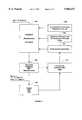
- FIG. 1shows a prior art manufacturing process
- FIGS. 2 & 3show a manufacturing process in accordance with the present invention.
- FIG. 1shows a prior art manufacturing process for the manufacture of semiconductor devices.
- a wafer lotis started as indicated at 100.
- the process parametersare set in the process equipment as indicated at 102.
- the current processis run as indicated at 104.
- the in-line critical dimensions (CD)are measured at 106.
- the wafer lotis sent to the next process at 102 where the process parameters for the next process are set in the process equipment. If the process just completed is the last process, the wafer electrical tests (WET) are conducted as indicated at 114. If, at 116, it is determined that the WET measurements are not within the WET manufacturing specifications the wafer lot is scrapped as indicated at 118. If the WET measurements are within the WET manufacturing specifications the wafer lot is sent to the next stage of the manufacturing process, which could be the dice and packaging stage as shown at 120.
- WETwafer electrical tests
- FIGS. 2 & 3a wafer manufacturing process flow in accordance with the present invention is shown.
- the wafer lotis started in the manufacturing process, as indicated at 200.
- the process parameters for the first processare set on the process equipment as indicated at 202.
- the current processis run as indicated at 204.
- the in-line critical dimensionsare measured at 206.
- the in-line critical dimensionsare input to a statistical manufacturing simulation at 300, FIG. 3.
- the statistical manufacturing simulation at 300is conducted with data from in-line critical dimension measurements from previous processes from this lot as indicated at 302.
- the statistical manufacturing simulation at 300is also conducted with data from previous lots for process steps after the current process step as indicated at 304.
- the statistical manufacturing simulation at 300also includes calibration simulation data at 306.
- the calibration simulation data at 306has input from a comparison made at 312 of the predicted WET measurements at 308 and the collected WET data from all previous process steps at 310.
- the statistical manufacturing simulation at 300determines the predicted WET measurements at 308, which are input to the decision step at 208.
- the predicted WET measurementsmay provide a widened process control window. This means, for example, that a parameter that is currently being measured may be adjusted to compensate for a parameter that has been previously measured and was either within or without that parameters specification.
- the widened process control windowprovides more flexibility to the process control engineer to continue processing a wafer lot and can result in cost savings by not having to scrap wafer lots that can be saved by merely adjusting subsequent process parameters.
- the wafer lotis scrapped if a remedy is not found, as indicated at 210. If it is determined at 208 that the predicted WET measurements are within the pre-established WET specifications, it is then determined at 212 if the current process is the last process. If the current process is not the last process, the wafer lot is sent to the next process as indicated at 214. If the current process is the last process, the WET measurements are conducted as indicated at 216. The results from the WET measurements are sent to a decision point at 218 and to a database 310 FIG. 3. The use of the WET database at 310 is discussed above. If the WET measurements are not within the WET manufacturing specification, the wafer lot is scrapped as indicated at 220. If the WET measurements are within the WET manufacturing specification, the wafer lot is sent to the next stage, as indicated at 222.
- the benefits of the present inventioninclude:
Landscapes
- Engineering & Computer Science (AREA)
- Physics & Mathematics (AREA)
- General Physics & Mathematics (AREA)
- Manufacturing & Machinery (AREA)
- Computer Hardware Design (AREA)
- Microelectronics & Electronic Packaging (AREA)
- Power Engineering (AREA)
- Testing Or Measuring Of Semiconductors Or The Like (AREA)
- General Factory Administration (AREA)
Abstract
Description
1. Cross Reference to Related Applications
This application is related to application, Ser. No. 08/985,470, filed on the filing date of this application, entitled AUTOMATIC RECIPE ADJUST AND DOWNLOAD BASED ON PROCESS CONTROL WINDOW and to the application, Ser. No. 08/985,467, filed on the filing date of this application, entitled DISPOSITION TOOL FOR FACTORY PROCESS CONTROL both of which are assigned to the assignee of this application.
2. Field of the Invention
This invention relates generally to the manufacture of high performance integrated circuits on semiconductor devices. More specifically, this invention relates to optimizing the manufacture of high performance integrated circuits on semiconductor devices. Even more specifically, this invention relates to optimizing the manufacture of high performance integrated circuits on semiconductor devices using simulated wafer electrical test data (WET) from current and previous layer data.
3. Discussion of the Related Art
In the typical semiconductor manufacturing facility, many simulation and analysis tools have been implemented to assist the process integration and device development efforts. These simulation and analysis tools, however, are typically employed to provide an indication of general trends. The latent potential of reducing the number of silicon runs and speeding up the process optimization cycle has not been fully achieved. One of the primary reasons the process optimization cycle has not been achieved is that the accuracy of the data obtained cannot be established to the degree necessary to determine the dependability of the simulation systems. The accuracy of the data obtained can only be achieved by a complete and detailed engineering calibration of the simulation system. This calibration, however, demands extensive engineering resources and data from multiple silicon production runs which, in turn, is usually only available at the latter stages of the process development or early production cycles.
In addition, process optimization for a technology that has completed qualification and is ramping-up production could receive great benefit from the extensive embedded device physics contained in advanced complex simulation tools.
Current trends in semiconductor process development include the use of these simulation tools to predict certain wafer electrical tests (WET) device performance characteristics based on a predetermined set of process values. The use of these simulation tools has been very effective. Additionally, optimal performance of current large-scale integrated devices can be predicted by a subset of critical WET performance parameters. These performance criteria include speed, operating temperature, power utilization, and reliability.
Furthermore, current manufacturing technology utilizes in-line statistical evaluation of critical parametric values at most module steps in the overall process flow. These statistical values are used to maintain control of the process, at the particular process module in question, often without regard to previous processing results. Often the goal of manufacturing is to meet not only yield goals, but certain performance goals as well. Currently, to do this it is necessary to force certain values to meet very strict specifications, such as shifting polysilicon gate critical dimensions (CD) or increasing or increasing threshold adjust implant, and hope that other process module variations will not adversely affect performance.
Therefore, what is needed is a method of achieving optimum performance is to have a tool that can provide a process control window or specification for the current module by utilizing the previous process step statistical data as a baseline that is entered into a process simulation tool. Such a process control window would have the potential of being much wider than current specifications due to the previous layer parameters and their effects being precisely known and can be considered dynamic since the process control window can change based on actual previous layer data. The simulation tool would be preset to optimize the process to hit certain critical WET parametrics. Using the previous data baseline, and knowing the WET goals, the simulator tool would then provide direction by providing a process control window for the remaining operations to achieve those goals.
A dynamic process window control using simulated WET data from current and previous layer data in accordance with the present invention provides a simulation tool that is preset to optimize the process to hit critical WET parametrics.
The above and other objects and advantages of the present invention are attained through a tool that gathers all appropriate previous layer statistical data for the lot in question and reduces it to the appropriate form for introduction to the process simulator. The tool also ascertains the WET goals for the particular lot for achieving certain performance objectives. Knowing the precondition or baseline of the lot and the projected WET goals, the simulator then provides the optimal process parametric targets for the current process module, within the widened process control limits (the wider process control window), to achieve these objectives. If it is impossible to achieve the goal, a disposition of the lot can be made including the lot being downgraded, scrapped, made inactive and a new lot can be assigned to take its place. If the target goals are not met at the current process step, the simulator will recalculate using the new data to choose the target values (process window control) for the next module step and so on until the critical process steps have all been performed.
The present invention is better understood upon consideration of the detailed description below, in conjunction with the accompanying drawings. As will become readily apparent to those skilled in the art from the following description, there is shown and described an embodiment of this invention simply by way of illustration of the best mode to carry out the invention. As will be realized, the invention is capable of other embodiments and its several details are capable of modifications in various obvious aspects, all without departing from the scope of the invention. Accordingly, the drawings and detailed description will be regarded as illustrative in nature and not as restrictive.
The novel features believed characteristic of the invention are set forth in the appended claims. The invention itself, however, as well as a preferred mode of use, and further objects and advantages thereof, will best be understood by reference to the following detailed description of an illustrative embodiment when read in conjunction with the accompanying drawings, wherein:
FIG. 1 shows a prior art manufacturing process; and
FIGS. 2 & 3 show a manufacturing process in accordance with the present invention.
Reference is now made in detail to a specific embodiment of the present invention that illustrates the best mode presently contemplated by the inventors for practicing the invention.
FIG. 1 shows a prior art manufacturing process for the manufacture of semiconductor devices. A wafer lot is started as indicated at 100. The process parameters are set in the process equipment as indicated at 102. The current process is run as indicated at 104. After the current process is completed, the in-line critical dimensions (CD) are measured at 106. At 108, it is determined if the in-line critical dimensions are within preestablished manufacturing specifications. If the in-line critical dimensions are not within the manufacturing specifications, it is attempted to find a remedy as shown at 110, and if a remedy is not available, the wafers are scrapped. If, at 108, it is determined that the in-line critical dimensions are within the manufacturing specifications, it is then determined at 112 if the process just completed is the last process. If it is not the last process, the wafer lot is sent to the next process at 102 where the process parameters for the next process are set in the process equipment. If the process just completed is the last process, the wafer electrical tests (WET) are conducted as indicated at 114. If, at 116, it is determined that the WET measurements are not within the WET manufacturing specifications the wafer lot is scrapped as indicated at 118. If the WET measurements are within the WET manufacturing specifications the wafer lot is sent to the next stage of the manufacturing process, which could be the dice and packaging stage as shown at 120.
Referring to FIGS. 2 & 3 a wafer manufacturing process flow in accordance with the present invention is shown. In FIG. 2, the wafer lot is started in the manufacturing process, as indicated at 200. The process parameters for the first process are set on the process equipment as indicated at 202. The current process is run as indicated at 204. After the current process is run, the in-line critical dimensions are measured at 206. The in-line critical dimensions are input to a statistical manufacturing simulation at 300, FIG. 3. The statistical manufacturing simulation at 300 is conducted with data from in-line critical dimension measurements from previous processes from this lot as indicated at 302. The statistical manufacturing simulation at 300 is also conducted with data from previous lots for process steps after the current process step as indicated at 304. The statistical manufacturing simulation at 300 also includes calibration simulation data at 306. The calibration simulation data at 306 has input from a comparison made at 312 of the predicted WET measurements at 308 and the collected WET data from all previous process steps at 310. The statistical manufacturing simulation at 300 determines the predicted WET measurements at 308, which are input to the decision step at 208. The predicted WET measurements may provide a widened process control window. This means, for example, that a parameter that is currently being measured may be adjusted to compensate for a parameter that has been previously measured and was either within or without that parameters specification. The widened process control window provides more flexibility to the process control engineer to continue processing a wafer lot and can result in cost savings by not having to scrap wafer lots that can be saved by merely adjusting subsequent process parameters. If it is determined at 208 that the predicted WET measurements are not within the pre-established WET specifications the wafer lot is scrapped if a remedy is not found, as indicated at 210. If it is determined at 208 that the predicted WET measurements are within the pre-established WET specifications, it is then determined at 212 if the current process is the last process. If the current process is not the last process, the wafer lot is sent to the next process as indicated at 214. If the current process is the last process, the WET measurements are conducted as indicated at 216. The results from the WET measurements are sent to a decision point at 218 and to adatabase 310 FIG. 3. The use of the WET database at 310 is discussed above. If the WET measurements are not within the WET manufacturing specification, the wafer lot is scrapped as indicated at 220. If the WET measurements are within the WET manufacturing specification, the wafer lot is sent to the next stage, as indicated at 222.
The benefits of the present invention include:
1. Allowing the specific targeting of wafer lots to achieve selected performance characteristics.
2. Allows the modification of wafer lot movement to meet production goals.
3. Provides critical information to the process engineers for disposition decisions.
4. Provides for the widening of process specification limits based on calculations from previous layer or process data.
The foregoing description of the embodiments of the invention has been presented for purposes of illustration and description. It is not intended to be exhaustive or to limit the invention to the precise form disclosed. Obvious modifications or variations are possible in light of the above teachings. The embodiment was chosen and described to provide the best illustration of the principles of the invention and its practical application to thereby enable one of ordinary skill in the art to utilize the invention in various embodiments and with various modifications as are suited to the particular use contemplated. All such modifications and variations are within the scope of the invention as determined by the appended claims when interpreted in accordance with the breadth to which they are fairly, legally, and equitably entitled.
Claims (1)
1. A method of manufacturing semiconductor wafers, the method comprising:
starting a wafer lot in a first process of a manufacturing process;
setting process parameters for the first process and running the first process;
measuring in-line critical dimensions after completion of the first process;
determining predicted wafer electrical test measurements by combining in-line critical dimensions from previous processes run on the wafer lot, data from previous lots for processes to be run subsequent to the process being run on the wafer lot and calibration simulation data obtained from a comparison of the predicted wafer electrical test measurements and collected actual wafer electrical test measurements taken from previous wafer electrical test measurements;
determining if the predicted wafer electrical test measurements are within established wafer electrical test measurement specifications; and
if the predicted wafer electrical test measurements are within the established wafer electric test measurement specifications sending the wafer lot to the next process.
Priority Applications (1)
| Application Number | Priority Date | Filing Date | Title |
|---|---|---|---|
| US08/985,566US5866437A (en) | 1997-12-05 | 1997-12-05 | Dynamic process window control using simulated wet data from current and previous layer data |
Applications Claiming Priority (1)
| Application Number | Priority Date | Filing Date | Title |
|---|---|---|---|
| US08/985,566US5866437A (en) | 1997-12-05 | 1997-12-05 | Dynamic process window control using simulated wet data from current and previous layer data |
Publications (1)
| Publication Number | Publication Date |
|---|---|
| US5866437Atrue US5866437A (en) | 1999-02-02 |
Family
ID=25531589
Family Applications (1)
| Application Number | Title | Priority Date | Filing Date |
|---|---|---|---|
| US08/985,566Expired - LifetimeUS5866437A (en) | 1997-12-05 | 1997-12-05 | Dynamic process window control using simulated wet data from current and previous layer data |
Country Status (1)
| Country | Link |
|---|---|
| US (1) | US5866437A (en) |
Cited By (48)
| Publication number | Priority date | Publication date | Assignee | Title |
|---|---|---|---|---|
| US6041270A (en)* | 1997-12-05 | 2000-03-21 | Advanced Micro Devices, Inc. | Automatic recipe adjust and download based on process control window |
| US6098024A (en)* | 1997-12-05 | 2000-08-01 | Advanced Micro Devices, Inc. | System for process data association using LaPlace Everett interpolation |
| US6154711A (en)* | 1997-12-05 | 2000-11-28 | Advanced Micro Devices, Inc. | Disposition tool for factory process control |
| US6165805A (en)* | 1998-10-29 | 2000-12-26 | Advanced Micro Devices, Inc. | Scan tool recipe server |
| WO2001011679A1 (en)* | 1999-08-10 | 2001-02-15 | Advanced Micro Devices, Inc. | Method and apparatus for performing run-to-run control in a batch manufacturing environment |
| WO2001011678A1 (en)* | 1999-08-10 | 2001-02-15 | Advanced Micro Devices, Inc. | Method and apparatus for run-to-run controlling of overlay registration |
| WO2001011680A1 (en)* | 1999-08-10 | 2001-02-15 | Advanced Micro Devices, Inc. | Method and apparatus for characterizing a semiconductor device |
| WO2001050522A1 (en)* | 2000-01-04 | 2001-07-12 | Advanced Micro Devices, Inc. | Method for determining optimal process targets in microelectronic fabrication |
| WO2001050521A1 (en)* | 2000-01-04 | 2001-07-12 | Advanced Micro Devices, Inc. | Process control system |
| US6296778B1 (en)* | 1999-03-31 | 2001-10-02 | Lam Research Corporation | Method and apparatus for simulating standard test wafers |
| US6301510B1 (en)* | 1998-03-03 | 2001-10-09 | Lam Research Corporation | Method and apparatus to calibrate a semi-empirical process simulator |
| US6300757B1 (en)* | 1998-04-21 | 2001-10-09 | Texas Instruments Deutschland, Gmbh | Procedure for the calibration of a measuring device |
| US6311096B1 (en)* | 1999-04-01 | 2001-10-30 | Texas Instruments Incorporated | Design of microelectronic process flows for manufacturability and performance |
| WO2001082365A1 (en)* | 2000-04-19 | 2001-11-01 | Advanced Micro Devices, Inc. | Method and apparatus for control of critical dimension using feedback etch control |
| WO2001080306A3 (en)* | 2000-04-13 | 2002-07-18 | Advanced Micro Devices Inc | Automated process monitoring and analysis system for semiconductor processing |
| US20020103564A1 (en)* | 2000-09-20 | 2002-08-01 | John Fielden | Methods and systems for determining a composition and a thickness of a specimen |
| US20020106848A1 (en)* | 2000-09-20 | 2002-08-08 | Dan Wack | Methods and systems for determining a property of a specimen prior to, during, or subsequent to lithography |
| US20020107650A1 (en)* | 2000-09-20 | 2002-08-08 | Dan Wack | Methods and systems for determining a critical dimension and a presence of defects on a specimen |
| WO2002031613A3 (en)* | 2000-10-13 | 2002-10-17 | Insyst Ltd | System and method for monitoring process quality control |
| EP1271246A1 (en)* | 2001-06-19 | 2003-01-02 | Infineon Technologies AG | Method for monitoring the quality of a lithographic structuring step |
| US6532428B1 (en)* | 1999-10-07 | 2003-03-11 | Advanced Micro Devices, Inc. | Method and apparatus for automatic calibration of critical dimension metrology tool |
| US6556882B1 (en)* | 1999-09-22 | 2003-04-29 | Advanced Micro Devices, Inc. | Method and apparatus for generating real-time data from static files |
| US6594598B1 (en)* | 1997-10-08 | 2003-07-15 | Matsushita Electronics Corporation | Method for controlling production line |
| WO2002101793A3 (en)* | 2001-06-12 | 2003-11-13 | Applied Materials Inc | Systems and methods for calibrating integrated inspection tools |
| US6673637B2 (en) | 2000-09-20 | 2004-01-06 | Kla-Tencor Technologies | Methods and systems for determining a presence of macro defects and overlay of a specimen |
| US20040007325A1 (en)* | 2002-06-11 | 2004-01-15 | Applied Materials, Inc. | Integrated equipment set for forming a low K dielectric interconnect on a substrate |
| US6694284B1 (en) | 2000-09-20 | 2004-02-17 | Kla-Tencor Technologies Corp. | Methods and systems for determining at least four properties of a specimen |
| US6732007B1 (en)* | 2002-06-05 | 2004-05-04 | Advanced Micro Devices, Inc. | Method and apparatus for implementing dynamic qualification recipes |
| US20040088068A1 (en)* | 2002-10-31 | 2004-05-06 | Daniel Kadosh | Method and apparatus for providing first-principles feed-forward manufacturing control |
| US20040206621A1 (en)* | 2002-06-11 | 2004-10-21 | Hongwen Li | Integrated equipment set for forming a low K dielectric interconnect on a substrate |
| US6812045B1 (en) | 2000-09-20 | 2004-11-02 | Kla-Tencor, Inc. | Methods and systems for determining a characteristic of a specimen prior to, during, or subsequent to ion implantation |
| US20040235205A1 (en)* | 2000-09-20 | 2004-11-25 | Kla-Tencor, Inc. | Methods and systems for determining a critical dimension and overlay of a specimen |
| US6863536B1 (en) | 1998-01-26 | 2005-03-08 | Simbionix Ltd. | Endoscopic tutorial system with a bleeding complication |
| US20050071036A1 (en)* | 2003-09-30 | 2005-03-31 | Tokyo Electron Limited | System and method for using first-principles simulation to characterize a semiconductor manufacturing process |
| US20050071037A1 (en)* | 2003-09-30 | 2005-03-31 | Tokyo Electron Limited | System and method for using first-principles simulation to analyze a process performed by a semiconductor processing tool |
| US20050071035A1 (en)* | 2003-09-30 | 2005-03-31 | Tokyo Electron Limited | System and method for using first-principles simulation to control a semiconductor manufacturing process |
| US20050071034A1 (en)* | 2003-09-30 | 2005-03-31 | Tokyo Electron Limited | System and method for using first-principles simulation to facilitate a semiconductor manufacturing process |
| US20050071038A1 (en)* | 2003-09-30 | 2005-03-31 | Tokyo Electron Limited | System and method for using first-principles simulation to control a semiconductor manufacturing process |
| US20050136560A1 (en)* | 2003-12-19 | 2005-06-23 | Intel Corporation | Process control apparatus, systems, and methods |
| US6919957B2 (en) | 2000-09-20 | 2005-07-19 | Kla-Tencor Technologies Corp. | Methods and systems for determining a critical dimension, a presence of defects, and a thin film characteristic of a specimen |
| US7106425B1 (en) | 2000-09-20 | 2006-09-12 | Kla-Tencor Technologies Corp. | Methods and systems for determining a presence of defects and a thin film characteristic of a specimen |
| US7130029B2 (en) | 2000-09-20 | 2006-10-31 | Kla-Tencor Technologies Corp. | Methods and systems for determining an adhesion characteristic and a thickness of a specimen |
| DE102006004411A1 (en)* | 2006-01-31 | 2007-08-02 | Advanced Micro Devices, Inc., Sunnyvale | Evaluation method for assessing measurement data during the processing of semiconductors uses data filtering based on correlation |
| US20080195857A1 (en)* | 2007-02-09 | 2008-08-14 | Sony Corporation | Techniques For Automatic Registration Of Appliances |
| US20090284722A1 (en)* | 2008-05-19 | 2009-11-19 | International Business Machines Corporation | Method for monitoring focus on an integrated wafer |
| CN102955363A (en)* | 2011-08-19 | 2013-03-06 | 上海华虹Nec电子有限公司 | Optical proximity correction online monitoring method |
| US10310490B2 (en) | 2016-02-01 | 2019-06-04 | Qoniac Gmbh | Method and apparatus of evaluating a semiconductor manufacturing process |
| CN110622069A (en)* | 2017-05-05 | 2019-12-27 | Asml荷兰有限公司 | Method for predicting yield of device manufacturing process |
Citations (3)
| Publication number | Priority date | Publication date | Assignee | Title |
|---|---|---|---|---|
| US5637186A (en)* | 1995-11-22 | 1997-06-10 | United Microelectronics Corporation | Method and monitor testsite pattern for measuring critical dimension openings |
| US5663076A (en)* | 1995-08-08 | 1997-09-02 | Lsi Logic Corporation | Automating photolithography in the fabrication of integrated circuits |
| US5716856A (en)* | 1995-08-22 | 1998-02-10 | Advanced Micro Devices, Inc. | Arrangement and method for detecting sequential processing effects in manufacturing using predetermined sequences within runs |
- 1997
- 1997-12-05USUS08/985,566patent/US5866437A/ennot_activeExpired - Lifetime
Patent Citations (3)
| Publication number | Priority date | Publication date | Assignee | Title |
|---|---|---|---|---|
| US5663076A (en)* | 1995-08-08 | 1997-09-02 | Lsi Logic Corporation | Automating photolithography in the fabrication of integrated circuits |
| US5716856A (en)* | 1995-08-22 | 1998-02-10 | Advanced Micro Devices, Inc. | Arrangement and method for detecting sequential processing effects in manufacturing using predetermined sequences within runs |
| US5637186A (en)* | 1995-11-22 | 1997-06-10 | United Microelectronics Corporation | Method and monitor testsite pattern for measuring critical dimension openings |
Cited By (107)
| Publication number | Priority date | Publication date | Assignee | Title |
|---|---|---|---|---|
| US6594598B1 (en)* | 1997-10-08 | 2003-07-15 | Matsushita Electronics Corporation | Method for controlling production line |
| US6098024A (en)* | 1997-12-05 | 2000-08-01 | Advanced Micro Devices, Inc. | System for process data association using LaPlace Everett interpolation |
| US6154711A (en)* | 1997-12-05 | 2000-11-28 | Advanced Micro Devices, Inc. | Disposition tool for factory process control |
| US6041270A (en)* | 1997-12-05 | 2000-03-21 | Advanced Micro Devices, Inc. | Automatic recipe adjust and download based on process control window |
| US6863536B1 (en) | 1998-01-26 | 2005-03-08 | Simbionix Ltd. | Endoscopic tutorial system with a bleeding complication |
| US6301510B1 (en)* | 1998-03-03 | 2001-10-09 | Lam Research Corporation | Method and apparatus to calibrate a semi-empirical process simulator |
| USRE39534E1 (en)* | 1998-03-03 | 2007-03-27 | Lam Research Corporation | Method and apparatus to calibrate a semi-empirical process simulator |
| US20050278057A1 (en)* | 1998-03-03 | 2005-12-15 | David Cooperberg | Enhanced process and profile simulator algorithms |
| US7139632B2 (en) | 1998-03-03 | 2006-11-21 | Lam Research Corporation | Enhanced process and profile simulator algorithms |
| US6300757B1 (en)* | 1998-04-21 | 2001-10-09 | Texas Instruments Deutschland, Gmbh | Procedure for the calibration of a measuring device |
| US6165805A (en)* | 1998-10-29 | 2000-12-26 | Advanced Micro Devices, Inc. | Scan tool recipe server |
| US6296778B1 (en)* | 1999-03-31 | 2001-10-02 | Lam Research Corporation | Method and apparatus for simulating standard test wafers |
| US6311096B1 (en)* | 1999-04-01 | 2001-10-30 | Texas Instruments Incorporated | Design of microelectronic process flows for manufacturability and performance |
| US6319737B1 (en) | 1999-08-10 | 2001-11-20 | Advanced Micro Devices, Inc. | Method and apparatus for characterizing a semiconductor device |
| WO2001011680A1 (en)* | 1999-08-10 | 2001-02-15 | Advanced Micro Devices, Inc. | Method and apparatus for characterizing a semiconductor device |
| US6405096B1 (en) | 1999-08-10 | 2002-06-11 | Advanced Micro Devices, Inc. | Method and apparatus for run-to-run controlling of overlay registration |
| WO2001011679A1 (en)* | 1999-08-10 | 2001-02-15 | Advanced Micro Devices, Inc. | Method and apparatus for performing run-to-run control in a batch manufacturing environment |
| US6607926B1 (en) | 1999-08-10 | 2003-08-19 | Advanced Micro Devices, Inc. | Method and apparatus for performing run-to-run control in a batch manufacturing environment |
| WO2001011678A1 (en)* | 1999-08-10 | 2001-02-15 | Advanced Micro Devices, Inc. | Method and apparatus for run-to-run controlling of overlay registration |
| US6556882B1 (en)* | 1999-09-22 | 2003-04-29 | Advanced Micro Devices, Inc. | Method and apparatus for generating real-time data from static files |
| US6532428B1 (en)* | 1999-10-07 | 2003-03-11 | Advanced Micro Devices, Inc. | Method and apparatus for automatic calibration of critical dimension metrology tool |
| US6449524B1 (en) | 2000-01-04 | 2002-09-10 | Advanced Micro Devices, Inc. | Method and apparatus for using equipment state data for run-to-run control of manufacturing tools |
| US6470230B1 (en) | 2000-01-04 | 2002-10-22 | Advanced Micro Devices, Inc. | Supervisory method for determining optimal process targets based on product performance in microelectronic fabrication |
| WO2001050522A1 (en)* | 2000-01-04 | 2001-07-12 | Advanced Micro Devices, Inc. | Method for determining optimal process targets in microelectronic fabrication |
| WO2001050521A1 (en)* | 2000-01-04 | 2001-07-12 | Advanced Micro Devices, Inc. | Process control system |
| US6622059B1 (en)* | 2000-04-13 | 2003-09-16 | Advanced Micro Devices, Inc. | Automated process monitoring and analysis system for semiconductor processing |
| WO2001080306A3 (en)* | 2000-04-13 | 2002-07-18 | Advanced Micro Devices Inc | Automated process monitoring and analysis system for semiconductor processing |
| WO2001082365A1 (en)* | 2000-04-19 | 2001-11-01 | Advanced Micro Devices, Inc. | Method and apparatus for control of critical dimension using feedback etch control |
| US20040235205A1 (en)* | 2000-09-20 | 2004-11-25 | Kla-Tencor, Inc. | Methods and systems for determining a critical dimension and overlay of a specimen |
| US6950196B2 (en) | 2000-09-20 | 2005-09-27 | Kla-Tencor Technologies Corp. | Methods and systems for determining a thickness of a structure on a specimen and at least one additional property of the specimen |
| US8502979B2 (en) | 2000-09-20 | 2013-08-06 | Kla-Tencor Technologies Corp. | Methods and systems for determining a critical dimension and overlay of a specimen |
| US20020190207A1 (en)* | 2000-09-20 | 2002-12-19 | Ady Levy | Methods and systems for determining a characteristic of micro defects on a specimen |
| US20020179867A1 (en)* | 2000-09-20 | 2002-12-05 | John Fielden | Methods and systems for determining flatness, a presence of defects, and a thin film characteristic of a specimen |
| US6633831B2 (en) | 2000-09-20 | 2003-10-14 | Kla Tencor Technologies | Methods and systems for determining a critical dimension and a thin film characteristic of a specimen |
| US8179530B2 (en) | 2000-09-20 | 2012-05-15 | Kla-Tencor Technologies Corp. | Methods and systems for determining a critical dimension and overlay of a specimen |
| US7751046B2 (en) | 2000-09-20 | 2010-07-06 | Kla-Tencor Technologies Corp. | Methods and systems for determining a critical dimension and overlay of a specimen |
| US6673637B2 (en) | 2000-09-20 | 2004-01-06 | Kla-Tencor Technologies | Methods and systems for determining a presence of macro defects and overlay of a specimen |
| US7460981B2 (en) | 2000-09-20 | 2008-12-02 | Kla-Tencor Technologies Corp. | Methods and systems for determining a presence of macro and micro defects on a specimen |
| US6694284B1 (en) | 2000-09-20 | 2004-02-17 | Kla-Tencor Technologies Corp. | Methods and systems for determining at least four properties of a specimen |
| US20040073398A1 (en)* | 2000-09-20 | 2004-04-15 | Kla-Tencor, Inc. | Methods and systems for determining a critical dimension and a thin film characteristic of a specimen |
| US7349090B2 (en) | 2000-09-20 | 2008-03-25 | Kla-Tencor Technologies Corp. | Methods and systems for determining a property of a specimen prior to, during, or subsequent to lithography |
| US20020103564A1 (en)* | 2000-09-20 | 2002-08-01 | John Fielden | Methods and systems for determining a composition and a thickness of a specimen |
| US20040092045A1 (en)* | 2000-09-20 | 2004-05-13 | Gary Bultman | Methods and systems for determining a presence of macro and micro defects on a specimen |
| US20040115843A1 (en)* | 2000-09-20 | 2004-06-17 | Kla-Tencor, Inc. | Methods and systems for determining a presence of macro defects and overlay of a specimen |
| US7196782B2 (en) | 2000-09-20 | 2007-03-27 | Kla-Tencor Technologies Corp. | Methods and systems for determining a thin film characteristic and an electrical property of a specimen |
| US7139083B2 (en) | 2000-09-20 | 2006-11-21 | Kla-Tencor Technologies Corp. | Methods and systems for determining a composition and a thickness of a specimen |
| US6782337B2 (en) | 2000-09-20 | 2004-08-24 | Kla-Tencor Technologies Corp. | Methods and systems for determining a critical dimension an a presence of defects on a specimen |
| US6806951B2 (en) | 2000-09-20 | 2004-10-19 | Kla-Tencor Technologies Corp. | Methods and systems for determining at least one characteristic of defects on at least two sides of a specimen |
| US20020106848A1 (en)* | 2000-09-20 | 2002-08-08 | Dan Wack | Methods and systems for determining a property of a specimen prior to, during, or subsequent to lithography |
| US6812045B1 (en) | 2000-09-20 | 2004-11-02 | Kla-Tencor, Inc. | Methods and systems for determining a characteristic of a specimen prior to, during, or subsequent to ion implantation |
| US6818459B2 (en) | 2000-09-20 | 2004-11-16 | Kla-Tencor Technologies Corp. | Methods and systems for determining a presence of macro defects and overlay of a specimen |
| US20020179864A1 (en)* | 2000-09-20 | 2002-12-05 | John Fielden | Methods and systems for determining a thin film characteristic and an electrical property of a specimen |
| US6829559B2 (en) | 2000-09-20 | 2004-12-07 | K.L.A.-Tencor Technologies | Methods and systems for determining a presence of macro and micro defects on a specimen |
| US7130029B2 (en) | 2000-09-20 | 2006-10-31 | Kla-Tencor Technologies Corp. | Methods and systems for determining an adhesion characteristic and a thickness of a specimen |
| US7106425B1 (en) | 2000-09-20 | 2006-09-12 | Kla-Tencor Technologies Corp. | Methods and systems for determining a presence of defects and a thin film characteristic of a specimen |
| US20060072807A1 (en)* | 2000-09-20 | 2006-04-06 | Kla-Tencor Technologies. | Methods and systems for determining a presence of macro and micro defects on a specimen |
| US7006235B2 (en) | 2000-09-20 | 2006-02-28 | Kla-Tencor Technologies Corp. | Methods and systems for determining overlay and flatness of a specimen |
| US20020107650A1 (en)* | 2000-09-20 | 2002-08-08 | Dan Wack | Methods and systems for determining a critical dimension and a presence of defects on a specimen |
| US20030011786A1 (en)* | 2000-09-20 | 2003-01-16 | Ady Levy | Methods and systems for determining overlay and flatness of a specimen |
| US6946394B2 (en) | 2000-09-20 | 2005-09-20 | Kla-Tencor Technologies | Methods and systems for determining a characteristic of a layer formed on a specimen by a deposition process |
| US6891610B2 (en) | 2000-09-20 | 2005-05-10 | Kla-Tencor Technologies Corp. | Methods and systems for determining an implant characteristic and a presence of defects on a specimen |
| US6891627B1 (en) | 2000-09-20 | 2005-05-10 | Kla-Tencor Technologies Corp. | Methods and systems for determining a critical dimension and overlay of a specimen |
| US6919957B2 (en) | 2000-09-20 | 2005-07-19 | Kla-Tencor Technologies Corp. | Methods and systems for determining a critical dimension, a presence of defects, and a thin film characteristic of a specimen |
| US6917419B2 (en) | 2000-09-20 | 2005-07-12 | Kla-Tencor Technologies Corp. | Methods and systems for determining flatness, a presence of defects, and a thin film characteristic of a specimen |
| US6917433B2 (en) | 2000-09-20 | 2005-07-12 | Kla-Tencor Technologies Corp. | Methods and systems for determining a property of a specimen prior to, during, or subsequent to an etch process |
| WO2002031613A3 (en)* | 2000-10-13 | 2002-10-17 | Insyst Ltd | System and method for monitoring process quality control |
| WO2002101793A3 (en)* | 2001-06-12 | 2003-11-13 | Applied Materials Inc | Systems and methods for calibrating integrated inspection tools |
| US6654698B2 (en) | 2001-06-12 | 2003-11-25 | Applied Materials, Inc. | Systems and methods for calibrating integrated inspection tools |
| EP1271246A1 (en)* | 2001-06-19 | 2003-01-02 | Infineon Technologies AG | Method for monitoring the quality of a lithographic structuring step |
| US6780552B2 (en) | 2001-06-19 | 2004-08-24 | Infineon Technologies Ag | Method for controlling the quality of a lithographic structuring step |
| US6732007B1 (en)* | 2002-06-05 | 2004-05-04 | Advanced Micro Devices, Inc. | Method and apparatus for implementing dynamic qualification recipes |
| US20040206621A1 (en)* | 2002-06-11 | 2004-10-21 | Hongwen Li | Integrated equipment set for forming a low K dielectric interconnect on a substrate |
| US20040007325A1 (en)* | 2002-06-11 | 2004-01-15 | Applied Materials, Inc. | Integrated equipment set for forming a low K dielectric interconnect on a substrate |
| US20060246683A1 (en)* | 2002-06-11 | 2006-11-02 | Applied Materials, Inc. | Integrated equipment set for forming a low K dielectric interconnect on a substrate |
| WO2004040624A3 (en)* | 2002-10-31 | 2004-07-01 | Advanced Micro Devices Inc | Method and apparatus for controlling a manufacturing process |
| US20040088068A1 (en)* | 2002-10-31 | 2004-05-06 | Daniel Kadosh | Method and apparatus for providing first-principles feed-forward manufacturing control |
| US20050071039A1 (en)* | 2003-09-30 | 2005-03-31 | Tokyo Electron Limited | System and method for using first-principles simulation to provide virtual sensors that facilitate a semiconductor manufacturing process |
| US20050071034A1 (en)* | 2003-09-30 | 2005-03-31 | Tokyo Electron Limited | System and method for using first-principles simulation to facilitate a semiconductor manufacturing process |
| US8036869B2 (en) | 2003-09-30 | 2011-10-11 | Tokyo Electron Limited | System and method for using first-principles simulation to control a semiconductor manufacturing process via a simulation result or a derived empirical model |
| US20050071038A1 (en)* | 2003-09-30 | 2005-03-31 | Tokyo Electron Limited | System and method for using first-principles simulation to control a semiconductor manufacturing process |
| US20050071036A1 (en)* | 2003-09-30 | 2005-03-31 | Tokyo Electron Limited | System and method for using first-principles simulation to characterize a semiconductor manufacturing process |
| US8032348B2 (en)* | 2003-09-30 | 2011-10-04 | Tokyo Electron Limited | System and method for using first-principles simulation to facilitate a semiconductor manufacturing process |
| US8296687B2 (en) | 2003-09-30 | 2012-10-23 | Tokyo Electron Limited | System and method for using first-principles simulation to analyze a process performed by a semiconductor processing tool |
| US8050900B2 (en)* | 2003-09-30 | 2011-11-01 | Tokyo Electron Limited | System and method for using first-principles simulation to provide virtual sensors that facilitate a semiconductor manufacturing process |
| US20050071037A1 (en)* | 2003-09-30 | 2005-03-31 | Tokyo Electron Limited | System and method for using first-principles simulation to analyze a process performed by a semiconductor processing tool |
| US8073667B2 (en)* | 2003-09-30 | 2011-12-06 | Tokyo Electron Limited | System and method for using first-principles simulation to control a semiconductor manufacturing process |
| US20050071035A1 (en)* | 2003-09-30 | 2005-03-31 | Tokyo Electron Limited | System and method for using first-principles simulation to control a semiconductor manufacturing process |
| US8014991B2 (en)* | 2003-09-30 | 2011-09-06 | Tokyo Electron Limited | System and method for using first-principles simulation to characterize a semiconductor manufacturing process |
| US6999848B2 (en)* | 2003-12-19 | 2006-02-14 | Intel Corporation | Process control apparatus, systems, and methods |
| US20050136560A1 (en)* | 2003-12-19 | 2005-06-23 | Intel Corporation | Process control apparatus, systems, and methods |
| US20070177135A1 (en)* | 2006-01-31 | 2007-08-02 | Garry Tuohy | Method and system for measurement data evaluation in semiconductor processing by correlation-based data filtering |
| US7421358B2 (en) | 2006-01-31 | 2008-09-02 | Advanced Micro Devices, Inc. | Method and system for measurement data evaluation in semiconductor processing by correlation-based data filtering |
| DE102006004411A1 (en)* | 2006-01-31 | 2007-08-02 | Advanced Micro Devices, Inc., Sunnyvale | Evaluation method for assessing measurement data during the processing of semiconductors uses data filtering based on correlation |
| DE102006004411B4 (en)* | 2006-01-31 | 2017-11-09 | Globalfoundries Inc. | Method and system for measuring data evaluation in semiconductor processing by correlation-based data filtering |
| US20080195857A1 (en)* | 2007-02-09 | 2008-08-14 | Sony Corporation | Techniques For Automatic Registration Of Appliances |
| US20090284722A1 (en)* | 2008-05-19 | 2009-11-19 | International Business Machines Corporation | Method for monitoring focus on an integrated wafer |
| US9046788B2 (en)* | 2008-05-19 | 2015-06-02 | International Business Machines Corporation | Method for monitoring focus on an integrated wafer |
| CN102955363A (en)* | 2011-08-19 | 2013-03-06 | 上海华虹Nec电子有限公司 | Optical proximity correction online monitoring method |
| CN102955363B (en)* | 2011-08-19 | 2014-10-08 | 上海华虹宏力半导体制造有限公司 | Optical proximity correction online monitoring method |
| US10310490B2 (en) | 2016-02-01 | 2019-06-04 | Qoniac Gmbh | Method and apparatus of evaluating a semiconductor manufacturing process |
| CN110622069A (en)* | 2017-05-05 | 2019-12-27 | Asml荷兰有限公司 | Method for predicting yield of device manufacturing process |
| US20200103761A1 (en)* | 2017-05-05 | 2020-04-02 | Asml Netherlands B.V. | Method to predict yield of a device manufacturing process |
| US11086229B2 (en)* | 2017-05-05 | 2021-08-10 | Asml Netherlands B.V. | Method to predict yield of a device manufacturing process |
| CN110622069B (en)* | 2017-05-05 | 2022-08-09 | Asml荷兰有限公司 | Method for predicting the yield of a device manufacturing process |
| CN115220311A (en)* | 2017-05-05 | 2022-10-21 | Asml荷兰有限公司 | Method for predicting yield of device manufacturing process |
| TWI800704B (en)* | 2017-05-05 | 2023-05-01 | 荷蘭商Asml荷蘭公司 | Method to predict yield of a device manufacturing process |
| US11714357B2 (en) | 2017-05-05 | 2023-08-01 | Asml Netherlands B.V. | Method to predict yield of a device manufacturing process |
Similar Documents
| Publication | Publication Date | Title |
|---|---|---|
| US5866437A (en) | Dynamic process window control using simulated wet data from current and previous layer data | |
| US6041270A (en) | Automatic recipe adjust and download based on process control window | |
| US6154711A (en) | Disposition tool for factory process control | |
| Cory et al. | Speed binning with path delay test in 150-nm technology | |
| CN103247518B (en) | Improve the new design of the instrumental function of the FAB technique in semiconductor manufacture | |
| US6061814A (en) | Test circuitry for determining the defect density of a semiconductor process as a function of individual metal layers | |
| US7626852B2 (en) | Adaptive voltage control for SRAM | |
| US8380478B2 (en) | Statistical evaluation of circuit robustness separating local and global variation | |
| US8108060B2 (en) | System and method for implementing a wafer acceptance test (“WAT”) advanced process control (“APC”) with novel sampling policy and architecture | |
| US6757873B2 (en) | Simulator of semiconductor device circuit characteristic and simulation method | |
| US7542880B2 (en) | Time weighted moving average filter | |
| Kim et al. | Modeling manufacturing yield and reliability | |
| US6487701B1 (en) | System and method for AC performance tuning by thereshold voltage shifting in tubbed semiconductor technology | |
| US6784001B2 (en) | Automated variation of stepper exposure dose based upon across wafer variations in device characteristics, and system for accomplishing same | |
| CN102854848B (en) | Data representation relating to a non-sampled workpiece | |
| US6098024A (en) | System for process data association using LaPlace Everett interpolation | |
| US9514999B2 (en) | Systems and methods for semiconductor line scribe line centering | |
| US9262569B2 (en) | Balancing sensitivities with respect to timing closure for integrated circuits | |
| CN100362358C (en) | Scattering Measurement Method of Ring Oscillator | |
| JPH11260931A (en) | Method of estimating market failure rate of semiconductor integrated circuit device, method of manufacturing semiconductor integrated circuit device, and semiconductor integrated circuit device for test | |
| US5252508A (en) | Apparatus and method for the fabrication of semiconductor circuits | |
| US7236840B2 (en) | Manufacturing process developing method for semiconductor device | |
| CN1982907A (en) | Method for testing transistor life | |
| TWI871198B (en) | Chip test system and method | |
| Boskin et al. | IC performance prediction from electrical test measurements |
Legal Events
| Date | Code | Title | Description |
|---|---|---|---|
| AS | Assignment | Owner name:ADVANCED MICRO DEVICES, INC., CALIFORNIA Free format text:ASSIGNMENT OF ASSIGNORS INTEREST;ASSIGNORS:CHEN, MING CHUN;STEFFAN, PAUL J.;REEL/FRAME:008884/0131 Effective date:19971203 | |
| STCF | Information on status: patent grant | Free format text:PATENTED CASE | |
| FPAY | Fee payment | Year of fee payment:4 | |
| FPAY | Fee payment | Year of fee payment:8 | |
| AS | Assignment | Owner name:GLOBALFOUNDRIES INC., CAYMAN ISLANDS Free format text:AFFIRMATION OF PATENT ASSIGNMENT;ASSIGNOR:ADVANCED MICRO DEVICES, INC.;REEL/FRAME:023119/0083 Effective date:20090630 | |
| FPAY | Fee payment | Year of fee payment:12 | |
| AS | Assignment | Owner name:GLOBALFOUNDRIES U.S. INC., NEW YORK Free format text:RELEASE BY SECURED PARTY;ASSIGNOR:WILMINGTON TRUST, NATIONAL ASSOCIATION;REEL/FRAME:056987/0001 Effective date:20201117 |