US5864592A - Timing recovery system for digital subscriber line transceivers - Google Patents
Timing recovery system for digital subscriber line transceiversDownload PDFInfo
- Publication number
- US5864592A US5864592AUS07/970,816US97081692AUS5864592AUS 5864592 AUS5864592 AUS 5864592AUS 97081692 AUS97081692 AUS 97081692AUS 5864592 AUS5864592 AUS 5864592A
- Authority
- US
- United States
- Prior art keywords
- transceiver
- phase
- phase error
- receiver
- transceivers
- Prior art date
- Legal status (The legal status is an assumption and is not a legal conclusion. Google has not performed a legal analysis and makes no representation as to the accuracy of the status listed.)
- Expired - Lifetime
Links
Images


Classifications
- H—ELECTRICITY
- H04—ELECTRIC COMMUNICATION TECHNIQUE
- H04J—MULTIPLEX COMMUNICATION
- H04J3/00—Time-division multiplex systems
- H04J3/02—Details
- H04J3/06—Synchronising arrangements
- H04J3/0635—Clock or time synchronisation in a network
- H04J3/0676—Mutual
- H—ELECTRICITY
- H04—ELECTRIC COMMUNICATION TECHNIQUE
- H04L—TRANSMISSION OF DIGITAL INFORMATION, e.g. TELEGRAPHIC COMMUNICATION
- H04L7/00—Arrangements for synchronising receiver with transmitter
Definitions
- This inventionrelates generally to digital subscriber line data transmission systems and more particularly to an improved timing recovery system for use therein.
- Modern subscriber line transceiverstypically use digitally implemented signal processing hardware which requires expensive high resolution analog-to-digital converters (ADC's) having a large dynamic range.
- ADCanalog-to-digital converters
- a single high bit-rate data streamis often split into multiple lower rate streams and each such stream is transmitted down a separate twisted pair channel and combined at the far end to reconstruct the original signal.
- HDSLHigh Bit-Rate Digital Subscriber Line
- a 1.544 Mbit/sec T-1 data streamis transmitted over two channels each operating at a rate of 784 Kbit/sec (772 Kbit/sec of T-1 data plus 12 Kbit/sec of overhead).
- two transceiversare normally required at each end of the subscriber loop thereby implying a need for four high resolution ADC's per subscriber.
- transceiversare located at the central office (CO) and at a remote terminal (RT) in the subscriber premises.
- the master timing source for such a systemis supplied by the central office and the RT transceivers derive their timing information from the received signal.
- the RT transceiversare slaved to the CO transceiver's timing reference.
- Timing recovery in the RT transceiversis typically performed by phase-locked loops which generate a local clock whose frequency is identical to the frequency of the transmitter's clock in the CO transceiver.
- phase-locked loopswhich generate a local clock whose frequency is identical to the frequency of the transmitter's clock in the CO transceiver.
- Time sharing a single high sample rate ADC to digitize multiple analog signalsis commonly used in instrumentation systems having large dynamic range requirements.
- N signalsare to be digitized at a sampling rate of F S samples/sec, then these N signals are multiplexed into a single ADC operating at a sampling rate of NF S samples/sec
- the effective sampling rate of each analog signalis F S
- there is a phase offset of d1/NF S seconds between the samples in each channel.
- the present inventionis directed to an improved timing recovery system which enables two or more receivers at one end of a digital subscriber loop to share a single ADC while still allowing optimal phasing of each receiver clock relative to its received signal.
- the respective receiver clocks generated at one end of the subscriber loopare phase offset by a fixed amount.
- the receiver clocks respectively used by the N receivers at the loop remote endwould be offset by 360°/N.
- optimal phasingis nevertheless achieved by controlling at least one of the transmitter clocks at the other end (i.e., central office (CO) end) of the subscriber loop to vary the phase of the signal transmitted therefrom.
- COcentral office
- a receiver's clock recovery phase-locked loopsends back control information to the other end of the subscriber loop to phase adjust a transmitter clock.
- the transmitted signalcan be optimally phased relative to a fixed receiver clock.
- the two receivers at one end of a subscriber loopcan timeshare a single ADC operating at twice the nominal sampling rate.
- This single ADCsamples the received signals on the two channels with a fixed 180° offset between the two sampling phases.
- the individual receiversare still both able to achieve optimal performance because of the system's ability to optimally phase the transmitted signal relative to a fixed receiver clock.
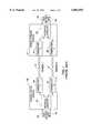
- FIG. 1is a block diagram depicting a prior art data transmission system operating over two twisted pair channels
- FIG. 2is a block diagram depicting a prior art digital full-duplex transceiver incorporating an analog-to-digital (ADC) converter at the front end of the receiver;
- ADCanalog-to-digital
- FIG. 3is a block diagram depicting a typical prior art HDSL system in which the transmitter clocks are fixed and the receiver clocks are phase adjusted to optimize signal detection;
- FIG. 4Ais a block diagram depicting a prior art clock recovery means typically used in a phase-locked loop at the remote (RT) end of a subscriber loop;
- FIG. 4Bis a block diagram depicting a prior art clock recovery means typically used in a phase-locked loop at the central office (CO) end of a subscriber loop;
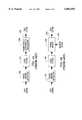
- FIG. 5is a block diagram depicting a system in accordance with the invention wherein the receiver clocks are fixed in phase relative to one another and the transmitter clock phases are adjusted to optimize signal detection;
- FIG. 6is a block diagram depicting transmission and reception of phase error commands for adjusting transmitter clock phases in accordance with the invention.
- FIG. 7is a block diagram depicting how a single ADC is timeshared by two receivers in accordance with the present invention.
- FIG. 8is a timing diagram applicable to FIG. 7.
- FIG. 1comprises a block diagram of a typical prior art data full duplex transmission system for communicating data from a central office station 12 to a remote terminal station 14 via multiple loops or channels 16, 18.
- the channelscan be implemented in many different forms, it will be assumed herein that they comprise twisted wire pairs, unless otherwise stated.
- the central office station 12includes first and second transceivers 20, 22 respectively connected to first ends of the channel media 16, 18.
- the remote terminal station 14similarly includes third and fourth transceivers 24, 26 respectively connected to second ends of the channel media 16, 18.
- transceivers 20, 22are connected to interface circuitry 30 which bidirectionally transfers high bit rate data streams 32, 34 to local equipment (not shown).
- transceivers 24, 26 of remote terminal station 14are connected to interface circuitry 36 which sends and receives high bit rate data streams 38, 40.
- FIG. 2depicts a typical prior art transceiver which can be readily utilized in the system of FIG. 1.
- the transceiver of FIG. 2is basically comprised of a transmitter 50, a receiver 52, an analog to digital converter (ADC) 54, and an echo canceler 56.
- ADCanalog to digital converter
- FIG. 2further shows a conventional hybrid circuit 60 for coupling the transmitter 50 and ADC 54 to the twisted wire pair, e.g. 16.
- Data to be transmitted over the twisted wire pair 16 from transmitter 50is supplied via input line 64 to both transmitter 50 and echo canceler 56.
- the transmitter 50 timingis controlled by an applied transmit clock (XMT CLK) signal 66 which establishes the relative phase of the transmitted signal.
- the echo canceler 56functions in a well known manner to remove the echo of a transmitted signal from a received signal. More particularly, the output of the echo canceler 56 is applied via terminal 68 to a subtractive input of a summer 70.
- the output of the ADC 54is supplied via terminal 72 to the additive input of summer 70.
- the output of summer 70is applied via line 72 to the receiver 52 which produces the received data output signal on line 74.
- the receiver 52 and ADC 54are supplied with a receive clock timing signal (RCV CLK) on terminal 78 produced by clock recovery circuitry comprising phase control circuit 80 responsive to an output 82 of receiver 52.
- the phase control circuit 80is connected in a phase lock loop and responds to a phase error detected on receiver output 82 to vary the phase of the RCV CLK to minimize the phase error.
- the use of phase lock loops employing phase control circuits 80 as depicted in FIG. 2are well known in the data communications art for timing recovery.
- FIG. 3depicts the data transmission system of FIG. 1 in greater detail showing how phase lock loops are typically employed in conjunction with each transceiver receiver to generate an optimally phased receive clock signal (RCV CLK). More particularly, note in FIG. 3 that a central office master clock source 90 supplies a master clock signal to the phase control circuits 92, 94 associated with the first and second transceivers 20, 22. The circuits 92, 94 respectively produce RCV CLK 1 and RCV CLK 2.
- FIG. 4Billustrates a block diagram of a typical central office phase control circuit, i.e. 92 or 94.
- the phase control circuit of FIG. 4Bis comprised of a phase error detector 96 which has as its input a receive signal from its associated receiver.
- the output of the phase error detector 96is applied to a loop filter 98 whose output is coupled to a phase adjust circuit 100.
- the master clock from source 90is applied as an input 102 to the phase adjust circuit 100.
- the circuit 100then produces a receive clock signal (RCV CLK) on output 104, whose phase can vary from that of the master clock 102, depending upon the phase error indicated by the receive signal applied to the detector.
- RCV CLKreceive clock signal
- the remote terminal transceivers 24, 26respectively have phase control circuits 108, 110 connected to their receivers (FIG. 3).
- the function of the phase control circuits 108, 110is to recover an optimally phased receive clock (RCV CLK) from the signals received respectively at the second ends of channels 1 and 2.
- FIG. 4AAn exemplary block diagram of the phase control circuits 108, 110 is depicted in FIG. 4A.
- This remote terminal phase control circuitis comprised of a phase error detector 116 whose input comprises a receive signal derived from its associated transceiver receiver.
- the output of the phase error detector 116is applied to a loop filter 118, whose output in turn is applied to a numerically controlled oscillator 120.
- the numerically controlled oscillator 120should be considered as a specific type of phase adjust circuit whose function is analogous to the phase adjust circuit 100 of FIG. 4B. That is, whereas the circuit 100 of FIG. 4B adjusted the phase of master clock 102 as a function of a detected phase error to produce RCV CLK 104, the oscillator 120 generates a RCV CLK 122 whose phase similarly depends upon the phase error detected by detector 116.
- synchronizationis accomplished in the following manner.
- XMT CLK 1is slaved to the master clock.
- the phase locked loop of transceiver 3acquires synchronization with XMT CLK 1 and adjusts its phase to the optimal sampling point to produce RCV CLK 3.
- XMT CLK 3is slaved to RCV CLK 3.
- RCV CLK 1is generated by adjusting the phase of the master clock as determined by the phase error detector in the phase control circuit 92.
- XMT CLK 2is slaved to the master clock.
- RCV CLK 4is recovered by the transceiver 4 phase lock loop and adjusts its phase to the optimal sampling point with respect to XMT CLK 2 to produce RCV CLK 4.
- XMT CLK 4is slaved to RCV CLK 4.
- RCV CLK 2is generated by phase control circuit 94 by adjusting the phase of the master clock as determined by the phase error detector in circuit 94.
- transceivers 2 and 4operate substantially identically to transceivers 1 and 3 to acquire synchronization.
- all eight clocksi.e., XMT CLK 1-4 and RCV CLK 1-4
- XMT CLK 1-4 and RCV CLK 1-4will have identical frequencies but their phases will in general be different, having been optimized with respect to signals received by the transceivers via the twisted pair channels. Because, in a worst case condition, two transceivers at the same station may require identically phased receive clocks, a single ADC cannot be conventionally timeshared by the transceivers.
- FIG. 5depicts a block diagram of a system in accordance with the present invention which permits timesharing a single ADC and which, nevertheless, allows for optimal phasing of the receive clocks relative to their associated received signals.
- FIG. 5illustrates the primary components of the clock recovery phase control circuits, i.e., phase error detector, filter, and phase adjust circuit.
- RCV CLK 2 and RCV CLK 4 in FIG. 5are produced by respective phase delay circuits 200, 201 responding to RCV CLK 1 and RCV CLK 3.
- the phase delay circuits 200, 201introduce a phase delay equal to 360°/N where N represents the number of channels.
- Nrepresents the number of channels.
- Phase error detector 206connected to transceiver 4 detects the phase error between RCV CLK 4 and the signal received by transceiver receiver 4 via channel 2.
- a command signal(depicted by dashed line 208) representing the phase error detected by detector 206, is communicated via transceiver 3 transmitter over channel 1 (preferably within a frame overhead field) to phase adjust circuit 218 (connected to transceiver 2) via filter 220.
- the phase errorcauses the circuit 218 to adjust the phase of the master clock to produce XMT CLK 2.
- the phase error detector 206, in combination with phase adjuster circuit 218, and the transceiver 2 transmitterform a phase locked loop to minimize the phase error between RCV CLK 4 and the signal received by transceiver receiver 4.
- phase error detector 240connected to the transceiver 2 receiver sends a phase error control signal via transceiver 1 over channel 1 (depicted by dashed line 242) to phase adjust circuit 246 via filter 248.
- Phase adjust circuit 246responds to the phase error input to produce XMT CLK 4 by adjusting the phase of RCV CLK 4.
- the signal received by transceiver 2can be optimally phased relative to RCV CLK 2.
- transceiver 1 and transceiver 3acquire synchronization in the conventional manner as aforedescribed.
- XMT CLK 1is slaved to the master clock.
- Transceiver 3's phase locked loopacquires synchronization with XMT CLK 1 and adjusts its RCV CLK 3 to the optimal sampling point.
- XMT CLK 3is slaved to RCV CLK 3 and RCV CLK 1 is generated by phase adjust circuit 232 adjusting the phase of the master clock, as determined by the phase error detector in transceiver 1's phase lock loop.
- transceivers 1 and 3After transceivers 1 and 3 acquire synchronization on channel 1, then transceivers 2 and 4 begin their synchronization cycle on channel 2.
- XMT CLK 2is initially slaved to the master clock.
- RCV CLK 4is fixed by the phase delay circuit 201, i.e. 180° out of phase with RCV CLK 3.
- XMT CLK 4is initially slaved to RCV CLK 4, as in the aforedescribed prior art approach.
- RCV CLK 2is fixed relative to RCV CLK 1 by phase delay circuit 200.
- Phase error detectors 206 and 240detect the phase errors associated with transceiver 4 and transceiver 2, respectively.
- transceiver 2wishes to advance or retard the phase of a received signal
- a commandis sent by transceiver transmitter 1, via channel 1, to transceiver 3 and then to transceiver 4 via phase adjust circuit 246 to advance or retard XMT CLK 4.
- a phase error commandis sent by transceiver 3 to transceiver 1 and is then coupled to transceiver 2 phase adjust circuit 218.
- phase advance and retard commands produced by phase error detectors 206 and 240are communicated via channel 1 in the frame overhead field of transceivers 1 and 3.
- This overhead channelis always available to transceivers 2 and 4 because transceivers 1 and 3 acquire synchronization first and establish a reliable communications link prior to transceivers 2 and 4 beginning their synchronization.
- the block diagram of FIG. 6illustrates details of the transmission and reception of phase error commands over channel 1.
- the phase error associated with transceiver 2 and produced by phase error detector 240is sent via filter 248 to be multiplexed into the transmit data line by signal multiplexor 250.
- the phase erroris then time multiplexed by a frame formatter 252 for transmission via transmitter 1 over channel 1.
- Phase errors associated with transceiver 4are received by receiver 1 over channel 1 and then time demultiplexed by frame formatter 254 and routed to phase adjuster 218 by signal demultiplexor 256. Similar transmission and reception circuits are associated with transceivers 3 and 4.
- FIG. 7illustrates how a single ADC 300 can be timeshared between transceivers 1 and 2.
- the outputs of transceiver 1 hybrid 302is connected to one input of multiplexor 304.
- the output of transceiver 2 hybrid 306is similarly connected to the input of multiplexor 304.
- the output of multiplexor 304is applied to the input of converter 300 whose output is in turn applied to the input of multiplexor 310.
- the two outputs of demultiplexor 310are respectively coupled to transceiver 1 summer 312 and transceiver 2 summer 314.
- the multiplexor 304 and the demultiplexor 310are switched by a control signal F S whose waveform is depicted in FIG. 8.
- the ADC sampling clock 2F Sis likewise depicted in FIG. 8.
- timing recovery systemhas been disclosed herein particularly suited for use in a digital subscriber line data transmission system which enables two or more receivers at one end of a subscriber loop to share a single analog to digital converter , while still allowing optimal phasing of each receiver clock relative to its received signal.
Landscapes
- Engineering & Computer Science (AREA)
- Computer Networks & Wireless Communication (AREA)
- Signal Processing (AREA)
- Synchronisation In Digital Transmission Systems (AREA)
Abstract
Description
Claims (16)
Priority Applications (1)
| Application Number | Priority Date | Filing Date | Title |
|---|---|---|---|
| US07/970,816US5864592A (en) | 1992-11-03 | 1992-11-03 | Timing recovery system for digital subscriber line transceivers |
Applications Claiming Priority (1)
| Application Number | Priority Date | Filing Date | Title |
|---|---|---|---|
| US07/970,816US5864592A (en) | 1992-11-03 | 1992-11-03 | Timing recovery system for digital subscriber line transceivers |
Publications (1)
| Publication Number | Publication Date |
|---|---|
| US5864592Atrue US5864592A (en) | 1999-01-26 |
Family
ID=25517546
Family Applications (1)
| Application Number | Title | Priority Date | Filing Date |
|---|---|---|---|
| US07/970,816Expired - LifetimeUS5864592A (en) | 1992-11-03 | 1992-11-03 | Timing recovery system for digital subscriber line transceivers |
Country Status (1)
| Country | Link |
|---|---|
| US (1) | US5864592A (en) |
Cited By (35)
| Publication number | Priority date | Publication date | Assignee | Title |
|---|---|---|---|---|
| WO2001058033A1 (en) | 2000-02-04 | 2001-08-09 | Motorola Inc. | Method and apparatus for adjustment of the sampling phase in a pcm modem system using a dual-phase probing signal |
| US6288656B1 (en)* | 1999-12-21 | 2001-09-11 | Lsi Logic Corporation | Receive deserializer for regenerating parallel data serially transmitted over multiple channels |
| US20020056133A1 (en)* | 2000-03-03 | 2002-05-09 | Danny Fung | Synchronization for digital cable network |
| US20020116468A1 (en)* | 2001-02-02 | 2002-08-22 | Toru Ishikawa | Data transmission system and data transmission apparatus |
| US6542754B1 (en)* | 1999-05-12 | 2003-04-01 | Cisco Systems, Inc. | Synchronizing clock signals in wireless networks |
| US6587532B1 (en)* | 1997-09-24 | 2003-07-01 | Siemens Aktiengesellschaft | Method of generating a clock signal in a module of a data transmission system, and correspondingly equipped data transmission system |
| US6625209B1 (en)* | 1999-03-29 | 2003-09-23 | Csi-Wireless, Inc. | Short synchronization time data modem |
| US20040146004A1 (en)* | 2003-01-17 | 2004-07-29 | Tidwell Brad D. | System and method to backup communication occurring across a plurality of subscriber lines |
| US6798828B1 (en)* | 2000-05-12 | 2004-09-28 | National Semiconductor Corporation | Full duplex gigabit-rate transceiver front-end and method operation |
| US20050041727A1 (en)* | 1998-08-28 | 2005-02-24 | Agazi Oscar E. | PHY control module for a multi-pair gigabit transceiver |
| US20050105636A1 (en)* | 2001-10-04 | 2005-05-19 | Horst Belau | Flow module and fuel cell having said flow module |
| US20050129134A1 (en)* | 2003-12-15 | 2005-06-16 | Itri Benedict A. | Low wander timing generation and recovery |
| US20050129099A1 (en)* | 2003-11-21 | 2005-06-16 | Philipp Borker | Arrangement for generating a transmission clock signal and a reception clock signal for a transceiver |
| US6937613B1 (en)* | 1999-06-14 | 2005-08-30 | Lucent Technologies Inc. | Method and apparatus for synchronization of high-bit-rate digital subscriber line signals |
| US6975877B1 (en)* | 2001-10-17 | 2005-12-13 | Cisco Technology, Inc. | System and method for synchronizing clock dividers in a wireless network |
| US20060050820A1 (en)* | 2003-06-02 | 2006-03-09 | Hirotsugu Kawada | Data transmission device and data transmission method |
| US7035323B1 (en)* | 1999-08-02 | 2006-04-25 | Globespan, Inc. | System and method for combining multiple digital subscriber line transceivers |
| US7068726B1 (en)* | 2001-08-30 | 2006-06-27 | 3Com Corporation | Near end cross-talk and echo avoider for bi-directional digital communications |
| US20060291602A1 (en)* | 2005-06-23 | 2006-12-28 | Intel Corporation | Communications link clock recovery |
| US20070058705A1 (en)* | 2005-09-13 | 2007-03-15 | Sbc Knowledge Ventures, L.P. | System and method to transmit a data stream |
| US20070172012A1 (en)* | 1998-11-09 | 2007-07-26 | Agazzi Oscar E | Timing recovery system for a multi-pair gigabit transceiver |
| WO2008003261A1 (en) | 2006-06-30 | 2008-01-10 | Huawei Technologies Co., Ltd. | An ofdm transmission symbol synchronization method and the system thereof |
| US20080013662A1 (en)* | 1999-07-14 | 2008-01-17 | Stefanos Sidiropoulos | Master Device with Time Domains for Slave Devices in Synchronous Memory System |
| US20080247497A1 (en)* | 2007-02-07 | 2008-10-09 | Dyer Kenneth C | Clock distribution for 10GBase-T analog front end |
| US20090013114A1 (en)* | 2007-05-21 | 2009-01-08 | Infineon Technologies Ag | Master Slave Interface |
| US20090052509A1 (en)* | 1998-08-28 | 2009-02-26 | Agazzi Oscar E | Phy control module for a multi-pair gigabit transceiver |
| US7634001B2 (en) | 1998-08-28 | 2009-12-15 | Broadcom Corporation | Dynamic regulation of power consumption of a high-speed communication system |
| US20100058104A1 (en)* | 2008-08-26 | 2010-03-04 | Elpida Memory, Inc. | Semiconductor device and data transmission system |
| US20100199773A1 (en)* | 2007-10-30 | 2010-08-12 | Tea Time Partners, L.P. | Method and apparatus for noise reduction in ultrasound detection |
| WO2012154590A1 (en)* | 2011-05-06 | 2012-11-15 | Huawei Technologies Co., Ltd. | Transmit phase control for the echo cancel based full duplex transmission system |
| US20140120971A1 (en)* | 2011-06-07 | 2014-05-01 | Nordic Semiconductor Asa | Synchronised radio transceivers |
| US20140198810A1 (en)* | 2013-01-16 | 2014-07-17 | Altera Corporation | Methods and apparatus for aligning clock signals on an integrated circuit |
| US20140314071A1 (en)* | 2011-12-31 | 2014-10-23 | Huawei Technologies Co., Ltd. | Method, Apparatus and System for Multi-Carrier OFDM Duplex Transmission |
| WO2017194601A1 (en)* | 2016-05-11 | 2017-11-16 | Koninklijke Philips N.V. | Method and apparatus for full duplex body-coupled communication |
| US9998275B1 (en)* | 2015-02-20 | 2018-06-12 | Altera Corporation | Digital monobit dithering circuit |
Citations (5)
| Publication number | Priority date | Publication date | Assignee | Title |
|---|---|---|---|---|
| US4214128A (en)* | 1978-09-28 | 1980-07-22 | Western Geophysical Co. Of America | Method and apparatus for demultiplexing multiplexed seismic data |
| US4494211A (en)* | 1982-11-24 | 1985-01-15 | The United States Of America As Represented By The Secretary Of The Navy | Balanced system for ranging and synchronization between satellite pairs |
| US4514760A (en)* | 1983-02-17 | 1985-04-30 | Rca Corporation | Digital television receiver with time-multiplexed analog-to-digital converter |
| US5048061A (en)* | 1988-08-31 | 1991-09-10 | Bull S.A. | Method for transmitting information over a bidirectional link, and apparatus for performing the method |
| US5062124A (en)* | 1988-09-01 | 1991-10-29 | Fujitsu Limited | Network synchronization system |
- 1992
- 1992-11-03USUS07/970,816patent/US5864592A/ennot_activeExpired - Lifetime
Patent Citations (5)
| Publication number | Priority date | Publication date | Assignee | Title |
|---|---|---|---|---|
| US4214128A (en)* | 1978-09-28 | 1980-07-22 | Western Geophysical Co. Of America | Method and apparatus for demultiplexing multiplexed seismic data |
| US4494211A (en)* | 1982-11-24 | 1985-01-15 | The United States Of America As Represented By The Secretary Of The Navy | Balanced system for ranging and synchronization between satellite pairs |
| US4514760A (en)* | 1983-02-17 | 1985-04-30 | Rca Corporation | Digital television receiver with time-multiplexed analog-to-digital converter |
| US5048061A (en)* | 1988-08-31 | 1991-09-10 | Bull S.A. | Method for transmitting information over a bidirectional link, and apparatus for performing the method |
| US5062124A (en)* | 1988-09-01 | 1991-10-29 | Fujitsu Limited | Network synchronization system |
Cited By (76)
| Publication number | Priority date | Publication date | Assignee | Title |
|---|---|---|---|---|
| US6587532B1 (en)* | 1997-09-24 | 2003-07-01 | Siemens Aktiengesellschaft | Method of generating a clock signal in a module of a data transmission system, and correspondingly equipped data transmission system |
| US20050041727A1 (en)* | 1998-08-28 | 2005-02-24 | Agazi Oscar E. | PHY control module for a multi-pair gigabit transceiver |
| US20110019724A1 (en)* | 1998-08-28 | 2011-01-27 | Agazzi Oscar E | Phy control module for a multi-pair gigabit transceiver |
| US7778313B2 (en) | 1998-08-28 | 2010-08-17 | Broadcom Corporation | PHY control module for a multi-pair gigabit transceiver |
| US20050243903A1 (en)* | 1998-08-28 | 2005-11-03 | Agazzi Oscar E | PHY control module for a multi-pair gigabit transceiver |
| US7672368B2 (en) | 1998-08-28 | 2010-03-02 | Broadcom Corporation | PHY control module for a multi-pair gigabit transceiver |
| US8077762B2 (en) | 1998-08-28 | 2011-12-13 | Broadcom Corporation | PHY control module for a multi-pair gigabit transceiver |
| US20090052509A1 (en)* | 1998-08-28 | 2009-02-26 | Agazzi Oscar E | Phy control module for a multi-pair gigabit transceiver |
| US7634001B2 (en) | 1998-08-28 | 2009-12-15 | Broadcom Corporation | Dynamic regulation of power consumption of a high-speed communication system |
| US7443910B2 (en) | 1998-08-28 | 2008-10-28 | Broadcom Corporation | PHY control module for a multi-pair gigabit transceiver |
| US20070172012A1 (en)* | 1998-11-09 | 2007-07-26 | Agazzi Oscar E | Timing recovery system for a multi-pair gigabit transceiver |
| US7844019B2 (en)* | 1998-11-09 | 2010-11-30 | Broadcom Corporation | Timing recovery system for a multi-pair gigabit transceiver |
| US6625209B1 (en)* | 1999-03-29 | 2003-09-23 | Csi-Wireless, Inc. | Short synchronization time data modem |
| US6542754B1 (en)* | 1999-05-12 | 2003-04-01 | Cisco Systems, Inc. | Synchronizing clock signals in wireless networks |
| US6937613B1 (en)* | 1999-06-14 | 2005-08-30 | Lucent Technologies Inc. | Method and apparatus for synchronization of high-bit-rate digital subscriber line signals |
| US8428210B2 (en) | 1999-07-14 | 2013-04-23 | Rambus Inc. | Apparatus and method for controlling a master/slave system via master device synchronization |
| US7702057B2 (en) | 1999-07-14 | 2010-04-20 | Rambus Inc. | Apparatus and method for controlling a master/slave system via master device synchronization |
| US7570726B2 (en)* | 1999-07-14 | 2009-08-04 | Rambus Inc. | Master device with time domains for slave devices in synchronous memory system |
| US20090045854A1 (en)* | 1999-07-14 | 2009-02-19 | Stefanos Sidiropoulos | Apparatus and Method for Controlling a Master/Slave System via Master Device Synchronization |
| US20080013662A1 (en)* | 1999-07-14 | 2008-01-17 | Stefanos Sidiropoulos | Master Device with Time Domains for Slave Devices in Synchronous Memory System |
| US7035323B1 (en)* | 1999-08-02 | 2006-04-25 | Globespan, Inc. | System and method for combining multiple digital subscriber line transceivers |
| US6288656B1 (en)* | 1999-12-21 | 2001-09-11 | Lsi Logic Corporation | Receive deserializer for regenerating parallel data serially transmitted over multiple channels |
| WO2001058033A1 (en) | 2000-02-04 | 2001-08-09 | Motorola Inc. | Method and apparatus for adjustment of the sampling phase in a pcm modem system using a dual-phase probing signal |
| EP1256181A4 (en)* | 2000-02-04 | 2009-06-10 | Gen Electric Capital Corp | Method and apparatus for adjustment of the sampling phase in a pcm modem system using a dual-phase probing signal |
| US20020056133A1 (en)* | 2000-03-03 | 2002-05-09 | Danny Fung | Synchronization for digital cable network |
| US6798828B1 (en)* | 2000-05-12 | 2004-09-28 | National Semiconductor Corporation | Full duplex gigabit-rate transceiver front-end and method operation |
| US7272738B2 (en)* | 2001-02-02 | 2007-09-18 | Elpida Memory, Inc. | Data transmission system and data transmission apparatus |
| US7620837B2 (en)* | 2001-02-02 | 2009-11-17 | Elpida Memory, Inc. | Data transmission system and data transmission apparatus |
| US20070300097A1 (en)* | 2001-02-02 | 2007-12-27 | Elpida Memory Inc. | Data transmission system and data transmission apparatus |
| US20020116468A1 (en)* | 2001-02-02 | 2002-08-22 | Toru Ishikawa | Data transmission system and data transmission apparatus |
| US7068726B1 (en)* | 2001-08-30 | 2006-06-27 | 3Com Corporation | Near end cross-talk and echo avoider for bi-directional digital communications |
| US20050105636A1 (en)* | 2001-10-04 | 2005-05-19 | Horst Belau | Flow module and fuel cell having said flow module |
| US6975877B1 (en)* | 2001-10-17 | 2005-12-13 | Cisco Technology, Inc. | System and method for synchronizing clock dividers in a wireless network |
| US20040146004A1 (en)* | 2003-01-17 | 2004-07-29 | Tidwell Brad D. | System and method to backup communication occurring across a plurality of subscriber lines |
| US7577088B2 (en)* | 2003-01-17 | 2009-08-18 | Adtran, Inc. | System and method to backup communication occurring across a plurality of subscriber lines |
| US20060050820A1 (en)* | 2003-06-02 | 2006-03-09 | Hirotsugu Kawada | Data transmission device and data transmission method |
| US7782927B2 (en)* | 2003-11-21 | 2010-08-24 | Lantiq Deutschland Gmbh | Generating a transmission clock signal and a reception clock signal for a transceiver using an oscillator |
| US20050129099A1 (en)* | 2003-11-21 | 2005-06-16 | Philipp Borker | Arrangement for generating a transmission clock signal and a reception clock signal for a transceiver |
| US20050129134A1 (en)* | 2003-12-15 | 2005-06-16 | Itri Benedict A. | Low wander timing generation and recovery |
| US7580494B2 (en)* | 2003-12-15 | 2009-08-25 | Positron Access Solutions, Inc. | Low wander timing generation and recovery |
| US7415092B2 (en)* | 2003-12-15 | 2008-08-19 | Aktino, Inc. | Low wander timing generation and recovery |
| US20080267337A1 (en)* | 2003-12-15 | 2008-10-30 | Itri Benedict A | Low wander timing generation and recovery |
| US20060291602A1 (en)* | 2005-06-23 | 2006-12-28 | Intel Corporation | Communications link clock recovery |
| US20070058705A1 (en)* | 2005-09-13 | 2007-03-15 | Sbc Knowledge Ventures, L.P. | System and method to transmit a data stream |
| EP2037619A4 (en)* | 2006-06-30 | 2009-06-17 | Huawei Tech Co Ltd | An ofdm transmission symbol synchronization method and the system thereof |
| US20090141822A1 (en)* | 2006-06-30 | 2009-06-04 | Huawei Technologies Co., Ltd. | Method and system for synchronizing ofdm transmission symbols |
| WO2008003261A1 (en) | 2006-06-30 | 2008-01-10 | Huawei Technologies Co., Ltd. | An ofdm transmission symbol synchronization method and the system thereof |
| US8165234B2 (en)* | 2006-06-30 | 2012-04-24 | Huawei Technologies Co., Ltd. | Method and system for synchronizing OFDM transmission symbols |
| US20080247497A1 (en)* | 2007-02-07 | 2008-10-09 | Dyer Kenneth C | Clock distribution for 10GBase-T analog front end |
| US7983373B2 (en)* | 2007-02-07 | 2011-07-19 | Vintomie Networks B.V., Llc | Clock distribution for 10GBase-T analog front end |
| US20090013114A1 (en)* | 2007-05-21 | 2009-01-08 | Infineon Technologies Ag | Master Slave Interface |
| US8204167B2 (en)* | 2007-05-21 | 2012-06-19 | Infineon Technologies Ag | Master slave interface |
| US9001952B2 (en)* | 2007-05-21 | 2015-04-07 | Infineon Technologies Ag | Master slave interface |
| US20120185722A1 (en)* | 2007-05-21 | 2012-07-19 | Anthony Sanders | Master slave interface |
| US20100199773A1 (en)* | 2007-10-30 | 2010-08-12 | Tea Time Partners, L.P. | Method and apparatus for noise reduction in ultrasound detection |
| US8209560B2 (en)* | 2008-08-26 | 2012-06-26 | Elpida Memory, Inc. | Transmission system where a first device generates information for controlling transmission and latch timing for a second device |
| US20100058104A1 (en)* | 2008-08-26 | 2010-03-04 | Elpida Memory, Inc. | Semiconductor device and data transmission system |
| WO2012154590A1 (en)* | 2011-05-06 | 2012-11-15 | Huawei Technologies Co., Ltd. | Transmit phase control for the echo cancel based full duplex transmission system |
| US8706042B2 (en) | 2011-05-06 | 2014-04-22 | Futurewei Technologies, Inc. | Transmit phase control for the echo cancel based full duplex transmission system |
| US20140120971A1 (en)* | 2011-06-07 | 2014-05-01 | Nordic Semiconductor Asa | Synchronised radio transceivers |
| TWI574517B (en)* | 2011-06-07 | 2017-03-11 | 北歐半導體公司 | Synchronised radio transceivers |
| US20170170853A1 (en)* | 2011-06-07 | 2017-06-15 | Nordic Semiconductor Asa | Synchronised radio transceivers |
| US9571144B2 (en)* | 2011-06-07 | 2017-02-14 | Nordic Semiconductor Asa | Synchronised radio transceivers |
| US10382189B2 (en)* | 2011-12-31 | 2019-08-13 | Huawei Technologies Co., Ltd. | Method, apparatus and system for multi-carrier OFDM duplex transmission |
| US20140314071A1 (en)* | 2011-12-31 | 2014-10-23 | Huawei Technologies Co., Ltd. | Method, Apparatus and System for Multi-Carrier OFDM Duplex Transmission |
| US20140198810A1 (en)* | 2013-01-16 | 2014-07-17 | Altera Corporation | Methods and apparatus for aligning clock signals on an integrated circuit |
| US9225344B2 (en)* | 2013-01-16 | 2015-12-29 | Altera Corporation | Methods and apparatus for aligning clock signals on an integrated circuit |
| CN103984667B (en)* | 2013-01-16 | 2017-09-12 | 阿尔特拉公司 | For the method and apparatus for the clock signal being aligned on integrated circuit |
| CN103984667A (en)* | 2013-01-16 | 2014-08-13 | 阿尔特拉公司 | Methods and apparatus for aligning clock signals on an integrated circuit |
| US9998275B1 (en)* | 2015-02-20 | 2018-06-12 | Altera Corporation | Digital monobit dithering circuit |
| WO2017194601A1 (en)* | 2016-05-11 | 2017-11-16 | Koninklijke Philips N.V. | Method and apparatus for full duplex body-coupled communication |
| CN109075873A (en)* | 2016-05-11 | 2018-12-21 | 皇家飞利浦有限公司 | Method and apparatus for full duplex body coupled communication |
| US20190158191A1 (en)* | 2016-05-11 | 2019-05-23 | Koninklijke Philips N.V. | Method and apparatus for full duplex body-coupled communication |
| US10623114B2 (en)* | 2016-05-11 | 2020-04-14 | Koninklijke Philips N.V. | Method and apparatus for full duplex body-coupled communication |
| CN109075873B (en)* | 2016-05-11 | 2021-07-13 | 皇家飞利浦有限公司 | Method and apparatus for full-duplex coupled communication |
| EP3455962B1 (en)* | 2016-05-11 | 2024-03-06 | Koninklijke Philips N.V. | Method and apparatus for full duplex body-coupled communication |
Similar Documents
| Publication | Publication Date | Title |
|---|---|---|
| US5864592A (en) | Timing recovery system for digital subscriber line transceivers | |
| US5062124A (en) | Network synchronization system | |
| US5084903A (en) | Modulation and demodulation system employing AM-PSK and QPSK communication system using digital signals | |
| US7386038B2 (en) | Startup protocol for high throughput communications systems | |
| US6212225B1 (en) | Startup protocol for high throughput communications systems | |
| US5172396A (en) | Public service trunking simulcast system | |
| US5134633A (en) | Digital communications synchronization scheme | |
| US5353313A (en) | Transmission of a clock signal over an asynchronous data channel | |
| US4651330A (en) | Multipoint data communications | |
| US20110099408A1 (en) | Clock data recovery and synchronization in interconnected devices | |
| US20010055354A1 (en) | Method & apparatus for data rate synchronization | |
| EP0974212B1 (en) | Closed-loop synchronisation arrangement for data transmission system | |
| US4528661A (en) | Ring communications system | |
| US5654815A (en) | Synchronization method as well as synchronizing units, terminal and exchange therefor | |
| US4811341A (en) | Hierarchical data transmission system | |
| JP3279168B2 (en) | Multi-way multiplex communication equipment | |
| WO2000016302A1 (en) | Method and apparatus for bidirectional data transfer between a digital display and a computer | |
| EP0749240B1 (en) | Digital video signal multiplex transmission system | |
| US4490820A (en) | Reception system for key telephone system | |
| JPH06104886A (en) | Apparatus and method for synchronization of data | |
| JP2002368728A (en) | Device and method for synchronizing received data sent in parallel through plurality of channels | |
| EP0651923B1 (en) | A method and a device for generating a clock signal in a multiplexing system | |
| JPH0330540A (en) | Bidirectional bus transmitting system | |
| JPS60105337A (en) | Transmission system of digital signal | |
| JP3047532B2 (en) | Separation circuit |
Legal Events
| Date | Code | Title | Description |
|---|---|---|---|
| AS | Assignment | Owner name:PAIRGAIN TECHNOLOGIES, INC., CALIFORNIA Free format text:ASSIGNMENT OF ASSIGNORS INTEREST.;ASSIGNOR:ITRI, BENEDICT A.;REEL/FRAME:006371/0434 Effective date:19921026 | |
| STCF | Information on status: patent grant | Free format text:PATENTED CASE | |
| FEPP | Fee payment procedure | Free format text:PAT HOLDER NO LONGER CLAIMS SMALL ENTITY STATUS, ENTITY STATUS SET TO UNDISCOUNTED (ORIGINAL EVENT CODE: STOL); ENTITY STATUS OF PATENT OWNER: LARGE ENTITY | |
| FPAY | Fee payment | Year of fee payment:4 | |
| REMI | Maintenance fee reminder mailed | ||
| FPAY | Fee payment | Year of fee payment:8 | |
| FPAY | Fee payment | Year of fee payment:12 | |
| AS | Assignment | Owner name:ADC DSL SYSTEMS, INC., DELAWARE Free format text:MERGER AND CHANGE OF NAME;ASSIGNORS:ROMAN ACQUISITION CORP.;PAIRGAIN TECHNOLOGIES, INC.;REEL/FRAME:035961/0547 Effective date:20000627 | |
| AS | Assignment | Owner name:JPMORGAN CHASE BANK, N.A., AS COLLATERAL AGENT, IL Free format text:PATENT SECURITY AGREEMENT - ABL;ASSIGNOR:ADC DSL SYSTEMS, INC.;REEL/FRAME:036715/0164 Effective date:20150928 Owner name:WILMINGTON TRUST, NATIONAL ASSOCIATION, AS THE COL Free format text:PATENT SECURITY AGREEMENT;ASSIGNOR:ADC DSL SYSTEMS, INC.;REEL/FRAME:036718/0042 Effective date:20150928 Owner name:JPMORGAN CHASE BANK, N.A., AS COLLATERAL AGENT, IL Free format text:PATENT SECURITY AGREEMENT - TERM LOAN;ASSIGNOR:ADC DSL SYSTEMS, INC.;REEL/FRAME:036714/0808 Effective date:20150928 | |
| AS | Assignment | Owner name:COMMSCOPE DSL SYSTEMS LLC (FORMERLY KNOWN AS ADC D Free format text:RELEASE OF SECURITY INTEREST IN PATENTS (RELEASES RF 036718/0042);ASSIGNOR:WILMINGTON TRUST, NATIONAL ASSOCIATION;REEL/FRAME:042126/0050 Effective date:20170317 |