US5864412A - Multiphoton photorefractive holographic recording media - Google Patents
Multiphoton photorefractive holographic recording mediaDownload PDFInfo
- Publication number
- US5864412A US5864412AUS08/847,727US84772797AUS5864412AUS 5864412 AUS5864412 AUS 5864412AUS 84772797 AUS84772797 AUS 84772797AUS 5864412 AUS5864412 AUS 5864412A
- Authority
- US
- United States
- Prior art keywords
- photon
- lanthanide
- lanthanide dopant
- holographic recording
- dopant
- Prior art date
- Legal status (The legal status is an assumption and is not a legal conclusion. Google has not performed a legal analysis and makes no representation as to the accuracy of the status listed.)
- Expired - Lifetime
Links
Images


Classifications
- G—PHYSICS
- G11—INFORMATION STORAGE
- G11B—INFORMATION STORAGE BASED ON RELATIVE MOVEMENT BETWEEN RECORD CARRIER AND TRANSDUCER
- G11B7/00—Recording or reproducing by optical means, e.g. recording using a thermal beam of optical radiation by modifying optical properties or the physical structure, reproducing using an optical beam at lower power by sensing optical properties; Record carriers therefor
- G11B7/24—Record carriers characterised by shape, structure or physical properties, or by the selection of the material
- G11B7/241—Record carriers characterised by shape, structure or physical properties, or by the selection of the material characterised by the selection of the material
- B—PERFORMING OPERATIONS; TRANSPORTING
- B82—NANOTECHNOLOGY
- B82Y—SPECIFIC USES OR APPLICATIONS OF NANOSTRUCTURES; MEASUREMENT OR ANALYSIS OF NANOSTRUCTURES; MANUFACTURE OR TREATMENT OF NANOSTRUCTURES
- B82Y10/00—Nanotechnology for information processing, storage or transmission, e.g. quantum computing or single electron logic
- G—PHYSICS
- G03—PHOTOGRAPHY; CINEMATOGRAPHY; ANALOGOUS TECHNIQUES USING WAVES OTHER THAN OPTICAL WAVES; ELECTROGRAPHY; HOLOGRAPHY
- G03H—HOLOGRAPHIC PROCESSES OR APPARATUS
- G03H1/00—Holographic processes or apparatus using light, infrared or ultraviolet waves for obtaining holograms or for obtaining an image from them; Details peculiar thereto
- G03H1/02—Details of features involved during the holographic process; Replication of holograms without interference recording
- G03H2001/026—Recording materials or recording processes
- G03H2001/0268—Inorganic recording material, e.g. photorefractive crystal [PRC]
- G—PHYSICS
- G11—INFORMATION STORAGE
- G11B—INFORMATION STORAGE BASED ON RELATIVE MOVEMENT BETWEEN RECORD CARRIER AND TRANSDUCER
- G11B7/00—Recording or reproducing by optical means, e.g. recording using a thermal beam of optical radiation by modifying optical properties or the physical structure, reproducing using an optical beam at lower power by sensing optical properties; Record carriers therefor
- G11B7/004—Recording, reproducing or erasing methods; Read, write or erase circuits therefor
- G11B7/0065—Recording, reproducing or erasing by using optical interference patterns, e.g. holograms
Definitions
- the present inventionrelates generally to materials for forming photorefractive holographic recording media.
- the inventionrelates in particular to a group of materials which are usable as non volatile multiphoton photorefractive holographic recording media.
- a photorefractive recording or storage medium or materialfunctions by means of a photorefractive effect in the material.
- informationis recorded or stored in such a medium, using this photorefractive effect, in the form of a hologram.
- photorefractive recording or storage mediamay be referred to as holographic storage media.
- the hologramis generated by incident electro-magnetic radiation, for example visible or infrared radiation, typically laser radiation, of a particular wavelength or frequency.
- the photorefractive effectis based on a sequence of steps that include photoionization of localized trapping centers in the material by the incident radiation, and charge transport of resulting free carriers through the material by drift and diffusion.
- the trapping centersmay originate from intrinsic defects or dopant impurities in the material.
- the free carriersare re-trapped so as to produce a space-charge electric field pattern along with a corresponding refractive index modulation that arises via an electro-optic effect.
- a detailed account of this photorefractive effectis provided in Photorefractive Materials and Their Applications I, (Springer-Verlag, 1989), ch. 1. Conventionally, the photorefractive effect utilizes single-photon or single-wavelength excitation of the material to achieve photoionization of the charge trapping centers.
- ferroelectric oxidesFor storage applications, promising single-photon photorefractive materials are based on a class of materials known as ferroelectric oxides. These materials are metal oxide host materials including intrinsic defects or, preferably dopants. Some of the earliest ferroelectric oxide materials include nominally undoped lithium niobate (LiNbO 3 ); iron-doped (Fe-doped) or manganese-doped (Mn-doped) LiNbO 3 ; Fe-doped lithium tantalate (LiTaO 3 ); iridium-doped (Ir-doped) or uranium-doped (U-doped) LiNbO 3 ; and Fe-doped or silicon-doped (Si-doped) LiNbO 3 or LiTaO 3 .
- LiNbO 3nominally undoped lithium niobate
- Fe-dopedFe-doped or manganese-doped (Mn
- holographically stored informationis read from the holographic storage medium using radiation of the same wavelength as that used to record the information.
- thiswill usually result in erasure of the recorded hologram during readout, unless some type of fixing process, such as thermal ionic fixing, is employed following recording.
- some type of fixing processsuch as thermal ionic fixing, is employed following recording.
- thermal ionic fixingis employed following recording.
- Thisis a significant disadvantage of single-photon holographic recording media.
- most of the ferroelectric oxide photorefractive materialsare not sensitive in the near infrared.
- Multiphoton absorption or excitationis a well-known process in which two or more photons of the same or different energies (wavelength or frequency) are absorbed by a material, thereby placing the material in a higher energy configuration.
- the photons involved in the multiphoton excitation stepare ideally of at least two different wavelengths.
- the higher energy states of a dopantmay or may not be strongly coupled to a particular host in such a way that charge transfer can occur between the dopant and the host.
- the photorefractive effectwhether arising from a single-photon or multiphoton absorption process, requires a charge transfer to take place during recording and erasure; the charge transfer is also referred to as photoionization.
- At least one dopant speciesmust act as a charge trapping center for electrons or holes. A portion of the trapping centers are filled while the remainder are empty. Holographic recording and erasure then occur through light-induced charge redistribution among the trapping centers during photoexcitation.
- the present inventionis directed to providing new photorefractive materials for multiphoton holographic recording that are not subject to above-discussed shortcomings of the prior art, such as volatile readout (erasure on readout), short dark-storage time, and inefficient two-photon absorption.
- a multiphoton holographic storage mediumcomprises a host material which is doped with at least one lanthanide dopant material.
- the lanthanide materialsare a group of rare-elements having atomic numbers fifty-eight through seventy-one (58 through 71), i.e., the group of elements consisting of cerium (Ce), praseodymium (Pr), neodymium (Nd), promethium (Pm), samarium (Sm), europium (Eu), gadolinium (Gd), terbium (Tb), dysprosium (Dy), holmium (Ho), erbium (Er), thulium (Tm), ytterbium (Yb), and lutetium (Lu), in order of increasing atomic number.
- Cecerium
- Prpraseodymium
- Ndneodymium
- Pmpromethium
- Smsamarium
- Eueuropium
- Gdgadolinium
- Tbterbium
- Dydysprosium
- Hoholmium
- Erer
- the lanthanide dopant material or combination of dopant materialsprovides multiphoton absorption, which may involve an energy transfer process.
- the multiphoton absorptionleads to photoionization and subsequent hologram formation via charge transport and re-trapping.
- the host materialis selected from a group of ferroelectric materials consisting of, lithium niobate, barium titanate, and potassium tantalate niobate, or from a group of materials having a tungsten bronze crystalline structue, for example, the group consisting of strontium barium niobate, and barium strontium potassium sodium niobate.
- the lanthanide dopant materialis preferably selected from the group consisting of Pr, Sm, Eu, Tb, and Yb.
- the lanthanide dopant material (ion)preferably possesses two valence states, one thereof corresponding to a filled electron trap and the other to an empty electron trap.
- the host mediumis preferably selected from the class of ferroelectric materials because ferroelectrics typically possess large electro-optic effects and can often be readily doped with a wide range of impurities.
- at least two of the photons involved in the photoexcitation processpreferably have sufficiently different wavelengths that nonvolatile readout can be accomplished by reconstructing (reading out) with one wavelength in the absence of the other wavelengths.
- a proper selection of the dopant(s)can allow for holographic recording in the near infrared, thereby yielding a distinct advantage over prior art photorefractive recording materials.
- the preferred mode of accomplishing charge transfer for multiphoton holographic recordingis by promotion of an electron from a ground 4f quantum state of a lanthanide dopant material, via an intermediate metastable quantum state of the lanthanide dopant material, to an upper excited 5d quantum state of the lanthanide dopant material.
- This promotionmay be accomplished using a combination of host material and dopant which will provide one of three general energy level configurations therein. One configuration corresponds to single-species doping, the other two correspond to dual-species doping.
- efficient multiphoton recordingis obtained, in part, by having a long-lived or metastable intermediate state that can be readily excited into a higher energy level or set of levels.
- the higher levelsthen couple to the host medium to produce charge transfer (i.e., photoionization of an electron into the conduction band or a hole into the valence band).
- energy transfer from one species of dopant to a second species of dopantis used to reach the uppermost energy levels of the second dopant.
- the second species of dopantthen participates in the charge transfer process and subsequent photorefractive space-charge redistribution.
- the energy transfer processoccurring in the form of discrete energy packets, can connect real excited states of the two dopants, or alternatively, it can proceed in a photon-assisted fashion if the second species dopant does not possess a real intermediate excited state.
- a multiphoton photorefractive holographic recording materialcomprises a host material doped with first and second lanthanide dopant materials. Holographic recording results from charge transfer from the dopant materials to the host material.
- the charge transferis accomplished by promotion of an electron from a ground 4f quantum state of the second lanthanide dopant material, via an intermediate metastable 4f quantum state of the second lanthanide dopant material, to an upper excited 5d quantum state of the second lanthanide dopant material.
- the electron promotionis accomplished by absorption of a first photon of light energy by the first lanthanide dopant material, and transfer of at least part of the energy of the first photon to the second lanthanide dopant material, thereby promoting the electron in the ground 4f quantum state thereof to the metastable intermediate 4f quantum state thereof.
- Absorption of a second photon of light energy by the second lanthanide dopant materialfurther promotes the promoted electron from the metastable intermediate 4f quantum state of the second lanthanide dopant material to the upper excited 5d quantum state thereof.
- a multiphoton photorefractive holographic recording material in accordance with the present inventionincluding a host material doped with first and second lanthanide dopant materials, and wherein holographic recording results from charge transfer from the dopant materials to the host material, the charge transfer is accomplished by promotion of an electron from a ground 4f quantum state of the second lanthanide dopant material directly to an upper excited 5d quantum state of the lanthanide dopant material.
- the electron promotionis accomplished by absorption of a first photon of light energy by the first lanthanide dopant material, transfer of at least part of the energy of the first photon to the second lanthanide dopant material, and absorption of a second photon of light energy by the second lanthanide dopant material.
- the first and second photonsmay have the same or different wavelengths.
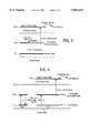
- FIG. 1schematically illustrates a generic two-photon photorefractive holographic recording arrangement according to established principles, including a pump beam, a reference beam, an object beam, and a photorefractive holographic recording medium.
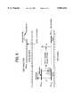
- FIG. 2is a general energy level diagram schematically illustrating a charge transfer process for a photorefractive holographic recording medium in accordance with the present invention including a single-species rare earth dopant suitable for two-photon photorefractive recording.
- FIG. 3is a general energy level diagram schematically illustrating another charge transfer process for a photorefractive holographic recording medium in accordance with the present invention including a single-species rare earth dopant.
- FIG. 4is a general energy level diagram schematically illustrating a two-photon charge transfer process for a photorefractive holographic recording medium in accordance with the present invention including two species of rare earth dopants.
- FIG. 5is a general energy level diagram schematically illustrating another two-photon charge transfer process for a photorefractive holographic recording medium in accordance with the present invention including two species of rare earth dopants.
- FIG. 6is a general energy level diagram schematically illustrating yet another two-photon charge transfer process for a photorefractive holographic recording medium in accordance with the present invention including two species of rare earth dopants.
- the present inventionfocuses on the photoionization step in the photorefractive effect and provides new dopant schemes for achieving multiphoton photorefractive recording.
- the new dopant schemesinvolve lanthanide dopant materials.
- host materialsare doped with one or more lanthanide dopant materials (ions) such that multiphoton absorption produces excitation of at least one dopant ion from its ground state to a higher energy level.
- An excitation pathwaycan involve either real or virtual intermediate energy states, or a combination of the two. Two distinctly different types of multiphoton excitation, termed here as direct and indirect, are possible.
- direct multiphoton excitationan ion of interest is promoted to the higher energy configuration by direct absorption of two or more photons.
- direct two-photon absorption via a real metastable intermediate statea process which may also be referred to as resonant two-step absorption.
- indirect multiphoton excitationinvolves, during at least one step in the process, the promotion of one species of ion (termed an activator) to a higher energy configuration by energy transfer from a neighboring ion of a different species (termed a sensitizer). Therefore, indirect multiphoton excitation involves doping with at least two species of photoactive ions to provide a means for energy transfer. Additional steps in the excitation of the activator (i.e., quantum mechanical energy transitions) can arise from photon absorption by the activator.
- a general two-photon recording arrangementutilizes a recording material or medium 11 and a pump beam 12 of wavelength ⁇ 1 .
- Wavelengths ⁇ 1 and ⁇ 2are preferably provided by relatively low intensity laser beams, formed by focused continuous wave (CW) lasers.
- a low intensity beamis here exemplified as a beam having an intensity less than about 10 7 W/cm 2 .
- a photorefractive holographic recording materialincludes a host material including one or more dopants.
- a host materialincluding one or more dopants.
- the holographic recording materialcontain both filled and empty traps. Maximum dynamic recording is achieved when the relative concentrations of filled and empty traps are about equal.
- Dopant ions in the materialshould exist in more than one valence state in order to provide both filled and empty traps. In a crystalline host material, associated ground states of the dopant ions should lie within the band gap of the host material.
- the relative concentrations of the valence statesmay be controlled during or after fabrication of the recording material, by controlling oxidizing or reducing properties of atmosphere surrounding the material during growth or during post-growth treatment while the material is at an elevated temperature, for example greater than about five-hundred degrees centigrade (500° C.).
- the filled traps in a multiphoton photorefractive holographic recording materialshould possess at least one metastable intermediate energy level having a relatively long excited-state lifetime, preferably between about 10 -6 to 10 -2 seconds.
- the present inventionis directed to the use of lanthanide materials as dopant materials for a multiphoton photorefractive holographic recording material. Ions of the lanthanides have relatively long excited state lifetimes and can satisfy both of the above-discussed criteria. Specific schemes for their implementation in multiphoton photorefractive holographic recording material in accordance with the present invention, as well as aspects related to the choice of a host material are discussed in detail hereinbelow.
- two-photon recordingdoes not necessarily imply two-wavelength recording. Rather, "two-photon” simply refers to the fact that absorption of two individual photons (one for reaching an intermediate state, and another to achieve photoionization from the intermediate state) is involved in the creation of a free charge carrier. Therefore, pump beam 12 and object and reference beams 16 and 18 may contain many discrete wavelengths or a continuum of wavelengths.
- rare earth ions in solidsare known for certain unique spectral properties, perhaps foremost being the extreme sharpness of several absorption and emission lines.
- Lanthanide rare earth ions, when incorporated into solid materials,are most often found to have valence states between +2 and +4 with an electronic configuration given by 4f n 5s 2 5p 6 (the number of f-shell electrons, n, depends on the atomic number of the ion and its valence state). Almost all of the sharp absorption and emission lines are due to transitions within the manifold of the 4f electrons.
- the 4f electronsare not the outermost ones and are shielded from the surroundings by two other electronic shells, the 5s and 5p, which have larger radial extensions. Therefore, the 4f states are only weakly perturbed by the host material, which accounts for the sharp character of the lines. However, the perturbation by the host material is often sufficient to mix states of different parity into the 4f states, thereby allowing 4f ⁇ 4f electric dipole transitions that are otherwise forbidden by the parity selection rule. This interpretation explains the relatively low oscillator strengths as well as the very long lifetimes of the 4f ⁇ 4f transitions. It is also important to note that a few 4f ⁇ 4f magnetic dipole transitions exist and are not forbidden by the parity selection rule. These transitions are much weaker than allowed electric dipole transitions, but they can have oscillator strengths comparable to, if not much larger, than many of the observed "forbidden" electric dipole transitions.
- the next excited-state electronic configuration of the lanthanidesis 4f n-1 5s 2 5p 6 5d.
- the 4f n ⁇ 4f n-1 5d electric dipole transitionsare not forbidden by the parity selection rule and can therefore lead to strong optical absorption.
- the 4f ⁇ 5d transitionstypically lie in the ultraviolet.
- Some rare earth elementssuch as Eu, Sm, and Yb can also exist in a divalent state, in which case the 4f ⁇ 5d transitions lie in the visible and mask the weaker 4f ⁇ 4f transitions.
- the 5d statesstrongly couple to the host material and can therefore participate in a charge transfer process.
- a key aspect of a multiphoton photorefractive holographic recording medium in accordance with the present inventionis that rare earth dopants incorporated in a host material provide a means whereby an electron of the dopant material (ion) may be promoted from a 4f ground state into an upper excited 5d state via a long-lived intermediate 4f state.
- This aspectis illustrated in equation form as:
- the rare earth doping concentration required to observe a photorefractive effect in a photorefractive holographic recording material in accordance with the present inventioncan be expected to lie approximately in a concentration range from about 0.01 to 3.0 mole %, depending on which host material, dopant, and charge transfer (transition) scheme is selected.
- dopant concentrations toward the larger end of this concentration rangecan be used, and, in fact, may be required to offset weak absorption.
- the degree to which the dopant concentration can be increaseddepends on how the dopant is incorporated into the host and what effect doping has on the optical quality of the material.
- charge transfer schemes for a photorefractive holographic recording material doped with a single rare earth species in accordance with the present inventionare described.
- One such schemeprovides an energy level configuration, as shown in FIG. 2, that is particularly amenable to two-photon photorefractive recording.
- the energy levels in FIG. 2are identified by quantum states denoted ⁇ 1>,
- a long-lived intermediate state, or metastable stateis advantageous because the rate at which transitions occur from this state to the second, higher-energy excited state is linearly proportional to the intermediate state lifetime.
- a metastable intermediate stateleads to more efficient two-photon photorefractive recording, with lower optical intensity requirements compared to a short-lived intermediate state.
- FIG. 2specifically illustrates the photoionization process for a rare earth ion acting as a filled electron trap.
- the host material in FIG. 2is assumed to be a ferroelectric crystal.
- ⁇ 2>is populated by illuminating the material with radiation (photons) of wavelength ⁇ 1 which falls within the absorption band of the metastable state.
- the single rare earth species doping approach of FIG. 2therefore centers on direct excitation of the metastable intermediate state through resonant or near-resonant absorption involving a 4f ⁇ 4f transition.
- Photoionizationthen takes place by exciting a 4f ⁇ 5d transition with radiation (photons) of wavelength ⁇ 2 which, through coupling between the 5d state of the rare earth ion and the host crystal, leads to the creation of a free electron in the conduction band.
- An analogous situationexists for the production of a free hole, in which case the rare earth ion has a valence state corresponding to an empty electron trap and a hole is photoionized from the metastable intermediate state. It is pointed out here that only the case of electron photoionization from filled electron traps is illustrated in FIG. 2, and in FIGS. 3, 4, 5, and 6, which illustrate other doping or charge transfer schemes in accordance with the present invention. In all of these schemes, however, hole photoionization may take place from empty electron traps in a similar fashion.
- a metastable intermediate statemay also be populated by exciting a higher-energy intermediate state
- the pumping radiationcan be broadband or can contain multiple wavelengths so that more than one discrete intermediate state or a continuum of intermediate states can be simultaneously excited. Those states lying above
- ⁇ 2>is not restricted to 4f ⁇ 4f transitions and may include 4f ⁇ 5d transitions as long as any photoionization that might also occur be sufficiently small so as not to preclude hologram recording.
- Photorefractive hologram recordingtakes place at wavelength ⁇ 2 during or shortly after illumination with the pumping radiation at wavelength ⁇ 1 (or ⁇ 1 *).
- the object and reference recording pulsescan arrive at the sample simultaneously with the pumping pulse, or they can be delayed with respect to the pumping pulse by a time duration no greater than the lifetime of the metastable intermediate state. This same constraint applies to the erasure radiation, although the erasure radiation need not derive from the same source as the recording radiation.
- Table 1contains a partial list of candidate lanthanide ions any one of which is useful in single-species doping in two-photon photorefractive holographic recording material in accordance with the present invention.
- Table 1The various energy levels in Table 1 are given in conventional Russell-Sanders term notation ( 2S+1 L J ). Listed are the ground state
- msmilliseconds
- FIG. 2The case of resonant or near-resonant excitation of the metastable intermediate state (FIG. 2) occurs when
- ⁇ 2>*
- ⁇ 2> and ⁇ 1 *⁇ 1 .
- wavelengths listed in Table 2are wavelengths which would be required for pump beam 12 of FIG. 1 and are primarily visible wavelengths.
- Wavelengths for object beam 16lie in a range from about 400 to 1500 nm a range. These wavelengths may readily be determined from sample materials, for example, by means of two-photon spectroscopy using a monochromator in conjunction with a high-intensity light source such as an arc lamp for each of two tuneable sources.
- charge transfer schemes for a photorefractive holographic recording material doped with two different rare earth species in accordance with the present inventionare described. These schemes may be referred to as dual-species doping schemes. In these schemes, energy contained in the excited state of one type of dopant ion (the sensitizer) is transferred to a second type of dopant ion (the activator, assumed to be a rare earth ion) in order to facilitate charge transfer. So, for example, absorption of a photon by the sensitizer and transfer of this energy to the activator can be considered to constitute the first step of a two-photon photoionization process.
- This dual-species doping techniqueis most useful when the intermediate excited state of the second type of ion is more efficiently populated by energy transfer than by direct absorption of a photon.
- preferred combinations of lanthanide dopant materialsare Pr/Sm, Pr/Eu, Eu/Tb, and Yb/Pr.
- multiphoton photorefractive recordingcan be made to occur in a dual-species doped material, even though the requisite
- a transition schemeis presented wherein energy is transferred from the excited state of Ion A (the sensitizer) to Ion B (the activator), placing Ion B in a metastable intermediate state. If the transitions
- the temperature of the host materialmust be sufficient to provide the necessary reservoir of phonons throughout the material.
- Ion Bonce Ion B reaches the intermediate state
- the 2 F 5/2 excited state in Yb 3+can transfer energy to the 1 G 4 level of Pr 3+ , thereby populating this intermediate level and allowing for further excitation into the 5d levels of Pr 3+ .
- excitation of the activatorcan take place with a photon of wavelength ⁇ 1 * which has a higher energy than the transition associated with the energy transfer step.
- excitation of Ion Amay occur to any of a plurality of levels above the intermediate state
- ⁇ 2> Athen occurs, followed by energy transfer to Ion B (producing state
- FIG. 6Yet another energy transfer scheme is depicted in FIG. 6.
- the excited state of Ion Adoes not transfer its energy to a real intermediate state of Ion B. Instead, Ion A gives up its energy in such a way that when combined with the simultaneous absorption of a photon having the proper energy, the net energy is sufficient to excite Ion B directly into the upper state, leading to charge transfer.
- This cooperative transfer phenomenonis referred to as photon-assisted energy transfer. It is utilized when an ion with the desired photorefractive properties is identified, e.g., an ion which may readily exhibit two valence states, thereby allowing for the proper combination of filled and empty traps, but for which no suitable intermediate excited states exist to provide for direct multiphoton absorption.
- the crystal lattice of the hostshould be able to accommodate the dopant or dopants of interest, either by substitution for lattice ions or in interstitial locations.
- the host materialshould be an electro-optic material which provides a large polarization-optic coefficient f eff given by
- r effis the effective linear electro-optic coefficient
- ⁇is the relative static dielectric constant
- ⁇ 0is the free-space permittivity.
- f effshould be no smaller than about 0.02 square meters per coulomb (m 2 /C).
- the doped host materialshould also provide a high photorefractive sensitivity (defined as the refractive index change per absorbed unit energy) and large dynamic range (maximum photorefractive index change) when used in real-time applications such as read/write data storage; although for other applications such as holographic spectral filtering, the photorefractive sensitivity is not as critical.
- Material physics that determine the sensitivity and dynamic rangeare thoroughly documented in scientific literature, for example in Photorefractive Materials and Their Applications I, Springer-Verlag, 1989.
- Ferroelectric oxides materialssatisfy most of the above discussed host requirements.
- Typical ferroelectric materials that are suitable for use in this inventioninclude lithium niobate (LiNbO 3 ), barium titanate (BaTiO 3 ), potassium tantalate niobate (KTN), and materials having a tungsten bronze crystal structure such as strontium barium niobate (SBN), barium strontium potassium sodium niobate (BSKNN).
- Doped single crystals of these ferroelectric oxidesmay be grown by any suitable established method, for example, Czochralski, Bridgman, laser-heated pedestal growth, or top-seeded solution growth.
- the relative ionic radii in ⁇ ngstrom units ( ⁇ .U.) of the dopant ion or ions and the lattice ions that are being displacedshould ideally be similar in value.
- the ionic radii of the rare earth lanthanide ionsare given in Tables 2 and 3. It can be seen that their values are generally in the range from 1.0-1.2 ⁇ .U..
- Table 4lists the ionic radii ( ⁇ .U.) of the various ferroelectric constituent ions.
- ferroelectricscomprising Sr 2+ and/or Ba 2+ (such as SBN or BSKNN) are particularly well-suited for rare earth doping.
- SBN or BSKNNferroelectrics comprising Sr 2+ and/or Ba 2+
- other materialssuch as LiNbO 3 can not be adequately doped with one or more of the rare earths to provide a multiphoton photorefractive holographic recording material.
- the host materialneed not be a ferroelectric single crystal. It may also be a polycrystalline, electro-optic, ceramic material such as lead lanthanum zirconate titanate ((Pb 1-x , La x )(Zr y ,Ti z )O 3 or PLZT), or an amorphous material such as an electro-optic photorefractive polymer.
- a polycrystalline, electro-optic, ceramic materialsuch as lead lanthanum zirconate titanate ((Pb 1-x , La x )(Zr y ,Ti z )O 3 or PLZT), or an amorphous material such as an electro-optic photorefractive polymer.
- one family of such polymersis based on poly-(N-vinylcarbazole) (PVK) light sensitized by addition of 2,4,7,-trinitro-9-fluorenone (TNF), and provided with electro-optic properties by addition of an azo dye 2,5-dimethyl-4-(p-nitrophenylazo)anisole (DMNPAA).
- PVKpoly-(N-vinylcarbazole)
- TNF2,4,7,-trinitro-9-fluorenone
- DMNPAA2,5-dimethyl-4-(p-nitrophenylazo)anisole
- the host materialmay be any material which can be doped with one or more lanthanide materials and which exhibits an electro-optic effect.
- the host materialmay be any material which can be doped with one or more lanthanide materials and which exhibits an electro-optic effect.
- a single-species or dual-species doping schemecan be employed in a wide variety of host materials.
- Some materialsof course will prove more advantageous than others depending on criteria such as ease and cost of material fabrication, electro-optic properties, the manner in which the dopant enters the host material, and the desired optical quality of the recording material.
- two different ferroelectric crystal materials, LiNbO 3 , and SBNare preferred as host materials for multiphoton photorefractive holographic recording medium in accordance with the present invention.
- SBNis better suited than LiNbO 3 for incorporation of the lanthanides.
- SBNhas larger electro-optic coefficients than LiNbO 3 .
- SBNis much more difficult and costly to grow with high optical quality compared to LiNbO 3 , primarily due its very high melting temperature (about 1500° C.), highly anisotropic growth kinetics, and strong tendency to striation formation.
- LiNbO 3is a commonly available electro-optic crystal that can be readily grown with a very high optical quality.
Landscapes
- Engineering & Computer Science (AREA)
- Physics & Mathematics (AREA)
- Chemical & Material Sciences (AREA)
- Nanotechnology (AREA)
- Mathematical Physics (AREA)
- Theoretical Computer Science (AREA)
- Crystallography & Structural Chemistry (AREA)
- General Physics & Mathematics (AREA)
- Holo Graphy (AREA)
Abstract
Description
|4f.sup.n >→|4f.sup.n >*→|4f.sup.n-1 5d>*→CT (1)
TABLE 1______________________________________Ion |Ψ1> |Ψ2>* λ.sub.1 * (nm) |Ψ2> τ (ms)______________________________________Pr.sup.3+ .sup.3 H.sub.4 .sup.1 I.sub.6 470 .sup.3 P.sub.0 0.01 .sup.3 P.sub.1 475 .sup.3 P.sub.0 490 .sup.1 D.sub.2 600 .sup.1 D.sub.2 0.2 .sup.3 P.sub.0 475Sm.sup.3+ .sup.6 H.sub.5/2 .sup.4 G.sub.5/2 560 .sup.4 G.sub.5/2 1.0 .sup.4 F.sub.3/2 530 .sup.4 G.sub.7/2 500Sm.sup.2+ .sup.7 F.sub.0 .sup.5 D.sub.2 575 .sup.5 D.sub.0 1.0 .sup.5 D.sub.1 630 .sup.5 D.sub.0 690Eu.sup.3+ .sup.7 F.sub.0 .sup.5 D.sub.2 465 .sup.5 D.sub.0 1.0 .sup.5 D.sub.1 526 .sup.5 D.sub.0 579Tb.sup.3+ .sup.7 F.sub.6 .sup.5 D.sub.4 488 .sup.5 D.sub.4 1.3 .sup.5 D.sub.3 381______________________________________
f.sub.eff =r.sub.eff /εε.sub.0 (2)
TABLE 2______________________________________Valence Ce Pr Nd Pm Sm Eu Gd______________________________________2+ 1.24 1.23 1.21 1.20 1.18 1.17 1.163+ 1.02 1.00 0.99 0.98 0.97 0.97 0.97______________________________________
TABLE 3______________________________________Valence Tb Dy Ho Er Tm Yb______________________________________2+ 1.14 1.13 1.11 1.10 1.08 1.073+ 1.00 0.99 0.97 0.96 0.95 0.94______________________________________
TABLE 4______________________________________Ion Radius (Å.U.)______________________________________Li.sup.+ 0.60Nb.sup.5+ 0.70Sr.sup.5+ 1.13Ba.sup.2+ 1.35Ti.sup.4+ 0.68Na.sup.+ 0.95K.sup.+ 1.33______________________________________
Claims (20)
Priority Applications (1)
| Application Number | Priority Date | Filing Date | Title |
|---|---|---|---|
| US08/847,727US5864412A (en) | 1995-09-08 | 1997-04-28 | Multiphoton photorefractive holographic recording media |
Applications Claiming Priority (2)
| Application Number | Priority Date | Filing Date | Title |
|---|---|---|---|
| US08/525,823US5699175A (en) | 1995-09-08 | 1995-09-08 | Multiphoton photorefractive holographic recording media |
| US08/847,727US5864412A (en) | 1995-09-08 | 1997-04-28 | Multiphoton photorefractive holographic recording media |
Related Parent Applications (1)
| Application Number | Title | Priority Date | Filing Date |
|---|---|---|---|
| US08/525,823ContinuationUS5699175A (en) | 1995-09-08 | 1995-09-08 | Multiphoton photorefractive holographic recording media |
Publications (1)
| Publication Number | Publication Date |
|---|---|
| US5864412Atrue US5864412A (en) | 1999-01-26 |
Family
ID=24094748
Family Applications (2)
| Application Number | Title | Priority Date | Filing Date |
|---|---|---|---|
| US08/525,823Expired - Fee RelatedUS5699175A (en) | 1995-09-08 | 1995-09-08 | Multiphoton photorefractive holographic recording media |
| US08/847,727Expired - LifetimeUS5864412A (en) | 1995-09-08 | 1997-04-28 | Multiphoton photorefractive holographic recording media |
Family Applications Before (1)
| Application Number | Title | Priority Date | Filing Date |
|---|---|---|---|
| US08/525,823Expired - Fee RelatedUS5699175A (en) | 1995-09-08 | 1995-09-08 | Multiphoton photorefractive holographic recording media |
Country Status (1)
| Country | Link |
|---|---|
| US (2) | US5699175A (en) |
Cited By (40)
| Publication number | Priority date | Publication date | Assignee | Title |
|---|---|---|---|---|
| US5978108A (en)* | 1997-03-12 | 1999-11-02 | Stanford Research Institute | Two-step gated holographic recording in photorefractive materials using cw lasers |
| US6157470A (en)* | 1998-02-26 | 2000-12-05 | California Institute Of Technology | Non-volatile holographic storage in doubly-doped photorefractive material |
| WO2001057571A1 (en)* | 2000-02-03 | 2001-08-09 | The University Of Sydney | Inducing change of refractive index by differing radiations |
| US20030194651A1 (en)* | 2000-06-15 | 2003-10-16 | De Voe Robert J. | Multicolor imaging using multiphoton photochemical processes |
| US20040012872A1 (en)* | 2001-06-14 | 2004-01-22 | Fleming Patrick R | Multiphoton absorption method using patterned light |
| US20040028101A1 (en)* | 2002-08-06 | 2004-02-12 | Byren Robert W. | Solid-state devices with radial dopant valence profile |
| US20040042937A1 (en)* | 2000-06-15 | 2004-03-04 | Bentsen James G | Process for producing microfluidic articles |
| US20040126694A1 (en)* | 2000-06-15 | 2004-07-01 | Devoe Robert J. | Microfabrication of organic optical elements |
| US20040124563A1 (en)* | 2000-06-15 | 2004-07-01 | Fleming Patrick R. | Multipass multiphoton absorption method and apparatus |
| US20040223385A1 (en)* | 2000-06-15 | 2004-11-11 | Fleming Patrick R. | Multidirectional photoreactive absorption method |
| US6852766B1 (en) | 2000-06-15 | 2005-02-08 | 3M Innovative Properties Company | Multiphoton photosensitization system |
| US6867408B1 (en)* | 1999-02-17 | 2005-03-15 | Victoria University Of Technology | Erasable/rewritable optical data storage with photorefractive polymers |
| US20050208431A1 (en)* | 2000-06-15 | 2005-09-22 | Devoe Robert J | Multiphoton curing to provide encapsulated optical elements |
| US20050243592A1 (en)* | 2004-04-16 | 2005-11-03 | Rust Thomas F | High density data storage device having eraseable bit cells |
| US20060291271A1 (en)* | 2005-06-24 | 2006-12-28 | Nanochip, Inc. | High density data storage devices having servo indicia formed in a patterned media |
| US20070008867A1 (en)* | 2005-07-08 | 2007-01-11 | Nanochip, Inc. | High density data storage devices with a lubricant layer comprised of a field of polymer chains |
| US20070008865A1 (en)* | 2005-07-08 | 2007-01-11 | Nanochip, Inc. | High density data storage devices with polarity-dependent memory switching media |
| US20070121477A1 (en)* | 2006-06-15 | 2007-05-31 | Nanochip, Inc. | Cantilever with control of vertical and lateral position of contact probe tip |
| US20070285763A1 (en)* | 2006-06-09 | 2007-12-13 | Kewen Kevin Li | Electro-optic gain ceramic and lossless devices |
| US20070291623A1 (en)* | 2006-06-15 | 2007-12-20 | Nanochip, Inc. | Cantilever with control of vertical and lateral position of contact probe tip |
| US20070290282A1 (en)* | 2006-06-15 | 2007-12-20 | Nanochip, Inc. | Bonded chip assembly with a micro-mover for microelectromechanical systems |
| US20080001075A1 (en)* | 2006-06-15 | 2008-01-03 | Nanochip, Inc. | Memory stage for a probe storage device |
| US20080074792A1 (en)* | 2006-09-21 | 2008-03-27 | Nanochip, Inc. | Control scheme for a memory device |
| US20080074984A1 (en)* | 2006-09-21 | 2008-03-27 | Nanochip, Inc. | Architecture for a Memory Device |
| US20080151358A1 (en)* | 2006-06-09 | 2008-06-26 | Hua Jiang | Transparent electro-optic gain ceramics and devices |
| US20080165568A1 (en)* | 2002-10-15 | 2008-07-10 | Nanochip, Inc. | Probes and Media for High Density Data Storage |
| US20080175033A1 (en)* | 2007-01-19 | 2008-07-24 | Nanochip, Inc. | Method and system for improving domain stability in a ferroelectric media |
| US20080174918A1 (en)* | 2007-01-19 | 2008-07-24 | Nanochip, Inc. | Method and system for writing and reading a charge-trap media with a probe tip |
| US20080232228A1 (en)* | 2007-03-20 | 2008-09-25 | Nanochip, Inc. | Systems and methods of writing and reading a ferro-electric media with a probe tip |
| US20080233672A1 (en)* | 2007-03-20 | 2008-09-25 | Nanochip, Inc. | Method of integrating mems structures and cmos structures using oxide fusion bonding |
| US20080318086A1 (en)* | 2007-06-19 | 2008-12-25 | Nanochip, Inc. | Surface-treated ferroelectric media for use in systems for storing information |
| US20080316897A1 (en)* | 2007-06-19 | 2008-12-25 | Nanochip, Inc. | Methods of treating a surface of a ferroelectric media |
| US20090021975A1 (en)* | 2007-07-16 | 2009-01-22 | Valluri Ramana Rao | Method and media for improving ferroelectric domain stability in an information storage device |
| US20090201015A1 (en)* | 2008-02-12 | 2009-08-13 | Nanochip, Inc. | Method and device for detecting ferroelectric polarization |
| US20090213492A1 (en)* | 2008-02-22 | 2009-08-27 | Nanochip, Inc. | Method of improving stability of domain polarization in ferroelectric thin films |
| US20090294028A1 (en)* | 2008-06-03 | 2009-12-03 | Nanochip, Inc. | Process for fabricating high density storage device with high-temperature media |
| US20100002563A1 (en)* | 2008-07-01 | 2010-01-07 | Nanochip, Inc. | Media with tetragonally-strained recording layer having improved surface roughness |
| US20100039919A1 (en)* | 2008-08-15 | 2010-02-18 | Nanochip, Inc. | Cantilever Structure for Use in Seek-and-Scan Probe Storage |
| US20100068509A1 (en)* | 2008-09-17 | 2010-03-18 | Nanochip, Inc. | Media having improved surface smoothness and methods for making the same |
| US20100085863A1 (en)* | 2008-10-07 | 2010-04-08 | Nanochip, Inc. | Retuning of ferroelectric media built-in-bias |
Families Citing this family (8)
| Publication number | Priority date | Publication date | Assignee | Title |
|---|---|---|---|---|
| US5699175A (en)* | 1995-09-08 | 1997-12-16 | Quinta Corporation | Multiphoton photorefractive holographic recording media |
| US5847851A (en)* | 1997-03-06 | 1998-12-08 | Hughes Electronics Corporation | Double-doped BaTiO3 crystal for holographic storage |
| US6028835A (en)* | 1998-11-03 | 2000-02-22 | Thomas; Michael E. | Integrated read/write head for ferroelectric optical storage |
| US6046973A (en)* | 1999-01-07 | 2000-04-04 | Thomas; Michael E. | Integrated read/write head for ferroelectric optical media |
| JP4139881B2 (en)* | 1999-06-24 | 2008-08-27 | 独立行政法人物質・材料研究機構 | Photorefractive material |
| US6624915B1 (en)* | 2000-03-16 | 2003-09-23 | Science Applications International Corporation | Holographic recording and micro/nanofabrication via ultrafast holographic two-photon induced photopolymerization (H-TPIP) |
| JP3728410B2 (en)* | 2001-09-07 | 2005-12-21 | 独立行政法人物質・材料研究機構 | Hologram recording medium pretreatment method |
| US20040259030A1 (en)* | 2003-06-23 | 2004-12-23 | Hayden Joseph S. | Resonantly enhanced photosensitivity |
Citations (6)
| Publication number | Priority date | Publication date | Assignee | Title |
|---|---|---|---|---|
| US4953924A (en)* | 1987-12-30 | 1990-09-04 | Microelectronics And Computer Technology Corporation | Enhanced nondestructive holographic reconstruction |
| US5440669A (en)* | 1991-07-26 | 1995-08-08 | Accuwave Corporation | Photorefractive systems and methods |
| US5665493A (en)* | 1995-10-03 | 1997-09-09 | Sri International | Gated recording of holograms using rare-earth doped ferroelectric materials |
| US5684612A (en)* | 1993-06-11 | 1997-11-04 | Board Of Trustees Of The Leland Stanford Junior University | Method and system for maintaining and controlling the signal-to-noise ratio of hologams recorded in ferroelectric photorefractive materials |
| US5699175A (en)* | 1995-09-08 | 1997-12-16 | Quinta Corporation | Multiphoton photorefractive holographic recording media |
| US5698344A (en)* | 1995-11-28 | 1997-12-16 | Sri International | Two-step gated holographic recording in photorefractive materials using cw lasers |
Family Cites Families (5)
| Publication number | Priority date | Publication date | Assignee | Title |
|---|---|---|---|---|
| US3544189A (en)* | 1968-06-12 | 1970-12-01 | Bell Telephone Labor Inc | Holography using a poled ferroelectric recording material |
| US3915549A (en)* | 1971-11-08 | 1975-10-28 | Rca Corp | Crystals for recording phase holograms |
| US3997350A (en)* | 1973-03-27 | 1976-12-14 | Mitsubishi Denki Kabushiki Kaisha | Holographic storage material |
| US3922061A (en)* | 1974-06-10 | 1975-11-25 | Bell Telephone Labor Inc | Optical storage apparatus and process |
| US4052119A (en)* | 1976-03-29 | 1977-10-04 | Rca Corporation | Crystals for recording phase holograms |
- 1995
- 1995-09-08USUS08/525,823patent/US5699175A/ennot_activeExpired - Fee Related
- 1997
- 1997-04-28USUS08/847,727patent/US5864412A/ennot_activeExpired - Lifetime
Patent Citations (6)
| Publication number | Priority date | Publication date | Assignee | Title |
|---|---|---|---|---|
| US4953924A (en)* | 1987-12-30 | 1990-09-04 | Microelectronics And Computer Technology Corporation | Enhanced nondestructive holographic reconstruction |
| US5440669A (en)* | 1991-07-26 | 1995-08-08 | Accuwave Corporation | Photorefractive systems and methods |
| US5684612A (en)* | 1993-06-11 | 1997-11-04 | Board Of Trustees Of The Leland Stanford Junior University | Method and system for maintaining and controlling the signal-to-noise ratio of hologams recorded in ferroelectric photorefractive materials |
| US5699175A (en)* | 1995-09-08 | 1997-12-16 | Quinta Corporation | Multiphoton photorefractive holographic recording media |
| US5665493A (en)* | 1995-10-03 | 1997-09-09 | Sri International | Gated recording of holograms using rare-earth doped ferroelectric materials |
| US5698344A (en)* | 1995-11-28 | 1997-12-16 | Sri International | Two-step gated holographic recording in photorefractive materials using cw lasers |
Cited By (57)
| Publication number | Priority date | Publication date | Assignee | Title |
|---|---|---|---|---|
| US5978108A (en)* | 1997-03-12 | 1999-11-02 | Stanford Research Institute | Two-step gated holographic recording in photorefractive materials using cw lasers |
| US6157470A (en)* | 1998-02-26 | 2000-12-05 | California Institute Of Technology | Non-volatile holographic storage in doubly-doped photorefractive material |
| US6867408B1 (en)* | 1999-02-17 | 2005-03-15 | Victoria University Of Technology | Erasable/rewritable optical data storage with photorefractive polymers |
| WO2001057571A1 (en)* | 2000-02-03 | 2001-08-09 | The University Of Sydney | Inducing change of refractive index by differing radiations |
| US20030113064A1 (en)* | 2000-02-03 | 2003-06-19 | Leon Poladian | Inducing change of refractive index by differing radiations |
| US20040124563A1 (en)* | 2000-06-15 | 2004-07-01 | Fleming Patrick R. | Multipass multiphoton absorption method and apparatus |
| US20060078831A1 (en)* | 2000-06-15 | 2006-04-13 | 3M Innovative Properties Company | Multiphoton curing to provide encapsulated optical elements |
| US20040042937A1 (en)* | 2000-06-15 | 2004-03-04 | Bentsen James G | Process for producing microfluidic articles |
| US20040126694A1 (en)* | 2000-06-15 | 2004-07-01 | Devoe Robert J. | Microfabrication of organic optical elements |
| US7601484B2 (en) | 2000-06-15 | 2009-10-13 | 3M Innovative Properties Company | Multiphoton curing to provide encapsulated optical elements |
| US20040223385A1 (en)* | 2000-06-15 | 2004-11-11 | Fleming Patrick R. | Multidirectional photoreactive absorption method |
| US6852766B1 (en) | 2000-06-15 | 2005-02-08 | 3M Innovative Properties Company | Multiphoton photosensitization system |
| US6855478B2 (en) | 2000-06-15 | 2005-02-15 | 3M Innovative Properties Company | Microfabrication of organic optical elements |
| US20050054744A1 (en)* | 2000-06-15 | 2005-03-10 | 3M Innovative Properties Company | Multiphoton photosensitization system |
| US20100027956A1 (en)* | 2000-06-15 | 2010-02-04 | 3M Innovative Properties Company | Multiphoton curing to provide encapsulated optical elements |
| US20050208431A1 (en)* | 2000-06-15 | 2005-09-22 | Devoe Robert J | Multiphoton curing to provide encapsulated optical elements |
| US7790353B2 (en) | 2000-06-15 | 2010-09-07 | 3M Innovative Properties Company | Multidirectional photoreactive absorption method |
| US8530118B2 (en) | 2000-06-15 | 2013-09-10 | 3M Innovative Properties Company | Multiphoton curing to provide encapsulated optical elements |
| US7014988B2 (en) | 2000-06-15 | 2006-03-21 | 3M Innovative Properties Company | Multiphoton curing to provide encapsulated optical elements |
| US7026103B2 (en) | 2000-06-15 | 2006-04-11 | 3M Innovative Properties Company | Multicolor imaging using multiphoton photochemical processes |
| US20030194651A1 (en)* | 2000-06-15 | 2003-10-16 | De Voe Robert J. | Multicolor imaging using multiphoton photochemical processes |
| US7060419B2 (en) | 2000-06-15 | 2006-06-13 | 3M Innovative Properties Company | Process for producing microfluidic articles |
| US7091255B2 (en) | 2000-06-15 | 2006-08-15 | 3M Innovative Properties Company | Multiphoton photosensitization system |
| US7166409B2 (en) | 2000-06-15 | 2007-01-23 | 3M Innovative Properties Company | Multipass multiphoton absorption method and apparatus |
| US20040012872A1 (en)* | 2001-06-14 | 2004-01-22 | Fleming Patrick R | Multiphoton absorption method using patterned light |
| US20040028101A1 (en)* | 2002-08-06 | 2004-02-12 | Byren Robert W. | Solid-state devices with radial dopant valence profile |
| US6996137B2 (en)* | 2002-08-06 | 2006-02-07 | Raytheon Company | Solid-state devices with radial dopant valence profile |
| US20080165568A1 (en)* | 2002-10-15 | 2008-07-10 | Nanochip, Inc. | Probes and Media for High Density Data Storage |
| US20050243592A1 (en)* | 2004-04-16 | 2005-11-03 | Rust Thomas F | High density data storage device having eraseable bit cells |
| US20060291271A1 (en)* | 2005-06-24 | 2006-12-28 | Nanochip, Inc. | High density data storage devices having servo indicia formed in a patterned media |
| US20070008867A1 (en)* | 2005-07-08 | 2007-01-11 | Nanochip, Inc. | High density data storage devices with a lubricant layer comprised of a field of polymer chains |
| US20070008865A1 (en)* | 2005-07-08 | 2007-01-11 | Nanochip, Inc. | High density data storage devices with polarity-dependent memory switching media |
| US20070285763A1 (en)* | 2006-06-09 | 2007-12-13 | Kewen Kevin Li | Electro-optic gain ceramic and lossless devices |
| US7791791B2 (en) | 2006-06-09 | 2010-09-07 | Boston Applied Technologies, Incorporated | Transparent electro-optic gain ceramics and devices |
| US20090168150A1 (en)* | 2006-06-09 | 2009-07-02 | Kewen Kevin Li | Electro-optic gain ceramic and lossless devices |
| US20080151358A1 (en)* | 2006-06-09 | 2008-06-26 | Hua Jiang | Transparent electro-optic gain ceramics and devices |
| US20070121477A1 (en)* | 2006-06-15 | 2007-05-31 | Nanochip, Inc. | Cantilever with control of vertical and lateral position of contact probe tip |
| US20070291623A1 (en)* | 2006-06-15 | 2007-12-20 | Nanochip, Inc. | Cantilever with control of vertical and lateral position of contact probe tip |
| US20070290282A1 (en)* | 2006-06-15 | 2007-12-20 | Nanochip, Inc. | Bonded chip assembly with a micro-mover for microelectromechanical systems |
| US20080001075A1 (en)* | 2006-06-15 | 2008-01-03 | Nanochip, Inc. | Memory stage for a probe storage device |
| US20080074792A1 (en)* | 2006-09-21 | 2008-03-27 | Nanochip, Inc. | Control scheme for a memory device |
| US20080074984A1 (en)* | 2006-09-21 | 2008-03-27 | Nanochip, Inc. | Architecture for a Memory Device |
| US20080175033A1 (en)* | 2007-01-19 | 2008-07-24 | Nanochip, Inc. | Method and system for improving domain stability in a ferroelectric media |
| US20080174918A1 (en)* | 2007-01-19 | 2008-07-24 | Nanochip, Inc. | Method and system for writing and reading a charge-trap media with a probe tip |
| US20080232228A1 (en)* | 2007-03-20 | 2008-09-25 | Nanochip, Inc. | Systems and methods of writing and reading a ferro-electric media with a probe tip |
| US20080233672A1 (en)* | 2007-03-20 | 2008-09-25 | Nanochip, Inc. | Method of integrating mems structures and cmos structures using oxide fusion bonding |
| US20080318086A1 (en)* | 2007-06-19 | 2008-12-25 | Nanochip, Inc. | Surface-treated ferroelectric media for use in systems for storing information |
| US20080316897A1 (en)* | 2007-06-19 | 2008-12-25 | Nanochip, Inc. | Methods of treating a surface of a ferroelectric media |
| US7626846B2 (en) | 2007-07-16 | 2009-12-01 | Nanochip, Inc. | Method and media for improving ferroelectric domain stability in an information storage device |
| US20090021975A1 (en)* | 2007-07-16 | 2009-01-22 | Valluri Ramana Rao | Method and media for improving ferroelectric domain stability in an information storage device |
| US20090201015A1 (en)* | 2008-02-12 | 2009-08-13 | Nanochip, Inc. | Method and device for detecting ferroelectric polarization |
| US20090213492A1 (en)* | 2008-02-22 | 2009-08-27 | Nanochip, Inc. | Method of improving stability of domain polarization in ferroelectric thin films |
| US20090294028A1 (en)* | 2008-06-03 | 2009-12-03 | Nanochip, Inc. | Process for fabricating high density storage device with high-temperature media |
| US20100002563A1 (en)* | 2008-07-01 | 2010-01-07 | Nanochip, Inc. | Media with tetragonally-strained recording layer having improved surface roughness |
| US20100039919A1 (en)* | 2008-08-15 | 2010-02-18 | Nanochip, Inc. | Cantilever Structure for Use in Seek-and-Scan Probe Storage |
| US20100068509A1 (en)* | 2008-09-17 | 2010-03-18 | Nanochip, Inc. | Media having improved surface smoothness and methods for making the same |
| US20100085863A1 (en)* | 2008-10-07 | 2010-04-08 | Nanochip, Inc. | Retuning of ferroelectric media built-in-bias |
Also Published As
| Publication number | Publication date |
|---|---|
| US5699175A (en) | 1997-12-16 |
Similar Documents
| Publication | Publication Date | Title |
|---|---|---|
| US5864412A (en) | Multiphoton photorefractive holographic recording media | |
| Bai et al. | Nonvolatile holographic storage with two-step recording in lithium niobate using cw lasers | |
| US5665493A (en) | Gated recording of holograms using rare-earth doped ferroelectric materials | |
| AU711765B2 (en) | Two-step gated holographic recording in photorefractive materials using CW lasers | |
| US5978108A (en) | Two-step gated holographic recording in photorefractive materials using cw lasers | |
| US3932299A (en) | Method for the reduction of iron in iron-doped lithium niobate crystals | |
| EP1565969A2 (en) | Passive q-switch laser | |
| Kiss | Photochromics | |
| JP3963333B2 (en) | Method and apparatus for holographic storage | |
| Basiev et al. | Colour centre lasers | |
| Arizmendi et al. | LiNbO3: A paradigm for photorefractive materials | |
| Lee et al. | Photochromic effect in near-stoichiometric LiNbO 3 and two-color holographic recording | |
| US5847851A (en) | Double-doped BaTiO3 crystal for holographic storage | |
| Duncan et al. | Inorganic photochromic materials | |
| Kim et al. | Volume holographic storage in near-stoichiometric LiNbO3: Ce, Mn | |
| Foldvari et al. | Characteristics of the photorefractive effect in Bi2TeO5 | |
| Staebler | Oxide optical memories: Photochromism and index change | |
| Krätzig et al. | Two-Step processes and IR recording in photorefractive crystals | |
| Schwartz et al. | Spectroscopic properties of photorefractive BaTiO 3 double doped with cerium and rhodium | |
| Sugiyama et al. | Holographic recording in cerium doped strontium barium niobate a-axis single crystal fibers | |
| CA2237182A1 (en) | Two-step gated holographic recording in photorefractive materials using cw lasers | |
| Hasan et al. | Photon-gated holeburning materials: directions in high density memory storage | |
| WO2003087441A1 (en) | Photonic bandgap phosphors and devices | |
| Demirbilek et al. | Investigation of two‐center holographic recording in SBN: Ce: Cr and SBN: Mn: Fe | |
| Bai et al. | Two-step photorefractive effect in rare-earth-doped ferroelectric crystals |
Legal Events
| Date | Code | Title | Description |
|---|---|---|---|
| AS | Assignment | Owner name:SEAGATE TECHNOLOGY, INC., CALIFORNIA Free format text:ASSIGNMENT OF ASSIGNORS INTEREST;ASSIGNOR:QUINTA CORPORATION;REEL/FRAME:009097/0896 Effective date:19980330 | |
| STCF | Information on status: patent grant | Free format text:PATENTED CASE | |
| AS | Assignment | Owner name:SEAGATE TECHNOLOGY LLC, CALIFORNIA Free format text:ASSIGNMENT OF ASSIGNORS INTEREST;ASSIGNOR:SEAGATE TECHNOLOGY, INC.;REEL/FRAME:011077/0319 Effective date:20000728 | |
| AS | Assignment | Owner name:THE CHASE MANHATTAN BANK, AS COLLATERAL AGENT, NEW Free format text:SECURITY AGREEMENT;ASSIGNOR:SEAGATE TECHNOLOGY LLC;REEL/FRAME:011461/0001 Effective date:20001122 | |
| FPAY | Fee payment | Year of fee payment:4 | |
| AS | Assignment | Owner name:JPMORGAN CHASE BANK, AS COLLATERAL AGENT, NEW YORK Free format text:SECURITY AGREEMENT;ASSIGNOR:SEAGATE TECHNOLOGY LLC;REEL/FRAME:013177/0001 Effective date:20020513 Owner name:JPMORGAN CHASE BANK, AS COLLATERAL AGENT,NEW YORK Free format text:SECURITY AGREEMENT;ASSIGNOR:SEAGATE TECHNOLOGY LLC;REEL/FRAME:013177/0001 Effective date:20020513 | |
| AS | Assignment | Owner name:SEAGATE TECHNOLOGY LLC, CALIFORNIA Free format text:RELEASE OF SECURITY INTERESTS IN PATENT RIGHTS;ASSIGNOR:JPMORGAN CHASE BANK, N.A. (FORMERLY KNOWN AS THE CHASE MANHATTAN BANK AND JPMORGAN CHASE BANK), AS ADMINISTRATIVE AGENT;REEL/FRAME:016945/0679 Effective date:20051130 | |
| FPAY | Fee payment | Year of fee payment:8 | |
| AS | Assignment | Owner name:WELLS FARGO BANK, NATIONAL ASSOCIATION, AS COLLATERAL AGENT AND SECOND PRIORITY REPRESENTATIVE, CALIFORNIA Free format text:SECURITY AGREEMENT;ASSIGNORS:MAXTOR CORPORATION;SEAGATE TECHNOLOGY LLC;SEAGATE TECHNOLOGY INTERNATIONAL;REEL/FRAME:022757/0017 Effective date:20090507 Owner name:JPMORGAN CHASE BANK, N.A., AS ADMINISTRATIVE AGENT AND FIRST PRIORITY REPRESENTATIVE, NEW YORK Free format text:SECURITY AGREEMENT;ASSIGNORS:MAXTOR CORPORATION;SEAGATE TECHNOLOGY LLC;SEAGATE TECHNOLOGY INTERNATIONAL;REEL/FRAME:022757/0017 Effective date:20090507 Owner name:JPMORGAN CHASE BANK, N.A., AS ADMINISTRATIVE AGENT Free format text:SECURITY AGREEMENT;ASSIGNORS:MAXTOR CORPORATION;SEAGATE TECHNOLOGY LLC;SEAGATE TECHNOLOGY INTERNATIONAL;REEL/FRAME:022757/0017 Effective date:20090507 Owner name:WELLS FARGO BANK, NATIONAL ASSOCIATION, AS COLLATE Free format text:SECURITY AGREEMENT;ASSIGNORS:MAXTOR CORPORATION;SEAGATE TECHNOLOGY LLC;SEAGATE TECHNOLOGY INTERNATIONAL;REEL/FRAME:022757/0017 Effective date:20090507 | |
| FPAY | Fee payment | Year of fee payment:12 | |
| AS | Assignment | Owner name:MAXTOR CORPORATION, CALIFORNIA Free format text:RELEASE;ASSIGNOR:JPMORGAN CHASE BANK, N.A., AS ADMINISTRATIVE AGENT;REEL/FRAME:025662/0001 Effective date:20110114 Owner name:SEAGATE TECHNOLOGY LLC, CALIFORNIA Free format text:RELEASE;ASSIGNOR:JPMORGAN CHASE BANK, N.A., AS ADMINISTRATIVE AGENT;REEL/FRAME:025662/0001 Effective date:20110114 Owner name:SEAGATE TECHNOLOGY INTERNATIONAL, CALIFORNIA Free format text:RELEASE;ASSIGNOR:JPMORGAN CHASE BANK, N.A., AS ADMINISTRATIVE AGENT;REEL/FRAME:025662/0001 Effective date:20110114 Owner name:SEAGATE TECHNOLOGY HDD HOLDINGS, CALIFORNIA Free format text:RELEASE;ASSIGNOR:JPMORGAN CHASE BANK, N.A., AS ADMINISTRATIVE AGENT;REEL/FRAME:025662/0001 Effective date:20110114 | |
| AS | Assignment | Owner name:THE BANK OF NOVA SCOTIA, AS ADMINISTRATIVE AGENT, CANADA Free format text:SECURITY AGREEMENT;ASSIGNOR:SEAGATE TECHNOLOGY LLC;REEL/FRAME:026010/0350 Effective date:20110118 Owner name:THE BANK OF NOVA SCOTIA, AS ADMINISTRATIVE AGENT, Free format text:SECURITY AGREEMENT;ASSIGNOR:SEAGATE TECHNOLOGY LLC;REEL/FRAME:026010/0350 Effective date:20110118 | |
| AS | Assignment | Owner name:SEAGATE TECHNOLOGY LLC, CALIFORNIA Free format text:TERMINATION AND RELEASE OF SECURITY INTEREST IN PATENT RIGHTS;ASSIGNOR:WELLS FARGO BANK, NATIONAL ASSOCIATION, AS COLLATERAL AGENT AND SECOND PRIORITY REPRESENTATIVE;REEL/FRAME:030833/0001 Effective date:20130312 Owner name:SEAGATE TECHNOLOGY US HOLDINGS, INC., CALIFORNIA Free format text:TERMINATION AND RELEASE OF SECURITY INTEREST IN PATENT RIGHTS;ASSIGNOR:WELLS FARGO BANK, NATIONAL ASSOCIATION, AS COLLATERAL AGENT AND SECOND PRIORITY REPRESENTATIVE;REEL/FRAME:030833/0001 Effective date:20130312 Owner name:EVAULT INC. (F/K/A I365 INC.), CALIFORNIA Free format text:TERMINATION AND RELEASE OF SECURITY INTEREST IN PATENT RIGHTS;ASSIGNOR:WELLS FARGO BANK, NATIONAL ASSOCIATION, AS COLLATERAL AGENT AND SECOND PRIORITY REPRESENTATIVE;REEL/FRAME:030833/0001 Effective date:20130312 Owner name:SEAGATE TECHNOLOGY INTERNATIONAL, CAYMAN ISLANDS Free format text:TERMINATION AND RELEASE OF SECURITY INTEREST IN PATENT RIGHTS;ASSIGNOR:WELLS FARGO BANK, NATIONAL ASSOCIATION, AS COLLATERAL AGENT AND SECOND PRIORITY REPRESENTATIVE;REEL/FRAME:030833/0001 Effective date:20130312 | |
| AS | Assignment | Owner name:SEAGATE TECHNOLOGY PUBLIC LIMITED COMPANY, CALIFORNIA Free format text:RELEASE BY SECURED PARTY;ASSIGNOR:THE BANK OF NOVA SCOTIA;REEL/FRAME:072193/0001 Effective date:20250303 Owner name:SEAGATE TECHNOLOGY, CALIFORNIA Free format text:RELEASE BY SECURED PARTY;ASSIGNOR:THE BANK OF NOVA SCOTIA;REEL/FRAME:072193/0001 Effective date:20250303 Owner name:SEAGATE TECHNOLOGY HDD HOLDINGS, CALIFORNIA Free format text:RELEASE BY SECURED PARTY;ASSIGNOR:THE BANK OF NOVA SCOTIA;REEL/FRAME:072193/0001 Effective date:20250303 Owner name:I365 INC., CALIFORNIA Free format text:RELEASE BY SECURED PARTY;ASSIGNOR:THE BANK OF NOVA SCOTIA;REEL/FRAME:072193/0001 Effective date:20250303 Owner name:SEAGATE TECHNOLOGY LLC, CALIFORNIA Free format text:RELEASE BY SECURED PARTY;ASSIGNOR:THE BANK OF NOVA SCOTIA;REEL/FRAME:072193/0001 Effective date:20250303 Owner name:SEAGATE TECHNOLOGY INTERNATIONAL, CAYMAN ISLANDS Free format text:RELEASE BY SECURED PARTY;ASSIGNOR:THE BANK OF NOVA SCOTIA;REEL/FRAME:072193/0001 Effective date:20250303 Owner name:SEAGATE HDD CAYMAN, CAYMAN ISLANDS Free format text:RELEASE BY SECURED PARTY;ASSIGNOR:THE BANK OF NOVA SCOTIA;REEL/FRAME:072193/0001 Effective date:20250303 Owner name:SEAGATE TECHNOLOGY (US) HOLDINGS, INC., CALIFORNIA Free format text:RELEASE BY SECURED PARTY;ASSIGNOR:THE BANK OF NOVA SCOTIA;REEL/FRAME:072193/0001 Effective date:20250303 |