US5863838A - Method for chemically-mechanically polishing a metal layer - Google Patents
Method for chemically-mechanically polishing a metal layerDownload PDFInfo
- Publication number
- US5863838A US5863838AUS08/684,782US68478296AUS5863838AUS 5863838 AUS5863838 AUS 5863838AUS 68478296 AUS68478296 AUS 68478296AUS 5863838 AUS5863838 AUS 5863838A
- Authority
- US
- United States
- Prior art keywords
- organic salt
- slurry
- substrate
- polishing
- oxidizer
- Prior art date
- Legal status (The legal status is an assumption and is not a legal conclusion. Google has not performed a legal analysis and makes no representation as to the accuracy of the status listed.)
- Expired - Lifetime
Links
Images

Classifications
- H—ELECTRICITY
- H01—ELECTRIC ELEMENTS
- H01L—SEMICONDUCTOR DEVICES NOT COVERED BY CLASS H10
- H01L24/00—Arrangements for connecting or disconnecting semiconductor or solid-state bodies; Methods or apparatus related thereto
- H01L24/80—Methods for connecting semiconductor or other solid state bodies using means for bonding being attached to, or being formed on, the surface to be connected
- H01L24/83—Methods for connecting semiconductor or other solid state bodies using means for bonding being attached to, or being formed on, the surface to be connected using a layer connector
- C—CHEMISTRY; METALLURGY
- C23—COATING METALLIC MATERIAL; COATING MATERIAL WITH METALLIC MATERIAL; CHEMICAL SURFACE TREATMENT; DIFFUSION TREATMENT OF METALLIC MATERIAL; COATING BY VACUUM EVAPORATION, BY SPUTTERING, BY ION IMPLANTATION OR BY CHEMICAL VAPOUR DEPOSITION, IN GENERAL; INHIBITING CORROSION OF METALLIC MATERIAL OR INCRUSTATION IN GENERAL
- C23F—NON-MECHANICAL REMOVAL OF METALLIC MATERIAL FROM SURFACE; INHIBITING CORROSION OF METALLIC MATERIAL OR INCRUSTATION IN GENERAL; MULTI-STEP PROCESSES FOR SURFACE TREATMENT OF METALLIC MATERIAL INVOLVING AT LEAST ONE PROCESS PROVIDED FOR IN CLASS C23 AND AT LEAST ONE PROCESS COVERED BY SUBCLASS C21D OR C22F OR CLASS C25
- C23F3/00—Brightening metals by chemical means
- H—ELECTRICITY
- H01—ELECTRIC ELEMENTS
- H01L—SEMICONDUCTOR DEVICES NOT COVERED BY CLASS H10
- H01L24/00—Arrangements for connecting or disconnecting semiconductor or solid-state bodies; Methods or apparatus related thereto
- H01L24/01—Means for bonding being attached to, or being formed on, the surface to be connected, e.g. chip-to-package, die-attach, "first-level" interconnects; Manufacturing methods related thereto
- H01L24/26—Layer connectors, e.g. plate connectors, solder or adhesive layers; Manufacturing methods related thereto
- H01L24/28—Structure, shape, material or disposition of the layer connectors prior to the connecting process
- H01L24/29—Structure, shape, material or disposition of the layer connectors prior to the connecting process of an individual layer connector
- H—ELECTRICITY
- H01—ELECTRIC ELEMENTS
- H01L—SEMICONDUCTOR DEVICES NOT COVERED BY CLASS H10
- H01L2224/00—Indexing scheme for arrangements for connecting or disconnecting semiconductor or solid-state bodies and methods related thereto as covered by H01L24/00
- H01L2224/01—Means for bonding being attached to, or being formed on, the surface to be connected, e.g. chip-to-package, die-attach, "first-level" interconnects; Manufacturing methods related thereto
- H01L2224/26—Layer connectors, e.g. plate connectors, solder or adhesive layers; Manufacturing methods related thereto
- H01L2224/28—Structure, shape, material or disposition of the layer connectors prior to the connecting process
- H01L2224/29—Structure, shape, material or disposition of the layer connectors prior to the connecting process of an individual layer connector
- H01L2224/29001—Core members of the layer connector
- H01L2224/29099—Material
- H01L2224/29198—Material with a principal constituent of the material being a combination of two or more materials in the form of a matrix with a filler, i.e. being a hybrid material, e.g. segmented structures, foams
- H01L2224/29298—Fillers
- H—ELECTRICITY
- H01—ELECTRIC ELEMENTS
- H01L—SEMICONDUCTOR DEVICES NOT COVERED BY CLASS H10
- H01L2224/00—Indexing scheme for arrangements for connecting or disconnecting semiconductor or solid-state bodies and methods related thereto as covered by H01L24/00
- H01L2224/80—Methods for connecting semiconductor or other solid state bodies using means for bonding being attached to, or being formed on, the surface to be connected
- H01L2224/83—Methods for connecting semiconductor or other solid state bodies using means for bonding being attached to, or being formed on, the surface to be connected using a layer connector
- H01L2224/8319—Arrangement of the layer connectors prior to mounting
- H—ELECTRICITY
- H01—ELECTRIC ELEMENTS
- H01L—SEMICONDUCTOR DEVICES NOT COVERED BY CLASS H10
- H01L2224/00—Indexing scheme for arrangements for connecting or disconnecting semiconductor or solid-state bodies and methods related thereto as covered by H01L24/00
- H01L2224/80—Methods for connecting semiconductor or other solid state bodies using means for bonding being attached to, or being formed on, the surface to be connected
- H01L2224/83—Methods for connecting semiconductor or other solid state bodies using means for bonding being attached to, or being formed on, the surface to be connected using a layer connector
- H01L2224/838—Bonding techniques
- H—ELECTRICITY
- H01—ELECTRIC ELEMENTS
- H01L—SEMICONDUCTOR DEVICES NOT COVERED BY CLASS H10
- H01L2924/00—Indexing scheme for arrangements or methods for connecting or disconnecting semiconductor or solid-state bodies as covered by H01L24/00
- H01L2924/0001—Technical content checked by a classifier
- H01L2924/00011—Not relevant to the scope of the group, the symbol of which is combined with the symbol of this group
- H—ELECTRICITY
- H01—ELECTRIC ELEMENTS
- H01L—SEMICONDUCTOR DEVICES NOT COVERED BY CLASS H10
- H01L2924/00—Indexing scheme for arrangements or methods for connecting or disconnecting semiconductor or solid-state bodies as covered by H01L24/00
- H01L2924/0001—Technical content checked by a classifier
- H01L2924/00013—Fully indexed content
- H—ELECTRICITY
- H01—ELECTRIC ELEMENTS
- H01L—SEMICONDUCTOR DEVICES NOT COVERED BY CLASS H10
- H01L2924/00—Indexing scheme for arrangements or methods for connecting or disconnecting semiconductor or solid-state bodies as covered by H01L24/00
- H01L2924/01—Chemical elements
- H01L2924/01004—Beryllium [Be]
- H—ELECTRICITY
- H01—ELECTRIC ELEMENTS
- H01L—SEMICONDUCTOR DEVICES NOT COVERED BY CLASS H10
- H01L2924/00—Indexing scheme for arrangements or methods for connecting or disconnecting semiconductor or solid-state bodies as covered by H01L24/00
- H01L2924/01—Chemical elements
- H01L2924/01013—Aluminum [Al]
- H—ELECTRICITY
- H01—ELECTRIC ELEMENTS
- H01L—SEMICONDUCTOR DEVICES NOT COVERED BY CLASS H10
- H01L2924/00—Indexing scheme for arrangements or methods for connecting or disconnecting semiconductor or solid-state bodies as covered by H01L24/00
- H01L2924/01—Chemical elements
- H01L2924/01015—Phosphorus [P]
- H—ELECTRICITY
- H01—ELECTRIC ELEMENTS
- H01L—SEMICONDUCTOR DEVICES NOT COVERED BY CLASS H10
- H01L2924/00—Indexing scheme for arrangements or methods for connecting or disconnecting semiconductor or solid-state bodies as covered by H01L24/00
- H01L2924/01—Chemical elements
- H01L2924/01021—Scandium [Sc]
- H—ELECTRICITY
- H01—ELECTRIC ELEMENTS
- H01L—SEMICONDUCTOR DEVICES NOT COVERED BY CLASS H10
- H01L2924/00—Indexing scheme for arrangements or methods for connecting or disconnecting semiconductor or solid-state bodies as covered by H01L24/00
- H01L2924/01—Chemical elements
- H01L2924/01029—Copper [Cu]
- H—ELECTRICITY
- H01—ELECTRIC ELEMENTS
- H01L—SEMICONDUCTOR DEVICES NOT COVERED BY CLASS H10
- H01L2924/00—Indexing scheme for arrangements or methods for connecting or disconnecting semiconductor or solid-state bodies as covered by H01L24/00
- H01L2924/01—Chemical elements
- H01L2924/01033—Arsenic [As]
- H—ELECTRICITY
- H01—ELECTRIC ELEMENTS
- H01L—SEMICONDUCTOR DEVICES NOT COVERED BY CLASS H10
- H01L2924/00—Indexing scheme for arrangements or methods for connecting or disconnecting semiconductor or solid-state bodies as covered by H01L24/00
- H01L2924/01—Chemical elements
- H01L2924/01058—Cerium [Ce]
- H—ELECTRICITY
- H01—ELECTRIC ELEMENTS
- H01L—SEMICONDUCTOR DEVICES NOT COVERED BY CLASS H10
- H01L2924/00—Indexing scheme for arrangements or methods for connecting or disconnecting semiconductor or solid-state bodies as covered by H01L24/00
- H01L2924/01—Chemical elements
- H01L2924/01073—Tantalum [Ta]
- H—ELECTRICITY
- H01—ELECTRIC ELEMENTS
- H01L—SEMICONDUCTOR DEVICES NOT COVERED BY CLASS H10
- H01L2924/00—Indexing scheme for arrangements or methods for connecting or disconnecting semiconductor or solid-state bodies as covered by H01L24/00
- H01L2924/01—Chemical elements
- H01L2924/01074—Tungsten [W]
- H—ELECTRICITY
- H01—ELECTRIC ELEMENTS
- H01L—SEMICONDUCTOR DEVICES NOT COVERED BY CLASS H10
- H01L2924/00—Indexing scheme for arrangements or methods for connecting or disconnecting semiconductor or solid-state bodies as covered by H01L24/00
- H01L2924/049—Nitrides composed of metals from groups of the periodic table
- H01L2924/0494—4th Group
- H01L2924/04941—TiN
- H—ELECTRICITY
- H01—ELECTRIC ELEMENTS
- H01L—SEMICONDUCTOR DEVICES NOT COVERED BY CLASS H10
- H01L2924/00—Indexing scheme for arrangements or methods for connecting or disconnecting semiconductor or solid-state bodies as covered by H01L24/00
- H01L2924/049—Nitrides composed of metals from groups of the periodic table
- H01L2924/0495—5th Group
- H01L2924/04953—TaN
- H—ELECTRICITY
- H01—ELECTRIC ELEMENTS
- H01L—SEMICONDUCTOR DEVICES NOT COVERED BY CLASS H10
- H01L2924/00—Indexing scheme for arrangements or methods for connecting or disconnecting semiconductor or solid-state bodies as covered by H01L24/00
- H01L2924/06—Polymers
- H01L2924/078—Adhesive characteristics other than chemical
- H01L2924/0781—Adhesive characteristics other than chemical being an ohmic electrical conductor
- H—ELECTRICITY
- H01—ELECTRIC ELEMENTS
- H01L—SEMICONDUCTOR DEVICES NOT COVERED BY CLASS H10
- H01L2924/00—Indexing scheme for arrangements or methods for connecting or disconnecting semiconductor or solid-state bodies as covered by H01L24/00
- H01L2924/30—Technical effects
- H01L2924/301—Electrical effects
- H01L2924/3025—Electromagnetic shielding
Definitions
- This inventionrelates, in general, to chemical-mechanical polishing processes, and more particularly, to slurries for chemical-mechanical polishing processes.
- Processes for manufacturing semiconductor devicesoften include a chemical-mechanical polishing (CMP) step to improve the planarity of a metal layer.
- the CMP stepuses abrasive particles that are suspended in a colloidal slurry.
- Different additives or reagentscan be combined with the slurry to improve the polishing rate and the selectivity of the slurry.
- various ionic saltssuch as iron nitrate (Fe(NO 3 ) 3 ) or peroxide (H 2 O 2 )
- Other reagentscan also be combined with the slurry to improve the transport or Theological properties of the slurry, and still other reagents can be mixed into the slurry to inhibit the corrosion of the surface being polished.
- the colloidal properties of the slurryare degraded.
- the degree of acidity or basicityi.e., the pH value
- the electrochemical properties, the Theological properties, and the colloidal properties of the slurryare very difficult to control independently. Consequently, the CMP process produces non-uniformly polished surfaces that have many defects.
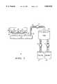
- FIG. 1illustrates a partial schematic view of a chemical-mechanical polishing tool in accordance with the present invention
- FIG. 2outlines a method of chemically-mechanically polishing a substrate in accordance with the present invention.
- FIG. 1illustrates a partial schematic view of a chemical-mechanical polishing (CMP) tool 10 that includes a dispensing tube 12 for dispensing a slurry 28 onto a polishing pad 11.
- a pump 13extracts or pumps slurry 28 from a mixing or holding tank 14 into tube 12, and pumps 15 and 16 extract a colloid 17 and a reagent 18, respectively, into tank 14 to form slurry 28.
- tank 14is not used in tool 10.
- an in-line mixeras known in the art, is used in place of tank 14, and the use of pump 13 is optional.
- Colloid 17has a degree of acidity or basicity (i.e., a pH value or level) of approximately 1-12.
- Colloid 17also includes abrasive particles typically comprises alumina or silica that are held in suspension within colloid 17.
- SC-112which is a colloid containing silica particles
- WA335which is a colloid containing alumina particles
- Reagent 18is described in more detail hereinafter.
- a substrate 19is processed by tool 10.
- Substrate 19can comprise a semiconductor layer 21 that supports an electrically insulative layer 22 and an electrically conductive layer 23, which can comprise a dielectric layer and a metal layer, respectively.
- layers 21 and 22can comprise silicon and silicon oxide, respectively, and layer 23 can comprise aluminum, copper, tungsten, tantalum, tantalum nitride, titanium, or titanium nitride.
- Layer 22has trenches or vias 26 and 27 in which a portion of layer 23 is located.
- a surface 24 of substrate 19comprise a portion of layers 22 and 23.
- Slurry 28should have appropriate polishing selectivities for layers 22 and 23 in order for the CMP process to produce a substantially planar surface for substrate 19. Accordingly, the polishing rate for layer 23 should be significantly higher than the polishing rate for layer 22.
- Reagent 18can provide the preferred polishing selectivities while substantially maintaining or balancing the colloidal, electrochemical, and rheological properties in slurry 28. Reagent 18 can also be used to inhibit the corrosion of electrically conductive layer 23 during the CMP process as described hereinafter. Suitable materials for reagent 18 are discussed hereinafter.
- Reagent 18can also be used to extend the lifetime of pad 11 and to improve the uniformity of the CMP process.
- Pad 11typically has grooves, holes, or pores to improve the transport efficiency of slurry 28 across pad 11 because the same portion of slurry 28 should not remain between pad 11 and substrate 19 in order to ensure a uniform polishing of substrate 19.
- particles or by-products of the CMP processoften clog the grooves, holes, or pores, which degrade the even distribution or transport of slurry 28 across pad 11, and thus, the quality of the CMP process is detrimentally affected.
- Reagent 18can be used to passivate or protect the grooves, holes, or pores from becoming clogged while still permitting the grooves, holes, or pores to enhance the transport of slurry 28, as explained hereinafter. By preventing the grooves, holes, or pores from being clogged, reagent 18 extends the lifetime of pad 11 and also reduces the amount of maintenance required to condition or replace pad 11.
- reagent 18By using reagent 18 to accomplish all of the improvements described above, the colloidal properties of slurry 28 are not detrimentally degraded by the addition of too many additives. Consequently, the colloidal properties, the electro-chemical properties, the selectivities, and the pH value of slurry 28 are more easily maintained and controlled. Clearly, the use of reagent 18 provides distinct advantages over the prior art.
- FIG. 2outlines a method 50 of chemically-mechanically polishing a substrate.
- Method 50is described in relationship to fabricating a component or manufacturing a semiconductor device as previously described in FIG. 1.
- a substratesuch as, for example, substrate 19 of FIG. 1 that has layers 22 and 23 is provided in a step 51 of method 50.
- a step 52 of method 50provides a mixture having particles or a colloid such as, for example, colloid 17 of FIG. 1, and a step 53 of method 50 provides a reagent or an additive such as, for example, reagent 18 of FIG. 1.
- Suitable reagents for step 53include, but are not limited to, organic salts that are either chelated or non-chelated and that are either cationic or anionic.
- organic saltsthat are either chelated or non-chelated and that are either cationic or anionic.
- non-chelated organic saltthat is cationic include, but are not limited to, tetramethylammonium iodate ((CH 3 ) 4 NIO 3 ), tetramethylammonium periodate ((CH 3 ) 4 NIO 4 ), tetramethylammonium nitrate ((CH 3 ) 4 N + NO 3 - ), tetraethylammonium nitrate ((C 2 H 5 ) 4 N + NO 3 - ), tetramethylammonium sulfate ((C 3 ) 4 N + SO 4 - ) tetraethylammonium sulfate ((C 2 H 5 ) 4 N + SO 4 - ), and bistetramethylammonium persulfate ((CH 3 ) 4 N ++ S 2 O 8 - ).
- Non-chelated organic salt that is anionicincludes, but is not limited to, ammonium methylsulfate (NH 4 + CH 3 SO 3 - ).
- Reagent 18can alternatively comprise a non-chelated cationic or anionic organic salt that includes a transition metal such as, for example, tetramethylammonium iron sulfate (N(CH 3 ) 4 Fe(SO 4 ) 2 ), tetramethylammonium cerium nitrate (N(CH 3 ) 4 Ce(NO 3 ) 6 ), tetramethylammonium cerium sulfate (N(CH 3 ) 4 Ce(SO 4 ) 4 ), tetramethylammonium aluminum sulfate (N(CH 3 ) 4 Al(SO 4 ) 4 ), tetramethylammonium aluminum nitrate ((N(CH 3 ) 4 Al(NO 3 ) 3 ), ammonium iron methylsulfate (NH 4 FeCH 3 SO 3 - -
- a step 54 of method 50disposes or positions substrate 19 in a processing tool such as, for example, CMP tool 10 of FIG. 1. Then, the mixture or colloid of step 52 is combined or mixed with the reagent or organic salt of step 53 during a step 55, which forms a slurry such as, for example, slurry 28 of FIG. 1.
- the slurrymay comprise a weight ratio of approximately 10:1 to 100:1 between the colloid and the organic salt.
- Step 55can be performed prior to or during a subsequent step 57 described hereinafter.
- the reagent or organic saltis broken apart or separated apart into at least two reaction products or, more specifically, the reagent is decomposed into an oxidizer and a surfactant.
- an oxidizer and a surfactantAs known in the art of CMP, it is common practice to refer to the oxidizer as an etchant, especially when the CMP process is applied to a layer comprising aluminum or copper.
- the term "oxidizer”is used interchangeably with the term "etchant.”
- the oxidizer and the surfactantcan both be organic components, or the reaction products can comprise an organic component and an inorganic component.
- the organic saltcan decompose into an organic component of tetramethylammonium hydroxide (TMAH) and an inorganic component of aluminum nitrate during step 56.
- TMAHtetramethylammonium hydroxide
- the aluminum nitrateis an oxidizer that can improve the polishing rate of layer 23.
- the TMAHis a surfactant that passivates layer 22 of substrate 19 using a mechanism known in the art as steric hindrance or shielding to improve the selectivity of the slurry.
- the polishing rate of layer 23is increased; the polishing rate of layer 22 is reduced; and the polishing selectivity of the slurry is improved.
- the TMAHalso passivates polishing pad 11 and prevents the grooves, holes, or pores of pad 11 from being clogged by modifying interfacial forces between the slurry, pad 11, and substrate 19. Therefore, the lifetime of pad 11 is extended, and the transport efficiency of the slurry is not degraded. Consequently, process stability is improved, and the across-wafer and wafer-to-wafer non-uniformities are reduced. Furthermore, the TMAH is a corrosion inhibitor for electrically conductive layer 23 when layer 23 comprise aluminum.
- the TMAHis not directly added to the colloid because the TMAH is basic and would significantly and detrimentally alter the pH level of the colloid and severely degrade the slurry transport, the rheological properties of the slurry, and many other aspects of the CMP process.
- the addition of tetramethylammonium aluminum nitratedoes not detrimentally alter the stability of the colloid because tetramethylammonium aluminum nitrate is in a salt form that includes compensated counter ions.
- the changes in the pH level associated with the addition of the tetramethylammonium aluminum nitratestill provide a stable colloidal suspension.
- the TMAH and aluminum nitrateare not individually added or combined with the colloid because of difficulties in obtaining a balanced pH level while mixing the TMAH and the aluminum nitrate with the colloid.
- the difficulties associated with maintaining a balanced pH levelare alleviated when a salt, which has compensated counter ions, is mixed with the colloid. Therefore, a single reagent of tetramethylammonium aluminum nitrate is added to the colloid to provide the advantages discussed above without detrimentally affecting the colloidal, electrochemical, or Theological properties of the slurry.
- the slurry of step 55preferably consists essentially of the colloid and the organic salt and preferably does not contain other additives.
- the decomposition of the organic saltimproves many aspects of the polishing performance of the slurry without degrading other aspects of the CMP process.
- the slurry of step 55is used to process substrate 19 in the CMP tool by applying the colloid and the reagent or organic salt to substrate 19 to chemically and mechanically polish substrate 19 during a step 57.
- substrate 19is removed from the CMP tool during a step 58.
- the physical or chemical reaction of the organic salt with a metalserves as a catalyst for the decomposition of the organic salt in step 56.
- the metalcould include an exposed metal within the electrically conductive layer 23 of substrate 19, or polishing product on the polishing pad 11 (FIG. 1). Additional heat can be supplied during step 57 to further promote the decomposition of the organic salt. Additional heat or increased down force pressure during step 57 can be provided during polishing.
- steps 55 and 56can occur during step 57 by using point-of-use mixing.
- the organic saltpreferably does not decompose during steps 52, 53, or 55 so that the colloidal properties and the pH value of the slurry are not degraded prior to using the slurry in step 57.
- the electrically conductive layer 23is a copper layer
- the electrically insulative layeris an oxide layer.
- the substrate 19 including the copper and oxide layersis polished using a slurry formulation that includes a non-chelated organic salt that forms tetramethylammonium sulfate cations.
- the copper polishing rateis in a range of approximately 4000-6000 angstroms per minute, and the selectivity is in a range of approximately 100:1 to 200:1 (angstroms of copper polished for each angstrom of oxide polished.)
- an improved slurry for chemically-mechanically polishing a metal layerthat overcomes the disadvantages of the prior art.
- the use of fewer reagents in the slurrycan simultaneously provide all of the previously described improvements over conventional slurries wherein the improvements include, but are not limited to, improving polishing selectivity, preventing metal corrosion during polishing, improving slurry transport efficiency, and extending the lifetime of a polishing pad.
- the use of fewer reagents instead of a large plurality of reagentsreduces the cost of the CMP process, stabilizes the colloid, and simplifies the CMP process.
- the colloidal, electrochemical, and rheological properties of the slurryare not significantly distorted because fewer reagents are added compared to the prior art.
Landscapes
- Engineering & Computer Science (AREA)
- Chemical & Material Sciences (AREA)
- Computer Hardware Design (AREA)
- Microelectronics & Electronic Packaging (AREA)
- Power Engineering (AREA)
- General Chemical & Material Sciences (AREA)
- Chemical Kinetics & Catalysis (AREA)
- Materials Engineering (AREA)
- Mechanical Engineering (AREA)
- Metallurgy (AREA)
- Organic Chemistry (AREA)
- Mechanical Treatment Of Semiconductor (AREA)
- Grinding And Polishing Of Tertiary Curved Surfaces And Surfaces With Complex Shapes (AREA)
Abstract
Description
Claims (19)
Priority Applications (2)
| Application Number | Priority Date | Filing Date | Title |
|---|---|---|---|
| US08/684,782US5863838A (en) | 1996-07-22 | 1996-07-22 | Method for chemically-mechanically polishing a metal layer |
| JP20847197AJP3977901B2 (en) | 1996-07-22 | 1997-07-16 | Device manufacturing method |
Applications Claiming Priority (1)
| Application Number | Priority Date | Filing Date | Title |
|---|---|---|---|
| US08/684,782US5863838A (en) | 1996-07-22 | 1996-07-22 | Method for chemically-mechanically polishing a metal layer |
Publications (1)
| Publication Number | Publication Date |
|---|---|
| US5863838Atrue US5863838A (en) | 1999-01-26 |
Family
ID=24749548
Family Applications (1)
| Application Number | Title | Priority Date | Filing Date |
|---|---|---|---|
| US08/684,782Expired - LifetimeUS5863838A (en) | 1996-07-22 | 1996-07-22 | Method for chemically-mechanically polishing a metal layer |
Country Status (2)
| Country | Link |
|---|---|
| US (1) | US5863838A (en) |
| JP (1) | JP3977901B2 (en) |
Cited By (29)
| Publication number | Priority date | Publication date | Assignee | Title |
|---|---|---|---|---|
| US6048256A (en)* | 1999-04-06 | 2000-04-11 | Lucent Technologies Inc. | Apparatus and method for continuous delivery and conditioning of a polishing slurry |
| US6096652A (en)* | 1997-11-03 | 2000-08-01 | Motorola, Inc. | Method of chemical mechanical planarization using copper coordinating ligands |
| US6130163A (en)* | 1999-06-03 | 2000-10-10 | Promos Technologies, Inc. | Stabilization of slurry used in chemical mechanical polishing of semiconductor wafers by adjustment of PH of deionized water |
| WO2000060917A3 (en)* | 1999-04-09 | 2001-01-11 | Micron Technology Inc | Bi-modal abrasive slurries for planarization |
| US6316365B1 (en)* | 1999-12-07 | 2001-11-13 | Cabot Microelectronics Corporation | Chemical-mechanical polishing method |
| US6332831B1 (en)* | 2000-04-06 | 2001-12-25 | Fujimi America Inc. | Polishing composition and method for producing a memory hard disk |
| US6383414B1 (en)* | 1997-08-26 | 2002-05-07 | Lsi Logic Corporation | Use of corrosion inhibiting compounds to inhibit corrosion of metal plugs in chemical-mechanical polishing |
| US6402884B1 (en)* | 1999-04-09 | 2002-06-11 | Micron Technology, Inc. | Planarizing solutions, planarizing machines and methods for mechanical or chemical-mechanical planarization of microelectronic-device substrate assemblies |
| US6419554B2 (en)* | 1999-06-24 | 2002-07-16 | Micron Technology, Inc. | Fixed abrasive chemical-mechanical planarization of titanium nitride |
| US6431950B1 (en)* | 2000-10-18 | 2002-08-13 | Micron Technology, Inc. | Point-of-use fluid regulating system for use in the chemical-mechanical planarization of semiconductor wafers |
| US6461965B1 (en)* | 2002-01-31 | 2002-10-08 | Texas Instruments Incorporated | Method for effecting a finishing operation on a semiconductor workpiece |
| US20030216049A1 (en)* | 2000-12-01 | 2003-11-20 | Applied Materials, Inc. | Method and composition for the removal of residual materials during substrate planarization |
| US6689692B1 (en)* | 1996-12-30 | 2004-02-10 | Cabot Microelectronics Corporation | Composition for oxide CMP |
| US6783432B2 (en) | 2001-06-04 | 2004-08-31 | Applied Materials Inc. | Additives for pressure sensitive polishing compositions |
| US6821187B2 (en) | 2000-09-29 | 2004-11-23 | Infineon Technologies Ag | Method for chemical-mechanical polishing of a layer which is a substrate and is a metal selected from a platinum group |
| US20040244911A1 (en)* | 2001-08-09 | 2004-12-09 | Lee Jae Seok | Sluury composition for use in chemical mechanical polishing of metal wiring |
| US20040259366A1 (en)* | 2003-06-20 | 2004-12-23 | Kim Seong Han | Method and composition for the chemical-vibrational-mechanical planarization of copper |
| US20050031789A1 (en)* | 2003-08-05 | 2005-02-10 | Zhendong Liu | Composition for polishing semiconductor layers |
| US20050062016A1 (en)* | 2001-08-09 | 2005-03-24 | Lee Jae Seok | Metal CMP slurry compositions that favor mechanical removal of metal oxides with reduced susceptibility to micro-scratching |
| US20050072524A1 (en)* | 2000-04-11 | 2005-04-07 | Cabot Microelectronics Corporation | System for the preferential removal of silicon oxide |
| US20050236601A1 (en)* | 2004-04-21 | 2005-10-27 | Zhendong Liu | Barrier polishing solution |
| US20060110923A1 (en)* | 2004-11-24 | 2006-05-25 | Zhendong Liu | Barrier polishing solution |
| US20070010098A1 (en)* | 2005-06-30 | 2007-01-11 | Cabot Microelectronics Corporation | Use of CMP for aluminum mirror and solar cell fabrication |
| RU2292679C2 (en)* | 2005-02-18 | 2007-01-27 | Закрытое акционерное общество "Элма-Фотма" | Method for making photo-template blanks |
| US20080287041A1 (en)* | 2005-11-08 | 2008-11-20 | Freescale Semiconductor, Inc. | System and Method for Removing Particles From a Polishing Pad |
| US20080311834A1 (en)* | 2005-10-19 | 2008-12-18 | Freescale Semiconductor. Inc. | System and Method for Cleaning a Conditioning Device |
| EP2048208A2 (en) | 2002-02-11 | 2009-04-15 | DuPont Air Products NanoMaterials L.L.C. | Free radical-forming activator attached to solid and used to enhanced CMP formulations |
| EP3597711A1 (en) | 2018-07-20 | 2020-01-22 | Versum Materials US, LLC | Tungsten chemical mechanical polishing for reduced oxide erosion |
| US10570313B2 (en) | 2015-02-12 | 2020-02-25 | Versum Materials Us, Llc | Dishing reducing in tungsten chemical mechanical polishing |
Families Citing this family (2)
| Publication number | Priority date | Publication date | Assignee | Title |
|---|---|---|---|---|
| JP4816836B2 (en)* | 1998-12-28 | 2011-11-16 | 日立化成工業株式会社 | Polishing liquid for metal and polishing method using the same |
| CN104131292B (en)* | 2014-07-01 | 2015-10-28 | 蚌埠市高华电子有限公司 | Etch-proof composite polishing liquid of a kind of easy to clean and preparation method thereof |
Citations (5)
| Publication number | Priority date | Publication date | Assignee | Title |
|---|---|---|---|---|
| US5084071A (en)* | 1989-03-07 | 1992-01-28 | International Business Machines Corporation | Method of chemical-mechanical polishing an electronic component substrate and polishing slurry therefor |
| US5139571A (en)* | 1991-04-24 | 1992-08-18 | Motorola, Inc. | Non-contaminating wafer polishing slurry |
| US5225034A (en)* | 1992-06-04 | 1993-07-06 | Micron Technology, Inc. | Method of chemical mechanical polishing predominantly copper containing metal layers in semiconductor processing |
| US5391258A (en)* | 1993-05-26 | 1995-02-21 | Rodel, Inc. | Compositions and methods for polishing |
| US5527423A (en)* | 1994-10-06 | 1996-06-18 | Cabot Corporation | Chemical mechanical polishing slurry for metal layers |
- 1996
- 1996-07-22USUS08/684,782patent/US5863838A/ennot_activeExpired - Lifetime
- 1997
- 1997-07-16JPJP20847197Apatent/JP3977901B2/ennot_activeExpired - Fee Related
Patent Citations (5)
| Publication number | Priority date | Publication date | Assignee | Title |
|---|---|---|---|---|
| US5084071A (en)* | 1989-03-07 | 1992-01-28 | International Business Machines Corporation | Method of chemical-mechanical polishing an electronic component substrate and polishing slurry therefor |
| US5139571A (en)* | 1991-04-24 | 1992-08-18 | Motorola, Inc. | Non-contaminating wafer polishing slurry |
| US5225034A (en)* | 1992-06-04 | 1993-07-06 | Micron Technology, Inc. | Method of chemical mechanical polishing predominantly copper containing metal layers in semiconductor processing |
| US5391258A (en)* | 1993-05-26 | 1995-02-21 | Rodel, Inc. | Compositions and methods for polishing |
| US5527423A (en)* | 1994-10-06 | 1996-06-18 | Cabot Corporation | Chemical mechanical polishing slurry for metal layers |
Non-Patent Citations (6)
| Title |
|---|
| F.B.Kaufman, et al., "Chemical-Mechanical Polishing for Fabricating Patterned W Metal Features as Chip Interconnects", J.Electrochem, Soc., vol. 138, No. 11, Nov. 1991, pp. 3460-3465. |
| F.B.Kaufman, et al., Chemical Mechanical Polishing for Fabricating Patterned W Metal Features as Chip Interconnects , J.Electrochem, Soc., vol. 138, No. 11, Nov. 1991, pp. 3460 3465.* |
| Ronald Carpio, et al., "Initial study on copper CMP slurry chemistries", Sematech, Thin Solid Films 266 (1995), pp. 238-244. |
| Ronald Carpio, et al., Initial study on copper CMP slurry chemistries , Sematech, Thin Solid Films 266 (1995), pp. 238 244.* |
| S.P.Muraka, et al., "Advanced Metallization for Devices and Circuits--Science, Technology and Manufacturability", Mat.,Res.Soc.Symp.Proc., vol. 337, Apr. 4-8, 1994, pp. 133-138. |
| S.P.Muraka, et al., Advanced Metallization for Devices and Circuits Science, Technology and Manufacturability , Mat.,Res.Soc.Symp.Proc., vol. 337, Apr. 4 8, 1994, pp. 133 138.* |
Cited By (62)
| Publication number | Priority date | Publication date | Assignee | Title |
|---|---|---|---|---|
| US6984588B2 (en)* | 1996-12-30 | 2006-01-10 | Cabot Microelectronics Corporation | Compositions for oxide CMP |
| US20040089634A1 (en)* | 1996-12-30 | 2004-05-13 | Cabot Microelectronics Corporation | Compositions for oxide CMP |
| US6689692B1 (en)* | 1996-12-30 | 2004-02-10 | Cabot Microelectronics Corporation | Composition for oxide CMP |
| US6383414B1 (en)* | 1997-08-26 | 2002-05-07 | Lsi Logic Corporation | Use of corrosion inhibiting compounds to inhibit corrosion of metal plugs in chemical-mechanical polishing |
| US6096652A (en)* | 1997-11-03 | 2000-08-01 | Motorola, Inc. | Method of chemical mechanical planarization using copper coordinating ligands |
| US6048256A (en)* | 1999-04-06 | 2000-04-11 | Lucent Technologies Inc. | Apparatus and method for continuous delivery and conditioning of a polishing slurry |
| US6407000B1 (en) | 1999-04-09 | 2002-06-18 | Micron Technology, Inc. | Method and apparatuses for making and using bi-modal abrasive slurries for mechanical and chemical-mechanical planarization of microelectronic-device substrate assemblies |
| WO2000060917A3 (en)* | 1999-04-09 | 2001-01-11 | Micron Technology Inc | Bi-modal abrasive slurries for planarization |
| US7122475B2 (en) | 1999-04-09 | 2006-10-17 | Micron Technology, Inc. | Methods for using bi-modal abrasive slurries for mechanical and chemical-mechanical planarization of microelectronic-device substrate assemblies |
| US20040229551A1 (en)* | 1999-04-09 | 2004-11-18 | Hudson Guy F. | Systems for making and using bi-modal abrasive slurries for mechanical and chemical-mechanical planarization of microelectronic-device substrate assemblies |
| US6805615B1 (en) | 1999-04-09 | 2004-10-19 | Micron Technology, Inc. | Planarizing solutions, planarizing machines and methods for mechanical or chemical-mechanical planarization of microelectronic-device substrate assemblies |
| US20040198194A1 (en)* | 1999-04-09 | 2004-10-07 | Hudson Guy F. | Methods for using bi-modal abrasive slurries for mechanical and chemical-mechanical planarization of microelectronic-device substrate assemblies |
| US20050107010A1 (en)* | 1999-04-09 | 2005-05-19 | Robinson Karl M. | Planarizing solutions, planarizing machines and methods for mechanical or chemical-mechanical planarization of microelectronic-device substrate assemblies |
| US6599836B1 (en)* | 1999-04-09 | 2003-07-29 | Micron Technology, Inc. | Planarizing solutions, planarizing machines and methods for mechanical or chemical-mechanical planarization of microelectronic-device substrate assemblies |
| US7276446B2 (en) | 1999-04-09 | 2007-10-02 | Micron Technology, Inc. | Planarizing solutions, planarizing machines and methods for mechanical or chemical-mechanical planarization of microelectronic-device substrate assemblies |
| US20040198195A1 (en)* | 1999-04-09 | 2004-10-07 | Hudson Guy F. | Apparatuses for making and using bi-modal abrasive slurries for mechanical and chemical-mechanical planarization of microelectronic-device substrate assemblies |
| US6794289B2 (en) | 1999-04-09 | 2004-09-21 | Micron Technology, Inc. | Method and apparatuses for making and using bi-modal abrasive slurries for mechanical and chemical-mechanical planarization of microelectronic-device substrate assemblies |
| US6402884B1 (en)* | 1999-04-09 | 2002-06-11 | Micron Technology, Inc. | Planarizing solutions, planarizing machines and methods for mechanical or chemical-mechanical planarization of microelectronic-device substrate assemblies |
| US6130163A (en)* | 1999-06-03 | 2000-10-10 | Promos Technologies, Inc. | Stabilization of slurry used in chemical mechanical polishing of semiconductor wafers by adjustment of PH of deionized water |
| US6881129B2 (en) | 1999-06-24 | 2005-04-19 | Micron Technology, Inc. | Fixed-abrasive chemical-mechanical planarization of titanium nitride |
| US7402094B2 (en) | 1999-06-24 | 2008-07-22 | Micron Technology, Inc. | Fixed-abrasive chemical-mechanical planarization of titanium nitride |
| US20020106977A1 (en)* | 1999-06-24 | 2002-08-08 | Micron Technology, Inc. | Fixed-abrasive chemical-mechanical planarization of titanium nitride |
| US6419554B2 (en)* | 1999-06-24 | 2002-07-16 | Micron Technology, Inc. | Fixed abrasive chemical-mechanical planarization of titanium nitride |
| US20060003675A1 (en)* | 1999-06-24 | 2006-01-05 | Micron Technology, Inc. | Fixed-abrasive chemical-mechanical planarization of titanium nitride |
| US20050199588A1 (en)* | 1999-06-24 | 2005-09-15 | Micron Technology, Inc. | Fixed-abrasive chemical-mechanical planarization of titanium nitride |
| US6997781B2 (en) | 1999-06-24 | 2006-02-14 | Micron Technology, Inc. | Fixed-abrasive chemical-mechanical planarization of titanium nitride |
| US6316365B1 (en)* | 1999-12-07 | 2001-11-13 | Cabot Microelectronics Corporation | Chemical-mechanical polishing method |
| US6332831B1 (en)* | 2000-04-06 | 2001-12-25 | Fujimi America Inc. | Polishing composition and method for producing a memory hard disk |
| US20070120090A1 (en)* | 2000-04-11 | 2007-05-31 | Cabot Microelectronics Corporation | System for the Preferential Removal of Silicon Oxide |
| US20050072524A1 (en)* | 2000-04-11 | 2005-04-07 | Cabot Microelectronics Corporation | System for the preferential removal of silicon oxide |
| US7238618B2 (en) | 2000-04-11 | 2007-07-03 | Cabot Microelectronics Corporation | System for the preferential removal of silicon oxide |
| US7365013B2 (en) | 2000-04-11 | 2008-04-29 | Cabot Microelectronics Corporation | System for the preferential removal of silicon oxide |
| US6821187B2 (en) | 2000-09-29 | 2004-11-23 | Infineon Technologies Ag | Method for chemical-mechanical polishing of a layer which is a substrate and is a metal selected from a platinum group |
| US6656015B2 (en) | 2000-10-18 | 2003-12-02 | Micron Technology, Inc. | Point-of-use fluid regulating system for use in the chemical-mechanical planarization of semiconductor wafers |
| US6764378B2 (en) | 2000-10-18 | 2004-07-20 | Micron Technology, Inc. | Point-of-use fluid regulating system for use in the chemical-mechanical planarization of semiconductor wafers |
| US6431950B1 (en)* | 2000-10-18 | 2002-08-13 | Micron Technology, Inc. | Point-of-use fluid regulating system for use in the chemical-mechanical planarization of semiconductor wafers |
| US20030216049A1 (en)* | 2000-12-01 | 2003-11-20 | Applied Materials, Inc. | Method and composition for the removal of residual materials during substrate planarization |
| US7022608B2 (en) | 2000-12-01 | 2006-04-04 | Applied Materials Inc. | Method and composition for the removal of residual materials during substrate planarization |
| US6783432B2 (en) | 2001-06-04 | 2004-08-31 | Applied Materials Inc. | Additives for pressure sensitive polishing compositions |
| US6953389B2 (en) | 2001-08-09 | 2005-10-11 | Cheil Industries, Inc. | Metal CMP slurry compositions that favor mechanical removal of oxides with reduced susceptibility to micro-scratching |
| US20050227491A1 (en)* | 2001-08-09 | 2005-10-13 | Lee Jae S | Methods of forming integrated circuit devices having polished tungsten metal layers therein |
| US20050062016A1 (en)* | 2001-08-09 | 2005-03-24 | Lee Jae Seok | Metal CMP slurry compositions that favor mechanical removal of metal oxides with reduced susceptibility to micro-scratching |
| US7452815B2 (en) | 2001-08-09 | 2008-11-18 | Cheil Industries, Inc. | Methods of forming integrated circuit devices having polished tungsten metal layers therein |
| US6930054B2 (en) | 2001-08-09 | 2005-08-16 | Cheil Industries, Inc. | Slurry composition for use in chemical mechanical polishing of metal wiring |
| US20040244911A1 (en)* | 2001-08-09 | 2004-12-09 | Lee Jae Seok | Sluury composition for use in chemical mechanical polishing of metal wiring |
| US6461965B1 (en)* | 2002-01-31 | 2002-10-08 | Texas Instruments Incorporated | Method for effecting a finishing operation on a semiconductor workpiece |
| EP2048208A2 (en) | 2002-02-11 | 2009-04-15 | DuPont Air Products NanoMaterials L.L.C. | Free radical-forming activator attached to solid and used to enhanced CMP formulations |
| US20040259366A1 (en)* | 2003-06-20 | 2004-12-23 | Kim Seong Han | Method and composition for the chemical-vibrational-mechanical planarization of copper |
| US7018560B2 (en) | 2003-08-05 | 2006-03-28 | Rohm And Haas Electronic Materials Cmp Holdings, Inc. | Composition for polishing semiconductor layers |
| US20050031789A1 (en)* | 2003-08-05 | 2005-02-10 | Zhendong Liu | Composition for polishing semiconductor layers |
| US20050236601A1 (en)* | 2004-04-21 | 2005-10-27 | Zhendong Liu | Barrier polishing solution |
| US7253111B2 (en) | 2004-04-21 | 2007-08-07 | Rohm And Haas Electronic Materials Cmp Holding, Inc. | Barrier polishing solution |
| US20060110923A1 (en)* | 2004-11-24 | 2006-05-25 | Zhendong Liu | Barrier polishing solution |
| RU2292679C2 (en)* | 2005-02-18 | 2007-01-27 | Закрытое акционерное общество "Элма-Фотма" | Method for making photo-template blanks |
| US8062096B2 (en) | 2005-06-30 | 2011-11-22 | Cabot Microelectronics Corporation | Use of CMP for aluminum mirror and solar cell fabrication |
| US20070010098A1 (en)* | 2005-06-30 | 2007-01-11 | Cabot Microelectronics Corporation | Use of CMP for aluminum mirror and solar cell fabrication |
| US20080311834A1 (en)* | 2005-10-19 | 2008-12-18 | Freescale Semiconductor. Inc. | System and Method for Cleaning a Conditioning Device |
| US8545634B2 (en) | 2005-10-19 | 2013-10-01 | Freescale Semiconductor, Inc. | System and method for cleaning a conditioning device |
| US20080287041A1 (en)* | 2005-11-08 | 2008-11-20 | Freescale Semiconductor, Inc. | System and Method for Removing Particles From a Polishing Pad |
| US7883393B2 (en)* | 2005-11-08 | 2011-02-08 | Freescale Semiconductor, Inc. | System and method for removing particles from a polishing pad |
| US10570313B2 (en) | 2015-02-12 | 2020-02-25 | Versum Materials Us, Llc | Dishing reducing in tungsten chemical mechanical polishing |
| EP3597711A1 (en) | 2018-07-20 | 2020-01-22 | Versum Materials US, LLC | Tungsten chemical mechanical polishing for reduced oxide erosion |
Also Published As
| Publication number | Publication date |
|---|---|
| JP3977901B2 (en) | 2007-09-19 |
| JPH1074719A (en) | 1998-03-17 |
Similar Documents
| Publication | Publication Date | Title |
|---|---|---|
| US5863838A (en) | Method for chemically-mechanically polishing a metal layer | |
| EP0971993B1 (en) | Planarization composition for removing metal films | |
| KR100690470B1 (en) | Mechanochemical Polishing of Copper Substrates | |
| EP2431434B1 (en) | Polishing Composition for Noble Metals | |
| EP0706582B2 (en) | Improved compositions and methods for polishing | |
| US7153335B2 (en) | Tunable composition and method for chemical-mechanical planarization with aspartic acid/tolyltriazole | |
| US6077337A (en) | Chemical-mechanical polishing slurry | |
| US10160884B2 (en) | Metal compound chemically anchored colloidal particles and methods of production and use thereof | |
| US7429338B2 (en) | Surface modified colloidal abrasives, including stable bimetallic surface coated silica sols for chemical mechanical planarization | |
| EP2321378B1 (en) | Chemical-mechanical polishing compositions and methods of making and using the same | |
| KR19990063753A (en) | Chemical mechanical polishing compositions and chemical mechanical polishing methods | |
| KR19980042755A (en) | Compositions and slurries useful for chemical mechanical polishing of metals | |
| US20130045598A1 (en) | Method for chemical mechanical polishing tungsten | |
| EP1489650B1 (en) | Polishing composition and method for forming wiring structure | |
| US6719920B2 (en) | Slurry for polishing a barrier layer | |
| US20010052587A1 (en) | Chemical mechanical polishing slurry and method for polishing metal/oxide layers | |
| KR20140014332A (en) | A stabilized, concentratable chemical mechanical polishing composition and method of polishing a substrate | |
| WO2008022277A2 (en) | Selective chemistry for fixed abrasive cmp | |
| CN113874464A (en) | Polishing liquid, dispersion, method for producing polishing liquid, and polishing method | |
| KR20230044961A (en) | Method of enhancing the removal rate of polysilicon | |
| US6440857B1 (en) | Two-step CMP method and employed polishing compositions | |
| US20020053656A1 (en) | Ceric-ion slurry for use in chemical-mechanical polishing | |
| US6693035B1 (en) | Methods to control film removal rates for improved polishing in metal CMP | |
| KR100479804B1 (en) | Slurry compositions for metal cmp | |
| EP1928964B1 (en) | Composition and method for planarizing surfaces |
Legal Events
| Date | Code | Title | Description |
|---|---|---|---|
| AS | Assignment | Owner name:MOTOROLA, INC., ILLINOIS Free format text:ASSIGNMENT OF ASSIGNORS INTEREST;ASSIGNORS:FARKAS, JANOS;FREEMAN, MELISSA;REEL/FRAME:008114/0352 Effective date:19960718 | |
| STCF | Information on status: patent grant | Free format text:PATENTED CASE | |
| FPAY | Fee payment | Year of fee payment:4 | |
| AS | Assignment | Owner name:FREESCALE SEMICONDUCTOR, INC., TEXAS Free format text:ASSIGNMENT OF ASSIGNORS INTEREST;ASSIGNOR:MOTOROLA, INC.;REEL/FRAME:015698/0657 Effective date:20040404 Owner name:FREESCALE SEMICONDUCTOR, INC.,TEXAS Free format text:ASSIGNMENT OF ASSIGNORS INTEREST;ASSIGNOR:MOTOROLA, INC.;REEL/FRAME:015698/0657 Effective date:20040404 | |
| FPAY | Fee payment | Year of fee payment:8 | |
| AS | Assignment | Owner name:CITIBANK, N.A. AS COLLATERAL AGENT, NEW YORK Free format text:SECURITY AGREEMENT;ASSIGNORS:FREESCALE SEMICONDUCTOR, INC.;FREESCALE ACQUISITION CORPORATION;FREESCALE ACQUISITION HOLDINGS CORP.;AND OTHERS;REEL/FRAME:018855/0129 Effective date:20061201 Owner name:CITIBANK, N.A. AS COLLATERAL AGENT,NEW YORK Free format text:SECURITY AGREEMENT;ASSIGNORS:FREESCALE SEMICONDUCTOR, INC.;FREESCALE ACQUISITION CORPORATION;FREESCALE ACQUISITION HOLDINGS CORP.;AND OTHERS;REEL/FRAME:018855/0129 Effective date:20061201 | |
| AS | Assignment | Owner name:CITIBANK, N.A., AS COLLATERAL AGENT,NEW YORK Free format text:SECURITY AGREEMENT;ASSIGNOR:FREESCALE SEMICONDUCTOR, INC.;REEL/FRAME:024397/0001 Effective date:20100413 Owner name:CITIBANK, N.A., AS COLLATERAL AGENT, NEW YORK Free format text:SECURITY AGREEMENT;ASSIGNOR:FREESCALE SEMICONDUCTOR, INC.;REEL/FRAME:024397/0001 Effective date:20100413 | |
| FPAY | Fee payment | Year of fee payment:12 | |
| AS | Assignment | Owner name:CITIBANK, N.A., AS NOTES COLLATERAL AGENT, NEW YORK Free format text:SECURITY AGREEMENT;ASSIGNOR:FREESCALE SEMICONDUCTOR, INC.;REEL/FRAME:030633/0424 Effective date:20130521 Owner name:CITIBANK, N.A., AS NOTES COLLATERAL AGENT, NEW YOR Free format text:SECURITY AGREEMENT;ASSIGNOR:FREESCALE SEMICONDUCTOR, INC.;REEL/FRAME:030633/0424 Effective date:20130521 | |
| AS | Assignment | Owner name:CITIBANK, N.A., AS NOTES COLLATERAL AGENT, NEW YORK Free format text:SECURITY AGREEMENT;ASSIGNOR:FREESCALE SEMICONDUCTOR, INC.;REEL/FRAME:031591/0266 Effective date:20131101 Owner name:CITIBANK, N.A., AS NOTES COLLATERAL AGENT, NEW YOR Free format text:SECURITY AGREEMENT;ASSIGNOR:FREESCALE SEMICONDUCTOR, INC.;REEL/FRAME:031591/0266 Effective date:20131101 | |
| AS | Assignment | Owner name:FREESCALE SEMICONDUCTOR, INC., TEXAS Free format text:PATENT RELEASE;ASSIGNOR:CITIBANK, N.A., AS COLLATERAL AGENT;REEL/FRAME:037356/0553 Effective date:20151207 Owner name:FREESCALE SEMICONDUCTOR, INC., TEXAS Free format text:PATENT RELEASE;ASSIGNOR:CITIBANK, N.A., AS COLLATERAL AGENT;REEL/FRAME:037354/0225 Effective date:20151207 Owner name:FREESCALE SEMICONDUCTOR, INC., TEXAS Free format text:PATENT RELEASE;ASSIGNOR:CITIBANK, N.A., AS COLLATERAL AGENT;REEL/FRAME:037356/0143 Effective date:20151207 | |
| AS | Assignment | Owner name:MORGAN STANLEY SENIOR FUNDING, INC., MARYLAND Free format text:ASSIGNMENT AND ASSUMPTION OF SECURITY INTEREST IN PATENTS;ASSIGNOR:CITIBANK, N.A.;REEL/FRAME:037486/0517 Effective date:20151207 | |
| AS | Assignment | Owner name:MORGAN STANLEY SENIOR FUNDING, INC., MARYLAND Free format text:ASSIGNMENT AND ASSUMPTION OF SECURITY INTEREST IN PATENTS;ASSIGNOR:CITIBANK, N.A.;REEL/FRAME:037518/0292 Effective date:20151207 | |
| AS | Assignment | Owner name:MORGAN STANLEY SENIOR FUNDING, INC., MARYLAND Free format text:SUPPLEMENT TO THE SECURITY AGREEMENT;ASSIGNOR:FREESCALE SEMICONDUCTOR, INC.;REEL/FRAME:039138/0001 Effective date:20160525 | |
| AS | Assignment | Owner name:NXP, B.V., F/K/A FREESCALE SEMICONDUCTOR, INC., NETHERLANDS Free format text:RELEASE BY SECURED PARTY;ASSIGNOR:MORGAN STANLEY SENIOR FUNDING, INC.;REEL/FRAME:040925/0001 Effective date:20160912 Owner name:NXP, B.V., F/K/A FREESCALE SEMICONDUCTOR, INC., NE Free format text:RELEASE BY SECURED PARTY;ASSIGNOR:MORGAN STANLEY SENIOR FUNDING, INC.;REEL/FRAME:040925/0001 Effective date:20160912 | |
| AS | Assignment | Owner name:NXP B.V., NETHERLANDS Free format text:RELEASE BY SECURED PARTY;ASSIGNOR:MORGAN STANLEY SENIOR FUNDING, INC.;REEL/FRAME:040928/0001 Effective date:20160622 | |
| AS | Assignment | Owner name:MORGAN STANLEY SENIOR FUNDING, INC., MARYLAND Free format text:CORRECTIVE ASSIGNMENT TO CORRECT THE REMOVE PATENTS 8108266 AND 8062324 AND REPLACE THEM WITH 6108266 AND 8060324 PREVIOUSLY RECORDED ON REEL 037518 FRAME 0292. ASSIGNOR(S) HEREBY CONFIRMS THE ASSIGNMENT AND ASSUMPTION OF SECURITY INTEREST IN PATENTS;ASSIGNOR:CITIBANK, N.A.;REEL/FRAME:041703/0536 Effective date:20151207 | |
| AS | Assignment | Owner name:SHENZHEN XINGUODU TECHNOLOGY CO., LTD., CHINA Free format text:CORRECTIVE ASSIGNMENT TO CORRECT THE TO CORRECT THE APPLICATION NO. FROM 13,883,290 TO 13,833,290 PREVIOUSLY RECORDED ON REEL 041703 FRAME 0536. ASSIGNOR(S) HEREBY CONFIRMS THE THE ASSIGNMENT AND ASSUMPTION OF SECURITYINTEREST IN PATENTS.;ASSIGNOR:MORGAN STANLEY SENIOR FUNDING, INC.;REEL/FRAME:048734/0001 Effective date:20190217 | |
| AS | Assignment | Owner name:NXP B.V., NETHERLANDS Free format text:RELEASE BY SECURED PARTY;ASSIGNOR:MORGAN STANLEY SENIOR FUNDING, INC.;REEL/FRAME:050744/0097 Effective date:20190903 | |
| AS | Assignment | Owner name:MORGAN STANLEY SENIOR FUNDING, INC., MARYLAND Free format text:CORRECTIVE ASSIGNMENT TO CORRECT THE REMOVE APPLICATION11759915 AND REPLACE IT WITH APPLICATION 11759935 PREVIOUSLY RECORDED ON REEL 037486 FRAME 0517. ASSIGNOR(S) HEREBY CONFIRMS THE ASSIGNMENT AND ASSUMPTION OF SECURITYINTEREST IN PATENTS;ASSIGNOR:CITIBANK, N.A.;REEL/FRAME:053547/0421 Effective date:20151207 | |
| AS | Assignment | Owner name:NXP B.V., NETHERLANDS Free format text:CORRECTIVE ASSIGNMENT TO CORRECT THE REMOVEAPPLICATION 11759915 AND REPLACE IT WITH APPLICATION11759935 PREVIOUSLY RECORDED ON REEL 040928 FRAME 0001. ASSIGNOR(S) HEREBY CONFIRMS THE RELEASE OF SECURITYINTEREST;ASSIGNOR:MORGAN STANLEY SENIOR FUNDING, INC.;REEL/FRAME:052915/0001 Effective date:20160622 | |
| AS | Assignment | Owner name:NXP, B.V. F/K/A FREESCALE SEMICONDUCTOR, INC., NETHERLANDS Free format text:CORRECTIVE ASSIGNMENT TO CORRECT THE REMOVEAPPLICATION 11759915 AND REPLACE IT WITH APPLICATION11759935 PREVIOUSLY RECORDED ON REEL 040925 FRAME 0001. ASSIGNOR(S) HEREBY CONFIRMS THE RELEASE OF SECURITYINTEREST;ASSIGNOR:MORGAN STANLEY SENIOR FUNDING, INC.;REEL/FRAME:052917/0001 Effective date:20160912 |