US5863829A - Process for fabricating SOI substrate - Google Patents
Process for fabricating SOI substrateDownload PDFInfo
- Publication number
- US5863829A US5863829AUS08/748,406US74840696AUS5863829AUS 5863829 AUS5863829 AUS 5863829AUS 74840696 AUS74840696 AUS 74840696AUS 5863829 AUS5863829 AUS 5863829A
- Authority
- US
- United States
- Prior art keywords
- substrate
- bonded
- active substrate
- wafer
- fabricating
- Prior art date
- Legal status (The legal status is an assumption and is not a legal conclusion. Google has not performed a legal analysis and makes no representation as to the accuracy of the status listed.)
- Expired - Fee Related
Links
- 239000000758substrateSubstances0.000titleclaimsabstractdescription62
- 238000000034methodMethods0.000titleclaimsabstractdescription31
- 238000005530etchingMethods0.000claimsabstractdescription17
- 239000004065semiconductorSubstances0.000claimsabstractdescription16
- 230000002093peripheral effectEffects0.000claimsabstractdescription14
- 239000010409thin filmSubstances0.000claimsabstractdescription11
- KRHYYFGTRYWZRS-UHFFFAOYSA-NFluoraneChemical compoundFKRHYYFGTRYWZRS-UHFFFAOYSA-N0.000claimsdescription4
- QAOWNCQODCNURD-UHFFFAOYSA-NSulfuric acidChemical compoundOS(O)(=O)=OQAOWNCQODCNURD-UHFFFAOYSA-N0.000claimsdescription4
- 239000002253acidSubstances0.000claimsdescription3
- 238000003486chemical etchingMethods0.000claimsdescription3
- GRYLNZFGIOXLOG-UHFFFAOYSA-NNitric acidChemical compoundO[N+]([O-])=OGRYLNZFGIOXLOG-UHFFFAOYSA-N0.000claimsdescription2
- 229910000147aluminium phosphateInorganic materials0.000claimsdescription2
- 229910017604nitric acidInorganic materials0.000claimsdescription2
- NBIIXXVUZAFLBC-UHFFFAOYSA-Nphosphoric acidSubstancesOP(O)(O)=ONBIIXXVUZAFLBC-UHFFFAOYSA-N0.000claimsdescription2
- 238000004519manufacturing processMethods0.000abstractdescription8
- 238000005498polishingMethods0.000description3
- 239000010408filmSubstances0.000description2
- 229910003944H3 PO4Inorganic materials0.000description1
- 238000007796conventional methodMethods0.000description1
- 239000011259mixed solutionSubstances0.000description1
- 239000000243solutionSubstances0.000description1
Images

Classifications
- H—ELECTRICITY
- H01—ELECTRIC ELEMENTS
- H01L—SEMICONDUCTOR DEVICES NOT COVERED BY CLASS H10
- H01L21/00—Processes or apparatus adapted for the manufacture or treatment of semiconductor or solid state devices or of parts thereof
- H01L21/02—Manufacture or treatment of semiconductor devices or of parts thereof
- H01L21/04—Manufacture or treatment of semiconductor devices or of parts thereof the devices having potential barriers, e.g. a PN junction, depletion layer or carrier concentration layer
- H01L21/18—Manufacture or treatment of semiconductor devices or of parts thereof the devices having potential barriers, e.g. a PN junction, depletion layer or carrier concentration layer the devices having semiconductor bodies comprising elements of Group IV of the Periodic Table or AIIIBV compounds with or without impurities, e.g. doping materials
- H01L21/20—Deposition of semiconductor materials on a substrate, e.g. epitaxial growth solid phase epitaxy
- H01L21/2003—Deposition of semiconductor materials on a substrate, e.g. epitaxial growth solid phase epitaxy characterised by the substrate
- H01L21/2007—Bonding of semiconductor wafers to insulating substrates or to semiconducting substrates using an intermediate insulating layer
- Y—GENERAL TAGGING OF NEW TECHNOLOGICAL DEVELOPMENTS; GENERAL TAGGING OF CROSS-SECTIONAL TECHNOLOGIES SPANNING OVER SEVERAL SECTIONS OF THE IPC; TECHNICAL SUBJECTS COVERED BY FORMER USPC CROSS-REFERENCE ART COLLECTIONS [XRACs] AND DIGESTS
- Y10—TECHNICAL SUBJECTS COVERED BY FORMER USPC
- Y10S—TECHNICAL SUBJECTS COVERED BY FORMER USPC CROSS-REFERENCE ART COLLECTIONS [XRACs] AND DIGESTS
- Y10S438/00—Semiconductor device manufacturing: process
- Y10S438/977—Thinning or removal of substrate
Definitions
- the present inventionrelates to a process for fabricating an SOI substrate-by subjecting a bonded wafer composed of a semiconductor wafer of an active substrate bonded on by a semiconductor wafer of a supporting substrate to PACE (plasma assisted chemical etching) process to form the active substrate into a thin film.
- PACEplasma assisted chemical etching
- SOI substrates including active substrates which are thin filmshave been commonly used to make integrated circuits operate at even further higher speeds.
- a conventional SOI substrate including an active substrate which is a thin filmis fabricated by the following steps:
- An object of the present inventionis to solve the above-mentioned problems and provide a process for fabricating an SOI substrate with no peripheral scratches and with enhanced fabrication efficiency.
- the process for fabricating the SOI substrate of the present inventioncomprises subjecting a bonded wafer, in which the bonded wafer consists of a semiconductor wafer of an active substrate bonded on by a semiconductor wafer of a supporting substrate, to PACE (plasma assisted chemical etching) process to form the active substrate into a thin film so as to obtain the SOI substrate, characterized in that a non-bonded peripheral portion of the bonded wafer is removed by the PACE process.
- PACEplasma assisted chemical etching
- the process for fabricating the SOI substratecomprises bonding a semiconductor wafer of an active substrate and a semiconductor wafer of a supporting substrate to form a bonded wafer; surface-grinding the active substrate; spin etching the active substrate; and finally PACE processing the etched active substrate to form the etched active substrate into a thin film and simultaneouly to remove the non-bonded peripheral portion of the bonded wafer.
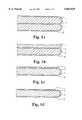
- FIGS. 1a through 1dshow steps of a process for fabricating an SOI substrate in accordance with the present invention.
- FIGS. 2a through 2fshow steps of a process for fabricating an SOI substrate in accordance with the conventional technique.
- the process for fabricating the SOI substrate of the present inventioncan be described as follows.
- a semiconductor wafer of an active substrate 1 and a semiconductor wafer of a supporting substrate 2are bonded together to form a bonded wafer 4 surrounded with oxide films 3.
- the active substrate 1is subjected to surface-grinding to reduce its thickness to 15 ⁇ m.
- the active substrate 1is then subjected to spin etching to reduce its thickness to 3 ⁇ m.
- the active substrate 1is thin film formed by PACE processing to reduce its thickness to 0.1-0.2 ⁇ m.
- the program of the PACE processingis set such as to remove the peripheral portion of the active substrate 1, therefore, at the same time as the thin film forming, the non-bonded peripheral portion of the bonded wafer 4 can be removed.
- the etching solution used in the spin etchingis preferably a mixed acid, for example, a mixed solution of hydrofluoric acid, nitric acid, n-phosphoric acid(H 3 PO 4 ) and sulfuric acid.
- the fabricating process of the present inventionsince the L-shaped grinding and alkaline etching steps in the conventional process are omitted, therefore, the fabrication time is extensively shortened. Moreover, comparing the spin etching of the present invention with the conventional polishing, the lead time is shortened, thus the fabrication efficiency is further increased.
- Table 1shows the differences in fabrication efficiency between the process of the present invention and that of the conventional process.
- the present inventionsince the non-bonded peripheral portion of the bonded wafer is removed by PACE processing, therefore, the present invention has the additional advantage of greatly reducing the scratch which is easily formed on the peripheral portion.
Landscapes
- Engineering & Computer Science (AREA)
- Physics & Mathematics (AREA)
- Condensed Matter Physics & Semiconductors (AREA)
- General Physics & Mathematics (AREA)
- Manufacturing & Machinery (AREA)
- Computer Hardware Design (AREA)
- Microelectronics & Electronic Packaging (AREA)
- Power Engineering (AREA)
- Mechanical Treatment Of Semiconductor (AREA)
- Weting (AREA)
- Thin Film Transistor (AREA)
Abstract
Description
1. Field of the Invention
The present invention relates to a process for fabricating an SOI substrate-by subjecting a bonded wafer composed of a semiconductor wafer of an active substrate bonded on by a semiconductor wafer of a supporting substrate to PACE (plasma assisted chemical etching) process to form the active substrate into a thin film.
2. Description of the Prior Art
The demand for SOI substrates has continuously increased in recent years, in order to make integrated circuits operatable at higher speeds. Particularly, SOI substrates including active substrates which are thin films have been commonly used to make integrated circuits operate at even further higher speeds. A conventional SOI substrate including an active substrate which is a thin film is fabricated by the following steps:
(1) bonding a semiconductor wafer of an active substrate 11 and a semiconductor wafer of a supporting substrate 12 to form a bonded wafer 14 (referring to FIG. 2a);
(2) L-shaped-grinding the peripheral edge of the active substrate 11 of the bonded wafer 14 (referring to FIG. 2b);
(3) alkaline etching the L-shaped-grinded bondedwafer 14 to remove the surroundingoxide film 13 and the non-attached portion of the peripheral edge (referring to FIG. 2c);
(4) surface grinding the alkaline etched. active substrate 11 of thebonded wafer 14 to reduce the thickness of the active substrate (referring to FIG. 2d);
(5) polishing the surface ground active substrate 11 to further reduce its thickness (referring to FIG. 2e); and
(6) PACE processing the polished active substrate 11 to form the active substrate into a thin film (referring to FIG. 2f).
However, the above-mentioned process suffers from the disadvantage that it is difficult to control the etching rate, and at a peripheral edge of the substrate scratches are formed easily.
In addition, the lead time required for L-grinding and alkaline etching is too long, thus the output of the fabrication quantity is limited, resulting in unsatisfactory efficiency.
An object of the present invention is to solve the above-mentioned problems and provide a process for fabricating an SOI substrate with no peripheral scratches and with enhanced fabrication efficiency.
According to the present invention, the process for fabricating the SOI substrate of the present invention comprises subjecting a bonded wafer, in which the bonded wafer consists of a semiconductor wafer of an active substrate bonded on by a semiconductor wafer of a supporting substrate, to PACE (plasma assisted chemical etching) process to form the active substrate into a thin film so as to obtain the SOI substrate, characterized in that a non-bonded peripheral portion of the bonded wafer is removed by the PACE process.
Furthermore, the process for fabricating the SOI substrate comprises bonding a semiconductor wafer of an active substrate and a semiconductor wafer of a supporting substrate to form a bonded wafer; surface-grinding the active substrate; spin etching the active substrate; and finally PACE processing the etched active substrate to form the etched active substrate into a thin film and simultaneouly to remove the non-bonded peripheral portion of the bonded wafer.
FIGS. 1a through 1d show steps of a process for fabricating an SOI substrate in accordance with the present invention.
FIGS. 2a through 2f show steps of a process for fabricating an SOI substrate in accordance with the conventional technique.
The process for fabricating the SOI substrate of the present invention will be explained by the following examples accompanied by the drawings.
The process for fabricating the SOI substrate of the present invention can be described as follows.
(1) Referring to FIG. 1a, just as with the conventional process, a semiconductor wafer of anactive substrate 1 and a semiconductor wafer of a supportingsubstrate 2 are bonded together to form abonded wafer 4 surrounded withoxide films 3.
(2) Referring to FIG. 1b, theactive substrate 1 is subjected to surface-grinding to reduce its thickness to 15 μm.
(3) Referring to FIG. 1c, theactive substrate 1 is then subjected to spin etching to reduce its thickness to 3 μm.
(4) Referring to FIG. 1d, theactive substrate 1 is thin film formed by PACE processing to reduce its thickness to 0.1-0.2 μm. At that time, the program of the PACE processing is set such as to remove the peripheral portion of theactive substrate 1, therefore, at the same time as the thin film forming, the non-bonded peripheral portion of thebonded wafer 4 can be removed.
In order to prevent uneven processing and to control the etching rate, the etching solution used in the spin etching is preferably a mixed acid, for example, a mixed solution of hydrofluoric acid, nitric acid, n-phosphoric acid(H3 PO4) and sulfuric acid.
According to the fabricating process of the present invention, since the L-shaped grinding and alkaline etching steps in the conventional process are omitted, therefore, the fabrication time is extensively shortened. Moreover, comparing the spin etching of the present invention with the conventional polishing, the lead time is shortened, thus the fabrication efficiency is further increased.
An example of the present invention is explained as follows.
Table 1 shows the differences in fabrication efficiency between the process of the present invention and that of the conventional process.
TABLE 1______________________________________The processing time for fabricating 1000 SOI substrates Fabricating process Processing time (hours)Processing Conventional Presentsteps technique invention______________________________________L-grinding 128 --Alkaline etching 70 --Plane grinding 50 50Polishing 250 --Spin etching -- 42PACE processing 84 117Total 582 209______________________________________
As can be seen clearly in Table 1, according to the conventional process, it takes about 582 hours to fabricate 1000 SOI substrates, while according to the present invention, it takes only about one third of the conventional time (i.e., 209 hours) to fabricate the same quantity of SOI substrates. Therefore, the fabrication efficiency is considerably enhanced by employing the present invention.
Since the present invention saves some of the processing steps of the conventional process, the fabrication efficiency is considerably enhanced.
Moreover, since the non-bonded peripheral portion of the bonded wafer is removed by PACE processing, therefore, the present invention has the additional advantage of greatly reducing the scratch which is easily formed on the peripheral portion.
Claims (4)
1. A process for fabricating an SOI substrate, comprising subjecting a bonded wafer, in which the bonded wafer is composed of a semiconductor wafer of an active substrate bonded on by a semiconductor base wafer, to PACE (plasma assisted chemical etching) process to form the active substrate into a thin film so as to obtain the SOI substrate, characterized in that a non-bonded peripheral portion of the bonded wafer is simultaneously removed by the PACE process.
2. A process for fabricating an SOI substrate, characterized in that the process comprises the following steps of:
(1) bonding a semiconductor wafer of an active substrate and a semiconductor base wafer to form a bonded wafer;
(2) surface-grinding the active substrate of the bonded wafer;
(3) etching the surface-ground active substrate by spin etching; and
(4) PACE processing the etched active substrate to form the etched active substrate into a thin film and simultaneously to remove a non-bonded peripheral portion of the bonded wafer.
3. The process for fabricating an SOI substrate as. claimed in claim 2, wherein an etching solution used in the spin etching is a mixed acid.
4. The process for fabricating an SOI substrate as claimed in claim 3, wherein the mixed acid comprises hydrofluoric acid, nitric acid, n-phosphoric acid and sulfuric acid.
Priority Applications (2)
| Application Number | Priority Date | Filing Date | Title |
|---|---|---|---|
| JP7254424AJPH0964321A (en) | 1995-08-24 | 1995-08-24 | Manufacture of soi substrate |
| US08/748,406US5863829A (en) | 1995-08-24 | 1996-11-13 | Process for fabricating SOI substrate |
Applications Claiming Priority (2)
| Application Number | Priority Date | Filing Date | Title |
|---|---|---|---|
| JP7254424AJPH0964321A (en) | 1995-08-24 | 1995-08-24 | Manufacture of soi substrate |
| US08/748,406US5863829A (en) | 1995-08-24 | 1996-11-13 | Process for fabricating SOI substrate |
Publications (1)
| Publication Number | Publication Date |
|---|---|
| US5863829Atrue US5863829A (en) | 1999-01-26 |
Family
ID=26541681
Family Applications (1)
| Application Number | Title | Priority Date | Filing Date |
|---|---|---|---|
| US08/748,406Expired - Fee RelatedUS5863829A (en) | 1995-08-24 | 1996-11-13 | Process for fabricating SOI substrate |
Country Status (2)
| Country | Link |
|---|---|
| US (1) | US5863829A (en) |
| JP (1) | JPH0964321A (en) |
Cited By (38)
| Publication number | Priority date | Publication date | Assignee | Title |
|---|---|---|---|---|
| US6090688A (en)* | 1996-11-15 | 2000-07-18 | Komatsu Electronic Metals Co., Ltd. | Method for fabricating an SOI substrate |
| US6096433A (en)* | 1997-02-20 | 2000-08-01 | Nec Corporation | Laminated substrate fabricated from semiconductor wafers bonded to each other without contact between insulating layer and semiconductor layer and process of fabrication thereof |
| US6110391A (en)* | 1997-01-17 | 2000-08-29 | Shin-Etsu Handotai Co., Ltd. | Method of manufacturing a bonding substrate |
| US6117778A (en)* | 1998-02-11 | 2000-09-12 | International Business Machines Corporation | Semiconductor wafer edge bead removal method and tool |
| EP0964436A3 (en)* | 1998-06-04 | 2000-10-18 | Shin-Etsu Handotai Company Limited | Method for manufacturing SOI wafer and SOI wafer |
| WO2000072366A1 (en)* | 1999-05-21 | 2000-11-30 | Plasmasil, L.L.C. | Method for improving thickness uniformity of semiconductor wafers |
| WO2001027999A1 (en)* | 1999-10-14 | 2001-04-19 | Shin-Etsu Handotai Co., Ltd. | Bonded wafer producing method and bonded wafer |
| US6294469B1 (en) | 1999-05-21 | 2001-09-25 | Plasmasil, Llc | Silicon wafering process flow |
| US6391743B1 (en) | 1998-09-22 | 2002-05-21 | Canon Kabushiki Kaisha | Method and apparatus for producing photoelectric conversion device |
| KR100338220B1 (en)* | 1999-09-02 | 2002-05-24 | 이 창 세 | Fabrication method of substrate for silicon on glass wafer |
| US20020100751A1 (en)* | 2001-01-30 | 2002-08-01 | Carr Jeffrey W. | Apparatus and method for atmospheric pressure reactive atom plasma processing for surface modification |
| US20020155661A1 (en)* | 1999-10-28 | 2002-10-24 | Massingill Thomas J. | Multi-chip module and method for forming and method for deplating defective capacitors |
| US6521515B1 (en) | 2000-09-15 | 2003-02-18 | Advanced Micro Devices, Inc. | Deeply doped source/drains for reduction of silicide/silicon interface roughness |
| DE10220647C1 (en)* | 2002-05-08 | 2003-08-21 | Infineon Technologies Ag | Semiconductor wafer peripheral edge shaping method has material removed from peripheral edge of wafer until surface layer applied to inner part of one of its major surfaces is reached |
| US6624047B1 (en)* | 1999-02-02 | 2003-09-23 | Canon Kabushiki Kaisha | Substrate and method of manufacturing the same |
| US6660177B2 (en) | 2001-11-07 | 2003-12-09 | Rapt Industries Inc. | Apparatus and method for reactive atom plasma processing for material deposition |
| US20060128078A1 (en)* | 2004-12-15 | 2006-06-15 | Ryuji Moriwaki | SOI substrate manufacturing method |
| US20070224821A1 (en)* | 2004-09-06 | 2007-09-27 | Sumco Corporation | Method for Manufacturing Silicon Wafers |
| US20080011332A1 (en)* | 2002-04-26 | 2008-01-17 | Accretech Usa, Inc. | Method and apparatus for cleaning a wafer substrate |
| US20080017316A1 (en)* | 2002-04-26 | 2008-01-24 | Accretech Usa, Inc. | Clean ignition system for wafer substrate processing |
| US20080029485A1 (en)* | 2003-08-14 | 2008-02-07 | Rapt Industries, Inc. | Systems and Methods for Precision Plasma Processing |
| US20080035612A1 (en)* | 2003-08-14 | 2008-02-14 | Rapt Industries, Inc. | Systems and Methods Utilizing an Aperture with a Reactive Atom Plasma Torch |
| US20080063840A1 (en)* | 2004-05-28 | 2008-03-13 | Etsurou Morita | Silicon-on Insulator Substrate and Method for manufacturing the Same |
| US7371992B2 (en) | 2003-03-07 | 2008-05-13 | Rapt Industries, Inc. | Method for non-contact cleaning of a surface |
| US20080190558A1 (en)* | 2002-04-26 | 2008-08-14 | Accretech Usa, Inc. | Wafer processing apparatus and method |
| US20080217310A1 (en)* | 2007-03-09 | 2008-09-11 | Harald Fischer | Method for profiling the perimeter border of a semiconductor wafer |
| US20080315349A1 (en)* | 2005-02-28 | 2008-12-25 | Shin-Etsu Handotai Co., Ltd. | Method for Manufacturing Bonded Wafer and Bonded Wafer |
| US7510664B2 (en) | 2001-01-30 | 2009-03-31 | Rapt Industries, Inc. | Apparatus and method for atmospheric pressure reactive atom plasma processing for shaping of damage free surfaces |
| US20090095399A1 (en)* | 2004-12-28 | 2009-04-16 | Commissariat A L'energie Atomique | Method for trimming a structure obtained by the assembly of two plates |
| US20090170285A1 (en)* | 2006-05-29 | 2009-07-02 | Shin-Etsu Handotai Co., Ltd. | Method for manufacturing bonded wafer |
| US20120058623A1 (en)* | 2010-09-02 | 2012-03-08 | Cheng-Yu Hsieh | Method for Thinning Wafer |
| US20120129318A1 (en)* | 2010-11-24 | 2012-05-24 | Semiconductor Energy Laboratory Co., Ltd. | Atmospheric pressure plasma etching apparatus and method for manufacturing soi substrate |
| US20130237032A1 (en)* | 2012-03-06 | 2013-09-12 | Memc Electronic Materials, Inc. | Method of Manufacturing Silicon-On-Insulator Wafers |
| US20140264368A1 (en)* | 2013-03-15 | 2014-09-18 | Semiconductor Components Industries, Llc | Semiconductor Wafer and a Process of Forming the Same |
| CN108022938A (en)* | 2016-10-31 | 2018-05-11 | 中芯国际集成电路制造(上海)有限公司 | A kind of manufacture method of semiconductor devices |
| US10347525B2 (en) | 2015-10-28 | 2019-07-09 | Shin-Etsu Handotai Co., Ltd. | Method for producing bonded SOI wafer |
| US10651032B2 (en)* | 2016-08-11 | 2020-05-12 | Commissariat A L'energie Atomique Et Aux Energies Alternatives | Method for producing an epitaxial layer on a growth plate |
| US20220223475A1 (en)* | 2019-05-23 | 2022-07-14 | Tokyo Electron Limited | Substrate processing method and substrate processing system |
Families Citing this family (6)
| Publication number | Priority date | Publication date | Assignee | Title |
|---|---|---|---|---|
| JP4304879B2 (en) | 2001-04-06 | 2009-07-29 | 信越半導体株式会社 | Method for determining the implantation amount of hydrogen ions or rare gas ions |
| JP3944087B2 (en) | 2003-01-21 | 2007-07-11 | 株式会社東芝 | Method for manufacturing element forming substrate |
| JP2004235478A (en)* | 2003-01-30 | 2004-08-19 | Sumitomo Mitsubishi Silicon Corp | Stacked soi substrate and its manufacturing method |
| KR100898649B1 (en)* | 2004-05-28 | 2009-05-22 | 가부시키가이샤 섬코 | SOI substrate and its manufacturing method |
| JP4892201B2 (en)* | 2005-05-13 | 2012-03-07 | ダイトエレクトロン株式会社 | Method and apparatus for processing step of outer peripheral edge of bonded workpiece |
| JP5411438B2 (en)* | 2008-03-18 | 2014-02-12 | 信越化学工業株式会社 | Manufacturing method of SOI substrate |
Citations (7)
| Publication number | Priority date | Publication date | Assignee | Title |
|---|---|---|---|---|
| US5032544A (en)* | 1989-08-17 | 1991-07-16 | Shin-Etsu Handotai Co., Ltd. | Process for producing semiconductor device substrate using polishing guard |
| US5233218A (en)* | 1990-09-20 | 1993-08-03 | Fujitsu Limited | Semiconductor wafer and process for producing same |
| US5258323A (en)* | 1992-12-29 | 1993-11-02 | Honeywell Inc. | Single crystal silicon on quartz |
| JPH07211876A (en)* | 1994-01-21 | 1995-08-11 | Canon Inc | Method for making semiconductor substrate |
| US5494849A (en)* | 1995-03-23 | 1996-02-27 | Si Bond L.L.C. | Single-etch stop process for the manufacture of silicon-on-insulator substrates |
| JPH08274286A (en)* | 1995-03-29 | 1996-10-18 | Komatsu Electron Metals Co Ltd | Manufacture of soi substrate |
| US5668045A (en)* | 1994-11-30 | 1997-09-16 | Sibond, L.L.C. | Process for stripping outer edge of BESOI wafers |
- 1995
- 1995-08-24JPJP7254424Apatent/JPH0964321A/enactivePending
- 1996
- 1996-11-13USUS08/748,406patent/US5863829A/ennot_activeExpired - Fee Related
Patent Citations (7)
| Publication number | Priority date | Publication date | Assignee | Title |
|---|---|---|---|---|
| US5032544A (en)* | 1989-08-17 | 1991-07-16 | Shin-Etsu Handotai Co., Ltd. | Process for producing semiconductor device substrate using polishing guard |
| US5233218A (en)* | 1990-09-20 | 1993-08-03 | Fujitsu Limited | Semiconductor wafer and process for producing same |
| US5258323A (en)* | 1992-12-29 | 1993-11-02 | Honeywell Inc. | Single crystal silicon on quartz |
| JPH07211876A (en)* | 1994-01-21 | 1995-08-11 | Canon Inc | Method for making semiconductor substrate |
| US5668045A (en)* | 1994-11-30 | 1997-09-16 | Sibond, L.L.C. | Process for stripping outer edge of BESOI wafers |
| US5494849A (en)* | 1995-03-23 | 1996-02-27 | Si Bond L.L.C. | Single-etch stop process for the manufacture of silicon-on-insulator substrates |
| JPH08274286A (en)* | 1995-03-29 | 1996-10-18 | Komatsu Electron Metals Co Ltd | Manufacture of soi substrate |
Cited By (60)
| Publication number | Priority date | Publication date | Assignee | Title |
|---|---|---|---|---|
| US6090688A (en)* | 1996-11-15 | 2000-07-18 | Komatsu Electronic Metals Co., Ltd. | Method for fabricating an SOI substrate |
| US6110391A (en)* | 1997-01-17 | 2000-08-29 | Shin-Etsu Handotai Co., Ltd. | Method of manufacturing a bonding substrate |
| US6346435B1 (en) | 1997-02-20 | 2002-02-12 | Nec Corporation | Laminated substrate fabricated from semiconductor wafers bonded to each other without contact between insulating layer and semiconductor layer and process of fabrication thereof |
| US6096433A (en)* | 1997-02-20 | 2000-08-01 | Nec Corporation | Laminated substrate fabricated from semiconductor wafers bonded to each other without contact between insulating layer and semiconductor layer and process of fabrication thereof |
| US6117778A (en)* | 1998-02-11 | 2000-09-12 | International Business Machines Corporation | Semiconductor wafer edge bead removal method and tool |
| US6497784B1 (en) | 1998-02-11 | 2002-12-24 | International Business Machines Corporation | Semiconductor wafer edge bead removal method and tool |
| EP0964436A3 (en)* | 1998-06-04 | 2000-10-18 | Shin-Etsu Handotai Company Limited | Method for manufacturing SOI wafer and SOI wafer |
| US6534384B2 (en)* | 1998-06-04 | 2003-03-18 | Shin-Etsu Handotai Co., Ltd. | Method for manufacturing SOI wafer including heat treatment in an oxidizing atmosphere |
| US6391743B1 (en) | 1998-09-22 | 2002-05-21 | Canon Kabushiki Kaisha | Method and apparatus for producing photoelectric conversion device |
| US6624047B1 (en)* | 1999-02-02 | 2003-09-23 | Canon Kabushiki Kaisha | Substrate and method of manufacturing the same |
| US6294469B1 (en) | 1999-05-21 | 2001-09-25 | Plasmasil, Llc | Silicon wafering process flow |
| WO2000072366A1 (en)* | 1999-05-21 | 2000-11-30 | Plasmasil, L.L.C. | Method for improving thickness uniformity of semiconductor wafers |
| KR100338220B1 (en)* | 1999-09-02 | 2002-05-24 | 이 창 세 | Fabrication method of substrate for silicon on glass wafer |
| WO2001027999A1 (en)* | 1999-10-14 | 2001-04-19 | Shin-Etsu Handotai Co., Ltd. | Bonded wafer producing method and bonded wafer |
| KR100733112B1 (en)* | 1999-10-14 | 2007-06-27 | 신에쯔 한도타이 가부시키가이샤 | Manufacturing method of bonded wafer |
| US20020155661A1 (en)* | 1999-10-28 | 2002-10-24 | Massingill Thomas J. | Multi-chip module and method for forming and method for deplating defective capacitors |
| US6882045B2 (en) | 1999-10-28 | 2005-04-19 | Thomas J. Massingill | Multi-chip module and method for forming and method for deplating defective capacitors |
| US6521515B1 (en) | 2000-09-15 | 2003-02-18 | Advanced Micro Devices, Inc. | Deeply doped source/drains for reduction of silicide/silicon interface roughness |
| US7591957B2 (en) | 2001-01-30 | 2009-09-22 | Rapt Industries, Inc. | Method for atmospheric pressure reactive atom plasma processing for surface modification |
| US7510664B2 (en) | 2001-01-30 | 2009-03-31 | Rapt Industries, Inc. | Apparatus and method for atmospheric pressure reactive atom plasma processing for shaping of damage free surfaces |
| US20050000656A1 (en)* | 2001-01-30 | 2005-01-06 | Rapt Industries, Inc. | Apparatus for atmospheric pressure reactive atom plasma processing for surface modification |
| US20020100751A1 (en)* | 2001-01-30 | 2002-08-01 | Carr Jeffrey W. | Apparatus and method for atmospheric pressure reactive atom plasma processing for surface modification |
| US7955513B2 (en) | 2001-11-07 | 2011-06-07 | Rapt Industries, Inc. | Apparatus and method for reactive atom plasma processing for material deposition |
| US7311851B2 (en) | 2001-11-07 | 2007-12-25 | Rapt Industries, Inc. | Apparatus and method for reactive atom plasma processing for material deposition |
| US20040200802A1 (en)* | 2001-11-07 | 2004-10-14 | Rapt. Industries Inc. | Apparatus and method for reactive atom plasma processing for material deposition |
| US6660177B2 (en) | 2001-11-07 | 2003-12-09 | Rapt Industries Inc. | Apparatus and method for reactive atom plasma processing for material deposition |
| US20080099441A1 (en)* | 2001-11-07 | 2008-05-01 | Rapt Industries, Inc. | Apparatus and method for reactive atom plasma processing for material deposition |
| US20080011332A1 (en)* | 2002-04-26 | 2008-01-17 | Accretech Usa, Inc. | Method and apparatus for cleaning a wafer substrate |
| US20080017316A1 (en)* | 2002-04-26 | 2008-01-24 | Accretech Usa, Inc. | Clean ignition system for wafer substrate processing |
| US20080190558A1 (en)* | 2002-04-26 | 2008-08-14 | Accretech Usa, Inc. | Wafer processing apparatus and method |
| DE10220647C1 (en)* | 2002-05-08 | 2003-08-21 | Infineon Technologies Ag | Semiconductor wafer peripheral edge shaping method has material removed from peripheral edge of wafer until surface layer applied to inner part of one of its major surfaces is reached |
| US7371992B2 (en) | 2003-03-07 | 2008-05-13 | Rapt Industries, Inc. | Method for non-contact cleaning of a surface |
| US20080035612A1 (en)* | 2003-08-14 | 2008-02-14 | Rapt Industries, Inc. | Systems and Methods Utilizing an Aperture with a Reactive Atom Plasma Torch |
| US20080029485A1 (en)* | 2003-08-14 | 2008-02-07 | Rapt Industries, Inc. | Systems and Methods for Precision Plasma Processing |
| US20080063840A1 (en)* | 2004-05-28 | 2008-03-13 | Etsurou Morita | Silicon-on Insulator Substrate and Method for manufacturing the Same |
| EP1758168B1 (en)* | 2004-05-28 | 2020-02-19 | Sumco Corporation | Soi substrate and method for producing same |
| US7736998B2 (en) | 2004-05-28 | 2010-06-15 | Sumco Corporation | Silicon-on insulator substrate and method for manufacturing the same |
| US20070224821A1 (en)* | 2004-09-06 | 2007-09-27 | Sumco Corporation | Method for Manufacturing Silicon Wafers |
| US7601644B2 (en)* | 2004-09-06 | 2009-10-13 | Sumco Corporation | Method for manufacturing silicon wafers |
| US20060128078A1 (en)* | 2004-12-15 | 2006-06-15 | Ryuji Moriwaki | SOI substrate manufacturing method |
| US7368332B2 (en)* | 2004-12-15 | 2008-05-06 | Canon Kabushiki Kaisha | SOI substrate manufacturing method |
| US8628674B2 (en) | 2004-12-28 | 2014-01-14 | Commissariat A L'energie Atomique Et Aux Energies Alternatives | Method for trimming a structure obtained by the assembly of two plates |
| US8329048B2 (en)* | 2004-12-28 | 2012-12-11 | Commissariat A L'energie Atomique | Method for trimming a structure obtained by the assembly of two plates |
| US20090095399A1 (en)* | 2004-12-28 | 2009-04-16 | Commissariat A L'energie Atomique | Method for trimming a structure obtained by the assembly of two plates |
| US20080315349A1 (en)* | 2005-02-28 | 2008-12-25 | Shin-Etsu Handotai Co., Ltd. | Method for Manufacturing Bonded Wafer and Bonded Wafer |
| US7776719B2 (en) | 2006-05-29 | 2010-08-17 | Shin-Etsu Handotai Co., Ltd. | Method for manufacturing bonded wafer |
| US20090170285A1 (en)* | 2006-05-29 | 2009-07-02 | Shin-Etsu Handotai Co., Ltd. | Method for manufacturing bonded wafer |
| US20080217310A1 (en)* | 2007-03-09 | 2008-09-11 | Harald Fischer | Method for profiling the perimeter border of a semiconductor wafer |
| US20120058623A1 (en)* | 2010-09-02 | 2012-03-08 | Cheng-Yu Hsieh | Method for Thinning Wafer |
| US8278189B2 (en)* | 2010-09-02 | 2012-10-02 | United Microelectronics Corp. | Method for thinning wafer |
| US20120129318A1 (en)* | 2010-11-24 | 2012-05-24 | Semiconductor Energy Laboratory Co., Ltd. | Atmospheric pressure plasma etching apparatus and method for manufacturing soi substrate |
| US20130237032A1 (en)* | 2012-03-06 | 2013-09-12 | Memc Electronic Materials, Inc. | Method of Manufacturing Silicon-On-Insulator Wafers |
| US8853054B2 (en)* | 2012-03-06 | 2014-10-07 | Sunedison Semiconductor Limited | Method of manufacturing silicon-on-insulator wafers |
| US20140264368A1 (en)* | 2013-03-15 | 2014-09-18 | Semiconductor Components Industries, Llc | Semiconductor Wafer and a Process of Forming the Same |
| US9245736B2 (en)* | 2013-03-15 | 2016-01-26 | Semiconductor Components Industries, Llc | Process of forming a semiconductor wafer |
| US9842899B2 (en) | 2013-03-15 | 2017-12-12 | Semiconductor Components Industries, Llc | Semiconductor wafer including a monocrystalline semiconductor layer spaced apart from a poly template layer |
| US10347525B2 (en) | 2015-10-28 | 2019-07-09 | Shin-Etsu Handotai Co., Ltd. | Method for producing bonded SOI wafer |
| US10651032B2 (en)* | 2016-08-11 | 2020-05-12 | Commissariat A L'energie Atomique Et Aux Energies Alternatives | Method for producing an epitaxial layer on a growth plate |
| CN108022938A (en)* | 2016-10-31 | 2018-05-11 | 中芯国际集成电路制造(上海)有限公司 | A kind of manufacture method of semiconductor devices |
| US20220223475A1 (en)* | 2019-05-23 | 2022-07-14 | Tokyo Electron Limited | Substrate processing method and substrate processing system |
Also Published As
| Publication number | Publication date |
|---|---|
| JPH0964321A (en) | 1997-03-07 |
Similar Documents
| Publication | Publication Date | Title |
|---|---|---|
| US5863829A (en) | Process for fabricating SOI substrate | |
| US5344524A (en) | SOI substrate fabrication | |
| US5659192A (en) | SOI substrate fabrication | |
| US5918139A (en) | Method of manufacturing a bonding substrate | |
| US6090688A (en) | Method for fabricating an SOI substrate | |
| JPH11219873A (en) | Improvement of mechanical resistance of single crystal silicon wafer | |
| JPH04298037A (en) | Manufacture of integrated silicon/non-silicon semiconductor device | |
| US5081061A (en) | Manufacturing ultra-thin dielectrically isolated wafers | |
| JPH0799295A (en) | Method of making semiconductor substrate and semiconductor substrate | |
| JP3632531B2 (en) | Manufacturing method of semiconductor substrate | |
| US5849636A (en) | Method for fabricating a semiconductor wafer | |
| KR20040060990A (en) | Method for producing cemented wafer | |
| KR970012965A (en) | SOI wafer and manufacturing method thereof | |
| KR19980069868A (en) | Multi-thickness silicon wafers on insulators that highly integrate mixed signal integrated circuit devices | |
| KR940010159B1 (en) | Manufacturing Method of Semiconductor Substrate | |
| JP3524009B2 (en) | SOI wafer and method for manufacturing the same | |
| JP2003151939A (en) | Method of manufacturing soi substrate | |
| JP2766417B2 (en) | Manufacturing method of bonded dielectric separation wafer | |
| JPH08274286A (en) | Manufacture of soi substrate | |
| JP3160966B2 (en) | Method for manufacturing SOI substrate | |
| JPH03270254A (en) | Manufacturing method of semiconductor device | |
| KR100327326B1 (en) | Manufacturing method of S.O.wafer | |
| JPH02237066A (en) | Manufacture of semiconductor device | |
| JPH03268444A (en) | Manufacturing method of semiconductor device | |
| JP2728310B2 (en) | Semiconductor wafer gettering method |
Legal Events
| Date | Code | Title | Description |
|---|---|---|---|
| AS | Assignment | Owner name:KOMATSU ELECTRONIC METALS CO., LTD., JAPAN Free format text:ASSIGNMENT OF ASSIGNORS INTEREST;ASSIGNORS:NAKAYOSHI, YUICHI;YAMAMOTO, HIROAKI;ISHII, AKIHIRO;REEL/FRAME:008314/0194 Effective date:19961105 | |
| FEPP | Fee payment procedure | Free format text:PAYOR NUMBER ASSIGNED (ORIGINAL EVENT CODE: ASPN); ENTITY STATUS OF PATENT OWNER: LARGE ENTITY | |
| REMI | Maintenance fee reminder mailed | ||
| LAPS | Lapse for failure to pay maintenance fees | ||
| STCH | Information on status: patent discontinuation | Free format text:PATENT EXPIRED DUE TO NONPAYMENT OF MAINTENANCE FEES UNDER 37 CFR 1.362 | |
| FP | Lapsed due to failure to pay maintenance fee | Effective date:20030126 |