US5861651A - Field effect devices and capacitors with improved thin film dielectrics and method for making same - Google Patents
Field effect devices and capacitors with improved thin film dielectrics and method for making sameDownload PDFInfo
- Publication number
- US5861651A US5861651AUS08/807,209US80720997AUS5861651AUS 5861651 AUS5861651 AUS 5861651AUS 80720997 AUS80720997 AUS 80720997AUS 5861651 AUS5861651 AUS 5861651A
- Authority
- US
- United States
- Prior art keywords
- angstroms
- nitrogen
- channel
- maximum
- doped
- Prior art date
- Legal status (The legal status is an assumption and is not a legal conclusion. Google has not performed a legal analysis and makes no representation as to the accuracy of the status listed.)
- Expired - Lifetime
Links
Images

Classifications
- H—ELECTRICITY
- H01—ELECTRIC ELEMENTS
- H01L—SEMICONDUCTOR DEVICES NOT COVERED BY CLASS H10
- H01L21/00—Processes or apparatus adapted for the manufacture or treatment of semiconductor or solid state devices or of parts thereof
- H01L21/02—Manufacture or treatment of semiconductor devices or of parts thereof
- H01L21/04—Manufacture or treatment of semiconductor devices or of parts thereof the devices having potential barriers, e.g. a PN junction, depletion layer or carrier concentration layer
- H01L21/18—Manufacture or treatment of semiconductor devices or of parts thereof the devices having potential barriers, e.g. a PN junction, depletion layer or carrier concentration layer the devices having semiconductor bodies comprising elements of Group IV of the Periodic Table or AIIIBV compounds with or without impurities, e.g. doping materials
- H01L21/28—Manufacture of electrodes on semiconductor bodies using processes or apparatus not provided for in groups H01L21/20 - H01L21/268
- H01L21/28008—Making conductor-insulator-semiconductor electrodes
- H01L21/28017—Making conductor-insulator-semiconductor electrodes the insulator being formed after the semiconductor body, the semiconductor being silicon
- H01L21/28158—Making the insulator
- H01L21/28167—Making the insulator on single crystalline silicon, e.g. using a liquid, i.e. chemical oxidation
- H01L21/28185—Making the insulator on single crystalline silicon, e.g. using a liquid, i.e. chemical oxidation with a treatment, e.g. annealing, after the formation of the gate insulator and before the formation of the definitive gate conductor
- H—ELECTRICITY
- H01—ELECTRIC ELEMENTS
- H01L—SEMICONDUCTOR DEVICES NOT COVERED BY CLASS H10
- H01L21/00—Processes or apparatus adapted for the manufacture or treatment of semiconductor or solid state devices or of parts thereof
- H01L21/02—Manufacture or treatment of semiconductor devices or of parts thereof
- H01L21/02104—Forming layers
- H01L21/02107—Forming insulating materials on a substrate
- H01L21/02109—Forming insulating materials on a substrate characterised by the type of layer, e.g. type of material, porous/non-porous, pre-cursors, mixtures or laminates
- H01L21/02112—Forming insulating materials on a substrate characterised by the type of layer, e.g. type of material, porous/non-porous, pre-cursors, mixtures or laminates characterised by the material of the layer
- H01L21/02123—Forming insulating materials on a substrate characterised by the type of layer, e.g. type of material, porous/non-porous, pre-cursors, mixtures or laminates characterised by the material of the layer the material containing silicon
- H01L21/02126—Forming insulating materials on a substrate characterised by the type of layer, e.g. type of material, porous/non-porous, pre-cursors, mixtures or laminates characterised by the material of the layer the material containing silicon the material containing Si, O, and at least one of H, N, C, F, or other non-metal elements, e.g. SiOC, SiOC:H or SiONC
- H01L21/0214—Forming insulating materials on a substrate characterised by the type of layer, e.g. type of material, porous/non-porous, pre-cursors, mixtures or laminates characterised by the material of the layer the material containing silicon the material containing Si, O, and at least one of H, N, C, F, or other non-metal elements, e.g. SiOC, SiOC:H or SiONC the material being a silicon oxynitride, e.g. SiON or SiON:H
- H—ELECTRICITY
- H01—ELECTRIC ELEMENTS
- H01L—SEMICONDUCTOR DEVICES NOT COVERED BY CLASS H10
- H01L21/00—Processes or apparatus adapted for the manufacture or treatment of semiconductor or solid state devices or of parts thereof
- H01L21/02—Manufacture or treatment of semiconductor devices or of parts thereof
- H01L21/02104—Forming layers
- H01L21/02107—Forming insulating materials on a substrate
- H01L21/02225—Forming insulating materials on a substrate characterised by the process for the formation of the insulating layer
- H01L21/02227—Forming insulating materials on a substrate characterised by the process for the formation of the insulating layer formation by a process other than a deposition process
- H01L21/02249—Forming insulating materials on a substrate characterised by the process for the formation of the insulating layer formation by a process other than a deposition process formation by combined oxidation and nitridation performed simultaneously
- H—ELECTRICITY
- H01—ELECTRIC ELEMENTS
- H01L—SEMICONDUCTOR DEVICES NOT COVERED BY CLASS H10
- H01L21/00—Processes or apparatus adapted for the manufacture or treatment of semiconductor or solid state devices or of parts thereof
- H01L21/02—Manufacture or treatment of semiconductor devices or of parts thereof
- H01L21/02104—Forming layers
- H01L21/02107—Forming insulating materials on a substrate
- H01L21/02225—Forming insulating materials on a substrate characterised by the process for the formation of the insulating layer
- H01L21/02227—Forming insulating materials on a substrate characterised by the process for the formation of the insulating layer formation by a process other than a deposition process
- H01L21/02255—Forming insulating materials on a substrate characterised by the process for the formation of the insulating layer formation by a process other than a deposition process formation by thermal treatment
- H—ELECTRICITY
- H01—ELECTRIC ELEMENTS
- H01L—SEMICONDUCTOR DEVICES NOT COVERED BY CLASS H10
- H01L21/00—Processes or apparatus adapted for the manufacture or treatment of semiconductor or solid state devices or of parts thereof
- H01L21/02—Manufacture or treatment of semiconductor devices or of parts thereof
- H01L21/02104—Forming layers
- H01L21/02107—Forming insulating materials on a substrate
- H01L21/02296—Forming insulating materials on a substrate characterised by the treatment performed before or after the formation of the layer
- H01L21/02318—Forming insulating materials on a substrate characterised by the treatment performed before or after the formation of the layer post-treatment
- H01L21/02337—Forming insulating materials on a substrate characterised by the treatment performed before or after the formation of the layer post-treatment treatment by exposure to a gas or vapour
- H—ELECTRICITY
- H01—ELECTRIC ELEMENTS
- H01L—SEMICONDUCTOR DEVICES NOT COVERED BY CLASS H10
- H01L21/00—Processes or apparatus adapted for the manufacture or treatment of semiconductor or solid state devices or of parts thereof
- H01L21/02—Manufacture or treatment of semiconductor devices or of parts thereof
- H01L21/04—Manufacture or treatment of semiconductor devices or of parts thereof the devices having potential barriers, e.g. a PN junction, depletion layer or carrier concentration layer
- H01L21/18—Manufacture or treatment of semiconductor devices or of parts thereof the devices having potential barriers, e.g. a PN junction, depletion layer or carrier concentration layer the devices having semiconductor bodies comprising elements of Group IV of the Periodic Table or AIIIBV compounds with or without impurities, e.g. doping materials
- H01L21/28—Manufacture of electrodes on semiconductor bodies using processes or apparatus not provided for in groups H01L21/20 - H01L21/268
- H01L21/28008—Making conductor-insulator-semiconductor electrodes
- H01L21/28017—Making conductor-insulator-semiconductor electrodes the insulator being formed after the semiconductor body, the semiconductor being silicon
- H01L21/28158—Making the insulator
- H01L21/28167—Making the insulator on single crystalline silicon, e.g. using a liquid, i.e. chemical oxidation
- H01L21/28202—Making the insulator on single crystalline silicon, e.g. using a liquid, i.e. chemical oxidation in a nitrogen-containing ambient, e.g. nitride deposition, growth, oxynitridation, NH3 nitridation, N2O oxidation, thermal nitridation, RTN, plasma nitridation, RPN
- H—ELECTRICITY
- H10—SEMICONDUCTOR DEVICES; ELECTRIC SOLID-STATE DEVICES NOT OTHERWISE PROVIDED FOR
- H10D—INORGANIC ELECTRIC SEMICONDUCTOR DEVICES
- H10D1/00—Resistors, capacitors or inductors
- H10D1/60—Capacitors
- H10D1/68—Capacitors having no potential barriers
- H—ELECTRICITY
- H10—SEMICONDUCTOR DEVICES; ELECTRIC SOLID-STATE DEVICES NOT OTHERWISE PROVIDED FOR
- H10D—INORGANIC ELECTRIC SEMICONDUCTOR DEVICES
- H10D64/00—Electrodes of devices having potential barriers
- H10D64/60—Electrodes characterised by their materials
- H10D64/66—Electrodes having a conductor capacitively coupled to a semiconductor by an insulator, e.g. MIS electrodes
- H10D64/661—Electrodes having a conductor capacitively coupled to a semiconductor by an insulator, e.g. MIS electrodes the conductor comprising a layer of silicon contacting the insulator, e.g. polysilicon having vertical doping variation
- H—ELECTRICITY
- H10—SEMICONDUCTOR DEVICES; ELECTRIC SOLID-STATE DEVICES NOT OTHERWISE PROVIDED FOR
- H10D—INORGANIC ELECTRIC SEMICONDUCTOR DEVICES
- H10D64/00—Electrodes of devices having potential barriers
- H10D64/60—Electrodes characterised by their materials
- H10D64/66—Electrodes having a conductor capacitively coupled to a semiconductor by an insulator, e.g. MIS electrodes
- H10D64/68—Electrodes having a conductor capacitively coupled to a semiconductor by an insulator, e.g. MIS electrodes characterised by the insulator, e.g. by the gate insulator
- H10D64/693—Electrodes having a conductor capacitively coupled to a semiconductor by an insulator, e.g. MIS electrodes characterised by the insulator, e.g. by the gate insulator the insulator comprising nitrogen, e.g. nitrides, oxynitrides or nitrogen-doped materials
Definitions
- This inventionrelates to electronic devices such as field effect devices and capacitors employing improved thin film dielectrics and to methods for making such devices.
- Field effect devicessuch as field effect transistors
- field effect transistorsare fundamental components in modern electronics. They are basic components in most digital and many analog circuits, including circuits for data processing and telecommunications. Indeed it has been surmised that field effect transistors are among the most numerous of human-made objects.
- Field effect devicestypically comprise a controllable-conductivity path, called a channel, disposed between a source and a drain.
- a gate electrodeis formed on a thin dielectric film overlying the channel.
- the source and the draincan be n-type regions of silicon and the channel can be a p-type region connecting them.
- the gate electrodecan be a conductively-doped polysilicon layer formed on a thin layer of silicon oxide overlying the channel.
- Capacitorsare also important components of integrated circuits.
- a typical capacitorcomprises first and second conductive layers separated by a thin dielectric film.
- capacitors and field effect deviceswork in conjunction and are formed from common layers.
- Nitrogen dopinghas been used to enhance the reliability of silicon oxide dielectrics.
- films so thin as those desired for use in VLSI and ULSI integrated circuitsit has been difficult to control the distribution of nitrogen in the film.
- an electronic deviceis provided with a thin film dielectric layer of enhanced reliability.
- the dielectriccomprises a thin film of silicon oxide having maximum concentrations of nitrogen near its major interfaces.
- the maximum adjacent the gate/SiO 2 interfaceenhances diffusion resistance to dopants from the gate.
- the maximum near the Si/SiO 2 interfaceenhances resistance to current stress.
- the concentration of nitrogenis preferably displaced slightly inward (into the oxide) from the Si/SiO 2 interface.
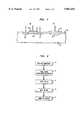
- FIG. 1is a schematic cross section of an exemplary electronic device illustrating a field effect device and a capacitor having improved dielectrics.
- FIG. 2is a flow diagram showing the steps of the preferred method of making an electronic device having an improved dielectric layer
- FIGS. 3, 4 and 5are graphical illustrations showing the nitrogen concentration profiles in a dielectric film at various stages of the process of FIG. 2.
- the field effect device 10(here a transistor) essentially comprises a source 13, a drain 14 and a channel 15, each of which can comprise a doped region of silicon supported by substrate 12.
- a gate electrode 16overlies the channel 15 and is separated from the channel by a thin dielectric film 17.
- the dielectric filmhas a pair of major interfaces adjacent the gate electrode 16 (the gate/ SiO 2 interface) and the channel 15 (the Si/SiO 2 interface).
- the filmtypically has a thickness of less than about 80 angstroms.
- the gate electrode 16is typically a thin layer of polycrystalline silicon doped to exhibit conductivity. Boron is a common dopant for this purpose, and the dielectric 17 desirably should prevent the boron from entering the dielectric.
- the dielectric 17When the field effect device is in the ON condition, current flows through the channel between the source and the drain. For reliability, the dielectric 17 must resist deterioration from collisions with electrons in this current flow.
- Capacitor 11comprises a pair of conductive layers 20 and 21 separated by a thin dielectric film 22.
- Layer 20can be conductively doped crystalline silicon and layer 21 can be a conductively-doped polycrystalline silicon film.
- the dielectric film 22should resist diffusion of impurities from the layer 20 to the layer 21.
- the dielectric filmis nitrogen-doped silicon oxide which advantageously has the same nitrogen concentration profile as described for device 10. Indeed, dielectrics 17 and 22 can be made of the same layer.
- FIG. 2illustrates the steps in making an electronic device having an improved thin film dielectric.
- the first stepis to provide a substrate having an exposed silicon surface.
- the substrateis a conventional single crystalline silicon wafer.
- the silicon surfacecan be cleaned by a conventional process used to clean silicon substrates prior to oxidation.
- the next step shown in block Bis to form a thin nitrogen-containing layer on the exposed silicon surface.
- This layerwhich is preferably nitrogen-doped silicon oxide (oxynitride), can be formed in any one of a variety of ways including heating in NO or NO 2 , chemical vapor deposition, plasma nitridation and plasma implantation. It is preferably formed by heating the substrate in a gas containing NO to produce a thin, self-limiting layer of oxynitride about 20 angstroms thick. Typical times and temperatures are 5 minutes--5 hours and 700°-1000° C., respectively. Total gas pressure can be 10 Torr or higher and is preferably 1 atm.
- This layershould contain an N concentration in the range 2 ⁇ 10 15 to 2 ⁇ 10 13 N/cm 2 . It typically contains about 7 ⁇ 10 14 N/cm 2 distributed approximately uniformly in the grown layer.
- FIG. 3An exemplary nitrogen concentration profile after this step is shown in FIG. 3.
- the bulk of the nitrogen concentrationis within 15 angstroms of the Si/SiO 2 interface.
- FIG. 4An exemplary nitrogen concentration profile after this step is shown in FIG. 4. As can be seen, the oxide growth is from the Si/SiO 2 interface, moving the N concentration into the SiO 2 region.
- the next step shown in block Dis to heat (anneal) the workpiece in a gas containing NO. This step results in little oxidation at the Si/SiO 2 interface, but further nitridation of the SiO 2 in the region adjacent the Si/SiO 2 interface. Process parameters are those described for step B.
- the final structureis typically about 50 angstroms thick, with N concentrated most heavily near the major interfaces.
- the nitrogen concentrationhas a first maximum near the gate/ SiO 2 interface (within ten angstroms) and a second (lower) maximum near the Si/SiO 2 interface.
- the N concentration in the central region between the two interfaceswould advantageously drop below both maxima.
- This structureprovides a dielectric layer with an N concentration profile closely approximating the ideal for a gate dielectric.
- the waferis again exposed to the N 2 /NO mixture for 45 minutes at 850° C., again in-situ.
- the original nitrogen in the filmis preserved.
- a fourth and optional step, in which the structure is exposed to O 2 for a second time,can also be used.
- the nitrogen concentration maximum adjacent the Si/SiO 2can be nudged from the interface (at least 5 angstroms into the SiO 2 region) to minimize effects on channel carrier mobility.
Landscapes
- Engineering & Computer Science (AREA)
- Microelectronics & Electronic Packaging (AREA)
- Condensed Matter Physics & Semiconductors (AREA)
- General Physics & Mathematics (AREA)
- Manufacturing & Machinery (AREA)
- Computer Hardware Design (AREA)
- Physics & Mathematics (AREA)
- Power Engineering (AREA)
- Chemical & Material Sciences (AREA)
- Chemical Kinetics & Catalysis (AREA)
- Crystallography & Structural Chemistry (AREA)
- General Chemical & Material Sciences (AREA)
- Insulated Gate Type Field-Effect Transistor (AREA)
- Semiconductor Integrated Circuits (AREA)
Abstract
Description
Claims (7)
Priority Applications (1)
| Application Number | Priority Date | Filing Date | Title |
|---|---|---|---|
| US08/807,209US5861651A (en) | 1997-02-28 | 1997-02-28 | Field effect devices and capacitors with improved thin film dielectrics and method for making same |
Applications Claiming Priority (1)
| Application Number | Priority Date | Filing Date | Title |
|---|---|---|---|
| US08/807,209US5861651A (en) | 1997-02-28 | 1997-02-28 | Field effect devices and capacitors with improved thin film dielectrics and method for making same |
Publications (1)
| Publication Number | Publication Date |
|---|---|
| US5861651Atrue US5861651A (en) | 1999-01-19 |
Family
ID=25195824
Family Applications (1)
| Application Number | Title | Priority Date | Filing Date |
|---|---|---|---|
| US08/807,209Expired - LifetimeUS5861651A (en) | 1997-02-28 | 1997-02-28 | Field effect devices and capacitors with improved thin film dielectrics and method for making same |
Country Status (1)
| Country | Link |
|---|---|
| US (1) | US5861651A (en) |
Cited By (94)
| Publication number | Priority date | Publication date | Assignee | Title |
|---|---|---|---|---|
| US6057203A (en)* | 1998-06-19 | 2000-05-02 | Programmable Silicon Solutions | Integrated circuit capacitor |
| US6146913A (en)* | 1998-08-31 | 2000-11-14 | Lucent Technologies Inc. | Method for making enhanced performance field effect devices |
| US6303520B1 (en) | 1998-12-15 | 2001-10-16 | Mattson Technology, Inc. | Silicon oxynitride film |
| GB2365216A (en)* | 2000-02-11 | 2002-02-13 | Ibm | Diffusion barrier layer for a semiconductor device |
| US20020072177A1 (en)* | 2000-10-19 | 2002-06-13 | Grider Douglas T. | Method for transistor gate dielectric layer with uniform nitrogen concentration |
| US20020094620A1 (en)* | 2000-08-07 | 2002-07-18 | Sandhu Gurtej S. | Transistor Structures |
| US20020130377A1 (en)* | 2001-03-15 | 2002-09-19 | International Business Machines Corporation | Method for improved plasma nitridation of ultra thin gate dielectrics |
| US20030209778A1 (en)* | 2001-08-29 | 2003-11-13 | Moore John T. | Capacitors |
| US6653184B2 (en) | 2000-06-22 | 2003-11-25 | Micron Technology, Inc. | Method of forming transistors associated with semiconductor substrates comprising forming a nitrogen-comprising region across an oxide region of a transistor gate |
| US6686298B1 (en)* | 2000-06-22 | 2004-02-03 | Micron Technology, Inc. | Methods of forming structures over semiconductor substrates, and methods of forming transistors associated with semiconductor substrates |
| US6706644B2 (en)* | 2002-07-26 | 2004-03-16 | International Business Machines Corporation | Thermal nitrogen distribution method to improve uniformity of highly doped ultra-thin gate capacitors |
| US6744098B2 (en) | 2000-06-22 | 2004-06-01 | Micron Technology, Inc. | Transistor devices |
| US20040161889A1 (en)* | 2001-12-03 | 2004-08-19 | Eppich Denise M. | Methods of forming capacitors and methods of forming capacitor dielectric layers |
| US6780720B2 (en)* | 2002-07-01 | 2004-08-24 | International Business Machines Corporation | Method for fabricating a nitrided silicon-oxide gate dielectric |
| US20040238914A1 (en)* | 2003-05-30 | 2004-12-02 | International Business Machines Corporation | STI stress modification by nitrogen plasma treatment for improving performance in small width devices |
| US20040256700A1 (en)* | 2003-06-17 | 2004-12-23 | International Business Machines Corporation | High-performance CMOS devices on hybrid crystal oriented substrates |
| US20040262784A1 (en)* | 2003-06-30 | 2004-12-30 | International Business Machines Corporation | High performance cmos device structures and method of manufacture |
| US20050054148A1 (en)* | 2003-09-10 | 2005-03-10 | International Business Machines Corporation | METHOD AND STRUCTURE FOR IMPROVED MOSFETs USING POLY/SILICIDE GATE HEIGHT CONTROL |
| US20050054145A1 (en)* | 2003-09-09 | 2005-03-10 | International Business Machines Corporation | Method for reduced n+ diffusion in strained si on sige substrate |
| US20050059214A1 (en)* | 2003-09-16 | 2005-03-17 | International Business Machines Corporation | Method and structure of vertical strained silicon devices |
| US6869866B1 (en) | 2003-09-22 | 2005-03-22 | International Business Machines Corporation | Silicide proximity structures for CMOS device performance improvements |
| US20050064646A1 (en)* | 2003-09-23 | 2005-03-24 | Dureseti Chidambarrao | NFETs using gate induced stress modulation |
| US20050064686A1 (en)* | 2003-09-23 | 2005-03-24 | Dureseti Chidambarrao | Strained silicon on relaxed sige film with uniform misfit dislocation density |
| US20050082616A1 (en)* | 2003-10-20 | 2005-04-21 | Huajie Chen | High performance stress-enhanced MOSFETs using Si:C and SiGe epitaxial source/drain and method of manufacture |
| US20050085022A1 (en)* | 2003-10-20 | 2005-04-21 | Dureseti Chidambarrao | Strained dislocation-free channels for CMOS and method of manufacture |
| US6887751B2 (en) | 2003-09-12 | 2005-05-03 | International Business Machines Corporation | MOSFET performance improvement using deformation in SOI structure |
| US20050093076A1 (en)* | 2003-11-05 | 2005-05-05 | International Business Machines Corporation | METHOD AND STRUCTURE FOR FORMING STRAINED Si FOR CMOS DEVICES |
| US20050098829A1 (en)* | 2003-11-06 | 2005-05-12 | Doris Bruce B. | High mobility CMOS circuits |
| US20050104131A1 (en)* | 2003-11-19 | 2005-05-19 | Dureseti Chidambarrao | Silicon device on Si:C-OI and SGOI and method of manufacture |
| US20050106799A1 (en)* | 2003-11-14 | 2005-05-19 | International Business Machines Corporation | Stressed semiconductor device structures having granular semiconductor material |
| US20050106790A1 (en)* | 2003-11-13 | 2005-05-19 | Kangguo Cheng | Strained silicon on a SiGe on SOI substrate |
| US20050130358A1 (en)* | 2003-12-12 | 2005-06-16 | Dureseti Chidambarrao | Strained finFETs and method of manufacture |
| US20050145954A1 (en)* | 2004-01-05 | 2005-07-07 | International Business Machines Corporation | Structures and methods for making strained mosfets |
| US20050152658A1 (en)* | 2004-01-12 | 2005-07-14 | Honeywell International Inc. | Silicon optical device |
| US20050158955A1 (en)* | 2004-01-16 | 2005-07-21 | International Business Machines Corporation | Method and apparatus to increase strain effect in a transistor channel |
| US20050181625A1 (en)* | 2001-09-28 | 2005-08-18 | Grider Douglas T. | Method for transistor gate dielectric layer with uniform nitrogen concentration |
| US20050189589A1 (en)* | 2004-02-27 | 2005-09-01 | International Business Machines Corporation | Hybrid soi/bulk semiconductor transistors |
| US20050194699A1 (en)* | 2004-03-03 | 2005-09-08 | International Business Machines Corporation | Mobility enhanced cmos devices |
| US20050236668A1 (en)* | 2004-04-23 | 2005-10-27 | International Business Machines Corporation | STRUCTURES AND METHODS FOR MANUFACTURING OF DISLOCATION FREE STRESSED CHANNELS IN BULK SILICON AND SOI CMOS DEVICES BY GATE STRESS ENGINEERING WITH SiGe AND/OR Si:C |
| US20050269561A1 (en)* | 2004-06-03 | 2005-12-08 | Dureseti Chidambarrao | Strained Si on multiple materials for bulk or SOI substrates |
| US20050277271A1 (en)* | 2004-06-09 | 2005-12-15 | International Business Machines Corporation | RAISED STI PROCESS FOR MULTIPLE GATE OX AND SIDEWALL PROTECTION ON STRAINED Si/SGOI STRUCTURE WITH ELEVATED SOURCE/DRAIN |
| US20050285192A1 (en)* | 2004-06-29 | 2005-12-29 | International Business Machines Corporation | Structures and methods for manufacturing p-type mosfet withgraded embedded silicon-germanium source-drain and/or extension |
| US20050285187A1 (en)* | 2004-06-24 | 2005-12-29 | International Business Machines Corporation | Strained-silicon CMOS device and method |
| US20060001089A1 (en)* | 2004-07-02 | 2006-01-05 | International Business Machines Corporation | Ultra-thin, high quality strained silicon-on-insulator formed by elastic strain transfer |
| US20060019462A1 (en)* | 2004-07-23 | 2006-01-26 | International Business Machines Corporation | Patterned strained semiconductor substrate and device |
| US20060057787A1 (en)* | 2002-11-25 | 2006-03-16 | Doris Bruce B | Strained finfet cmos device structures |
| US20060063679A1 (en)* | 2004-09-17 | 2006-03-23 | Honeywell International Inc. | Semiconductor-insulator-semiconductor structure for high speed applications |
| US20060113568A1 (en)* | 2004-11-30 | 2006-06-01 | International Business Machines Corporation | Structure and method of applying stresses to pfet and nfet transistor channels for improved performance |
| US20060118912A1 (en)* | 2004-12-08 | 2006-06-08 | International Business Machines Corporation | Methodology for recovery of hot carrier induced degradation in bipolar devices |
| US20060125008A1 (en)* | 2004-12-14 | 2006-06-15 | International Business Machines Corporation | Dual stressed soi substrates |
| US20060151838A1 (en)* | 2005-01-12 | 2006-07-13 | International Business Machines Corporation | Enhanced pfet using shear stress |
| US20060160317A1 (en)* | 2005-01-18 | 2006-07-20 | International Business Machines Corporation | Structure and method to enhance stress in a channel of cmos devices using a thin gate |
| US20060157795A1 (en)* | 2005-01-19 | 2006-07-20 | International Business Machines Corporation | Structure and method to optimize strain in cmosfets |
| US20060172500A1 (en)* | 2005-02-01 | 2006-08-03 | International Business Machines Corporation | Stucture and method to induce strain in a semiconductor device channel with stressed film under the gate |
| US20060172495A1 (en)* | 2005-01-28 | 2006-08-03 | International Business Machines Corporation | STRUCTURE AND METHOD FOR MANUFACTURING PLANAR STRAINED Si/SiGe SUBSTRATE WITH MULTIPLE ORIENTATIONS AND DIFFERENT STRESS LEVELS |
| US20060180866A1 (en)* | 2005-02-15 | 2006-08-17 | International Business Machines Corporation | Structure and method for manufacturing strained finfet |
| US7119403B2 (en) | 2003-10-16 | 2006-10-10 | International Business Machines Corporation | High performance strained CMOS devices |
| US20060228836A1 (en)* | 2005-04-12 | 2006-10-12 | International Business Machines Corporation | Method and structure for forming strained devices |
| US20070045775A1 (en)* | 2005-08-26 | 2007-03-01 | Adam Thomas N | Mobility enhancement in SiGe heterojunction bipolar transistors |
| US20070069294A1 (en)* | 2005-09-29 | 2007-03-29 | International Business Machines Corporation | Stress engineering using dual pad nitride with selective soi device architecture |
| US7202132B2 (en) | 2004-01-16 | 2007-04-10 | International Business Machines Corporation | Protecting silicon germanium sidewall with silicon for strained silicon/silicon germanium MOSFETs |
| US20070096170A1 (en)* | 2005-11-02 | 2007-05-03 | International Business Machines Corporation | Low modulus spacers for channel stress enhancement |
| US20070099360A1 (en)* | 2005-11-03 | 2007-05-03 | International Business Machines Corporation | Integrated circuits having strained channel field effect transistors and methods of making |
| US20070096206A1 (en)* | 2005-11-03 | 2007-05-03 | International Business Machines Corporation | Gate electrode stress control for finfet performance enhancement |
| US20070101927A1 (en)* | 2005-11-10 | 2007-05-10 | Honeywell International Inc. | Silicon based optical waveguide structures and methods of manufacture |
| US20070105299A1 (en)* | 2005-11-10 | 2007-05-10 | International Business Machines Corporation | Dual stress memory technique method and related structure |
| US7217949B2 (en) | 2004-07-01 | 2007-05-15 | International Business Machines Corporation | Strained Si MOSFET on tensile-strained SiGe-on-insulator (SGOI) |
| US20070111417A1 (en)* | 2004-08-31 | 2007-05-17 | International Business Machines Corporation | Strained-silicon cmos device and method |
| US20070111421A1 (en)* | 2004-12-15 | 2007-05-17 | International Business Machines Corporation | Structure and method to generate local mechanical gate stress for mosfet channel mobility modification |
| US20070108531A1 (en)* | 2005-11-14 | 2007-05-17 | International Business Machines Corporation | Rotational shear stress for charge carrier mobility modification |
| US20070108525A1 (en)* | 2005-11-14 | 2007-05-17 | International Business Machines Corporation | Structure and method to increase strain enhancement with spacerless fet and dual liner process |
| US20070120154A1 (en)* | 2005-11-30 | 2007-05-31 | International Business Machines Corporation | Finfet structure with multiply stressed gate electrode |
| US20070158743A1 (en)* | 2006-01-11 | 2007-07-12 | International Business Machines Corporation | Thin silicon single diffusion field effect transistor for enhanced drive performance with stress film liners |
| US20070158753A1 (en)* | 2006-01-09 | 2007-07-12 | International Business Machines Corporation | Semiconductor device structure having low and high performance devices of same conductive type on same substrate |
| US20070196987A1 (en)* | 2006-02-21 | 2007-08-23 | Dureseti Chidambarrao | Pseudomorphic Si/SiGe/Si body device with embedded SiGe source/drain |
| US20070202654A1 (en)* | 2006-02-28 | 2007-08-30 | International Business Machines Corporation | Spacer and process to enhance the strain in the channel with stress liner |
| US20070242276A1 (en)* | 2006-04-18 | 2007-10-18 | Honeywell International, Inc. | Optical resonator gyro with external cavity beam generator |
| US20070254422A1 (en)* | 2006-04-28 | 2007-11-01 | International Business Machines Corporation | High performance stress-enhance mosfet and method of manufacture |
| US20070252214A1 (en)* | 2006-04-28 | 2007-11-01 | International Business Machines Corporation | Cmos structures and methods using self-aligned dual stressed layers |
| US20070254423A1 (en)* | 2006-04-28 | 2007-11-01 | International Business Machines Corporation | High performance stress-enhance mosfet and method of manufacture |
| US20070263224A1 (en)* | 2006-05-15 | 2007-11-15 | Honeywell International, Inc. | Integrated optical rotation sensor and method for sensing rotation rate |
| US20070274655A1 (en)* | 2006-04-26 | 2007-11-29 | Honeywell International Inc. | Low-loss optical device structure |
| US20080001182A1 (en)* | 2006-06-29 | 2008-01-03 | International Business Machines Corporation | Improved cmos devices with stressed channel regions, and methods for fabricating the same |
| US20080057673A1 (en)* | 2006-08-30 | 2008-03-06 | International Business Machines Corporation | Semiconductor structure and method of making same |
| US20080057653A1 (en)* | 2006-08-30 | 2008-03-06 | International Business Machines Corporation | Method and structure for improving device performance variation in dual stress liner technology |
| US7362443B2 (en) | 2005-11-17 | 2008-04-22 | Honeywell International Inc. | Optical gyro with free space resonator and method for sensing inertial rotation rate |
| US7381609B2 (en) | 2004-01-16 | 2008-06-03 | International Business Machines Corporation | Method and structure for controlling stress in a transistor channel |
| US20080217665A1 (en)* | 2006-01-10 | 2008-09-11 | International Business Machines Corporation | Semiconductor device structure having enhanced performance fet device |
| US20080258180A1 (en)* | 2006-01-09 | 2008-10-23 | International Business Machines Corporation | Cross-section hourglass shaped channel region for charge carrier mobility modification |
| US7454102B2 (en) | 2006-04-26 | 2008-11-18 | Honeywell International Inc. | Optical coupling structure |
| US7790540B2 (en) | 2006-08-25 | 2010-09-07 | International Business Machines Corporation | Structure and method to use low k stress liner to reduce parasitic capacitance |
| US20110230030A1 (en)* | 2010-03-16 | 2011-09-22 | International Business Machines Corporation | Strain-preserving ion implantation methods |
| US8115254B2 (en) | 2007-09-25 | 2012-02-14 | International Business Machines Corporation | Semiconductor-on-insulator structures including a trench containing an insulator stressor plug and method of fabricating same |
| US8492846B2 (en) | 2007-11-15 | 2013-07-23 | International Business Machines Corporation | Stress-generating shallow trench isolation structure having dual composition |
Citations (5)
| Publication number | Priority date | Publication date | Assignee | Title |
|---|---|---|---|---|
| US4980307A (en)* | 1978-06-14 | 1990-12-25 | Fujitsu Limited | Process for producing a semiconductor device having a silicon oxynitride insulative film |
| US5254506A (en)* | 1988-12-20 | 1993-10-19 | Matsushita Electric Industrial Co., Ltd. | Method for the production of silicon oxynitride film where the nitrogen concentration at the wafer-oxynitride interface is 8 atomic precent or less |
| US5397720A (en)* | 1994-01-07 | 1995-03-14 | The Regents Of The University Of Texas System | Method of making MOS transistor having improved oxynitride dielectric |
| US5407870A (en)* | 1993-06-07 | 1995-04-18 | Motorola Inc. | Process for fabricating a semiconductor device having a high reliability dielectric material |
| US5629221A (en)* | 1995-11-24 | 1997-05-13 | National Science Council Of Republic Of China | Process for suppressing boron penetration in BF2 + -implanted P+ -poly-Si gate using inductively-coupled nitrogen plasma |
- 1997
- 1997-02-28USUS08/807,209patent/US5861651A/ennot_activeExpired - Lifetime
Patent Citations (5)
| Publication number | Priority date | Publication date | Assignee | Title |
|---|---|---|---|---|
| US4980307A (en)* | 1978-06-14 | 1990-12-25 | Fujitsu Limited | Process for producing a semiconductor device having a silicon oxynitride insulative film |
| US5254506A (en)* | 1988-12-20 | 1993-10-19 | Matsushita Electric Industrial Co., Ltd. | Method for the production of silicon oxynitride film where the nitrogen concentration at the wafer-oxynitride interface is 8 atomic precent or less |
| US5407870A (en)* | 1993-06-07 | 1995-04-18 | Motorola Inc. | Process for fabricating a semiconductor device having a high reliability dielectric material |
| US5397720A (en)* | 1994-01-07 | 1995-03-14 | The Regents Of The University Of Texas System | Method of making MOS transistor having improved oxynitride dielectric |
| US5629221A (en)* | 1995-11-24 | 1997-05-13 | National Science Council Of Republic Of China | Process for suppressing boron penetration in BF2 + -implanted P+ -poly-Si gate using inductively-coupled nitrogen plasma |
Non-Patent Citations (1)
| Title |
|---|
| Runyan et al., Semiconductor Integrated Circuit Processing Technology, pp. 22, 26, and 387, 1990.* |
Cited By (305)
| Publication number | Priority date | Publication date | Assignee | Title |
|---|---|---|---|---|
| US6057203A (en)* | 1998-06-19 | 2000-05-02 | Programmable Silicon Solutions | Integrated circuit capacitor |
| US6146913A (en)* | 1998-08-31 | 2000-11-14 | Lucent Technologies Inc. | Method for making enhanced performance field effect devices |
| US6303520B1 (en) | 1998-12-15 | 2001-10-16 | Mattson Technology, Inc. | Silicon oxynitride film |
| SG101955A1 (en)* | 2000-02-11 | 2004-02-27 | Ibm | Diffusion barrier layer and semiconductor device containing same |
| GB2365216A (en)* | 2000-02-11 | 2002-02-13 | Ibm | Diffusion barrier layer for a semiconductor device |
| GB2365216B (en)* | 2000-02-11 | 2004-10-13 | Ibm | Diffusion barrier layer for a semiconductor device |
| US6784485B1 (en) | 2000-02-11 | 2004-08-31 | International Business Machines Corporation | Diffusion barrier layer and semiconductor device containing same |
| US6744098B2 (en) | 2000-06-22 | 2004-06-01 | Micron Technology, Inc. | Transistor devices |
| US20100267226A1 (en)* | 2000-06-22 | 2010-10-21 | Round Rock Research, Llc | Method of forming a structure over a semiconductor substrate |
| US20060008998A1 (en)* | 2000-06-22 | 2006-01-12 | Beaman Kevin L | Semiconductor assemblies, methods of forming structures over semiconductor substrates, and methods of forming transistors associated with semiconductor substrates |
| US7803678B2 (en) | 2000-06-22 | 2010-09-28 | Round Rock Research, Llc | Method of forming a structure over a semiconductor substrate |
| US6682979B2 (en) | 2000-06-22 | 2004-01-27 | Micron Technology, Inc. | Methods of forming transistors associated with semiconductor substrates |
| US6686298B1 (en)* | 2000-06-22 | 2004-02-03 | Micron Technology, Inc. | Methods of forming structures over semiconductor substrates, and methods of forming transistors associated with semiconductor substrates |
| US6690046B2 (en)* | 2000-06-22 | 2004-02-10 | Micron Technology, Inc. | Semiconductor assemblies, methods of forming structures over semiconductor substrates, and methods of forming transistors associated with semiconductor substrates |
| US6653184B2 (en) | 2000-06-22 | 2003-11-25 | Micron Technology, Inc. | Method of forming transistors associated with semiconductor substrates comprising forming a nitrogen-comprising region across an oxide region of a transistor gate |
| US20050136596A1 (en)* | 2000-06-22 | 2005-06-23 | Moore John T. | Semiconductor constructions |
| US8017470B2 (en) | 2000-06-22 | 2011-09-13 | Round Rock Research, Llc | Method of forming a structure over a semiconductor substrate |
| US20040147069A1 (en)* | 2000-06-22 | 2004-07-29 | Beaman Kevin L. | Semiconductor assemblies, methods of forming structures over semiconductor substrates, and methods of forming transistors associated with semiconductor substrates |
| US7399714B2 (en) | 2000-06-22 | 2008-07-15 | Micron Technology, Inc. | Method of forming a structure over a semiconductor substrate |
| US7371647B2 (en) | 2000-06-22 | 2008-05-13 | Micron Technology, Inc. | Methods of forming transistors |
| US7157778B2 (en) | 2000-06-22 | 2007-01-02 | Micron Technology, Inc. | Semiconductor constructions |
| US20080261388A1 (en)* | 2000-06-22 | 2008-10-23 | Beaman Kevin L | Semiconductor assemblies, methods of forming structures over semiconductor substrates, and methods of forming transistors associated with semiconductor substrates |
| US6815375B2 (en) | 2000-06-22 | 2004-11-09 | Micron Technology, Inc. | Methods of forming dielectric materials and methods of processing semiconductor substrates |
| US6833329B1 (en) | 2000-06-22 | 2004-12-21 | Micron Technology, Inc. | Methods of forming oxide regions over semiconductor substrates |
| US20020094620A1 (en)* | 2000-08-07 | 2002-07-18 | Sandhu Gurtej S. | Transistor Structures |
| US7432166B2 (en) | 2000-08-07 | 2008-10-07 | Micron Technology, Inc. | Methods of forming a nitrogen enriched region |
| US7459757B2 (en)* | 2000-08-07 | 2008-12-02 | Micron Technology, Inc. | Transistor structures |
| US6660658B2 (en) | 2000-08-07 | 2003-12-09 | Micron Technology, Inc. | Transistor structures, methods of incorporating nitrogen into silicon-oxide-containing layers; and methods of forming transistors |
| US8058130B2 (en) | 2000-08-07 | 2011-11-15 | Micron Technology, Inc. | Method of forming a nitrogen-enriched region within silicon-oxide-containing masses |
| US6660657B1 (en) | 2000-08-07 | 2003-12-09 | Micron Technology, Inc. | Methods of incorporating nitrogen into silicon-oxide-containing layers |
| US20070138577A1 (en)* | 2000-08-07 | 2007-06-21 | Micron Technology, Inc. | Transistor Structures |
| US6933248B2 (en)* | 2000-10-19 | 2005-08-23 | Texas Instruments Incorporated | Method for transistor gate dielectric layer with uniform nitrogen concentration |
| US20020072177A1 (en)* | 2000-10-19 | 2002-06-13 | Grider Douglas T. | Method for transistor gate dielectric layer with uniform nitrogen concentration |
| US7109559B2 (en) | 2001-03-15 | 2006-09-19 | International Business Machines Corporation | Nitrided ultra thin gate dielectrics |
| US6893979B2 (en) | 2001-03-15 | 2005-05-17 | International Business Machines Corporation | Method for improved plasma nitridation of ultra thin gate dielectrics |
| US20020130377A1 (en)* | 2001-03-15 | 2002-09-19 | International Business Machines Corporation | Method for improved plasma nitridation of ultra thin gate dielectrics |
| US20050087822A1 (en)* | 2001-03-15 | 2005-04-28 | Khare Mukesh V. | Nitrided ultrathin gate dielectrics |
| US7153746B2 (en) | 2001-08-29 | 2006-12-26 | Micron Technology Inc. | Capacitors, methods of forming capacitors, and methods of forming capacitor dielectric layers |
| US6875707B2 (en) | 2001-08-29 | 2005-04-05 | Micron Technology, Inc. | Method of forming a capacitor dielectric layer |
| US6878585B2 (en) | 2001-08-29 | 2005-04-12 | Micron Technology, Inc. | Methods of forming capacitors |
| US6891215B2 (en) | 2001-08-29 | 2005-05-10 | Micron Technology, Inc. | Capacitors |
| US20030209778A1 (en)* | 2001-08-29 | 2003-11-13 | Moore John T. | Capacitors |
| US20050167727A1 (en)* | 2001-08-29 | 2005-08-04 | Moore John T. | Capacitors, methods of forming capacitors, and methods of forming capacitor dielectric layers |
| US20050181625A1 (en)* | 2001-09-28 | 2005-08-18 | Grider Douglas T. | Method for transistor gate dielectric layer with uniform nitrogen concentration |
| US7153736B2 (en) | 2001-12-03 | 2006-12-26 | Micron Technology, Inc. | Methods of forming capacitors and methods of forming capacitor dielectric layers |
| US20040161889A1 (en)* | 2001-12-03 | 2004-08-19 | Eppich Denise M. | Methods of forming capacitors and methods of forming capacitor dielectric layers |
| US6780720B2 (en)* | 2002-07-01 | 2004-08-24 | International Business Machines Corporation | Method for fabricating a nitrided silicon-oxide gate dielectric |
| US20050040480A1 (en)* | 2002-07-26 | 2005-02-24 | Burnham Jay S. | Thermal nitrogen distribution method to improve uniformity of highly doped ultra-thin gate capacitors |
| US6706644B2 (en)* | 2002-07-26 | 2004-03-16 | International Business Machines Corporation | Thermal nitrogen distribution method to improve uniformity of highly doped ultra-thin gate capacitors |
| US6909157B2 (en) | 2002-07-26 | 2005-06-21 | International Business Machines Corporation | Thermal nitrogen distribution method to improve uniformity of highly doped ultra-thin gate capacitors |
| US7388259B2 (en) | 2002-11-25 | 2008-06-17 | International Business Machines Corporation | Strained finFET CMOS device structures |
| US20060057787A1 (en)* | 2002-11-25 | 2006-03-16 | Doris Bruce B | Strained finfet cmos device structures |
| US7479688B2 (en) | 2003-05-30 | 2009-01-20 | International Business Machines Corporation | STI stress modification by nitrogen plasma treatment for improving performance in small width devices |
| US20040238914A1 (en)* | 2003-05-30 | 2004-12-02 | International Business Machines Corporation | STI stress modification by nitrogen plasma treatment for improving performance in small width devices |
| US7329923B2 (en) | 2003-06-17 | 2008-02-12 | International Business Machines Corporation | High-performance CMOS devices on hybrid crystal oriented substrates |
| US20080096330A1 (en)* | 2003-06-17 | 2008-04-24 | International Business Machines Corporation | High-performance cmos soi devices on hybrid crystal-oriented substrates |
| US20040256700A1 (en)* | 2003-06-17 | 2004-12-23 | International Business Machines Corporation | High-performance CMOS devices on hybrid crystal oriented substrates |
| US7713807B2 (en) | 2003-06-17 | 2010-05-11 | International Business Machines Corporation | High-performance CMOS SOI devices on hybrid crystal-oriented substrates |
| US20080026522A1 (en)* | 2003-06-30 | 2008-01-31 | International Business Machines Corporation | High performance cmos device structures and method of manufacture |
| US20040262784A1 (en)* | 2003-06-30 | 2004-12-30 | International Business Machines Corporation | High performance cmos device structures and method of manufacture |
| US7436029B2 (en) | 2003-06-30 | 2008-10-14 | International Business Machines Corporation | High performance CMOS device structures and method of manufacture |
| US7279746B2 (en) | 2003-06-30 | 2007-10-09 | International Business Machines Corporation | High performance CMOS device structures and method of manufacture |
| US20050054145A1 (en)* | 2003-09-09 | 2005-03-10 | International Business Machines Corporation | Method for reduced n+ diffusion in strained si on sige substrate |
| US20050145992A1 (en)* | 2003-09-09 | 2005-07-07 | Dureseti Chidambarrao | Method for reduced N+ diffusion in strained Si on SiGe substrate |
| US7410846B2 (en) | 2003-09-09 | 2008-08-12 | International Business Machines Corporation | Method for reduced N+ diffusion in strained Si on SiGe substrate |
| US7345329B2 (en) | 2003-09-09 | 2008-03-18 | International Business Machines Corporation | Method for reduced N+ diffusion in strained Si on SiGe substrate |
| US7297601B2 (en) | 2003-09-09 | 2007-11-20 | International Business Machines Corporation | Method for reduced N+ diffusion in strained Si on SiGe substrate |
| US20050054148A1 (en)* | 2003-09-10 | 2005-03-10 | International Business Machines Corporation | METHOD AND STRUCTURE FOR IMPROVED MOSFETs USING POLY/SILICIDE GATE HEIGHT CONTROL |
| US6890808B2 (en) | 2003-09-10 | 2005-05-10 | International Business Machines Corporation | Method and structure for improved MOSFETs using poly/silicide gate height control |
| US20050145950A1 (en)* | 2003-09-10 | 2005-07-07 | Dureseti Chidambarrao | Method and structure for improved MOSFETs using poly/silicide gate height control |
| US7091563B2 (en) | 2003-09-10 | 2006-08-15 | International Business Machines Corporation | Method and structure for improved MOSFETs using poly/silicide gate height control |
| US6887751B2 (en) | 2003-09-12 | 2005-05-03 | International Business Machines Corporation | MOSFET performance improvement using deformation in SOI structure |
| US7745277B2 (en) | 2003-09-12 | 2010-06-29 | International Business Machines Corporation | MOSFET performance improvement using deformation in SOI structure |
| US20050142788A1 (en)* | 2003-09-12 | 2005-06-30 | Dureseti Chidambarrao | MOSFET performance improvement using deformation in SOI structure |
| US20050059214A1 (en)* | 2003-09-16 | 2005-03-17 | International Business Machines Corporation | Method and structure of vertical strained silicon devices |
| US7170126B2 (en) | 2003-09-16 | 2007-01-30 | International Business Machines Corporation | Structure of vertical strained silicon devices |
| US6869866B1 (en) | 2003-09-22 | 2005-03-22 | International Business Machines Corporation | Silicide proximity structures for CMOS device performance improvements |
| US20050064687A1 (en)* | 2003-09-22 | 2005-03-24 | International Business Machines Corporation | Silicide proximity structures for cmos device performance improvements |
| US20050064646A1 (en)* | 2003-09-23 | 2005-03-24 | Dureseti Chidambarrao | NFETs using gate induced stress modulation |
| US7144767B2 (en) | 2003-09-23 | 2006-12-05 | International Business Machines Corporation | NFETs using gate induced stress modulation |
| US20050164477A1 (en)* | 2003-09-23 | 2005-07-28 | Dureseti Chidambarrao | Strained silicon on relaxed sige film with uniform misfit dislocation density |
| US20050064686A1 (en)* | 2003-09-23 | 2005-03-24 | Dureseti Chidambarrao | Strained silicon on relaxed sige film with uniform misfit dislocation density |
| US6872641B1 (en) | 2003-09-23 | 2005-03-29 | International Business Machines Corporation | Strained silicon on relaxed sige film with uniform misfit dislocation density |
| US7964865B2 (en) | 2003-09-23 | 2011-06-21 | International Business Machines Corporation | Strained silicon on relaxed sige film with uniform misfit dislocation density |
| US20060145274A1 (en)* | 2003-09-23 | 2006-07-06 | International Business Machines Corporation | NFETs using gate induced stress modulation |
| US7847358B2 (en) | 2003-10-16 | 2010-12-07 | International Business Machines Corporation | High performance strained CMOS devices |
| US20060270136A1 (en)* | 2003-10-16 | 2006-11-30 | International Business Machines Corporation | High performance strained cmos devices |
| US7119403B2 (en) | 2003-10-16 | 2006-10-10 | International Business Machines Corporation | High performance strained CMOS devices |
| US7495291B2 (en) | 2003-10-20 | 2009-02-24 | International Business Machines Corporation | Strained dislocation-free channels for CMOS and method of manufacture |
| US9023698B2 (en) | 2003-10-20 | 2015-05-05 | Samsung Electronics Co., Ltd. | High performance stress-enhanced MOSFETs using Si:C and SiGe epitaxial source/drain and method of manufacture |
| US20070296038A1 (en)* | 2003-10-20 | 2007-12-27 | International Business Machines Corporation | High performance stress-enhanced mosfets using si:c and sige epitaxial source/drain and method of manufacture |
| US7037770B2 (en) | 2003-10-20 | 2006-05-02 | International Business Machines Corporation | Method of manufacturing strained dislocation-free channels for CMOS |
| US9401424B2 (en) | 2003-10-20 | 2016-07-26 | Samsung Electronics Co., Ltd. | High performance stress-enhanced MOSFETs using Si:C and SiGe epitaxial source/drain and method of manufacture |
| US20050139930A1 (en)* | 2003-10-20 | 2005-06-30 | Dureseti Chidambarrao | Strained dislocation-free channels for CMOS and method of manufacture |
| US7303949B2 (en) | 2003-10-20 | 2007-12-04 | International Business Machines Corporation | High performance stress-enhanced MOSFETs using Si:C and SiGe epitaxial source/drain and method of manufacture |
| US20050085022A1 (en)* | 2003-10-20 | 2005-04-21 | Dureseti Chidambarrao | Strained dislocation-free channels for CMOS and method of manufacture |
| US8168489B2 (en) | 2003-10-20 | 2012-05-01 | International Business Machines Corporation | High performance stress-enhanced MOSFETS using Si:C and SiGe epitaxial source/drain and method of manufacture |
| US20070264783A1 (en)* | 2003-10-20 | 2007-11-15 | International Business Machines Corporation | High performance stress-enhanced mosfets using si:c and sige epitaxial source/drain and method of manufacture |
| US20050082616A1 (en)* | 2003-10-20 | 2005-04-21 | Huajie Chen | High performance stress-enhanced MOSFETs using Si:C and SiGe epitaxial source/drain and method of manufacture |
| US8901566B2 (en) | 2003-10-20 | 2014-12-02 | International Business Machines Corporation | High performance stress-enhanced MOSFETs using Si:C and SiGe epitaxial source/drain and method of manufacture |
| US7550338B2 (en) | 2003-11-05 | 2009-06-23 | International Business Machines Corporation | Method and structure for forming strained SI for CMOS devices |
| US20070020806A1 (en)* | 2003-11-05 | 2007-01-25 | International Business Machines Corporation | Method and structure for forming strained si for cmos devices |
| US20050093076A1 (en)* | 2003-11-05 | 2005-05-05 | International Business Machines Corporation | METHOD AND STRUCTURE FOR FORMING STRAINED Si FOR CMOS DEVICES |
| US7129126B2 (en) | 2003-11-05 | 2006-10-31 | International Business Machines Corporation | Method and structure for forming strained Si for CMOS devices |
| US7429752B2 (en) | 2003-11-05 | 2008-09-30 | International Business Machines Corporation | Method and structure for forming strained SI for CMOS devices |
| US20080003735A1 (en)* | 2003-11-05 | 2008-01-03 | International Business Machines Corporation | Method and structure for forming strained si for cmos devices |
| US20080283824A1 (en)* | 2003-11-05 | 2008-11-20 | International Business Machines Corporation, | Method and structure for forming strained si for cmos devices |
| US7700951B2 (en) | 2003-11-05 | 2010-04-20 | International Business Machines Corporation | Method and structure for forming strained Si for CMOS devices |
| US20100109048A1 (en)* | 2003-11-05 | 2010-05-06 | International Business Machines Corporation | Method and structure for forming strained si for cmos devices |
| US7928443B2 (en) | 2003-11-05 | 2011-04-19 | International Business Machines Corporation | Method and structure for forming strained SI for CMOS devices |
| US20080237720A1 (en)* | 2003-11-06 | 2008-10-02 | International Business Machines Corporation | High mobility cmos circuits |
| US20050098829A1 (en)* | 2003-11-06 | 2005-05-12 | Doris Bruce B. | High mobility CMOS circuits |
| US8013392B2 (en) | 2003-11-06 | 2011-09-06 | International Business Machines Corporation | High mobility CMOS circuits |
| US20060027868A1 (en)* | 2003-11-06 | 2006-02-09 | Ibm Corporation | High mobility CMOS circuits |
| US7015082B2 (en) | 2003-11-06 | 2006-03-21 | International Business Machines Corporation | High mobility CMOS circuits |
| US7285826B2 (en) | 2003-11-06 | 2007-10-23 | International Business Machines Corporation | High mobility CMOS circuits |
| US7468538B2 (en) | 2003-11-13 | 2008-12-23 | International Business Machines Corporation | Strained silicon on a SiGe on SOI substrate |
| US20050142700A1 (en)* | 2003-11-13 | 2005-06-30 | Kangguo Cheng | Strained silicon on a SiGe on SOI substrate |
| US7029964B2 (en) | 2003-11-13 | 2006-04-18 | International Business Machines Corporation | Method of manufacturing a strained silicon on a SiGe on SOI substrate |
| US20050106790A1 (en)* | 2003-11-13 | 2005-05-19 | Kangguo Cheng | Strained silicon on a SiGe on SOI substrate |
| US7488658B2 (en) | 2003-11-14 | 2009-02-10 | International Business Machines Corporation | Stressed semiconductor device structures having granular semiconductor material |
| US20080064172A1 (en)* | 2003-11-14 | 2008-03-13 | International Business Machines Corporation | Stressed semiconductor device structures having granular semiconductor material |
| US7122849B2 (en) | 2003-11-14 | 2006-10-17 | International Business Machines Corporation | Stressed semiconductor device structures having granular semiconductor material |
| US20050106799A1 (en)* | 2003-11-14 | 2005-05-19 | International Business Machines Corporation | Stressed semiconductor device structures having granular semiconductor material |
| US9040373B2 (en) | 2003-11-19 | 2015-05-26 | International Business Machines Corporation | Silicon device on SI:C-OI and SGOI and method of manufacture |
| US8633071B2 (en) | 2003-11-19 | 2014-01-21 | International Business Machines Corporation | Silicon device on Si: C-oi and Sgoi and method of manufacture |
| US8232153B2 (en) | 2003-11-19 | 2012-07-31 | International Business Machines Corporation | Silicon device on Si:C-OI and SGOI and method of manufacture |
| US8119472B2 (en) | 2003-11-19 | 2012-02-21 | International Business Machines Corporation | Silicon device on Si:C SOI and SiGe and method of manufacture |
| US20070228472A1 (en)* | 2003-11-19 | 2007-10-04 | International Business Machines Corporation | Silicon device on si: c-oi and sgoi and method of manufacture |
| US20050104131A1 (en)* | 2003-11-19 | 2005-05-19 | Dureseti Chidambarrao | Silicon device on Si:C-OI and SGOI and method of manufacture |
| US7247534B2 (en) | 2003-11-19 | 2007-07-24 | International Business Machines Corporation | Silicon device on Si:C-OI and SGOI and method of manufacture |
| US7198995B2 (en) | 2003-12-12 | 2007-04-03 | International Business Machines Corporation | Strained finFETs and method of manufacture |
| US20050130358A1 (en)* | 2003-12-12 | 2005-06-16 | Dureseti Chidambarrao | Strained finFETs and method of manufacture |
| US20070218620A1 (en)* | 2004-01-05 | 2007-09-20 | International Business Machines Corporation | Structures and methods for making strained mosfets |
| US20050145954A1 (en)* | 2004-01-05 | 2005-07-07 | International Business Machines Corporation | Structures and methods for making strained mosfets |
| US7247912B2 (en) | 2004-01-05 | 2007-07-24 | International Business Machines Corporation | Structures and methods for making strained MOSFETs |
| US7749842B2 (en) | 2004-01-05 | 2010-07-06 | International Business Machines Corporation | Structures and methods for making strained MOSFETs |
| US20050152658A1 (en)* | 2004-01-12 | 2005-07-14 | Honeywell International Inc. | Silicon optical device |
| US7672558B2 (en) | 2004-01-12 | 2010-03-02 | Honeywell International, Inc. | Silicon optical device |
| US7202132B2 (en) | 2004-01-16 | 2007-04-10 | International Business Machines Corporation | Protecting silicon germanium sidewall with silicon for strained silicon/silicon germanium MOSFETs |
| US20060281272A1 (en)* | 2004-01-16 | 2006-12-14 | International Business Machines Corporation | Method and apparatus for increase strain effect in a transistor channel |
| US7118999B2 (en) | 2004-01-16 | 2006-10-10 | International Business Machines Corporation | Method and apparatus to increase strain effect in a transistor channel |
| US20050158955A1 (en)* | 2004-01-16 | 2005-07-21 | International Business Machines Corporation | Method and apparatus to increase strain effect in a transistor channel |
| US7381609B2 (en) | 2004-01-16 | 2008-06-03 | International Business Machines Corporation | Method and structure for controlling stress in a transistor channel |
| US7498602B2 (en) | 2004-01-16 | 2009-03-03 | International Business Machines Corporation | Protecting silicon germanium sidewall with silicon for strained silicon/silicon mosfets |
| US7790558B2 (en) | 2004-01-16 | 2010-09-07 | International Business Machines Corporation | Method and apparatus for increase strain effect in a transistor channel |
| US7462915B2 (en) | 2004-01-16 | 2008-12-09 | International Business Machines Corporation | Method and apparatus for increase strain effect in a transistor channel |
| US20050189589A1 (en)* | 2004-02-27 | 2005-09-01 | International Business Machines Corporation | Hybrid soi/bulk semiconductor transistors |
| US7767503B2 (en) | 2004-02-27 | 2010-08-03 | International Business Machines Corporation | Hybrid SOI/bulk semiconductor transistors |
| US20080090366A1 (en)* | 2004-02-27 | 2008-04-17 | Huilong Zhu | Hybrid SOI-Bulk Semiconductor Transistors |
| US7923782B2 (en) | 2004-02-27 | 2011-04-12 | International Business Machines Corporation | Hybrid SOI/bulk semiconductor transistors |
| US7452761B2 (en) | 2004-02-27 | 2008-11-18 | International Business Machines Corporation | Hybrid SOI-bulk semiconductor transistors |
| US7205206B2 (en) | 2004-03-03 | 2007-04-17 | International Business Machines Corporation | Method of fabricating mobility enhanced CMOS devices |
| US20060148147A1 (en)* | 2004-03-03 | 2006-07-06 | Ibm | Mobility enhanced CMOS devices |
| US20050194699A1 (en)* | 2004-03-03 | 2005-09-08 | International Business Machines Corporation | Mobility enhanced cmos devices |
| US7569848B2 (en) | 2004-03-03 | 2009-08-04 | International Business Machines Corporation | Mobility enhanced CMOS devices |
| US7504693B2 (en) | 2004-04-23 | 2009-03-17 | International Business Machines Corporation | Dislocation free stressed channels in bulk silicon and SOI CMOS devices by gate stress engineering |
| US7713806B2 (en) | 2004-04-23 | 2010-05-11 | International Business Machines Corporation | Structures and methods for manufacturing of dislocation free stressed channels in bulk silicon and SOI MOS devices by gate stress engineering with SiGe and/or Si:C |
| US20090149010A1 (en)* | 2004-04-23 | 2009-06-11 | International Business Machines Corporation | STRUCTURES AND METHODS FOR MANUFACTURING OF DISLOCATION FREE STRESSED CHANNELS IN BULK SILICON AND SOI MOS DEVICES BY GATE STRESS ENGINEERING WITH SiGe AND/OR Si:C |
| US20050236668A1 (en)* | 2004-04-23 | 2005-10-27 | International Business Machines Corporation | STRUCTURES AND METHODS FOR MANUFACTURING OF DISLOCATION FREE STRESSED CHANNELS IN BULK SILICON AND SOI CMOS DEVICES BY GATE STRESS ENGINEERING WITH SiGe AND/OR Si:C |
| US7476580B2 (en) | 2004-04-23 | 2009-01-13 | International Business Machines Corporation | Structures and methods for manufacturing of dislocation free stressed channels in bulk silicon and SOI CMOS devices by gate stress engineering with SiGe and/or Si:C |
| US7223994B2 (en) | 2004-06-03 | 2007-05-29 | International Business Machines Corporation | Strained Si on multiple materials for bulk or SOI substrates |
| US20070166897A1 (en)* | 2004-06-03 | 2007-07-19 | International Business Machines Corporation | STRAINED Si ON MULTIPLE MATERIALS FOR BULK OR SOI SUBSTRATES |
| US20050269561A1 (en)* | 2004-06-03 | 2005-12-08 | Dureseti Chidambarrao | Strained Si on multiple materials for bulk or SOI substrates |
| US7560328B2 (en) | 2004-06-03 | 2009-07-14 | International Business Machines Corporation | Strained Si on multiple materials for bulk or SOI substrates |
| US7037794B2 (en) | 2004-06-09 | 2006-05-02 | International Business Machines Corporation | Raised STI process for multiple gate ox and sidewall protection on strained Si/SGOI structure with elevated source/drain |
| US20050277271A1 (en)* | 2004-06-09 | 2005-12-15 | International Business Machines Corporation | RAISED STI PROCESS FOR MULTIPLE GATE OX AND SIDEWALL PROTECTION ON STRAINED Si/SGOI STRUCTURE WITH ELEVATED SOURCE/DRAIN |
| US7737502B2 (en) | 2004-06-09 | 2010-06-15 | International Business Machines Corporation | Raised STI process for multiple gate ox and sidewall protection on strained Si/SGOI sructure with elevated source/drain |
| US20060128111A1 (en)* | 2004-06-09 | 2006-06-15 | International Business Machines Corporation | Raised sti process for multiple gate ox and sidewall protection on strained Si/SGOI structure with elevated source/drain |
| US7227205B2 (en) | 2004-06-24 | 2007-06-05 | International Business Machines Corporation | Strained-silicon CMOS device and method |
| US20050285187A1 (en)* | 2004-06-24 | 2005-12-29 | International Business Machines Corporation | Strained-silicon CMOS device and method |
| US20090305474A1 (en)* | 2004-06-24 | 2009-12-10 | International Business Machines Corporation | Strained-silicon cmos device and method |
| US20100244139A1 (en)* | 2004-06-24 | 2010-09-30 | International Business Machines Corporation | Strained-silicon cmos device and method |
| US20050285192A1 (en)* | 2004-06-29 | 2005-12-29 | International Business Machines Corporation | Structures and methods for manufacturing p-type mosfet withgraded embedded silicon-germanium source-drain and/or extension |
| US7288443B2 (en) | 2004-06-29 | 2007-10-30 | International Business Machines Corporation | Structures and methods for manufacturing p-type MOSFET with graded embedded silicon-germanium source-drain and/or extension |
| US7507989B2 (en) | 2004-07-01 | 2009-03-24 | International Business Machines Corporation | Strained Si MOSFET on tensile-strained SiGe-on-insulator (SGOI) |
| US7217949B2 (en) | 2004-07-01 | 2007-05-15 | International Business Machines Corporation | Strained Si MOSFET on tensile-strained SiGe-on-insulator (SGOI) |
| US8017499B2 (en) | 2004-07-01 | 2011-09-13 | International Business Machines Corporation | Strained Si MOSFET on tensile-strained SiGe-on-insulator (SGOI) |
| US20080220588A1 (en)* | 2004-07-01 | 2008-09-11 | International Business Machines Corporation | STRAINED Si MOSFET ON TENSILE-STRAINED SiGe-ON-INSULATOR (SGOI) |
| US7485518B2 (en) | 2004-07-01 | 2009-02-03 | International Business Machines Corporation | Strained Si MOSFET on tensile-strained SiGe-on-insulator (SGOI) |
| US20080042166A1 (en)* | 2004-07-01 | 2008-02-21 | International Business Machines Corporation | STRAINED Si MOSFET ON TENSILE-STRAINED SiGe-ON-INSULATOR (SGOI) |
| US20070155130A1 (en)* | 2004-07-01 | 2007-07-05 | International Business Machines Corporation | STRAINED Si MOSFET ON TENSILE-STRAINED SiGe-ON-INSULATOR (SGOI) |
| US20060081837A1 (en)* | 2004-07-02 | 2006-04-20 | International Business Machines Corporation | Ultra-thin, high quality strained silicon-on-insulator formed by elastic strain transfer |
| US6991998B2 (en) | 2004-07-02 | 2006-01-31 | International Business Machines Corporation | Ultra-thin, high quality strained silicon-on-insulator formed by elastic strain transfer |
| US7442993B2 (en) | 2004-07-02 | 2008-10-28 | International Business Machines Corporation | Ultra-thin, high quality strained silicon-on-insulator formed by elastic strain transfer |
| US20060001089A1 (en)* | 2004-07-02 | 2006-01-05 | International Business Machines Corporation | Ultra-thin, high quality strained silicon-on-insulator formed by elastic strain transfer |
| US9515140B2 (en) | 2004-07-23 | 2016-12-06 | Globalfoundries Inc. | Patterned strained semiconductor substrate and device |
| US9053970B2 (en) | 2004-07-23 | 2015-06-09 | International Business Machines Corporation | Patterned strained semiconductor substrate and device |
| US7682859B2 (en) | 2004-07-23 | 2010-03-23 | International Business Machines Corporation | Patterned strained semiconductor substrate and device |
| US7384829B2 (en) | 2004-07-23 | 2008-06-10 | International Business Machines Corporation | Patterned strained semiconductor substrate and device |
| US20060019462A1 (en)* | 2004-07-23 | 2006-01-26 | International Business Machines Corporation | Patterned strained semiconductor substrate and device |
| US20080061317A1 (en)* | 2004-07-23 | 2008-03-13 | International Business Machines Corporation | Patterned strained semiconductor substrate and device |
| US7808081B2 (en) | 2004-08-31 | 2010-10-05 | International Business Machines Corporation | Strained-silicon CMOS device and method |
| US20070111417A1 (en)* | 2004-08-31 | 2007-05-17 | International Business Machines Corporation | Strained-silicon cmos device and method |
| US20060063679A1 (en)* | 2004-09-17 | 2006-03-23 | Honeywell International Inc. | Semiconductor-insulator-semiconductor structure for high speed applications |
| WO2006034181A1 (en)* | 2004-09-17 | 2006-03-30 | Honeywell International Inc. | Semiconductor-insulator-semiconductor structure for high speed applications |
| US7193254B2 (en) | 2004-11-30 | 2007-03-20 | International Business Machines Corporation | Structure and method of applying stresses to PFET and NFET transistor channels for improved performance |
| US20060113568A1 (en)* | 2004-11-30 | 2006-06-01 | International Business Machines Corporation | Structure and method of applying stresses to pfet and nfet transistor channels for improved performance |
| US20060118912A1 (en)* | 2004-12-08 | 2006-06-08 | International Business Machines Corporation | Methodology for recovery of hot carrier induced degradation in bipolar devices |
| US7238565B2 (en) | 2004-12-08 | 2007-07-03 | International Business Machines Corporation | Methodology for recovery of hot carrier induced degradation in bipolar devices |
| US7723824B2 (en) | 2004-12-08 | 2010-05-25 | International Business Machines Corporation | Methodology for recovery of hot carrier induced degradation in bipolar devices |
| US7262087B2 (en) | 2004-12-14 | 2007-08-28 | International Business Machines Corporation | Dual stressed SOI substrates |
| US20070202639A1 (en)* | 2004-12-14 | 2007-08-30 | International Business Machines Corporation | Dual stressed soi substrates |
| US20060125008A1 (en)* | 2004-12-14 | 2006-06-15 | International Business Machines Corporation | Dual stressed soi substrates |
| US7312134B2 (en) | 2004-12-14 | 2007-12-25 | International Business Machines Corporation | Dual stressed SOI substrates |
| US20070111421A1 (en)* | 2004-12-15 | 2007-05-17 | International Business Machines Corporation | Structure and method to generate local mechanical gate stress for mosfet channel mobility modification |
| US7314789B2 (en) | 2004-12-15 | 2008-01-01 | International Business Machines Corporation | Structure and method to generate local mechanical gate stress for MOSFET channel mobility modification |
| US7274084B2 (en) | 2005-01-12 | 2007-09-25 | International Business Machines Corporation | Enhanced PFET using shear stress |
| US20060151838A1 (en)* | 2005-01-12 | 2006-07-13 | International Business Machines Corporation | Enhanced pfet using shear stress |
| US20060160317A1 (en)* | 2005-01-18 | 2006-07-20 | International Business Machines Corporation | Structure and method to enhance stress in a channel of cmos devices using a thin gate |
| US20080070357A1 (en)* | 2005-01-19 | 2008-03-20 | International Business Machines Corporation | STRUCTURE AND METHOD TO OPTIMIZE STRAIN IN CMOSFETs |
| US20080251853A1 (en)* | 2005-01-19 | 2008-10-16 | International Business Machines Corporation | STRUCTURE AND METHOD TO OPTIMIZE STRAIN IN CMOSFETs |
| US7432553B2 (en) | 2005-01-19 | 2008-10-07 | International Business Machines Corporation | Structure and method to optimize strain in CMOSFETs |
| US20060157795A1 (en)* | 2005-01-19 | 2006-07-20 | International Business Machines Corporation | Structure and method to optimize strain in cmosfets |
| US20070170507A1 (en)* | 2005-01-28 | 2007-07-26 | International Business Machines Corporation | STRUCTURE AND METHOD FOR MANUFACTURING PLANAR STRAINED Si/SiGe SUBSTRATE WITH MULTIPLE ORIENTATIONS AND DIFFERENT STRESS LEVELS |
| US7220626B2 (en) | 2005-01-28 | 2007-05-22 | International Business Machines Corporation | Structure and method for manufacturing planar strained Si/SiGe substrate with multiple orientations and different stress levels |
| US20060172495A1 (en)* | 2005-01-28 | 2006-08-03 | International Business Machines Corporation | STRUCTURE AND METHOD FOR MANUFACTURING PLANAR STRAINED Si/SiGe SUBSTRATE WITH MULTIPLE ORIENTATIONS AND DIFFERENT STRESS LEVELS |
| US7256081B2 (en) | 2005-02-01 | 2007-08-14 | International Business Machines Corporation | Structure and method to induce strain in a semiconductor device channel with stressed film under the gate |
| US20060172500A1 (en)* | 2005-02-01 | 2006-08-03 | International Business Machines Corporation | Stucture and method to induce strain in a semiconductor device channel with stressed film under the gate |
| US20070187773A1 (en)* | 2005-02-01 | 2007-08-16 | International Business Machines Corporation | Structure and method to induce strain in a semiconductor device channel with stressed film under the gate |
| US7224033B2 (en) | 2005-02-15 | 2007-05-29 | International Business Machines Corporation | Structure and method for manufacturing strained FINFET |
| US20060180866A1 (en)* | 2005-02-15 | 2006-08-17 | International Business Machines Corporation | Structure and method for manufacturing strained finfet |
| US7314802B2 (en) | 2005-02-15 | 2008-01-01 | International Business Machines Corporation | Structure and method for manufacturing strained FINFET |
| US20070122984A1 (en)* | 2005-02-15 | 2007-05-31 | International Business Machines Corporation | Structure and method for manufacturing strained finfet |
| US20060228836A1 (en)* | 2005-04-12 | 2006-10-12 | International Business Machines Corporation | Method and structure for forming strained devices |
| US7545004B2 (en) | 2005-04-12 | 2009-06-09 | International Business Machines Corporation | Method and structure for forming strained devices |
| US20070045775A1 (en)* | 2005-08-26 | 2007-03-01 | Adam Thomas N | Mobility enhancement in SiGe heterojunction bipolar transistors |
| US7544577B2 (en) | 2005-08-26 | 2009-06-09 | International Business Machines Corporation | Mobility enhancement in SiGe heterojunction bipolar transistors |
| US20090224286A1 (en)* | 2005-08-26 | 2009-09-10 | International Business Machines Corporation | MOBILITY ENHANCEMENT IN SiGe HETEROJUNCTION BIPOLAR TRANSISTORS |
| US20070069294A1 (en)* | 2005-09-29 | 2007-03-29 | International Business Machines Corporation | Stress engineering using dual pad nitride with selective soi device architecture |
| US20070122965A1 (en)* | 2005-09-29 | 2007-05-31 | International Business Machines Corporation | Stress engineering using dual pad nitride with selective soi device architecture |
| US7202513B1 (en) | 2005-09-29 | 2007-04-10 | International Business Machines Corporation | Stress engineering using dual pad nitride with selective SOI device architecture |
| US7550364B2 (en) | 2005-09-29 | 2009-06-23 | International Business Machines Corporation | Stress engineering using dual pad nitride with selective SOI device architecture |
| US20070096170A1 (en)* | 2005-11-02 | 2007-05-03 | International Business Machines Corporation | Low modulus spacers for channel stress enhancement |
| US7655511B2 (en) | 2005-11-03 | 2010-02-02 | International Business Machines Corporation | Gate electrode stress control for finFET performance enhancement |
| US7960801B2 (en) | 2005-11-03 | 2011-06-14 | International Business Machines Corporation | Gate electrode stress control for finFET performance enhancement description |
| US20070096206A1 (en)* | 2005-11-03 | 2007-05-03 | International Business Machines Corporation | Gate electrode stress control for finfet performance enhancement |
| US20070099360A1 (en)* | 2005-11-03 | 2007-05-03 | International Business Machines Corporation | Integrated circuits having strained channel field effect transistors and methods of making |
| US20070105299A1 (en)* | 2005-11-10 | 2007-05-10 | International Business Machines Corporation | Dual stress memory technique method and related structure |
| US20070101927A1 (en)* | 2005-11-10 | 2007-05-10 | Honeywell International Inc. | Silicon based optical waveguide structures and methods of manufacture |
| US7785950B2 (en) | 2005-11-10 | 2010-08-31 | International Business Machines Corporation | Dual stress memory technique method and related structure |
| US20070108531A1 (en)* | 2005-11-14 | 2007-05-17 | International Business Machines Corporation | Rotational shear stress for charge carrier mobility modification |
| US20070108525A1 (en)* | 2005-11-14 | 2007-05-17 | International Business Machines Corporation | Structure and method to increase strain enhancement with spacerless fet and dual liner process |
| US20100187636A1 (en)* | 2005-11-14 | 2010-07-29 | International Business Machines Corporation | Method to increase strain enhancement with spacerless fet and dual liner process |
| US7348638B2 (en) | 2005-11-14 | 2008-03-25 | International Business Machines Corporation | Rotational shear stress for charge carrier mobility modification |
| US7504697B2 (en) | 2005-11-14 | 2009-03-17 | International Business Machines | Rotational shear stress for charge carrier mobility modification |
| US20080105953A1 (en)* | 2005-11-14 | 2008-05-08 | International Business Machines Corporation | Rotational shear stress for charge carrier mobility modification |
| US7709317B2 (en) | 2005-11-14 | 2010-05-04 | International Business Machines Corporation | Method to increase strain enhancement with spacerless FET and dual liner process |
| US7362443B2 (en) | 2005-11-17 | 2008-04-22 | Honeywell International Inc. | Optical gyro with free space resonator and method for sensing inertial rotation rate |
| US20090280626A1 (en)* | 2005-11-30 | 2009-11-12 | International Business Machines Corporation | Finfet structure with multiply stressed gate electrode |
| US7564081B2 (en) | 2005-11-30 | 2009-07-21 | International Business Machines Corporation | finFET structure with multiply stressed gate electrode |
| US8058157B2 (en) | 2005-11-30 | 2011-11-15 | International Business Machines Corporation | FinFET structure with multiply stressed gate electrode |
| US20070120154A1 (en)* | 2005-11-30 | 2007-05-31 | International Business Machines Corporation | Finfet structure with multiply stressed gate electrode |
| US7776695B2 (en) | 2006-01-09 | 2010-08-17 | International Business Machines Corporation | Semiconductor device structure having low and high performance devices of same conductive type on same substrate |
| US20070158753A1 (en)* | 2006-01-09 | 2007-07-12 | International Business Machines Corporation | Semiconductor device structure having low and high performance devices of same conductive type on same substrate |
| US20080258180A1 (en)* | 2006-01-09 | 2008-10-23 | International Business Machines Corporation | Cross-section hourglass shaped channel region for charge carrier mobility modification |
| US7863197B2 (en) | 2006-01-09 | 2011-01-04 | International Business Machines Corporation | Method of forming a cross-section hourglass shaped channel region for charge carrier mobility modification |
| US20100096673A1 (en)* | 2006-01-10 | 2010-04-22 | International Business Machines Corporation | Semiconductor device structure having enhanced performance fet device |
| US7935993B2 (en) | 2006-01-10 | 2011-05-03 | International Business Machines Corporation | Semiconductor device structure having enhanced performance FET device |
| US20080217665A1 (en)* | 2006-01-10 | 2008-09-11 | International Business Machines Corporation | Semiconductor device structure having enhanced performance fet device |
| US7635620B2 (en) | 2006-01-10 | 2009-12-22 | International Business Machines Corporation | Semiconductor device structure having enhanced performance FET device |
| US20090305471A1 (en)* | 2006-01-11 | 2009-12-10 | International Business Machines Corporation | Thin silicon single diffusion field effect transistor for enhanced drive performance with stress film liners |
| US20070158743A1 (en)* | 2006-01-11 | 2007-07-12 | International Business Machines Corporation | Thin silicon single diffusion field effect transistor for enhanced drive performance with stress film liners |
| US7691698B2 (en) | 2006-02-21 | 2010-04-06 | International Business Machines Corporation | Pseudomorphic Si/SiGe/Si body device with embedded SiGe source/drain |
| US20070196987A1 (en)* | 2006-02-21 | 2007-08-23 | Dureseti Chidambarrao | Pseudomorphic Si/SiGe/Si body device with embedded SiGe source/drain |
| US8168971B2 (en) | 2006-02-21 | 2012-05-01 | International Business Machines Corporation | Pseudomorphic Si/SiGe/Si body device with embedded SiGe source/drain |
| US8461009B2 (en) | 2006-02-28 | 2013-06-11 | International Business Machines Corporation | Spacer and process to enhance the strain in the channel with stress liner |
| US20070202654A1 (en)* | 2006-02-28 | 2007-08-30 | International Business Machines Corporation | Spacer and process to enhance the strain in the channel with stress liner |
| US20070242276A1 (en)* | 2006-04-18 | 2007-10-18 | Honeywell International, Inc. | Optical resonator gyro with external cavity beam generator |
| US7463360B2 (en) | 2006-04-18 | 2008-12-09 | Honeywell International Inc. | Optical resonator gyro with integrated external cavity beam generator |
| US20070274655A1 (en)* | 2006-04-26 | 2007-11-29 | Honeywell International Inc. | Low-loss optical device structure |
| US7454102B2 (en) | 2006-04-26 | 2008-11-18 | Honeywell International Inc. | Optical coupling structure |
| US20100013024A1 (en)* | 2006-04-28 | 2010-01-21 | International Business Machines Corporation | High performance stress-enhance mosfet and method of manufacture |
| US7791144B2 (en) | 2006-04-28 | 2010-09-07 | International Business Machines Corporation | High performance stress-enhance MOSFET and method of manufacture |
| US7608489B2 (en) | 2006-04-28 | 2009-10-27 | International Business Machines Corporation | High performance stress-enhance MOSFET and method of manufacture |
| US7615418B2 (en) | 2006-04-28 | 2009-11-10 | International Business Machines Corporation | High performance stress-enhance MOSFET and method of manufacture |
| US20090194819A1 (en)* | 2006-04-28 | 2009-08-06 | International Business Machines Corporation | Cmos structures and methods using self-aligned dual stressed layers |
| US9318344B2 (en) | 2006-04-28 | 2016-04-19 | International Business Machines Corporation | CMOS structures and methods for improving yield |
| US20070252214A1 (en)* | 2006-04-28 | 2007-11-01 | International Business Machines Corporation | Cmos structures and methods using self-aligned dual stressed layers |
| US20070254422A1 (en)* | 2006-04-28 | 2007-11-01 | International Business Machines Corporation | High performance stress-enhance mosfet and method of manufacture |
| US20070252230A1 (en)* | 2006-04-28 | 2007-11-01 | International Business Machines Corporation | Cmos structures and methods for improving yield |
| US7521307B2 (en) | 2006-04-28 | 2009-04-21 | International Business Machines Corporation | CMOS structures and methods using self-aligned dual stressed layers |
| US8901662B2 (en) | 2006-04-28 | 2014-12-02 | International Business Machines Corporation | CMOS structures and methods for improving yield |
| US20070254423A1 (en)* | 2006-04-28 | 2007-11-01 | International Business Machines Corporation | High performance stress-enhance mosfet and method of manufacture |
| US20070263224A1 (en)* | 2006-05-15 | 2007-11-15 | Honeywell International, Inc. | Integrated optical rotation sensor and method for sensing rotation rate |
| US7535576B2 (en) | 2006-05-15 | 2009-05-19 | Honeywell International, Inc. | Integrated optical rotation sensor and method for sensing rotation rate |
| US20080001182A1 (en)* | 2006-06-29 | 2008-01-03 | International Business Machines Corporation | Improved cmos devices with stressed channel regions, and methods for fabricating the same |
| US8853746B2 (en) | 2006-06-29 | 2014-10-07 | International Business Machines Corporation | CMOS devices with stressed channel regions, and methods for fabricating the same |
| US7790540B2 (en) | 2006-08-25 | 2010-09-07 | International Business Machines Corporation | Structure and method to use low k stress liner to reduce parasitic capacitance |
| US20080057673A1 (en)* | 2006-08-30 | 2008-03-06 | International Business Machines Corporation | Semiconductor structure and method of making same |
| US20080121931A1 (en)* | 2006-08-30 | 2008-05-29 | International Business Machines Corporation | Semiconductor structure and method of making same |
| US20090079011A1 (en)* | 2006-08-30 | 2009-03-26 | International Business Machines Corporation | Method and structure for improving device performance variation in dual stress liner technology |
| US7491623B2 (en) | 2006-08-30 | 2009-02-17 | International Business Machines Corporation | Method of making a semiconductor structure |
| US8754446B2 (en) | 2006-08-30 | 2014-06-17 | International Business Machines Corporation | Semiconductor structure having undercut-gate-oxide gate stack enclosed by protective barrier material |
| US7843024B2 (en) | 2006-08-30 | 2010-11-30 | International Business Machines Corporation | Method and structure for improving device performance variation in dual stress liner technology |
| US7462522B2 (en) | 2006-08-30 | 2008-12-09 | International Business Machines Corporation | Method and structure for improving device performance variation in dual stress liner technology |
| US20080057653A1 (en)* | 2006-08-30 | 2008-03-06 | International Business Machines Corporation | Method and structure for improving device performance variation in dual stress liner technology |
| US8629501B2 (en) | 2007-09-25 | 2014-01-14 | International Business Machines Corporation | Stress-generating structure for semiconductor-on-insulator devices |
| US8115254B2 (en) | 2007-09-25 | 2012-02-14 | International Business Machines Corporation | Semiconductor-on-insulator structures including a trench containing an insulator stressor plug and method of fabricating same |
| US9305999B2 (en) | 2007-09-25 | 2016-04-05 | Globalfoundries Inc. | Stress-generating structure for semiconductor-on-insulator devices |
| US9013001B2 (en) | 2007-11-15 | 2015-04-21 | International Business Machines Corporation | Stress-generating shallow trench isolation structure having dual composition |
| US8492846B2 (en) | 2007-11-15 | 2013-07-23 | International Business Machines Corporation | Stress-generating shallow trench isolation structure having dual composition |
| US8728905B2 (en) | 2007-11-15 | 2014-05-20 | International Business Machines Corporation | Stress-generating shallow trench isolation structure having dual composition |
| US20110230030A1 (en)* | 2010-03-16 | 2011-09-22 | International Business Machines Corporation | Strain-preserving ion implantation methods |
| US8598006B2 (en) | 2010-03-16 | 2013-12-03 | International Business Machines Corporation | Strain preserving ion implantation methods |
Similar Documents
| Publication | Publication Date | Title |
|---|---|---|
| US5861651A (en) | Field effect devices and capacitors with improved thin film dielectrics and method for making same | |
| US6228779B1 (en) | Ultra thin oxynitride and nitride/oxide stacked gate dielectrics fabricated by high pressure technology | |
| US5804488A (en) | Method of forming a tungsten silicide capacitor having a high breakdown voltage | |
| US7569502B2 (en) | Method of forming a silicon oxynitride layer | |
| US6667251B2 (en) | Plasma nitridation for reduced leakage gate dielectric layers | |
| US5652156A (en) | Layered polysilicon deposition method | |
| US6661058B2 (en) | Highly reliable gate oxide and method of fabrication | |
| US6001741A (en) | Method for making field effect devices and capacitors with improved thin film dielectrics and resulting devices | |
| US5393683A (en) | Method of making semiconductor devices having two-layer gate structure | |
| US20030111678A1 (en) | CVD deposition of M-SION gate dielectrics | |
| US5940725A (en) | Semiconductor device with non-deposited barrier layer | |
| US5554558A (en) | Method of making high precision w-polycide-to-poly capacitors in digital/analog process | |
| US5927992A (en) | Method of forming a dielectric in an integrated circuit | |
| KR0179360B1 (en) | Method of manufacturing integrated circuit and integrated circuit made thereby | |
| US4780428A (en) | Mosfet semiconductor device and manufacturing method thereof | |
| US6087238A (en) | Semiconductor device having reduced-width polysilicon gate and non-oxidizing barrier layer and method of manufacture thereof | |
| US20020163050A1 (en) | Electronic circuit structure with improved dielectric properties | |
| US6770574B2 (en) | Method of forming a dielectric layer | |
| JP2671607B2 (en) | Semiconductor device and manufacturing method thereof | |
| JP3429567B2 (en) | Method for manufacturing MOS semiconductor device | |
| US20030096466A1 (en) | Method for forming gate dielectrics of varying thicknesses on a wafer | |
| EP0825640A2 (en) | FET gate insulation and process for manufacturing | |
| KR100364524B1 (en) | Method for Forming MOS Transistor Having Single-Layer Gate Structure Made of Tungsten Silicide | |
| JP3203903B2 (en) | Semiconductor device | |
| KR100604045B1 (en) | Method for manufacturing polysilicon gate of semiconductor device |
Legal Events
| Date | Code | Title | Description |
|---|---|---|---|
| AS | Assignment | Owner name:LUCENT TECHNOLOGIES, INC., NEW JERSEY Free format text:ASSIGNMENT OF ASSIGNORS INTEREST;ASSIGNORS:BRASEN, DANIEL;GARFUNKEL, ERIC L.;GREEN, MARTIN L.;AND OTHERS;REEL/FRAME:008624/0361;SIGNING DATES FROM 19970611 TO 19970623 | |
| STCF | Information on status: patent grant | Free format text:PATENTED CASE | |
| AS | Assignment | Owner name:LUCENT TECHNOLOGIES INC., NEW JERSEY Free format text:CORRECTIVE ASSIGNMENT TO CORRECT THE NAME OF THE ASSIGNOR'S AND EXECUTION DATES FILED ON 07-30-97 RECORDED ON REEL 8624, FRAME 0361;ASSIGNORS:BRASEN, DANIEL;GREEN, MARTIN L.;GARFUNKEL, ERIC L.;AND OTHERS;REEL/FRAME:010165/0612;SIGNING DATES FROM 19970611 TO 19990524 Owner name:RUTGERS UNIVERSITY, NEW JERSEY Free format text:CORRECTIVE ASSIGNMENT TO CORRECT THE NAME OF THE ASSIGNOR'S AND EXECUTION DATES FILED ON 07-30-97 RECORDED ON REEL 8624, FRAME 0361;ASSIGNORS:BRASEN, DANIEL;GREEN, MARTIN L.;GARFUNKEL, ERIC L.;AND OTHERS;REEL/FRAME:010165/0612;SIGNING DATES FROM 19970611 TO 19990524 | |
| FEPP | Fee payment procedure | Free format text:PAYOR NUMBER ASSIGNED (ORIGINAL EVENT CODE: ASPN); ENTITY STATUS OF PATENT OWNER: LARGE ENTITY | |
| FPAY | Fee payment | Year of fee payment:4 | |
| FPAY | Fee payment | Year of fee payment:8 | |
| FPAY | Fee payment | Year of fee payment:12 | |
| AS | Assignment | Owner name:DEUTSCHE BANK AG NEW YORK BRANCH, AS COLLATERAL AG Free format text:PATENT SECURITY AGREEMENT;ASSIGNORS:LSI CORPORATION;AGERE SYSTEMS LLC;REEL/FRAME:032856/0031 Effective date:20140506 | |
| AS | Assignment | Owner name:AVAGO TECHNOLOGIES GENERAL IP (SINGAPORE) PTE. LTD Free format text:ASSIGNMENT OF ASSIGNORS INTEREST;ASSIGNOR:AGERE SYSTEMS LLC;REEL/FRAME:035365/0634 Effective date:20140804 | |
| AS | Assignment | Owner name:AGERE SYSTEMS LLC, PENNSYLVANIA Free format text:TERMINATION AND RELEASE OF SECURITY INTEREST IN PATENT RIGHTS (RELEASES RF 032856-0031);ASSIGNOR:DEUTSCHE BANK AG NEW YORK BRANCH, AS COLLATERAL AGENT;REEL/FRAME:037684/0039 Effective date:20160201 Owner name:LSI CORPORATION, CALIFORNIA Free format text:TERMINATION AND RELEASE OF SECURITY INTEREST IN PATENT RIGHTS (RELEASES RF 032856-0031);ASSIGNOR:DEUTSCHE BANK AG NEW YORK BRANCH, AS COLLATERAL AGENT;REEL/FRAME:037684/0039 Effective date:20160201 | |
| AS | Assignment | Owner name:BELL SEMICONDUCTOR, LLC, ILLINOIS Free format text:ASSIGNMENT OF ASSIGNORS INTEREST;ASSIGNORS:AVAGO TECHNOLOGIES GENERAL IP (SINGAPORE) PTE. LTD.;BROADCOM CORPORATION;REEL/FRAME:044886/0001 Effective date:20171208 | |
| AS | Assignment | Owner name:CORTLAND CAPITAL MARKET SERVICES LLC, AS COLLATERA Free format text:SECURITY INTEREST;ASSIGNORS:HILCO PATENT ACQUISITION 56, LLC;BELL SEMICONDUCTOR, LLC;BELL NORTHERN RESEARCH, LLC;REEL/FRAME:045216/0020 Effective date:20180124 | |
| AS | Assignment | Owner name:BELL NORTHERN RESEARCH, LLC, ILLINOIS Free format text:SECURITY INTEREST;ASSIGNOR:CORTLAND CAPITAL MARKET SERVICES LLC;REEL/FRAME:060885/0001 Effective date:20220401 Owner name:BELL SEMICONDUCTOR, LLC, ILLINOIS Free format text:SECURITY INTEREST;ASSIGNOR:CORTLAND CAPITAL MARKET SERVICES LLC;REEL/FRAME:060885/0001 Effective date:20220401 Owner name:HILCO PATENT ACQUISITION 56, LLC, ILLINOIS Free format text:SECURITY INTEREST;ASSIGNOR:CORTLAND CAPITAL MARKET SERVICES LLC;REEL/FRAME:060885/0001 Effective date:20220401 |