US5861626A - Mercury cadmium telluride infrared filters and detectors and methods of fabrication - Google Patents
Mercury cadmium telluride infrared filters and detectors and methods of fabricationDownload PDFInfo
- Publication number
- US5861626A US5861626AUS08/831,170US83117097AUS5861626AUS 5861626 AUS5861626 AUS 5861626AUS 83117097 AUS83117097 AUS 83117097AUS 5861626 AUS5861626 AUS 5861626A
- Authority
- US
- United States
- Prior art keywords
- hgcdte
- film
- mct
- continuously graded
- detector
- Prior art date
- Legal status (The legal status is an assumption and is not a legal conclusion. Google has not performed a legal analysis and makes no representation as to the accuracy of the status listed.)
- Expired - Lifetime
Links
- 229910000661Mercury cadmium tellurideInorganic materials0.000titleclaimsabstractdescription181
- 238000000034methodMethods0.000titleclaimsabstractdescription39
- 238000004519manufacturing processMethods0.000titleclaimsdescription12
- MCMSPRNYOJJPIZ-UHFFFAOYSA-Ncadmium;mercury;telluriumChemical compound[Cd]=[Te]=[Hg]MCMSPRNYOJJPIZ-UHFFFAOYSA-N0.000titledescription4
- 229910004613CdTeInorganic materials0.000claimsdescription21
- 239000000463materialSubstances0.000claimsdescription18
- 229910004611CdZnTeInorganic materials0.000claimsdescription9
- 229910003460diamondInorganic materials0.000claimsdescription7
- 239000010432diamondSubstances0.000claimsdescription7
- 229910004262HgTeInorganic materials0.000claimsdescription6
- 239000007788liquidSubstances0.000claimsdescription6
- 238000005530etchingMethods0.000claimsdescription5
- 239000000758substrateSubstances0.000abstractdescription47
- 230000004044responseEffects0.000abstractdescription24
- 239000000203mixtureSubstances0.000abstractdescription21
- 230000003595spectral effectEffects0.000abstractdescription13
- 230000005540biological transmissionEffects0.000abstractdescription4
- 230000035945sensitivityEffects0.000abstractdescription3
- 238000010521absorption reactionMethods0.000abstract1
- 239000010408filmSubstances0.000description132
- 239000010410layerSubstances0.000description30
- 230000012010growthEffects0.000description24
- 230000008021depositionEffects0.000description12
- 238000010438heat treatmentMethods0.000description12
- JBRZTFJDHDCESZ-UHFFFAOYSA-NAsGaChemical compound[As]#[Ga]JBRZTFJDHDCESZ-UHFFFAOYSA-N0.000description11
- VYPSYNLAJGMNEJ-UHFFFAOYSA-NSilicium dioxideChemical compoundO=[Si]=OVYPSYNLAJGMNEJ-UHFFFAOYSA-N0.000description11
- 229910001218Gallium arsenideInorganic materials0.000description10
- 230000005855radiationEffects0.000description10
- 230000008569processEffects0.000description8
- PFNQVRZLDWYSCW-UHFFFAOYSA-N(fluoren-9-ylideneamino) n-naphthalen-1-ylcarbamateChemical compoundC12=CC=CC=C2C2=CC=CC=C2C1=NOC(=O)NC1=CC=CC2=CC=CC=C12PFNQVRZLDWYSCW-UHFFFAOYSA-N0.000description6
- 238000001514detection methodMethods0.000description6
- XUIMIQQOPSSXEZ-UHFFFAOYSA-NSiliconChemical compound[Si]XUIMIQQOPSSXEZ-UHFFFAOYSA-N0.000description5
- 230000009977dual effectEffects0.000description5
- 239000011241protective layerSubstances0.000description5
- 229910052710siliconInorganic materials0.000description5
- 239000010703siliconSubstances0.000description5
- 239000000377silicon dioxideSubstances0.000description5
- 229910052581Si3N4Inorganic materials0.000description4
- 230000008859changeEffects0.000description4
- 238000002329infrared spectrumMethods0.000description4
- 238000004151rapid thermal annealingMethods0.000description4
- HQVNEWCFYHHQES-UHFFFAOYSA-Nsilicon nitrideChemical compoundN12[Si]34N5[Si]62N3[Si]51N64HQVNEWCFYHHQES-UHFFFAOYSA-N0.000description4
- 238000004458analytical methodMethods0.000description3
- 239000004020conductorSubstances0.000description3
- 238000004320controlled atmosphereMethods0.000description3
- 239000012212insulatorSubstances0.000description3
- 239000007791liquid phaseSubstances0.000description3
- 230000003287optical effectEffects0.000description3
- 238000005204segregationMethods0.000description3
- 238000001228spectrumMethods0.000description3
- 239000000126substanceSubstances0.000description3
- CURLTUGMZLYLDI-UHFFFAOYSA-NCarbon dioxideChemical compoundO=C=OCURLTUGMZLYLDI-UHFFFAOYSA-N0.000description2
- 229910052782aluminiumInorganic materials0.000description2
- XAGFODPZIPBFFR-UHFFFAOYSA-NaluminiumChemical compound[Al]XAGFODPZIPBFFR-UHFFFAOYSA-N0.000description2
- 230000015572biosynthetic processEffects0.000description2
- 238000000576coating methodMethods0.000description2
- 238000002485combustion reactionMethods0.000description2
- 239000002131composite materialSubstances0.000description2
- 239000013078crystalSubstances0.000description2
- 229910052751metalInorganic materials0.000description2
- 239000002184metalSubstances0.000description2
- 238000012986modificationMethods0.000description2
- 230000004048modificationEffects0.000description2
- 238000000206photolithographyMethods0.000description2
- 230000000704physical effectEffects0.000description2
- 230000002829reductive effectEffects0.000description2
- 235000012239silicon dioxideNutrition0.000description2
- 239000010409thin filmSubstances0.000description2
- UGFAIRIUMAVXCW-UHFFFAOYSA-NCarbon monoxideChemical compound[O+]#[C-]UGFAIRIUMAVXCW-UHFFFAOYSA-N0.000description1
- 238000004566IR spectroscopyMethods0.000description1
- 230000003698anagen phaseEffects0.000description1
- 238000000137annealingMethods0.000description1
- 230000002238attenuated effectEffects0.000description1
- 230000008901benefitEffects0.000description1
- 229910052793cadmiumInorganic materials0.000description1
- QWUZMTJBRUASOW-UHFFFAOYSA-Ncadmium tellanylidenezincChemical compound[Zn].[Cd].[Te]QWUZMTJBRUASOW-UHFFFAOYSA-N0.000description1
- 229910002092carbon dioxideInorganic materials0.000description1
- 239000001569carbon dioxideSubstances0.000description1
- 229910002091carbon monoxideInorganic materials0.000description1
- 239000011248coating agentSubstances0.000description1
- 230000003247decreasing effectEffects0.000description1
- 238000010586diagramMethods0.000description1
- 238000004880explosionMethods0.000description1
- 230000002349favourable effectEffects0.000description1
- 231100001261hazardousToxicity0.000description1
- 238000003384imaging methodMethods0.000description1
- 238000009434installationMethods0.000description1
- XCAUINMIESBTBL-UHFFFAOYSA-Nlead(ii) sulfideChemical compound[Pb]=SXCAUINMIESBTBL-UHFFFAOYSA-N0.000description1
- 230000000670limiting effectEffects0.000description1
- 238000001459lithographyMethods0.000description1
- 229910052753mercuryInorganic materials0.000description1
- 239000011368organic materialSubstances0.000description1
- 238000000059patterningMethods0.000description1
- 229920002120photoresistant polymerPolymers0.000description1
- 238000002360preparation methodMethods0.000description1
- 238000004886process controlMethods0.000description1
- 239000004065semiconductorSubstances0.000description1
- 229910052814silicon oxideInorganic materials0.000description1
- 239000007787solidSubstances0.000description1
- 238000010183spectrum analysisMethods0.000description1
- 229910052714telluriumInorganic materials0.000description1
Images


Classifications
- H—ELECTRICITY
- H10—SEMICONDUCTOR DEVICES; ELECTRIC SOLID-STATE DEVICES NOT OTHERWISE PROVIDED FOR
- H10F—INORGANIC SEMICONDUCTOR DEVICES SENSITIVE TO INFRARED RADIATION, LIGHT, ELECTROMAGNETIC RADIATION OF SHORTER WAVELENGTH OR CORPUSCULAR RADIATION
- H10F39/00—Integrated devices, or assemblies of multiple devices, comprising at least one element covered by group H10F30/00, e.g. radiation detectors comprising photodiode arrays
- H10F39/10—Integrated devices
- H10F39/12—Image sensors
- H10F39/18—Complementary metal-oxide-semiconductor [CMOS] image sensors; Photodiode array image sensors
- H10F39/184—Infrared image sensors
- G—PHYSICS
- G01—MEASURING; TESTING
- G01J—MEASUREMENT OF INTENSITY, VELOCITY, SPECTRAL CONTENT, POLARISATION, PHASE OR PULSE CHARACTERISTICS OF INFRARED, VISIBLE OR ULTRAVIOLET LIGHT; COLORIMETRY; RADIATION PYROMETRY
- G01J3/00—Spectrometry; Spectrophotometry; Monochromators; Measuring colours
- G01J3/02—Details
- G01J3/0256—Compact construction
- G—PHYSICS
- G01—MEASURING; TESTING
- G01J—MEASUREMENT OF INTENSITY, VELOCITY, SPECTRAL CONTENT, POLARISATION, PHASE OR PULSE CHARACTERISTICS OF INFRARED, VISIBLE OR ULTRAVIOLET LIGHT; COLORIMETRY; RADIATION PYROMETRY
- G01J3/00—Spectrometry; Spectrophotometry; Monochromators; Measuring colours
- G01J3/12—Generating the spectrum; Monochromators
- G01J3/26—Generating the spectrum; Monochromators using multiple reflection, e.g. Fabry-Perot interferometer, variable interference filters
- G—PHYSICS
- G01—MEASURING; TESTING
- G01J—MEASUREMENT OF INTENSITY, VELOCITY, SPECTRAL CONTENT, POLARISATION, PHASE OR PULSE CHARACTERISTICS OF INFRARED, VISIBLE OR ULTRAVIOLET LIGHT; COLORIMETRY; RADIATION PYROMETRY
- G01J3/00—Spectrometry; Spectrophotometry; Monochromators; Measuring colours
- G01J3/28—Investigating the spectrum
- G01J3/2803—Investigating the spectrum using photoelectric array detector
- H—ELECTRICITY
- H01—ELECTRIC ELEMENTS
- H01L—SEMICONDUCTOR DEVICES NOT COVERED BY CLASS H10
- H01L21/00—Processes or apparatus adapted for the manufacture or treatment of semiconductor or solid state devices or of parts thereof
- H01L21/02—Manufacture or treatment of semiconductor devices or of parts thereof
- H01L21/02104—Forming layers
- H01L21/02365—Forming inorganic semiconducting materials on a substrate
- H01L21/02367—Substrates
- H01L21/0237—Materials
- H01L21/02373—Group 14 semiconducting materials
- H01L21/02381—Silicon, silicon germanium, germanium
- H—ELECTRICITY
- H01—ELECTRIC ELEMENTS
- H01L—SEMICONDUCTOR DEVICES NOT COVERED BY CLASS H10
- H01L21/00—Processes or apparatus adapted for the manufacture or treatment of semiconductor or solid state devices or of parts thereof
- H01L21/02—Manufacture or treatment of semiconductor devices or of parts thereof
- H01L21/02104—Forming layers
- H01L21/02365—Forming inorganic semiconducting materials on a substrate
- H01L21/02367—Substrates
- H01L21/0237—Materials
- H01L21/024—Group 12/16 materials
- H01L21/02411—Tellurides
- H—ELECTRICITY
- H01—ELECTRIC ELEMENTS
- H01L—SEMICONDUCTOR DEVICES NOT COVERED BY CLASS H10
- H01L21/00—Processes or apparatus adapted for the manufacture or treatment of semiconductor or solid state devices or of parts thereof
- H01L21/02—Manufacture or treatment of semiconductor devices or of parts thereof
- H01L21/02104—Forming layers
- H01L21/02365—Forming inorganic semiconducting materials on a substrate
- H01L21/02518—Deposited layers
- H01L21/02521—Materials
- H01L21/02551—Group 12/16 materials
- H01L21/0256—Selenides
- H—ELECTRICITY
- H01—ELECTRIC ELEMENTS
- H01L—SEMICONDUCTOR DEVICES NOT COVERED BY CLASS H10
- H01L21/00—Processes or apparatus adapted for the manufacture or treatment of semiconductor or solid state devices or of parts thereof
- H01L21/02—Manufacture or treatment of semiconductor devices or of parts thereof
- H01L21/02104—Forming layers
- H01L21/02365—Forming inorganic semiconducting materials on a substrate
- H01L21/02518—Deposited layers
- H01L21/02521—Materials
- H01L21/02551—Group 12/16 materials
- H01L21/02562—Tellurides
- H—ELECTRICITY
- H01—ELECTRIC ELEMENTS
- H01L—SEMICONDUCTOR DEVICES NOT COVERED BY CLASS H10
- H01L21/00—Processes or apparatus adapted for the manufacture or treatment of semiconductor or solid state devices or of parts thereof
- H01L21/02—Manufacture or treatment of semiconductor devices or of parts thereof
- H01L21/02104—Forming layers
- H01L21/02365—Forming inorganic semiconducting materials on a substrate
- H01L21/02612—Formation types
- H01L21/02617—Deposition types
- H01L21/02623—Liquid deposition
- H01L21/02625—Liquid deposition using melted materials
- H—ELECTRICITY
- H01—ELECTRIC ELEMENTS
- H01L—SEMICONDUCTOR DEVICES NOT COVERED BY CLASS H10
- H01L21/00—Processes or apparatus adapted for the manufacture or treatment of semiconductor or solid state devices or of parts thereof
- H01L21/02—Manufacture or treatment of semiconductor devices or of parts thereof
- H01L21/02104—Forming layers
- H01L21/02365—Forming inorganic semiconducting materials on a substrate
- H01L21/02612—Formation types
- H01L21/02617—Deposition types
- H01L21/02636—Selective deposition, e.g. simultaneous growth of mono- and non-monocrystalline semiconductor materials
- H01L21/02639—Preparation of substrate for selective deposition
- H—ELECTRICITY
- H10—SEMICONDUCTOR DEVICES; ELECTRIC SOLID-STATE DEVICES NOT OTHERWISE PROVIDED FOR
- H10F—INORGANIC SEMICONDUCTOR DEVICES SENSITIVE TO INFRARED RADIATION, LIGHT, ELECTROMAGNETIC RADIATION OF SHORTER WAVELENGTH OR CORPUSCULAR RADIATION
- H10F30/00—Individual radiation-sensitive semiconductor devices in which radiation controls the flow of current through the devices, e.g. photodetectors
- H10F30/10—Individual radiation-sensitive semiconductor devices in which radiation controls the flow of current through the devices, e.g. photodetectors the devices being sensitive to infrared radiation, visible or ultraviolet radiation, and having no potential barriers, e.g. photoresistors
- H10F30/15—Individual radiation-sensitive semiconductor devices in which radiation controls the flow of current through the devices, e.g. photodetectors the devices being sensitive to infrared radiation, visible or ultraviolet radiation, and having no potential barriers, e.g. photoresistors comprising amorphous semiconductors
- H—ELECTRICITY
- H10—SEMICONDUCTOR DEVICES; ELECTRIC SOLID-STATE DEVICES NOT OTHERWISE PROVIDED FOR
- H10F—INORGANIC SEMICONDUCTOR DEVICES SENSITIVE TO INFRARED RADIATION, LIGHT, ELECTROMAGNETIC RADIATION OF SHORTER WAVELENGTH OR CORPUSCULAR RADIATION
- H10F39/00—Integrated devices, or assemblies of multiple devices, comprising at least one element covered by group H10F30/00, e.g. radiation detectors comprising photodiode arrays
- H10F39/10—Integrated devices
- H—ELECTRICITY
- H10—SEMICONDUCTOR DEVICES; ELECTRIC SOLID-STATE DEVICES NOT OTHERWISE PROVIDED FOR
- H10F—INORGANIC SEMICONDUCTOR DEVICES SENSITIVE TO INFRARED RADIATION, LIGHT, ELECTROMAGNETIC RADIATION OF SHORTER WAVELENGTH OR CORPUSCULAR RADIATION
- H10F77/00—Constructional details of devices covered by this subclass
- H10F77/30—Coatings
- H10F77/306—Coatings for devices having potential barriers
- H10F77/331—Coatings for devices having potential barriers for filtering or shielding light, e.g. multicolour filters for photodetectors
- H10F77/334—Coatings for devices having potential barriers for filtering or shielding light, e.g. multicolour filters for photodetectors for shielding light, e.g. light blocking layers or cold shields for infrared detectors
Definitions
- This inventiongenerally relates to devices for the detection of infrared (IR) radiation (e.g. of flames to signal hazardous conditions, or to control of manufacturing processes or to perform spectral analysis) and, more specifically, to the design and fabrication of such devices.
- IRinfrared
- Axmark, et al(see U.S. Pat. to Axmark et al. Pat. No. 4,370,557 entitled "DUAL DETECTOR FLAME SENSOR” issued Jan. 25, 1983) teaches a system using dual, individual, dissimilar detectors for the control of a multi-burner boiler or industrial furnace installation.
- the detectors used in Axmarkwere a silicon (Si) detector responsive to visible light and an IR responsive lead-sulfide (PbS) detector with emphasis on the use of both the direct current (dc) and alternating current (ac) responses of these detectors.
- MCT detectorsare cooled well below atmospheric temperatures, typically 77 Kelvin, to accomplish detectivity of targets near atmospheric temperature.
- the present inventionrelates to the growth, preparation and application of thin films of MCT as IR filters and detectors in an uncooled environment for detection, control and analysis.
- MCTso favorable as an IR filter and/or detector
- a thin film of MCTexhibits a significant change of electrical conductivity when exposed to certain wavelengths of IR radiation.
- Another important attribute of MCTis that the IR transmission and electrical conductance properties versus IR wavelength may be controlled by the ratio of Hg to Cd in the MCT film. At shorter IR wavelengths than chosen for the fabricated film composition, IR radiation will be greatly attenuated at the same time the electrical conductance will be significantly increased. With little attenuation, the MCT film transmits IR radiation at longer wavelengths than the wavelengths which cause the film conductivity to change.
- Some embodimentsinclude an integrated IR detector assembly, with the assembly comprising: (a) a laterally continuously graded HgCdTe filter layer; (b) an electrically insulating layer directly on the continuously graded HgCdTe film; and (c) at least two integral HgCdTe detectors directly on the electrically insulating layer.
- the electrically insulating layer (b)is preferably CdTe or CdZnTe.
- the horizontally, continuously graded HgCdTe filter layer (a)is preferably wedge-shaped with the composition continuously graded vertically through the thickness of the film.
- the end portions of the detectorspreferably have HgTe ohmic contacts thereon.
- the laterally continuously graded HgCdTe filter layerbe deposited on an IR transmissive window.
- This IR transmissive windowis preferably CdTe.
- a novel method of fabricationis preferred to fabricate an IR detector assembly by the utilization of sequential liquid epitaxial growth to produce a vertically continuously graded composition HgCdTe filter layer, an electrically insulating layer, preferably CdTe or CdZnTe, and a HgCdTe detector film.
- Such multiple film layersare preferably followed by etching the HgCdTe detector film layer to form at least two HgCdTe detectors.
- the growth of this multiple film structureis preferably followed by diamond point turning the vertically continuously graded HgCdTe filter layer to form a laterally continuously graded HgCdTe filter layer.
- the laterally continuously graded HgCdTe filter layeris preferably on an IR transmissive window.
- the IR transmissive windowis preferably CdTe.
- the liquid epitaxially growing of the vertically continuously graded HgCdTe filter layeris grown first, the electrically insulating layer is grown next, and the HgCdTe detector film is grown last.
- liquid epitaxially growing of the HgCdTe detector filmis grown first, the electrically insulating layer is grown next, and the vertically continuously graded HgCdTe filter layer is grown last.
- the etching of the HgCdTe detector film to form at least two HgCdTeis performed prior to the diamond point turning of the vertically continuously graded HgCdTe filter layer.
- FIG. 1shows a graph of IR film properties versus MCT film composition (prior art.)
- FIG. 2is a sketch of a liquid phase epitaxial reactor suited to the growth of MCT films in a Hg rich environment (prior art.)
- FIG. 3is an illustration of growth temperature versus time during MCT film deposition to create a controlled composition versus thickness due the sharp dependence of the segregation coefficient of Cd versus temperature.
- FIG. 4is a sketch of post deposition treatment of MCT films deposited on Cd bearing substrates whereby the Cd is driven from the substrate to the MCT film by interdiffusion.
- FIG. 5shows a variant of the technique shown in FIG. 4 whereby very long lateral compositional gradients may be achieved in MCT films.
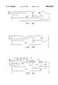
- FIG. 6Ais a sketch of a continuous MCT film having a compositional gradient in the film thickness direction (produced by any means) which has been lapped with a diamond point turning machine to convert the MCT film to an IR filter which has different wavelength responses in the lateral direction;
- FIG. 6Bsketches the formation of MCT detectors over the filter of FIG. 6A by means of conventional photolithography after MCT film deposition
- FIG. 6Csketches the formation of MCT detectors over the filter of FIG. 6A through the use of a silicon dioxide mask which is applied and patterned prior to film deposition to inhibit MCT film growth;
- FIG. 7Ais a sketch of a substrate holder which allows the simultaneous deposition of MCT films of the same composition on both sides of one or more substrates;
- FIG. 7Billustrates the post deposition heat treatment of the double film of FIG. 7A to achieve a very long lateral IR filter having novel response characteristics
- FIG. 8is a sketch illustrating the patterning of one of the heat treated double MCT films of FIG. 7A into discrete IR detectors which are displaced laterally at the chosen wavelengths with a width selected for the desired bandwidth;
- FIG. 9Aillustrates the use of GaAs as a lattice match material between MCT and Si to provide a material with active elements to process the signals from MCT detectors;
- FIG. 9Billustrates the use of zinc selenide (ZnSe) as a lattice match material between MCT and Si to provide a material with active elements to process the signals from MCT detectors;
- ZnSezinc selenide
- FIG. 9Cillustrates the use of a latterly continuously graded HgCdTe filter over MCT detectors; and FIGS. 9D-E illustrate rapid thermal annealing lamps used in conjunction with a reflective mask to provide non-uniform heating.
- FIG. 1is a graph of a model of the IR transmission (%) versus wavenumber (cm -1 ) for the MCT film composition (Hg.sub.(1-x) Cd x )Te.
- the IR wavelength in mmis -10 4 divided by the wavenumber.
- x0.3.
- x0.25.
- x0.2.
- the abscissa of the graphruns from a wavenumber of -3500 (corresponding to a wavelength of 2.9 mm) to a wavenumber of -500 (corresponding to a wavelength of 20 mm.)
- the transmission percentages modeledare illustrative but less than actual because no anti-reflection coatings are assumed.
- the wavelengths 15 to the left of 10are absorbed by MCT film 10 and, if electrodes are attached, an increase in conductance of 10 may be detected when emission in the 15 spectral region illuminates the MCT film.
- wavelengths in regions 16, 17 and 18 which are longer than 4.0 mmmay be transmitted through film 10 and typically, no change of conductance in 10 occurs when illuminated at wavelengths longer than 4.0 mm within spectral regions 16, 17 and 18.
- FIG. 2illustrates the preferred and well known method of epitaxially growing superior MCT films having very low Hg vacancies using a liquid phase epitaxial (LPE) reactor.
- Table 1describes the key components and their function.
- a first embodimentis a method of varying the composition of a (Hg.sub.(1-x) Cd x Te film during LPE film growth makes use of the strong temperature dependence of the segregation coefficient of Cd in the MCT melt.
- FIG. 3illustrates an example of a temperature profile to perform this within the reactor illustrated in FIG. 2.
- the temperaturemay be held at T1, for example, 450° C., for a rolled period of time, for example 20 minutes, to time 36.
- the temperatureis linearly
- a second embodiment of the present inventionis a method of providing an MCT film compositional gradient through the film thickness is performed after film growth. This method makes use of the interdiffusion of Cd from the substrate into the MCT film.
- FIG. 4is sketched a diagram of the apparatus.
- An MCT film 40has been grown on substrate 42.
- the IR transparent substrate 42may be CdTe or cadmium-zinc-telluride (CdZnTe, for example.)
- the substrate 42is placed in contact with heater 43 which is at a raised temperature. This causes the Cd in the substrate 42 to interdiffuse into MCT film 40 such that the MCT composition next to the substrate contains more Cd than the surface of 40.
- the x in (Hg.sub.(1-x) Cd x )Te next to the substrateis larger so the wavelength of IR absorbed or detected at the substrate interface surface is shorter than at the top surface of the film. This is the desirable material profile for through the substrate 42 IR radiation detection because the longer IR wavelengths must pass through the material next to 42 to reach the material at the film surface which is sensitive to longer wavelengths.
- FIG. 5A third embodiment of the present invention is illustrated in FIG. 5 and Table 2, which
- the lateral variation in this embodimentmay be quite long, such as 10 cm, if desired, which is achieved by driving Cd into the MCT film from the substrate by interdiffusion.
- the desired x in a (Hg.sub.(1-x) Cd x )Te film 40 of (typically) uniform compositionis grown on IR transparent CdTe or CdZnTe substrate 42 as previously described. This ensemble is placed on heater 43 which has a controlled temperature gradient, for example, where portion 44 is hotter than portion 45. These temperatures are selected for the desired properties of the modified film 40.
- the heat treated MCT film 40 in zone 39has a larger x in the (Hg.sub.(1-x) Cd x )Te equation (more Cd) than does that of zone 41; as a result, the modified MCT film 40 will have a gradient of IR response for use in filters and detectors which varies from short wavelengths in zone 39 to longer wavelengths in zone 41 through the lateral dimension of 40.
- a physically long dimensioned IR filter/detectormay be achieved with any desired spectral response within the IR spectrum.
- FIG. 6Ashows an exaggerated wedge of MCT film 40 which has been lapped on surface 46 to form a film which has varying wavelength response in the lateral direction.
- the MCT film 40 and substrate 42are the same as described for FIG. 4.
- a method of delineating detectors having different spectral responsesis shown in FIGS. 6B and 6C.
- a continuous MCT film 53has been deposited over the lapped surface 46.
- Photoresist 47has been placed over film 53 and standard photolithography has been performed to produce detectors 48, 50 and 52, all of which have different bandwidths and spectral centers because of the varying composition through the thickness of MCT film 40.
- FIG. 6CAnother method, shown in FIG. 6C, of creating these same detectors uses a mask to shield areas of MCT film 40 during the LPE growth process.
- a continuous silicon dioxide (SiO 2 ) film 55is deposited over MCT film 40.
- This oxide 55is patterned into a mask by standard lithography to etch holes where the detectors are to be located leaving SiO 2 islands 54.
- the ensembleis placed in an LPE reactor and the MCT material for detectors 48, 50 and 52 is deposited.
- the SiO 2 islands 54prevents growth of MCT films by acting as an oxide mask.
- detector 48will detect only the longest wavelengths, over the range of the width of detector 48; detector 50 will detect a wider IR band (because of its wider geometry) at the middle wavelengths; and detector 52 will detect a narrow band of short IR wavelengths.
- FIG. 7Ais a sketch of a substrate holder 56 which holds an IR transparent substrate 42 such that both sides of 42 are exposed to the MCT vapor in the LPE reactor shown in FIG. 2.
- the rectangular substrate 42 and holder 56 shownis used as a typical example with the understanding that the opening to both 42 sides may be circular, square or any other desired two dimensional geometry and that the holder may be designed for a plurality of substrates rather than just one.
- a cross sectional view of the substrate 42 after it has been exposed to the MCT vaporis shown in FIG. 7B for MCT films 64 and 70 on substrate 42.
- heater 60is optional and may either supply a constant temperature or graded temperature surface.
- heater 60is shown as a radiant heater and heater 43 is shown as a conduction heater but the choice is governed by the film properties desired. In this example it is assumed that the average temperature is hotter within film 70 than within film 64. Therefore the Cd interdiffusion from substrate 42 will produce a higher concentration of Cd within zone 68 than 62 directly above it.
- the lateral direction in both MCT films 64 and 70contain a gradient of decreasing Cd from zone 62 to 66 and zone 68 to 72, respectively.
- the IR properties within zone 68attenuates or detects shorter wavelengths than the MCT material 62 directly opposite it through IR transparent substrate 42. Through the vertical direction of the two films this results in a narrow band of IR spectrum characteristics with zone 68 attenuating the shorter wavelengths, but passing higher wavelengths to be detected/filtered by zone 62 at only a slightly higher wavelength than zone 68 blocks.
- MCT films 64 and 70are LPE deposited and heat treated as described in FIG. 7B such that a point lying on MCT film 64 has slightly less Cd than the same lateral location on 70.
- Film 64is patterned into detectors 86, 88 and 90 (FIG. 8) with attached electrical conductors 80,92 and 82,94 and 84,96 respectively. An increase of conductance in these detectors occurs when irradiated with the proper wavelengths of IR.
- the lateral positions of detectors 86, 88 and 90determine the center of their IR spectral response.
- the physical widths of detectors 86, 88 and 90determine their bandwidths.
- the width of detector 86may detect wavelengths having lower limits from 3 mm on the left to 4.5 mm on the right and the composition of film 70 immediately opposite to detect 86 may pass wavelengths longer than 2.8 mm on the left and 4.3 mm on the right.
- detector 86may exhibit increases in conductance for only the band of 3 to 4.5 mm.
- Detector 88has a similarly tailored response at longer wavelengths with a narrower passband than detector 86.
- Detector 90has a very narrow range of IR wavelength response at a longer wavelength than either detectors 86 or 88 which is desirable when detecting carbon dioxide or carbon monoxide components during combustion of organic material in an atmospheric environment.
- a double sided filter/detector deviceis that a substantial inventory of double sided film material may be prepared in advance. Subsequently the MCT film 64 may be patterned to achieve an IR response tailored to the application.
- FIG. 9 and Table 5illustrate two methods of manufacturing active devices and MCT filters and detectors on the same substrate. Although only one MCT film is shown, it should be understood that a plurality of MCT films acting as either or both filters and detectors is possible because the MCT growth temperature of around 450° C. will not harm either unbonded GaAs or unbonded Si devices.
- FIG. 9illustrates two methods of manufacturing active devices and MCT filters and detectors on the same substrate. Although only one MCT film is shown, it should be understood that a plurality of MCT films acting as either or both filters and detectors is possible because the MCT growth temperature of around 450° C. will not harm either unbonded GaAs or unbonded Si devices.
- GaAs 106an epitaxially grown film of GaAs 106 is grown on Si substrate 110. Where it is desired to form Si devices in region 112, the GaAs is etched away. Region 112 is fabricated with either or both discrete and integrated Si devices and then covered with a protective layer, such as plasma deposited silicon nitride (not shown) while GaAs devices are created in the GaAs region 108. Both 106 and 110 are covered
- MCT 100may now be fabricated into detectors having the desired IR wavelength response without harm to the protected circuits 108 and 112.
- the protective layer 104may now be selectively removed and interconnecting bonding pads opened such that leads may be attached or deposited between 100, 108 and 112 for the final system configuration.
- FIG. 9Bshows a similar configuration where only Si devices are required.
- the Si substrate 110has silicon devices fabricated in region 112 as before and then covered overall with a protective layer of plasma deposited silicon nitride 104.
- the exposed area of Si 110matches the lattice parameters of ZnSe close enough to allow the epitaxial growth of ZnSe film 114.
- ZnSealso matches the lattice parameters of CdTe close enough to allow the epitaxial growth of CdTe film 102.
- the MCT detector/filter film 100is grown on 102 and patterned into the desired detector/filter geometries.
- Layer 104may be selectively removed to expose the bonding pads of 112 and the such that interconnection leads may be bonded between the Si devices of 112 and the detectors formed from 100.
- FIG. 9cshows an integrated device with HgCdTe filter, HgCdTe IR sensors, and silicon circuitry, which can be used, e.g., as a integrated spectrometer.
- Layer 104has been selectively removed to form a via to expose the bonding pads of 112.
- the MCT film 100(see FIG. 9b) has been patterned (e.g. photolithographically etched) to form MCT detector stripes 101, 121.
- Via conductor 116has been formed (e.g. from a metal such as aluminum) in the via and interconnection lead 118 has been used to connect sensor 121 to via conductor 116, thus connecting the Si devices of 112 and the detectors formed from 100.
- Interconnection lead 118may be from a metal such as aluminum, but is preferably HgTe, and lead 118 is patterned to cover only a small end portion of sensor 121 and to leave most of the sensor uncovered.
- a second lead(not shown) can be used to make a second contact at the opposite end of sensor 121.
- CdTe insulator 120has been LPE grown between and over the stripes and MCT filter film 122 LPE grown over the CdTe insulator.
- FIG. 9dshows an alternate embodiment in which non-uniform MCT filter film 122 is fabricated using a mask 124 and conventional rapid thermal annealing lamps 126.
- This embodimentcan be used in controlled atmosphere containing Hg vapor.
- the maskcontains large openings 128 to provide hotter portions of MCT filter film 122, small openings 130, to provide intermediate temperature portions of MCT filter film 122, and solid portions 132 to provide cooler portions of MCT filter film 122.
- a non-contact maskis utilized, and the lamp-mask spacing is not to scale, as the lamps are generally much further away than shown.
- While rapid thermal annealing lampshave previously been used to provide uniform heating, here the lamps are used in conjunction with a reflective mask to provide non-uniform heating. Note that while the mask is shown with holes, it could also be a patterned reflective coating on a transparent substrate. Note also such lamps can also be used in conjunction with a mask to provide nonuniform heating to MCT film 100 (see FIG. 9b) prior to the application of CdTe insulator 120, either before or after film 100 has been patterned to form MCT detector stripes (stripes 101, 121 as shown in FIG. 9c). Such nonuniform heating of film 100 or stripes 101, 121 can provide for MCT detectors having different spectral responses.
- FIG. 9eshows and alternate embodiment in which a controlled atmosphere containing Hg vapor is not used. Instead, the structure of FIG. 9c has been modified by adding a HgTe layer 132 over the MCT filter film 122. Again, non-uniform MCT filter film 122 is fabricated using mask 124 and conventional rapid thermal annealing lamps 126. Generally the HgTe layer is removed after the heating.
- This embodimentcan be used to provide an integrated IR detector assembly with a continuously graded HgCdTe filter layer without the use of a controlled atmosphere containing Hg vapor.
- Non-uniform heatingcould e.g., also be provided by a scanning laser.
- Various modifications and combinations of the illustrative embodiments, as well as other embodiments of the invention,will be apparent to persons skilled in the art upon reference to the description. It is therefore intended that the appended claims encompass any such modifications or embodiments.
Landscapes
- Engineering & Computer Science (AREA)
- Physics & Mathematics (AREA)
- General Physics & Mathematics (AREA)
- Condensed Matter Physics & Semiconductors (AREA)
- Manufacturing & Machinery (AREA)
- Computer Hardware Design (AREA)
- Microelectronics & Electronic Packaging (AREA)
- Power Engineering (AREA)
- Spectroscopy & Molecular Physics (AREA)
- Chemical & Material Sciences (AREA)
- Materials Engineering (AREA)
- Light Receiving Elements (AREA)
Abstract
Description
TABLE 1______________________________________ID# Description Function______________________________________20 Process chamberSeals process environment 21 Substrate and holder support Supports and rotates substrate for uniform film deposition.22 Substrate holder Supports substrate duringdeposition 23 CdTe or CdZnTe substrate Provides surface for epitaxially growing MCT.24 Stirrer Agitates HgCdTe melt 27 for controlled deposition onsubstrate 2325 Hg, Cd, Te vapor Provides Hg vapor rich environ- ment during growth of MCT film.26 Crucible Container for melt 2727 Melt Molten HgCdTe source for MCT film deposition.28 Chamber Heater Controls temperature of upper process chamber.29 Thermocouple well Monitors temperature ofchamber heater 28.______________________________________
TABLE 2______________________________________ID# Description Function______________________________________39 Zone of 40 having highest Cd Provides shortestIR wavelength response 40 Uniformly deposited MCT film Controls range of IR response desired41 Zone of 40 having lowest Cd Provides longestIR wavelength response 42 CdTe or CdZnTe substrate Provides a substrate with suitable lattice match to MCT for epitaxial growth and is transparent to the range of IR wavelengths desired.43 Heater Provides controlledtemperature gradient 44 Hotter portion ofheater 43 Interdiffuses more Cd per unit time intozone 4045 Cooler portion ofheater 43 Interdiffuses less Cd per unit time intozone 40______________________________________
TABLE 3______________________________________ID # Description Function______________________________________60 Radiant heater Provides control over difference of annealing temperatures between substrate surfaces.62 Hotter zone ofMCT film 64 Results in higher Cd concentration thanzone 66 but less than 68.64 MCT film of uniform Determines physical properties composition before heat treatment.66 Cooler zone ofMCT film 64 Results in lower Cd concentration than62 and 72.68 Hotter zone within MCT film Results in the zone highest Cd 70 concentration of any zone in either 64 or 70.70 Same asMCT film 64 on the other side of thesubstrate 42.72 Cooler zone than 68 but hotter Results in Cd concentration lower thanzone 66. thanzone 68 but higher than 66.______________________________________
TABLE 4______________________________________ID# Description Function______________________________________42 CdTe or CdZnTe Provide a substrate with suitable lattice substrate match to MCT for epitaxial growth and be transparent to the range of IR wavelengths desired.64 Heat treated MCT film as Achieve IR response related to described in FIG.7B MCT film 70.68 Highest Cd composition Attenuate lower and pass higher of 70. wavelengths of IR spectrum.70 Heat treated MCT film as Achieve IR response related to described in FIG.7B MCT film 68.72 Lowest Cd composition Attenuate longer IR wavelengths of 70. but pass those which will be detected immediately above bydetector 90.86 Detectors; Patterned portions offilm 64 Form wideband IR detector for shorter IR wavelengths.80, Electrical contacts Forms electrical connection for external92, to detector 86 electronics to detect changes of93 conductance of 86 with IR radiation.88 Patterned portion of Form medium bandwidth IR detector atfilm 64 medium wavelengths of IR spectrum.82, 9 Electrical contacts Forms electrical connection for external4, 95 todetector 88 electronics to detect changes of conductance of 88 with IR radiation.90 Patterned portion Form very narrow bandwidth, long offilm 64 wavelength IR detector.84, 9 Electrical contacts Forms electrical connection for external6, 97 todetector 90 electronics to detect changes of conductance of 90 with IR radiation.98 Incident IR radiation______________________________________
TABLE 5______________________________________ID# Description Function______________________________________100 MCT film layer To be patterned intoIR detectors 102 CdTe film layer Lattice match between 100 and 106 permits LPE film growth.104 Plasma deposited silicon nitride Prevents damage toregions 108 or silicon oxide protective layer and 112 which contain active semiconductor devices.106 GaAs epitaxial layer Can be epitaxially grown on Si and can also provide useful devices within 108.108 Protected GaAs device region May contain discrete or inte- grated circuit devices of GaAs.110 Silicon substrate Provides mechanical support for all epitaxially grown layers and may provideregion 112.112 Protected Si device region May contain discrete or inte- grated circuit devices of Si.114 ZnSe epitaxial layer Provides lattice parameters which allows it to be epitaxially grown on Si and also allows CdTe to be epitaxially grown on it.______________________________________
Claims (17)
Priority Applications (1)
| Application Number | Priority Date | Filing Date | Title |
|---|---|---|---|
| US08/831,170US5861626A (en) | 1996-04-04 | 1997-04-02 | Mercury cadmium telluride infrared filters and detectors and methods of fabrication |
Applications Claiming Priority (2)
| Application Number | Priority Date | Filing Date | Title |
|---|---|---|---|
| US1487396P | 1996-04-04 | 1996-04-04 | |
| US08/831,170US5861626A (en) | 1996-04-04 | 1997-04-02 | Mercury cadmium telluride infrared filters and detectors and methods of fabrication |
Publications (1)
| Publication Number | Publication Date |
|---|---|
| US5861626Atrue US5861626A (en) | 1999-01-19 |
Family
ID=26686644
Family Applications (1)
| Application Number | Title | Priority Date | Filing Date |
|---|---|---|---|
| US08/831,170Expired - LifetimeUS5861626A (en) | 1996-04-04 | 1997-04-02 | Mercury cadmium telluride infrared filters and detectors and methods of fabrication |
Country Status (1)
| Country | Link |
|---|---|
| US (1) | US5861626A (en) |
Cited By (16)
| Publication number | Priority date | Publication date | Assignee | Title |
|---|---|---|---|---|
| US6036770A (en)* | 1996-04-04 | 2000-03-14 | Raytheon Company | Method of fabricating a laterally continuously graded mercury cadmium telluride layer |
| US6091127A (en)* | 1997-04-02 | 2000-07-18 | Raytheon Company | Integrated infrared detection system |
| WO2001040777A1 (en)* | 1999-12-01 | 2001-06-07 | Deutsche Telekom Ag | Optical spectroscopy device and method for the production thereof |
| US20020179839A1 (en)* | 2001-06-04 | 2002-12-05 | Isaac Richman | Detector array structure for eliminating channel spectrum |
| RU2310949C1 (en)* | 2006-08-03 | 2007-11-20 | Институт физики полупроводников Сибирского отделения Российской академии наук | Photodiode infrared detector |
| US20080315342A1 (en)* | 2005-12-21 | 2008-12-25 | Durham Scientific Crystals Limited | Semiconductor Device with a Bulk Single Crystal on a Substrate |
| US20090053453A1 (en)* | 2005-12-21 | 2009-02-26 | Durham Scientific Crystals Limited | Semiconductor device and method of manufacture thereof |
| CN102117861B (en)* | 2009-12-30 | 2012-07-25 | 昆明物理研究所 | Method for manufacturing amorphous mercury cadmium telluride monolithic integrated focal plane detector |
| US20130005068A1 (en)* | 2011-06-30 | 2013-01-03 | Centre National De La Recherche Scientifique | Method for manufacturing an electromagnetic radiation detector and detector obtained by such a method |
| CN102117816B (en)* | 2009-12-30 | 2013-03-06 | 昆明物理研究所 | Amorphous HgCdTe monolithic integrated type focal plane detector |
| RU2529457C1 (en)* | 2013-07-17 | 2014-09-27 | Федеральное государственное бюджетное образовательное учреждение высшего профессионального образования "Национальный исследовательский Томский государственный университет" (ТГУ) | Infrared photosensitive structure and method of making same |
| FR3042310A1 (en)* | 2015-10-12 | 2017-04-14 | Commissariat Energie Atomique | MANUFACTURE OF A MULTISPECTRAL PHOTODIOD MATRIX IN CDHGTE BY CADMIUM DIFFUSION |
| US9899547B2 (en) | 2016-04-25 | 2018-02-20 | International Business Machines Corporation | Multi-wavelength detector array incorporating two dimensional and one dimensional materials |
| CN110873605A (en)* | 2018-08-31 | 2020-03-10 | 三星电子株式会社 | Optical filter and spectrometer including optical filter |
| WO2022090106A1 (en) | 2020-10-26 | 2022-05-05 | Trinamix Gmbh | Optical detector and method for determining at least one property of at least one substance |
| WO2023004166A1 (en)* | 2021-07-23 | 2023-01-26 | Board Of Regents Of The Nevada System Of Higher Education, On Behalf Of The Univ. Of Nevada | Photoacoustic spectrometer for real-time dust monitoring |
Citations (14)
| Publication number | Priority date | Publication date | Assignee | Title |
|---|---|---|---|---|
| US4296324A (en)* | 1979-11-02 | 1981-10-20 | Santa Barbara Research Center | Dual spectrum infrared fire sensor |
| US4370557A (en)* | 1980-08-27 | 1983-01-25 | Honeywell Inc. | Dual detector flame sensor |
| US4376659A (en)* | 1981-06-01 | 1983-03-15 | Texas Instruments Incorporated | Process for forming semiconductor alloys having a desired bandgap |
| US4691196A (en)* | 1984-03-23 | 1987-09-01 | Santa Barbara Research Center | Dual spectrum frequency responding fire sensor |
| US4769775A (en)* | 1981-05-21 | 1988-09-06 | Santa Barbara Research Center | Microprocessor-controlled fire sensor |
| US4965649A (en)* | 1988-12-23 | 1990-10-23 | Ford Aerospace Corporation | Manufacture of monolithic infrared focal plane arrays |
| US5302232A (en)* | 1992-01-31 | 1994-04-12 | Fujitsu Limited | (111) Group II-VI epitaxial layer grown on (111) silicon substrate |
| US5449927A (en)* | 1994-05-16 | 1995-09-12 | Santa Barbara Research Center | Multilayer buffer structure including II-VI compounds on a silicon substrate |
| US5459321A (en)* | 1990-12-26 | 1995-10-17 | The United States Of America As Represented By The Secretary Of The Navy | Laser hardened backside illuminated optical detector |
| US5479018A (en)* | 1989-05-08 | 1995-12-26 | Westinghouse Electric Corp. | Back surface illuminated infrared detector |
| US5510644A (en)* | 1992-03-23 | 1996-04-23 | Martin Marietta Corporation | CDTE x-ray detector for use at room temperature |
| US5559336A (en)* | 1994-07-05 | 1996-09-24 | Santa Barbara Research Center | Integrated LPE-grown structure for simultaneous detection of infrared radiation in two bands |
| US5581117A (en)* | 1994-12-13 | 1996-12-03 | Nec Corporation | Si base substrate covered by a CdTe or Cd-rich CdZnTe layer |
| US5633527A (en)* | 1995-02-06 | 1997-05-27 | Sandia Corporation | Unitary lens semiconductor device |
- 1997
- 1997-04-02USUS08/831,170patent/US5861626A/ennot_activeExpired - Lifetime
Patent Citations (15)
| Publication number | Priority date | Publication date | Assignee | Title |
|---|---|---|---|---|
| US4296324A (en)* | 1979-11-02 | 1981-10-20 | Santa Barbara Research Center | Dual spectrum infrared fire sensor |
| US4370557A (en)* | 1980-08-27 | 1983-01-25 | Honeywell Inc. | Dual detector flame sensor |
| US4769775A (en)* | 1981-05-21 | 1988-09-06 | Santa Barbara Research Center | Microprocessor-controlled fire sensor |
| US4376659A (en)* | 1981-06-01 | 1983-03-15 | Texas Instruments Incorporated | Process for forming semiconductor alloys having a desired bandgap |
| US4691196A (en)* | 1984-03-23 | 1987-09-01 | Santa Barbara Research Center | Dual spectrum frequency responding fire sensor |
| US4785292A (en)* | 1984-03-23 | 1988-11-15 | Santa Barbara Research Center | Dual spectrum frequency responding fire sensor |
| US4965649A (en)* | 1988-12-23 | 1990-10-23 | Ford Aerospace Corporation | Manufacture of monolithic infrared focal plane arrays |
| US5479018A (en)* | 1989-05-08 | 1995-12-26 | Westinghouse Electric Corp. | Back surface illuminated infrared detector |
| US5459321A (en)* | 1990-12-26 | 1995-10-17 | The United States Of America As Represented By The Secretary Of The Navy | Laser hardened backside illuminated optical detector |
| US5302232A (en)* | 1992-01-31 | 1994-04-12 | Fujitsu Limited | (111) Group II-VI epitaxial layer grown on (111) silicon substrate |
| US5510644A (en)* | 1992-03-23 | 1996-04-23 | Martin Marietta Corporation | CDTE x-ray detector for use at room temperature |
| US5449927A (en)* | 1994-05-16 | 1995-09-12 | Santa Barbara Research Center | Multilayer buffer structure including II-VI compounds on a silicon substrate |
| US5559336A (en)* | 1994-07-05 | 1996-09-24 | Santa Barbara Research Center | Integrated LPE-grown structure for simultaneous detection of infrared radiation in two bands |
| US5581117A (en)* | 1994-12-13 | 1996-12-03 | Nec Corporation | Si base substrate covered by a CdTe or Cd-rich CdZnTe layer |
| US5633527A (en)* | 1995-02-06 | 1997-05-27 | Sandia Corporation | Unitary lens semiconductor device |
Non-Patent Citations (2)
| Title |
|---|
| T. Ting, Journal of Crystal Growth, (Netherlands), vol. 86, pp.161 172 (1988).* |
| T. Ting, Journal of Crystal Growth,(Netherlands), vol. 86, pp.161-172 (1988). |
Cited By (29)
| Publication number | Priority date | Publication date | Assignee | Title |
|---|---|---|---|---|
| US6140145A (en)* | 1996-04-04 | 2000-10-31 | Raytheon Company | Integrated infrared detection system |
| US6036770A (en)* | 1996-04-04 | 2000-03-14 | Raytheon Company | Method of fabricating a laterally continuously graded mercury cadmium telluride layer |
| US6091127A (en)* | 1997-04-02 | 2000-07-18 | Raytheon Company | Integrated infrared detection system |
| US8868156B1 (en) | 1999-12-01 | 2014-10-21 | Deutsche Telekom Ag | Optical spectroscopy device and method for its manufacture |
| WO2001040777A1 (en)* | 1999-12-01 | 2001-06-07 | Deutsche Telekom Ag | Optical spectroscopy device and method for the production thereof |
| US20020179839A1 (en)* | 2001-06-04 | 2002-12-05 | Isaac Richman | Detector array structure for eliminating channel spectrum |
| US6573505B2 (en)* | 2001-06-04 | 2003-06-03 | The Boeing Company | Detector array structure for eliminating channel spectrum |
| US20090053453A1 (en)* | 2005-12-21 | 2009-02-26 | Durham Scientific Crystals Limited | Semiconductor device and method of manufacture thereof |
| US20080315342A1 (en)* | 2005-12-21 | 2008-12-25 | Durham Scientific Crystals Limited | Semiconductor Device with a Bulk Single Crystal on a Substrate |
| US20100327277A1 (en)* | 2005-12-21 | 2010-12-30 | Durham Scientific Crystals Limited | Semiconductor device with a bulk single crystal on a substrate |
| US20110024877A1 (en)* | 2005-12-21 | 2011-02-03 | Durham Scientific Crystals Limited | Semiconductor device and method of manufacture thereof |
| US8093671B2 (en) | 2005-12-21 | 2012-01-10 | Kromek Limited | Semiconductor device with a bulk single crystal on a substrate |
| US8093095B2 (en) | 2005-12-21 | 2012-01-10 | Kromek Limited | Semiconductor device with a bulk single crystal on a substrate |
| US8968469B2 (en) | 2005-12-21 | 2015-03-03 | Kromek Limited | Semiconductor device and method of manufacture thereof |
| RU2310949C1 (en)* | 2006-08-03 | 2007-11-20 | Институт физики полупроводников Сибирского отделения Российской академии наук | Photodiode infrared detector |
| CN102117861B (en)* | 2009-12-30 | 2012-07-25 | 昆明物理研究所 | Method for manufacturing amorphous mercury cadmium telluride monolithic integrated focal plane detector |
| CN102117816B (en)* | 2009-12-30 | 2013-03-06 | 昆明物理研究所 | Amorphous HgCdTe monolithic integrated type focal plane detector |
| US20130005068A1 (en)* | 2011-06-30 | 2013-01-03 | Centre National De La Recherche Scientifique | Method for manufacturing an electromagnetic radiation detector and detector obtained by such a method |
| US8900907B2 (en)* | 2011-06-30 | 2014-12-02 | Societe Francaise De Detecteurs Infrarouges-Sofradir | Method for manufacturing an electromagnetic radiation detector and detector obtained by a growth substrate removal method |
| RU2529457C1 (en)* | 2013-07-17 | 2014-09-27 | Федеральное государственное бюджетное образовательное учреждение высшего профессионального образования "Национальный исследовательский Томский государственный университет" (ТГУ) | Infrared photosensitive structure and method of making same |
| FR3042310A1 (en)* | 2015-10-12 | 2017-04-14 | Commissariat Energie Atomique | MANUFACTURE OF A MULTISPECTRAL PHOTODIOD MATRIX IN CDHGTE BY CADMIUM DIFFUSION |
| EP3157067A1 (en)* | 2015-10-12 | 2017-04-19 | Commissariat à l'Energie Atomique et aux Energies Alternatives | Manufacturing of a cdhgte multispectral photodiode array through cadmium diffusion |
| US10079263B2 (en) | 2015-10-12 | 2018-09-18 | Commissariat A L'energie Atomique Et Aux Energies Alternatives | Manufacture of a CdHgTe multispectral photodiode array by cadmium diffusion |
| US9899547B2 (en) | 2016-04-25 | 2018-02-20 | International Business Machines Corporation | Multi-wavelength detector array incorporating two dimensional and one dimensional materials |
| US10069028B2 (en) | 2016-04-25 | 2018-09-04 | International Business Machines Corporation | Multi-wavelength detector array incorporating two dimensional and one dimensional materials |
| US10388805B2 (en) | 2016-04-25 | 2019-08-20 | International Business Machines Corporation | Multi-wavelength detector array incorporating two dimensional and one dimensional materials |
| CN110873605A (en)* | 2018-08-31 | 2020-03-10 | 三星电子株式会社 | Optical filter and spectrometer including optical filter |
| WO2022090106A1 (en) | 2020-10-26 | 2022-05-05 | Trinamix Gmbh | Optical detector and method for determining at least one property of at least one substance |
| WO2023004166A1 (en)* | 2021-07-23 | 2023-01-26 | Board Of Regents Of The Nevada System Of Higher Education, On Behalf Of The Univ. Of Nevada | Photoacoustic spectrometer for real-time dust monitoring |
Similar Documents
| Publication | Publication Date | Title |
|---|---|---|
| US5861626A (en) | Mercury cadmium telluride infrared filters and detectors and methods of fabrication | |
| US6770882B2 (en) | Micromachined pyro-optical structure | |
| US5367167A (en) | Uncooled infrared detector and method for forming the same | |
| US6091127A (en) | Integrated infrared detection system | |
| US5021663A (en) | Infrared detector | |
| EP0354369B1 (en) | Infrared detector | |
| US6392232B1 (en) | High fill factor bolometer array | |
| US5777329A (en) | Bolometer array spectrometer | |
| US5777328A (en) | Ramped foot support | |
| EP0534768B1 (en) | Uncooled infrared detector and method for forming the same | |
| USRE36706E (en) | Microstructure design for high IR sensitivity | |
| US6756594B2 (en) | Micromachined tuned-band hot bolometer emitter | |
| EP0177918B1 (en) | Uv detector and method for fabricating it | |
| US6028312A (en) | Electronic chopping | |
| US5789753A (en) | Stress tolerant bolometer | |
| US5841137A (en) | Duplicative detector sensor | |
| US20070034978A1 (en) | Photonic crystal emitter, detector and sensor | |
| US6064066A (en) | Bolometer autocalibration | |
| KR100444638B1 (en) | Reflective semiconductor substrate | |
| US20150098481A1 (en) | Optical signal amplification | |
| US5406081A (en) | Infrared detector utilizing diamond film | |
| US6036770A (en) | Method of fabricating a laterally continuously graded mercury cadmium telluride layer | |
| WO1994001743A1 (en) | Microstructure design for high ir sensitivity | |
| RU2208268C2 (en) | Semiconductor infrared radiator | |
| EP0773435A2 (en) | Method and devices for measuring radiation |
Legal Events
| Date | Code | Title | Description |
|---|---|---|---|
| AS | Assignment | Owner name:TEXAS INSTRUMENTS INCORPORATED, TEXAS Free format text:ASSIGNMENT OF ASSIGNORS INTEREST;ASSIGNORS:CHANDRA, DIPANKAR;WEIRAUCH, DONALD F.;PENN, THOMAS C.;REEL/FRAME:008752/0545;SIGNING DATES FROM 19970911 TO 19970918 | |
| AS | Assignment | Owner name:RAYTHEON TI SYSTEMS, INC., A CORP. OF DELAWARE, TE Free format text:ASSIGNMENT OF ASSIGNORS INTEREST;ASSIGNOR:TEXAS INSTRUMENTS INCORPORATED, A CORP. OF DELAWARE;REEL/FRAME:008764/0244 Effective date:19970924 | |
| STCF | Information on status: patent grant | Free format text:PATENTED CASE | |
| AS | Assignment | Owner name:RAYTHEON COMPANY, A CORPORATION OF DELAWARE, MASSA Free format text:CHANGE OF NAME;ASSIGNOR:RAYTHEON TI SYSTEMS, INC.;REEL/FRAME:009875/0499 Effective date:19981229 | |
| CC | Certificate of correction | ||
| FEPP | Fee payment procedure | Free format text:PAYOR NUMBER ASSIGNED (ORIGINAL EVENT CODE: ASPN); ENTITY STATUS OF PATENT OWNER: LARGE ENTITY | |
| FPAY | Fee payment | Year of fee payment:4 | |
| FPAY | Fee payment | Year of fee payment:8 | |
| FEPP | Fee payment procedure | Free format text:PAYER NUMBER DE-ASSIGNED (ORIGINAL EVENT CODE: RMPN); ENTITY STATUS OF PATENT OWNER: LARGE ENTITY Free format text:PAYOR NUMBER ASSIGNED (ORIGINAL EVENT CODE: ASPN); ENTITY STATUS OF PATENT OWNER: LARGE ENTITY | |
| FPAY | Fee payment | Year of fee payment:12 | |
| AS | Assignment | Owner name:OL SECURITY LIMITED LIABILITY COMPANY, DELAWARE Free format text:ASSIGNMENT OF ASSIGNORS INTEREST;ASSIGNOR:RAYTHEON COMPANY;REEL/FRAME:029117/0335 Effective date:20120730 | |
| FEPP | Fee payment procedure | Free format text:PAYER NUMBER DE-ASSIGNED (ORIGINAL EVENT CODE: RMPN); ENTITY STATUS OF PATENT OWNER: LARGE ENTITY Free format text:PAYOR NUMBER ASSIGNED (ORIGINAL EVENT CODE: ASPN); ENTITY STATUS OF PATENT OWNER: LARGE ENTITY | |
| AS | Assignment | Owner name:RAYTHEON COMPANY, MASSACHUSETTS Free format text:CORRECTIVE ASSIGNMENT TO CORRECT THE NATURE OF CONVEYANCE MARKED ON THE RECORDATION COVER SHEET PREVIOUSLY RECORDED ON REEL 009875 FRAME 0499. ASSIGNOR(S) HEREBY CONFIRMS THE NATURE OF CONVEYANCE IS A MERGER DOCUMENT;ASSIGNOR:RAYTHEON TI SYSTEMS, INC.;REEL/FRAME:029554/0291 Effective date:19981229 | |
| AS | Assignment | Owner name:HANGER SOLUTIONS, LLC, GEORGIA Free format text:ASSIGNMENT OF ASSIGNORS INTEREST;ASSIGNOR:INTELLECTUAL VENTURES ASSETS 158 LLC;REEL/FRAME:051486/0425 Effective date:20191206 | |
| AS | Assignment | Owner name:INTELLECTUAL VENTURES ASSETS 158 LLC, DELAWARE Free format text:ASSIGNMENT OF ASSIGNORS INTEREST;ASSIGNOR:OL SECURITY LIMITED LIABILITY COMPANY;REEL/FRAME:051846/0192 Effective date:20191126 |