US5859754A - Magnetoresistive transducer having a common magnetic bias using assertive and complementary signals - Google Patents
Magnetoresistive transducer having a common magnetic bias using assertive and complementary signalsDownload PDFInfo
- Publication number
- US5859754A US5859754AUS08/833,058US83305897AUS5859754AUS 5859754 AUS5859754 AUS 5859754AUS 83305897 AUS83305897 AUS 83305897AUS 5859754 AUS5859754 AUS 5859754A
- Authority
- US
- United States
- Prior art keywords
- layer
- transducer
- assertive
- ferromagnetic material
- complementary
- Prior art date
- Legal status (The legal status is an assumption and is not a legal conclusion. Google has not performed a legal analysis and makes no representation as to the accuracy of the status listed.)
- Expired - Lifetime
Links
- 230000005291magnetic effectEffects0.000titleclaimsabstractdescription64
- 230000000295complement effectEffects0.000titleclaimsabstractdescription44
- 230000005290antiferromagnetic effectEffects0.000claimsabstractdescription16
- 230000005415magnetizationEffects0.000claimsdescription37
- 230000004907fluxEffects0.000claimsdescription30
- 230000005294ferromagnetic effectEffects0.000claimsdescription29
- 239000003302ferromagnetic materialSubstances0.000claimsdescription28
- 239000002885antiferromagnetic materialSubstances0.000claimsdescription18
- PXHVJJICTQNCMI-UHFFFAOYSA-NNickelChemical compound[Ni]PXHVJJICTQNCMI-UHFFFAOYSA-N0.000claimsdescription8
- 230000004044responseEffects0.000claimsdescription7
- 239000010409thin filmSubstances0.000claimsdescription7
- 239000004020conductorSubstances0.000claimsdescription5
- 229910001030Iron–nickel alloyInorganic materials0.000claimsdescription3
- 229910045601alloyInorganic materials0.000claims3
- 239000000956alloySubstances0.000claims3
- 239000010941cobaltSubstances0.000claims3
- 229910017052cobaltInorganic materials0.000claims3
- GUTLYIVDDKVIGB-UHFFFAOYSA-Ncobalt atomChemical compound[Co]GUTLYIVDDKVIGB-UHFFFAOYSA-N0.000claims3
- 229910052759nickelInorganic materials0.000claims3
- 125000006850spacer groupChemical group0.000description11
- 239000000463materialSubstances0.000description10
- 230000008859changeEffects0.000description9
- 238000000034methodMethods0.000description9
- 230000008569processEffects0.000description8
- 230000008878couplingEffects0.000description7
- 238000010168coupling processMethods0.000description7
- 238000005859coupling reactionMethods0.000description7
- 239000013598vectorSubstances0.000description6
- 238000013461designMethods0.000description5
- 150000002500ionsChemical group0.000description5
- 238000004519manufacturing processMethods0.000description5
- 239000000758substrateSubstances0.000description5
- 230000000694effectsEffects0.000description4
- 230000006870functionEffects0.000description4
- UQSXHKLRYXJYBZ-UHFFFAOYSA-Niron oxideInorganic materials[Fe]=OUQSXHKLRYXJYBZ-UHFFFAOYSA-N0.000description4
- 238000012216screeningMethods0.000description4
- 239000010949copperSubstances0.000description3
- 239000010931goldSubstances0.000description3
- 230000005381magnetic domainEffects0.000description3
- 230000002459sustained effectEffects0.000description3
- 230000005330Barkhausen effectEffects0.000description2
- 229910000531Co alloyInorganic materials0.000description2
- RYGMFSIKBFXOCR-UHFFFAOYSA-NCopperChemical compound[Cu]RYGMFSIKBFXOCR-UHFFFAOYSA-N0.000description2
- 229910017344Fe2 O3Inorganic materials0.000description2
- BQCADISMDOOEFD-UHFFFAOYSA-NSilverChemical compound[Ag]BQCADISMDOOEFD-UHFFFAOYSA-N0.000description2
- 235000002017Zea mays subsp maysNutrition0.000description2
- 241000482268Zea mays subsp. maysSpecies0.000description2
- 239000000919ceramicSubstances0.000description2
- 229910052802copperInorganic materials0.000description2
- 238000010586diagramMethods0.000description2
- PCHJSUWPFVWCPO-UHFFFAOYSA-NgoldChemical compound[Au]PCHJSUWPFVWCPO-UHFFFAOYSA-N0.000description2
- 229910052737goldInorganic materials0.000description2
- 239000012212insulatorSubstances0.000description2
- 239000000696magnetic materialSubstances0.000description2
- 229910000480nickel oxideInorganic materials0.000description2
- NDLPOXTZKUMGOV-UHFFFAOYSA-Noxo(oxoferriooxy)iron hydrateChemical compoundO.O=[Fe]O[Fe]=ONDLPOXTZKUMGOV-UHFFFAOYSA-N0.000description2
- 230000035699permeabilityEffects0.000description2
- 238000012545processingMethods0.000description2
- 230000035945sensitivityEffects0.000description2
- 230000008054signal transmissionEffects0.000description2
- 229910052709silverInorganic materials0.000description2
- 239000004332silverSubstances0.000description2
- 229910018404Al2 O3Inorganic materials0.000description1
- CWYNVVGOOAEACU-UHFFFAOYSA-NFe2+Chemical compound[Fe+2]CWYNVVGOOAEACU-UHFFFAOYSA-N0.000description1
- PWHULOQIROXLJO-UHFFFAOYSA-NManganeseChemical compound[Mn]PWHULOQIROXLJO-UHFFFAOYSA-N0.000description1
- 229910052779NeodymiumInorganic materials0.000description1
- 229910000990Ni alloyInorganic materials0.000description1
- QXZUUHYBWMWJHK-UHFFFAOYSA-N[Co].[Ni]Chemical compound[Co].[Ni]QXZUUHYBWMWJHK-UHFFFAOYSA-N0.000description1
- 238000009825accumulationMethods0.000description1
- PNEYBMLMFCGWSK-UHFFFAOYSA-Naluminium oxideInorganic materials[O-2].[O-2].[O-2].[Al+3].[Al+3]PNEYBMLMFCGWSK-UHFFFAOYSA-N0.000description1
- 230000008901benefitEffects0.000description1
- 239000002131composite materialSubstances0.000description1
- 239000002772conduction electronSubstances0.000description1
- 230000003247decreasing effectEffects0.000description1
- 230000001939inductive effectEffects0.000description1
- 229910052748manganeseInorganic materials0.000description1
- 239000011572manganeseSubstances0.000description1
- 230000007246mechanismEffects0.000description1
- 230000004048modificationEffects0.000description1
- 238000012986modificationMethods0.000description1
- QEFYFXOXNSNQGX-UHFFFAOYSA-Nneodymium atomChemical compound[Nd]QEFYFXOXNSNQGX-UHFFFAOYSA-N0.000description1
- GNRSAWUEBMWBQH-UHFFFAOYSA-NoxonickelChemical compound[Ni]=OGNRSAWUEBMWBQH-UHFFFAOYSA-N0.000description1
- 229910000889permalloyInorganic materials0.000description1
- 230000008707rearrangementEffects0.000description1
- 230000009467reductionEffects0.000description1
- 230000002787reinforcementEffects0.000description1
- 230000007704transitionEffects0.000description1
Images


Classifications
- B—PERFORMING OPERATIONS; TRANSPORTING
- B82—NANOTECHNOLOGY
- B82Y—SPECIFIC USES OR APPLICATIONS OF NANOSTRUCTURES; MEASUREMENT OR ANALYSIS OF NANOSTRUCTURES; MANUFACTURE OR TREATMENT OF NANOSTRUCTURES
- B82Y25/00—Nanomagnetism, e.g. magnetoimpedance, anisotropic magnetoresistance, giant magnetoresistance or tunneling magnetoresistance
- G—PHYSICS
- G01—MEASURING; TESTING
- G01R—MEASURING ELECTRIC VARIABLES; MEASURING MAGNETIC VARIABLES
- G01R33/00—Arrangements or instruments for measuring magnetic variables
- G01R33/02—Measuring direction or magnitude of magnetic fields or magnetic flux
- G01R33/06—Measuring direction or magnitude of magnetic fields or magnetic flux using galvano-magnetic devices
- G01R33/09—Magnetoresistive devices
- G01R33/093—Magnetoresistive devices using multilayer structures, e.g. giant magnetoresistance sensors
- B—PERFORMING OPERATIONS; TRANSPORTING
- B82—NANOTECHNOLOGY
- B82Y—SPECIFIC USES OR APPLICATIONS OF NANOSTRUCTURES; MEASUREMENT OR ANALYSIS OF NANOSTRUCTURES; MANUFACTURE OR TREATMENT OF NANOSTRUCTURES
- B82Y10/00—Nanotechnology for information processing, storage or transmission, e.g. quantum computing or single electron logic
- G—PHYSICS
- G01—MEASURING; TESTING
- G01R—MEASURING ELECTRIC VARIABLES; MEASURING MAGNETIC VARIABLES
- G01R33/00—Arrangements or instruments for measuring magnetic variables
- G01R33/02—Measuring direction or magnitude of magnetic fields or magnetic flux
- G01R33/06—Measuring direction or magnitude of magnetic fields or magnetic flux using galvano-magnetic devices
- G01R33/09—Magnetoresistive devices
- G01R33/096—Magnetoresistive devices anisotropic magnetoresistance sensors
- G—PHYSICS
- G11—INFORMATION STORAGE
- G11B—INFORMATION STORAGE BASED ON RELATIVE MOVEMENT BETWEEN RECORD CARRIER AND TRANSDUCER
- G11B5/00—Recording by magnetisation or demagnetisation of a record carrier; Reproducing by magnetic means; Record carriers therefor
- G11B5/127—Structure or manufacture of heads, e.g. inductive
- G11B5/33—Structure or manufacture of flux-sensitive heads, i.e. for reproduction only; Combination of such heads with means for recording or erasing only
- G11B5/39—Structure or manufacture of flux-sensitive heads, i.e. for reproduction only; Combination of such heads with means for recording or erasing only using magneto-resistive devices or effects
- G11B5/3903—Structure or manufacture of flux-sensitive heads, i.e. for reproduction only; Combination of such heads with means for recording or erasing only using magneto-resistive devices or effects using magnetic thin film layers or their effects, the films being part of integrated structures
- G11B5/3906—Details related to the use of magnetic thin film layers or to their effects
- G11B5/3945—Heads comprising more than one sensitive element
- G11B5/3948—Heads comprising more than one sensitive element the sensitive elements being active read-out elements
- G11B5/3951—Heads comprising more than one sensitive element the sensitive elements being active read-out elements the active elements being arranged on several parallel planes
- G11B5/3954—Heads comprising more than one sensitive element the sensitive elements being active read-out elements the active elements being arranged on several parallel planes the active elements transducing on a single track
- G—PHYSICS
- G11—INFORMATION STORAGE
- G11B—INFORMATION STORAGE BASED ON RELATIVE MOVEMENT BETWEEN RECORD CARRIER AND TRANSDUCER
- G11B5/00—Recording by magnetisation or demagnetisation of a record carrier; Reproducing by magnetic means; Record carriers therefor
- G11B5/127—Structure or manufacture of heads, e.g. inductive
- G11B5/33—Structure or manufacture of flux-sensitive heads, i.e. for reproduction only; Combination of such heads with means for recording or erasing only
- G11B5/39—Structure or manufacture of flux-sensitive heads, i.e. for reproduction only; Combination of such heads with means for recording or erasing only using magneto-resistive devices or effects
- G11B2005/3996—Structure or manufacture of flux-sensitive heads, i.e. for reproduction only; Combination of such heads with means for recording or erasing only using magneto-resistive devices or effects large or giant magnetoresistive effects [GMR], e.g. as generated in spin-valve [SV] devices
Definitions
- This inventionrelates to magnetic read transducers capable of converting magnetic flux changes sensed from recorded media into assertive and complementary electrical signals.
- Inductive magnetic headsare commonly employed to perform recording and reading of data.
- the constant demand for high recording density disk drives with smaller physical sizes, higher storage capacities and better performancerequires manufacturers to build recording components that are capable of storing data with decreased data track widths and increased linear recording densities. This poses technical problems in the design and manufacture of magnetic transducers.
- Magnetoresistive (MR) headscan read information on a record medium with much narrower data track widths and yield improved signal-to-noise ratio.
- the output signal generated during the data reading processis independent of the traveling speed of the recording medium.
- a typical MR headincludes an MR sensor sandwiched between two magnetic shield layers. Disposed between the MR sensor and the magnetic shield layers are insulating layers.
- the magnetic shieldsact as magnetic flux guides confining the magnetic flux emanating from a record medium, and allow selected flux to be snsed by the MR sensor. Changes in magnetic flux correspondingly vary the resistivity of the MR sensor.
- a direct electric current passing through the MR sensorin turn generates a varying voltage which representss the information stored by the record medium.
- the MR layer in the magnetic headneeds to be properly biased.
- the ferromagnetic MR layer at its natural statecomprises a multiple number of magnetic domains separated by domain walls. These domain walls are highly unstable. During normal operation, the constant merging and splitting of the domain walls generate undesirable signal noise, commonly called Barkhausen noise, which degrades the performance of the magnetic head.
- hard magnetic bias layersare normally attached to the ferromagnetic layer for the purpose of aligning the magnetic domains in a single domain configuration.
- another biascalled the transverse bias needs to be provided to the ferromagnetic layer.
- a soft adjacent layer formed of a material with relatively high resistivity and minimal MR responseis disposed adjacent to and spaced from the ferromagnetic layer to provide the transverse bias.
- a magnetic transducerincludes an assertive transducer portion and a complementary transducer portion. Between the two transducer portions is a bias portion which comprises an antiferromagnetic layer providing different bias fields to the two transducer portions.
- the transducer portionsare implemented and operated in the anisotropic MR (AMR) mode.
- the transducer portionsoperate as a giant MR (GMR) or spin valve sensor.
- the bias portionincludes an antiferromagnetic layer.
- Each of the assertive and complementary transducer portionsincludes first and second layers of ferromagnetic material, respectively.
- the antiferromagnetic layeris deposited between and in contact with the first and second ferromagnetic layers. Different directions of uniaxial antisotropy are induced in the first and second ferromagnetic layers during fabrication. The different directions of magnetization in the first and second layers are sustained by the interposed antiferromagnetic layer through the mechanism of exchange coupling.
- Each of the first and second layers of ferromagnetic materialbeing biased differently by the bias layer in different directions, varies in resistivity differently in response to changes in magnetic flux intercepted by the transducer. When bias currents are applied, the first and second layers correspondingly generate varying voltages as assertive and complementary versions of the electrical signal, respectively.
- the bias portionincludes an antiferromagnetic layer.
- the assertive transducer portionincludes first and third layers of ferromagnetic material.
- the first layeris designated as the pinned layer and the third layer as the active layer.
- the first and third layersare spaced from each other through a nonmagnetic layer.
- the complementary transducer portionincludes second and fourth layers of ferromagnetic material.
- the second layeris designated as the pinned layer and the fourth layer as the active layer.
- the second and fourth layersare also spaced from each other through another nonmagnetic layer.
- the layer of antiferromagnetic materialbeing disposed in contact with the first and second layers, biases the first and second pinned layers to different directions.
- the third and fourth active layershaving initial directions of uniaxial anisotropy angularly oriented differently with respect to the magnetization of the first and second pinned layers, respectively, varies in resistivity differently in response to changes in magnetic flux intercepted by the transducer.
- the third and fourth layerscorrespondingly generate varying voltages as assertive and complementary versions of the electrical signal, respectively.
- Transducers made in accordance with this inventionare capable of generating assertive and complementary signals with common mode noise rejection, which provides noise screening.
- the assertive and complementary signal versions, superimposed on each other,essentially double the amplitude of the sensed signal.
- the output electrical signal generated from the transducers of this inventionis nearly doubled in amplitude and is practically free of noise.
- the antiferromagnetic layerperforming the various functions of a magnetic biasing layer and insulator for the assertive and complementary sensor. This unique feature enables the read transducer to be built with reduced total thickness through simplified processing steps.
- Transducers of the present inventionoperate successfully with narrow data track widths and high recording densities.
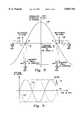
- FIG. 1is an exploded view schematically showing the relative positions of magnetization vectors in the various layers of an anisotropic MR transducer
- FIG. 2is a cross-sectional view schematically illustrating a thin film implementation of the anisotropic MR transducer as shown in FIG. 1;
- FIG. 3is a graphical representation of the normalized resistivity of the active layer in each transducer portion of the anisotropic MR transducer as shown in FIG. 1;
- FIG. 4is waveform diagram displaying the electrical signal in assertive and complementary versions generated from the anisotropic MR transducer as shown in FIG. 1;
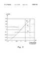
- FIG. 5is a graphical representation showing the substantially linear relationship between direction of the output signal and the flux intercepted by the transducer shown in FIG. 1;
- FIG. 6is an exploded view schematically showing the relative positions of magnetization vectors in the various layers of a giant MR transducer
- FIG. 7is a cross-sectional view schematically illustrating a thin film implementation of the giant MR transducer as shown in FIG. 6;
- FIG. 8is a graphical representation of the normalized resistivity of the active layer in each transducer portion of the giant MR transducer as shown in FIG. 6;
- FIG. 9is waveform diagram displaying the electrical signal in assertive and complementary versions generated from the giant MR transducer as shown in FIG. 6;
- FIG. 10is a graphical representation showing the substantially linear relationship between the output signaland the flux sensed by the giant MR transducer as shown in FIG. 6;
- FIG. 11is an isometric view showing another implementation of the bias layer for the transducers of the invention as shown in FIGS. 1 and 6.
- FIG. 1shows a transducer 2 comprising a bias portion 4 disposed between an assertive transducer portion 6 and a complementary transducer portion 8.
- the bias portion 4includes a bias layer 10 which is electrically insulating and is formed of an antiferromagnetic material.
- An example of such a materialis an oxide of nickel and cobalt alloy (NiCo-O x ).
- NiCo-O xnickel and cobalt alloy
- other nonconducting antiferromagnetic materialscan be used as substitutes, such as ferric oxide (Fe 2 O 3 ) and neodymium ferrous oxide (NdFeO 3 ).
- the assertive and complementary transducer portions 6 and 8comprise first and second ferromagnetic layers 12 and 14, respectively.
- Layers 12 and 14are preferably made of a soft magnetic material which is high in permeability and low in coercive force.
- the ferromagnetic layers 12 and 14are formed of Permalloy, a nickel-iron alloy (NiFe).
- NiFenickel-iron alloy
- the transducer 2flies above a storage medium 18 separated by an air gap 20.
- the storage medium 18can be a tape or disk coated with a magnetic material which provides magnetic storage.
- the medium 18is magnetized with a magnetic flux pattern which corresponds to stored information or data.
- the medium 18moves in a direction of the arrow 24, for example.
- the flux of magnetic transition on the record medium 18is sensed by the transducer 2 as changes in magnetic flux which in turn dynamically alter the resistivity of the ferromagnetic layers 12 and 14. Changes in resistivity of layers 12 and 14 correspond to the information read out from the medium 18.
- the resistivity changesare converted into electrical signals.
- FIG. 2is a cross-sectional view showing a thin film implementation of the transducer 2.
- the transducer 2is preferably fabricated on a ceramic substrate 26 which is nonmagnetic and nonconducting. Above the substrate 26 is the first ferromagnetic layer 12 spaced by an insulator layer 29.
- the bias layer 10is sandwiched between the first ferromagnetic layer 12 and the second ferromagnetic layer 14.
- electrical leads 30 and 32formed of conducting material disposed in contact with each end of the second ferromagnetic layer 14.
- Electrical leads 32 and 36are electrically connected to the inputs 70 and 68, respectively, of the differential amplifier 16 (FIG. 1). Electrical leads 30 and 34 are shorted to ground potential in this embodiment.
- each of the layers 10, 12, and 14is deposited to a thickness of approximately 250 ⁇ , 50 ⁇ , and 50 ⁇ , respectively.
- the directions of magnetic moments of adjacent ions in an antiferromagnetic materialare anti-parallel to each other.
- the direction of magnetization on the surface of a layer of antiferromagnetic materialcan be conditionally sustained, resulting in a directional magnetization in the adjacent ferromagnetic material.
- the magnetic moments of the adjacent ions in any magnetic domain of the materialare aligned in a single direction.
- the gross magnetization of the ferromagnetic materialis determined by magnetization of the dominant domains.
- the first ferromagnetic layer 12 of the transducer 2is first laid above the substrate 26 with an initial direction of uniaxial antisotropy 50.
- the second ferromagnetic layer 14, being in intimate contact with second surface 44 of the antiferromagnetic layer 10orients the surface magnetization of layer 10 at the surface 44 to a direction of magnetization 42 also by the process of exchange coupling.
- the surface magnetization vectors 38 and 42can coexist and are oriented angularly relative to each other within the layer 10 due to the inherent characteristic of the antiferromagnetic material of the layer 10 as mentioned above.
- the surface magnetizations 38 and 42reinforce the directions of uniaxial antisotropy 50 and 52 in layers 12 and 14, respectively. The reinforcement process is iterative. Absent any external influences, this configuration is the lowest maintainable energy state.
- the magnetization vectors 38 and 42provide the necessary magnetic biases to the first and second ferromagnetic layers 12 and 14, respectively. For the purpose of illustration as shown in FIG. 1, the directions of surface magnetization 38 and 42 position themselves at 2 ⁇ with respect to each other.
- a bias current source 56injects currents I1 and I2 into the first and second ferromagnetic layers 12 and 14, respectively.
- Currents I1 and I2flowing in the direction along the longitudinal axis 54, generate magnetic fields 58 and 60, respectively, in accordance with Ampere's law.
- Magnetic fields 58 and 60can alter the angle ⁇ by rotating the directions of uniaxial anistrophy 52 and 50, respectively in opposite directions. In selecting the optimal angle ⁇ as the quiescent operating point, fields 58 and 60 generated by the respective currents I2 and I1 need to be taken into consideration.
- FIG. 3is a graphical representation of the normalized resistivity of either the ferromagnetic layer 12 or 14 as a function of angular orientation of the angle ⁇ . If at proper bias current, the direction of uniaxial anisotropy 50 is optimally oriented by positioning itself at an angle ⁇ of 45° with respect to the longitudinal axis 54, the layer 12 will operate at a quiescent operating point Q, which is well within the linear region of the magnetoresistivity curve 62 as shown in FIG. 3.
- resistivity of a ferromagnetic materialvaries as the square of the cosine of the angle between the direction of magnetization and the direction of current flow. If the storage medium 18 moves in the direction 24 as shown in FIG. 1, then the magnetic flux magnetized on the disk surface passes the transducer 2 which in turn experiences changes in magnetic flux. With reference to the assertive transducer portion 2 if the magnetic flux change is sinusoidal, as shown in FIG. 3 and by reference numeral 64, the first MR layer 12 will change in resistivity along the resistivity curve 62. In essence, the angle ⁇ varies due to the magnetic flux change represented by the curve 64. The quiescent point Q is located in the neighborhood of a linear region.
- the resistance of the first MR layer 12also changes sinusoidally, as represented by the curve 66.
- the bias current I2is constant, and the voltage to the assertive input 68 of the differential amplifier 16 changes sinusoidally as shown by the curve 72 in FIG. 4, in conformance with Ohm's law.
- Similar characteristicsapply to the complementary transducer portion 8. That is, the magnetic flux change 64' triggers the resistance change 66' in the second ferromagnetic layer 14, which in turn generates a voltage curve 72' with opposite polarity as shown in FIG. 4 at the complementary input 70.
- the assertive and complementary voltage curves 72 and 72'are superimposed together in the time domain.
- the amplifier 16accepts differential signals, as shown in FIG. 4, and the voltage difference fed to the assertive and complementary inputs 68 and 70, respectively, are practically doubled.
- This mode of signal transmissionis more immune to noise, such as popcorn noise commonly associated with a magnetic transducer. The reason is when such noise occurs, it impinges on both the assertive and complementary portions 6 and 8 simultaneously.
- noise spikes 74 and 74'respectively impinge on the assertive transducer portion 6 and complementary transducer portion 8.
- the differential voltage received by the amplifier 16remains the same as if the noise event were not existent.
- the transducer 2is highly sensitive to weak signals but capable of screening out undesirable noise. Transducers thus built can interact with storage media having narrow data tracks which emanate weaker magnetic flux, and in noisy environments.
- output signals generated by the transducer 2are relatively symmetrical, due to the inherent symmetrical design of the transducer 2.
- the magnetic biasoriginates directly from the center bias layer 10.
- the two MR layers 12 and 14have no direct influence on each other.
- the output signalsare substantially symmetrical.
- Shown in FIG. 5are the combined output of the two portions 6 and 8 represented by the curve 78.
- the y-axisis the square of the cosine of the magnetization angle ⁇
- the x-axisis the flux emanating from the storage medium measured in milli-electromagnetic units (MEMU), such as Oersteds per square centimeter, for example.
- MEMUmilli-electromagnetic units
- the curve 76is the response of the assertive portion operating alone with the complementary portion 8.
- the curve 76'is the response of the complementary portion operating alone with the assertive portion 6.
- the symmetrical result of the combined output 78is clearly evident from FIG. 5 in comparison with the other outputs.
- transducer 2In most prior art MR transducers, longitudinal bias and transverse magnetic bias are separately and independently provided for the active read layer.
- the longitudinal biasis used to align the active read layer into a single domain state to eliminate Barkhausen noise and the transverse bias is used to orient the active read layer into the active linear region.
- the bias layer 10not only does the bias layer 10 provide both the longitudinal and transverse magnetic biases to the assertive read layer 12, but it also supplies the same types of biases to the complementary bias layer 14. As a consequence, transducer 2 is much less complex in structure and more economical to fabricate.
- the above described transduceris called an anisotropic MR (AMR) transducer.
- AMRanisotropic MR
- GMRgiant MR
- FIG. 6shows schematically the second embodiment of the invention of a transducer 102, which comprises an exchange pinning layer portion 4 disposed between two spin valve portions 106 and 108.
- the exchange pinning portion 4includes a bias layer 10 formed of a material which is electrically insulating and antiferromagnetic. Suitable materials for the bias layer 10 include nickel cobalt alloy oxide (NiCo-O x ), ferric oxide (Fe 2 O 3 ) or nickel oxide (NiO).
- the spin valve 106comprises a pinned layer 106A, a spacer layer 106B and a free layer 106C.
- the spacer layer 106Bis disposed between the pinned layer 106A and the free layer 106C.
- the pinned layer 106A and the free layer 106Care preferably made of softer ferromagnetic materials having a high permeability and a low coercive force.
- the spacer layer 106Bis formed of a nonmagnetic and conducting material such as copper (Cu), gold (Au) or silver (Ag).
- the thickness of the spacer layers 106B and 108Bis significant in the design of the transducer 102.
- the thickness of the spacer layer 106Bshould be thick enough to minimize the exchange coupling between the pinned layer 106A and the active layer 106C, and yet thin enough to enhance spin valve effect. That is, the thickness of the spacer layer 106B needs to be smaller than the mean free path of the conduction electrons from the pinned layer 106A to pass into the active layer 106C.
- the same restrictionsapply to the thickness of the spacer layer 108B in the complementary transducer portion 108.
- the complementary transducer portion 108includes a spacer layer 108B disposed between a pinned layer 108A and active layer 108C.
- the complementary transducer portion 108is a mirror image of the assertive transducer portion 106 about the exchange coupling portion 4 in this embodiment. For the sake of conciseness, a detailed structural description of the complementary transducer portion 108 is not provided.
- the magnetoresistivity of the transducer 102is highly sensitive to external magnetic flux changes. It has been found that the magnetoresistivity varies as a function of the cosine of the angle between the directions of magnetization of the pinned layer and the active layer. In this embodiment, the transducer 102 is operated under the GMR effect, or alternatively the spin valve effect.
- FIG. 7is a sketch of a cross-sectional view showing a thin film implementation of the transducer 102.
- the transducer 102is preferably fabricated on a nonmagnetic and nonconducting substrate 26, such as ceramic.
- a nonmagnetic and nonconducting substrate 26such as ceramic.
- the assertive transducer portion 106which includes the active layer 106C, the spacer layer 106B and the pinned layer 106A.
- the exchange coupling layer 10is laid above the pinned layer 106A.
- the complementary transducer portion 108is built on the top of the bias layer 10.
- the complementary portion 108includes the active layer 108C, the spacer layer 108B and the pinned layer 108A.
- electrical leads 30 and 32there are two conducting leads, namely, electrical lead 30 and 32, disposed in contact with each end of the active layer 108C.
- electrical leads 34 and 36formed of conducting material disposed in contact with each end of the other active layer 106C.
- Electrical leads 32 and 36are electrically connected to the differential amplifier 16 (FIG. 6). Electrical leads 30.and 34 are grounded in this embodiment.
- the thickness of the layers 108C, 108B, 108A, 10, 106A, 106B, and 106Care respectively 20-100 ⁇ , 10-50 ⁇ , 10-100 ⁇ , 50-500 ⁇ , 10-100 ⁇ , 10-50 ⁇ , and 20-100 ⁇ .
- FIG. 6shows the directions of magnetization between the various layers.
- the pinned layers 106A and 108Aare fabricated with initial directions of uniaxial anistropy 118 and 120, respectively. However, pinned layers 106A and 108A are in intimate contact with the surfaces 114 and 116, respectively, of the bias layer 10. As explained before, surface magnetizations 110 and 112 are sustained on each of the major surfaces 114 and 116, respectively, of the bias layer 10. In return, in the layer 106A, a direction of magnetization 118 is pinned parallel to the vector 110 in the layer 10 through the process of exchange coupling. Similarly, in the layer 108A, another direction of magnetization 120 is pinned parallel to the vector 112 in the layer 10. As mentioned before, the pinned layers 106A and 108A are made of ferromagnetic materials with a relatively high coercive force to withstand external field changes without much perturbation.
- the following descriptionis directed to the pinned portion 106. Operation of the complementary transducer portion 108 is substantially similar with minor modifications.
- the free layer 106Cis disposed parallel to and spaced from the pinned layer 106A through the spacer layer 106B.
- the free layer 106Cis initially fabricated with a direction of uniaxial anisotropy, signified by the reference numeral 122A, perpendicular with respect to the traversing axis 55.
- the resistivity of the spin valve layers 106 and 108varies as the cosine of the angle ⁇ and - ⁇ between the directions of magnetization of the pinned layers 106A and 106B and free layers 106C and 108C respectively.
- the transducer 102When the transducer 102 is positioned above the storage medium 18, magnetic flux changes emanating from the medium 18 rotates the magnetization directions 122 and 124 and accordingly, the angle ⁇ varies.
- FIG. 8is a graphical representation of the normalized resistivity of either the active layers 106C or 108C as a function of the angular orientation of the angle ⁇ .
- the active layer 106Coperates at a quiescent operating point Q, which is well within the linear region of the magnetoresistivity curve 126 as shown in FIG. 8.
- the operating point of the active layer 108Cis placed at the quiescent point -Q in the magnetoresistivity curve 126 shown in FIG. 8.
- the magnetic flux magnetized on the disk surfacepasses the transducer 102 which in turn experiences changes in magnetic flux.
- the magnetic flux changeis sinusoidal, as shown in FIG. 8 by the graphical representation signified by the reference numeral 64, then in response, the spin valve 106 changes in resistivity along magnetoresistivity curve 126.
- the angle avaries due to the magnetic flux change represented by the curve 126.
- the quiescent point Qis located in the neighborhood of a linear region, the resistance of the spin valve 106 also changes sinusoidally, as represented by the curve 128.
- the current I1is constant, the voltage to the input 68 of the differential amplifier 16 also changes sinusoidally as shown by the curve 132 in FIG.
- the voltage curves 132 and 132'are superimposed together in the same time domain.
- the amplifier 16accepts differential signals as can been seen in FIG. 9, and the voltage difference fed to the inputs 68 and 70, respectively, are practically doubled. As explained before, this mode of signal transmission is more immune to noise, such as popcorn noise commonly associated with a magnetic transducer.
- a noise spike 74 on the transducer 102is equally received by the spin valve 106 and the spin valve 108.
- the differential voltage received by the amplifier 16remains the same as if the noise event were nonexistent.
- the transducer 102is therefore capable of screening out undesirable noise yet maintains its high sensitivity to weak signals.
- the transducer 102 as fabricatedcan interact with storage media having narrow data tracks which emanate weaker magnetic flux, and in noisy environments.
- signals generated by the transducer 102is relatively symmetrical, due to the inherent symmetrical design of the transducer 102.
- Shown in FIG. 10are the combined output of the two spin valves 106 and 108 represented by the curve 136.
- the y-axisis the cosine of the magnetization angle ⁇ , and the x-axis is the flux emanating from the storage medium.
- Bias portion 4'is a composite layer including an insulating sublayer 4A sandwiched between two electrically conducting sublayers 4B and 4C. Deposited in contact with each of the layers 4B and 4C are antiferromagnetic sublayers 4E and 4F, respectively.
- the insulating sublayer 4Acan be made of an electrically insulating and nonmagnetic material, such as alumina (Al 2 O 3 ).
- Conducting sublayers 4B and 4Care made from electrically conducting but nonmagnetic materials.
- sublayers 4B and 4Cexamples are copper, gold and silver.
- the sublayers 4E and 4Fcan be built of antiferromagnetic material such as ferrous manganese (FeMn).
- FeMnferrous manganese
- directions of magnetization on the surfaces of the bias portion 4'can be oriented in any desired directions during fabrication, as disclosed in the referenced copending application.
Landscapes
- Engineering & Computer Science (AREA)
- Physics & Mathematics (AREA)
- Nanotechnology (AREA)
- Chemical & Material Sciences (AREA)
- General Physics & Mathematics (AREA)
- Crystallography & Structural Chemistry (AREA)
- Condensed Matter Physics & Semiconductors (AREA)
- Mathematical Physics (AREA)
- Theoretical Computer Science (AREA)
- Manufacturing & Machinery (AREA)
- Hall/Mr Elements (AREA)
- Measuring Magnetic Variables (AREA)
- Magnetic Heads (AREA)
Abstract
Description
Claims (9)
Priority Applications (3)
| Application Number | Priority Date | Filing Date | Title |
|---|---|---|---|
| US08/833,058US5859754A (en) | 1997-04-03 | 1997-04-03 | Magnetoresistive transducer having a common magnetic bias using assertive and complementary signals |
| JP10108739AJPH10283615A (en) | 1997-04-03 | 1998-04-03 | Magneto-resistive type converter |
| US09/651,053US6392850B1 (en) | 1997-04-03 | 1998-10-19 | Magnetoresistive transducer having a common magnetic bias using assertive and complementary signals |
Applications Claiming Priority (1)
| Application Number | Priority Date | Filing Date | Title |
|---|---|---|---|
| US08/833,058US5859754A (en) | 1997-04-03 | 1997-04-03 | Magnetoresistive transducer having a common magnetic bias using assertive and complementary signals |
Related Child Applications (1)
| Application Number | Title | Priority Date | Filing Date |
|---|---|---|---|
| US09/651,053DivisionUS6392850B1 (en) | 1997-04-03 | 1998-10-19 | Magnetoresistive transducer having a common magnetic bias using assertive and complementary signals |
Publications (1)
| Publication Number | Publication Date |
|---|---|
| US5859754Atrue US5859754A (en) | 1999-01-12 |
Family
ID=25263307
Family Applications (2)
| Application Number | Title | Priority Date | Filing Date |
|---|---|---|---|
| US08/833,058Expired - LifetimeUS5859754A (en) | 1997-04-03 | 1997-04-03 | Magnetoresistive transducer having a common magnetic bias using assertive and complementary signals |
| US09/651,053Expired - Fee RelatedUS6392850B1 (en) | 1997-04-03 | 1998-10-19 | Magnetoresistive transducer having a common magnetic bias using assertive and complementary signals |
Family Applications After (1)
| Application Number | Title | Priority Date | Filing Date |
|---|---|---|---|
| US09/651,053Expired - Fee RelatedUS6392850B1 (en) | 1997-04-03 | 1998-10-19 | Magnetoresistive transducer having a common magnetic bias using assertive and complementary signals |
Country Status (2)
| Country | Link |
|---|---|
| US (2) | US5859754A (en) |
| JP (1) | JPH10283615A (en) |
Cited By (26)
| Publication number | Priority date | Publication date | Assignee | Title |
|---|---|---|---|---|
| WO2000045190A1 (en)* | 1999-01-28 | 2000-08-03 | Robert Bosch Gmbh | Device and method for determining a magnetic field |
| US6178073B1 (en)* | 1997-12-01 | 2001-01-23 | Nec Corporation | Magneto-resistance effect element with a fixing layer formed from a superlattice of at least two different materials and production method of the same |
| US6185079B1 (en)* | 1998-11-09 | 2001-02-06 | International Business Machines Corporation | Disk drive with thermal asperity reduction circuitry using a magnetic tunnel junction sensor |
| US6252796B1 (en)* | 1998-08-14 | 2001-06-26 | U.S. Philips Corporation | Device comprising a first and a second ferromagnetic layer separated by a non-magnetic spacer layer |
| US6278594B1 (en)* | 1998-10-13 | 2001-08-21 | Storage Technology Corporation | Dual element magnetoresistive read head with integral element stabilization |
| US6278589B1 (en)* | 1999-03-30 | 2001-08-21 | International Business Machines Corporation | Dual GMR sensor with a single AFM layer |
| US6366420B1 (en) | 1999-07-13 | 2002-04-02 | Texas Instruments Incorporated | Method of restoring the orientation of a pinned layer of a magnetoresistive head |
| US6452204B1 (en)* | 1998-12-08 | 2002-09-17 | Nec Corporation | Tunneling magnetoresistance transducer and method for manufacturing the same |
| US20030002231A1 (en)* | 2001-06-29 | 2003-01-02 | Dee Richard Henry | Reduced sensitivity spin valve head for magnetic tape applications |
| US20030002232A1 (en)* | 2001-06-29 | 2003-01-02 | Storage Technology Corporation | Apparatus and method of making a reduced sensitivity spin valve sensor apparatus in which a flux carrying capacity is increased |
| WO2003003355A1 (en)* | 2001-06-29 | 2003-01-09 | Storage Technology Corporation | Apparatus and method of making a reduced sensitivity spin valve sensor apparatus in which a basic magnetic sensitivity is reduced |
| US6532823B1 (en)* | 1999-03-18 | 2003-03-18 | Read-Rite Corporation | Insulator layers for magnetoresistive transducers |
| US6556388B1 (en)* | 1998-11-20 | 2003-04-29 | Seagate Technology Llc | Differential VGMR sensor |
| US6594124B2 (en) | 2001-11-06 | 2003-07-15 | Headway Technologies, Inc. | Canted adjacent layer stabilized SV heads |
| US20030184918A1 (en)* | 2002-04-02 | 2003-10-02 | International Business Machines Corporation | Dual spin valve sensor with a longitudinal bias stack |
| US20030184919A1 (en)* | 2002-04-02 | 2003-10-02 | International Business Machines Corporation | Dual magnetic tunnel junction sensor with a longitudinal bias stack |
| US6631057B1 (en)* | 1999-03-19 | 2003-10-07 | International Business Machines Corporation | Magnetic device with ferromagnetic layer contacting specified yttrium or rare earth element oxide antiferromagnetic layer |
| US6667861B2 (en) | 2001-07-16 | 2003-12-23 | International Business Machines Corporation | Dual/differential GMR head with a single AFM layer |
| US20040007751A1 (en)* | 2002-07-15 | 2004-01-15 | John Mattson | Magnetoresistive memory devices |
| US6754048B2 (en)* | 1999-08-16 | 2004-06-22 | Headway Technologies, Inc. | Multiple magnetoresistive (MR) layer sensor element having longitudinal bias layers with non-parallel magnetizations |
| US20050079132A1 (en)* | 2003-04-08 | 2005-04-14 | Xingwu Wang | Medical device with low magnetic susceptibility |
| US20050128653A1 (en)* | 2003-12-12 | 2005-06-16 | Gill Hardayal S. | Top CPP GMR/TV with back end of stripe pinned by insulating AFM |
| US20050180062A1 (en)* | 2004-02-18 | 2005-08-18 | Ho Kuok S. | GMR sensor with oriented hard bias stabilization |
| US20070010702A1 (en)* | 2003-04-08 | 2007-01-11 | Xingwu Wang | Medical device with low magnetic susceptibility |
| US7382585B1 (en)* | 2005-09-30 | 2008-06-03 | Storage Technology Corporation | Magnetic head having AMR reader, writer, and GMR reader |
| DE10014780B4 (en)* | 2000-03-27 | 2009-07-30 | Philips Intellectual Property & Standards Gmbh | MR angle sensor |
Families Citing this family (134)
| Publication number | Priority date | Publication date | Assignee | Title |
|---|---|---|---|---|
| JP4182728B2 (en)* | 2002-11-15 | 2008-11-19 | ソニー株式会社 | Magnetic storage element recording method and magnetic storage device |
| JP2007323725A (en)* | 2006-05-31 | 2007-12-13 | Toshiba Corp | Vertically energized magnetic head and magnetic disk device using the same |
| US8689430B1 (en) | 2006-11-29 | 2014-04-08 | Western Digital (Fremont), Llc | Method for providing a perpendicular magnetic recording (PMR)head |
| US8404128B1 (en) | 2009-02-23 | 2013-03-26 | Western Digital (Fremont), Llc | Method and system for providing a perpendicular magnetic recording head |
| US8400731B1 (en) | 2009-04-19 | 2013-03-19 | Western Digital (Fremont), Llc | Write head with variable side shield gaps |
| US8611055B1 (en) | 2009-07-31 | 2013-12-17 | Western Digital (Fremont), Llc | Magnetic etch-stop layer for magnetoresistive read heads |
| US9202480B2 (en) | 2009-10-14 | 2015-12-01 | Western Digital (Fremont), LLC. | Double patterning hard mask for damascene perpendicular magnetic recording (PMR) writer |
| US8441896B2 (en) | 2010-06-25 | 2013-05-14 | Western Digital (Fremont), Llc | Energy assisted magnetic recording head having laser integrated mounted to slider |
| US8997832B1 (en) | 2010-11-23 | 2015-04-07 | Western Digital (Fremont), Llc | Method of fabricating micrometer scale components |
| US8441756B1 (en) | 2010-12-16 | 2013-05-14 | Western Digital (Fremont), Llc | Method and system for providing an antiferromagnetically coupled writer |
| US9123359B1 (en) | 2010-12-22 | 2015-09-01 | Western Digital (Fremont), Llc | Magnetic recording transducer with sputtered antiferromagnetic coupling trilayer between plated ferromagnetic shields and method of fabrication |
| US8456961B1 (en) | 2011-03-22 | 2013-06-04 | Western Digital (Fremont), Llc | Systems and methods for mounting and aligning a laser in an electrically assisted magnetic recording assembly |
| US8419954B1 (en) | 2011-10-31 | 2013-04-16 | Western Digital (Fremont), Llc | Method for providing a side shield for a magnetic recording transducer |
| US8760823B1 (en) | 2011-12-20 | 2014-06-24 | Western Digital (Fremont), Llc | Method and system for providing a read transducer having soft and hard magnetic bias structures |
| US8451563B1 (en) | 2011-12-20 | 2013-05-28 | Western Digital (Fremont), Llc | Method for providing a side shield for a magnetic recording transducer using an air bridge |
| US9093639B2 (en) | 2012-02-21 | 2015-07-28 | Western Digital (Fremont), Llc | Methods for manufacturing a magnetoresistive structure utilizing heating and cooling |
| US9349392B1 (en) | 2012-05-24 | 2016-05-24 | Western Digital (Fremont), Llc | Methods for improving adhesion on dielectric substrates |
| US8724259B1 (en) | 2012-06-11 | 2014-05-13 | Western Digital (Fremont), Llc | Conformal high moment side shield seed layer for perpendicular magnetic recording writer |
| US8711528B1 (en) | 2012-06-29 | 2014-04-29 | Western Digital (Fremont), Llc | Tunnel magnetoresistance read head with narrow shield-to-shield spacing |
| US9269382B1 (en) | 2012-06-29 | 2016-02-23 | Western Digital (Fremont), Llc | Method and system for providing a read transducer having improved pinning of the pinned layer at higher recording densities |
| US9213322B1 (en) | 2012-08-16 | 2015-12-15 | Western Digital (Fremont), Llc | Methods for providing run to run process control using a dynamic tuner |
| US8984740B1 (en) | 2012-11-30 | 2015-03-24 | Western Digital (Fremont), Llc | Process for providing a magnetic recording transducer having a smooth magnetic seed layer |
| US9053719B2 (en) | 2012-11-30 | 2015-06-09 | Western Digital (Fremont), Llc | Magnetoresistive sensor for a magnetic storage system read head, and fabrication method thereof |
| US8980109B1 (en) | 2012-12-11 | 2015-03-17 | Western Digital (Fremont), Llc | Method for providing a magnetic recording transducer using a combined main pole and side shield CMP for a wraparound shield scheme |
| US8760818B1 (en) | 2013-01-09 | 2014-06-24 | Western Digital (Fremont), Llc | Systems and methods for providing magnetic storage elements with high magneto-resistance using heusler alloys |
| US9042208B1 (en) | 2013-03-11 | 2015-05-26 | Western Digital Technologies, Inc. | Disk drive measuring fly height by applying a bias voltage to an electrically insulated write component of a head |
| US8883017B1 (en) | 2013-03-12 | 2014-11-11 | Western Digital (Fremont), Llc | Method and system for providing a read transducer having seamless interfaces |
| US9336814B1 (en) | 2013-03-12 | 2016-05-10 | Western Digital (Fremont), Llc | Inverse tapered waveguide for use in a heat assisted magnetic recording head |
| US9111564B1 (en) | 2013-04-02 | 2015-08-18 | Western Digital (Fremont), Llc | Magnetic recording writer having a main pole with multiple flare angles |
| US9013836B1 (en) | 2013-04-02 | 2015-04-21 | Western Digital (Fremont), Llc | Method and system for providing an antiferromagnetically coupled return pole |
| US9104107B1 (en) | 2013-04-03 | 2015-08-11 | Western Digital (Fremont), Llc | DUV photoresist process |
| US8993217B1 (en) | 2013-04-04 | 2015-03-31 | Western Digital (Fremont), Llc | Double exposure technique for high resolution disk imaging |
| US9064527B1 (en) | 2013-04-12 | 2015-06-23 | Western Digital (Fremont), Llc | High order tapered waveguide for use in a heat assisted magnetic recording head |
| US9245545B1 (en) | 2013-04-12 | 2016-01-26 | Wester Digital (Fremont), Llc | Short yoke length coils for magnetic heads in disk drives |
| US9070381B1 (en) | 2013-04-12 | 2015-06-30 | Western Digital (Fremont), Llc | Magnetic recording read transducer having a laminated free layer |
| US9431047B1 (en) | 2013-05-01 | 2016-08-30 | Western Digital (Fremont), Llc | Method for providing an improved AFM reader shield |
| US9064528B1 (en) | 2013-05-17 | 2015-06-23 | Western Digital Technologies, Inc. | Interferometric waveguide usable in shingled heat assisted magnetic recording in the absence of a near-field transducer |
| US9431039B1 (en) | 2013-05-21 | 2016-08-30 | Western Digital (Fremont), Llc | Multiple sensor array usable in two-dimensional magnetic recording |
| US9263067B1 (en) | 2013-05-29 | 2016-02-16 | Western Digital (Fremont), Llc | Process for making PMR writer with constant side wall angle |
| US9361913B1 (en) | 2013-06-03 | 2016-06-07 | Western Digital (Fremont), Llc | Recording read heads with a multi-layer AFM layer methods and apparatuses |
| US9406331B1 (en) | 2013-06-17 | 2016-08-02 | Western Digital (Fremont), Llc | Method for making ultra-narrow read sensor and read transducer device resulting therefrom |
| US9287494B1 (en) | 2013-06-28 | 2016-03-15 | Western Digital (Fremont), Llc | Magnetic tunnel junction (MTJ) with a magnesium oxide tunnel barrier |
| US9318130B1 (en) | 2013-07-02 | 2016-04-19 | Western Digital (Fremont), Llc | Method to fabricate tunneling magnetic recording heads with extended pinned layer |
| US8947985B1 (en) | 2013-07-16 | 2015-02-03 | Western Digital (Fremont), Llc | Heat assisted magnetic recording transducers having a recessed pole |
| US8923102B1 (en) | 2013-07-16 | 2014-12-30 | Western Digital (Fremont), Llc | Optical grating coupling for interferometric waveguides in heat assisted magnetic recording heads |
| US9431032B1 (en) | 2013-08-14 | 2016-08-30 | Western Digital (Fremont), Llc | Electrical connection arrangement for a multiple sensor array usable in two-dimensional magnetic recording |
| US9275657B1 (en) | 2013-08-14 | 2016-03-01 | Western Digital (Fremont), Llc | Process for making PMR writer with non-conformal side gaps |
| US9042051B2 (en) | 2013-08-15 | 2015-05-26 | Western Digital (Fremont), Llc | Gradient write gap for perpendicular magnetic recording writer |
| US9343098B1 (en) | 2013-08-23 | 2016-05-17 | Western Digital (Fremont), Llc | Method for providing a heat assisted magnetic recording transducer having protective pads |
| US9343086B1 (en) | 2013-09-11 | 2016-05-17 | Western Digital (Fremont), Llc | Magnetic recording write transducer having an improved sidewall angle profile |
| US9441938B1 (en) | 2013-10-08 | 2016-09-13 | Western Digital (Fremont), Llc | Test structures for measuring near field transducer disc length |
| US9042058B1 (en) | 2013-10-17 | 2015-05-26 | Western Digital Technologies, Inc. | Shield designed for middle shields in a multiple sensor array |
| US9349394B1 (en) | 2013-10-18 | 2016-05-24 | Western Digital (Fremont), Llc | Method for fabricating a magnetic writer having a gradient side gap |
| US9007719B1 (en) | 2013-10-23 | 2015-04-14 | Western Digital (Fremont), Llc | Systems and methods for using double mask techniques to achieve very small features |
| US9214172B2 (en) | 2013-10-23 | 2015-12-15 | Western Digital (Fremont), Llc | Method of manufacturing a magnetic read head |
| US8988812B1 (en) | 2013-11-27 | 2015-03-24 | Western Digital (Fremont), Llc | Multi-sensor array configuration for a two-dimensional magnetic recording (TDMR) operation |
| US9349391B2 (en)* | 2013-12-04 | 2016-05-24 | HGST Netherlands B.V. | Controlling magnetic layer anisotropy field by oblique angle static deposition |
| US9194692B1 (en) | 2013-12-06 | 2015-11-24 | Western Digital (Fremont), Llc | Systems and methods for using white light interferometry to measure undercut of a bi-layer structure |
| US9280990B1 (en) | 2013-12-11 | 2016-03-08 | Western Digital (Fremont), Llc | Method for fabricating a magnetic writer using multiple etches |
| US9001628B1 (en) | 2013-12-16 | 2015-04-07 | Western Digital (Fremont), Llc | Assistant waveguides for evaluating main waveguide coupling efficiency and diode laser alignment tolerances for hard disk |
| US8917581B1 (en) | 2013-12-18 | 2014-12-23 | Western Digital Technologies, Inc. | Self-anneal process for a near field transducer and chimney in a hard disk drive assembly |
| US9082423B1 (en) | 2013-12-18 | 2015-07-14 | Western Digital (Fremont), Llc | Magnetic recording write transducer having an improved trailing surface profile |
| US8971160B1 (en) | 2013-12-19 | 2015-03-03 | Western Digital (Fremont), Llc | Near field transducer with high refractive index pin for heat assisted magnetic recording |
| US9147408B1 (en) | 2013-12-19 | 2015-09-29 | Western Digital (Fremont), Llc | Heated AFM layer deposition and cooling process for TMR magnetic recording sensor with high pinning field |
| US8970988B1 (en) | 2013-12-31 | 2015-03-03 | Western Digital (Fremont), Llc | Electric gaps and method for making electric gaps for multiple sensor arrays |
| US9305583B1 (en) | 2014-02-18 | 2016-04-05 | Western Digital (Fremont), Llc | Method for fabricating a magnetic writer using multiple etches of damascene materials |
| US9183854B2 (en) | 2014-02-24 | 2015-11-10 | Western Digital (Fremont), Llc | Method to make interferometric taper waveguide for HAMR light delivery |
| US9202493B1 (en) | 2014-02-28 | 2015-12-01 | Western Digital (Fremont), Llc | Method of making an ultra-sharp tip mode converter for a HAMR head |
| US9396743B1 (en) | 2014-02-28 | 2016-07-19 | Western Digital (Fremont), Llc | Systems and methods for controlling soft bias thickness for tunnel magnetoresistance readers |
| US8988825B1 (en) | 2014-02-28 | 2015-03-24 | Western Digital (Fremont, LLC | Method for fabricating a magnetic writer having half-side shields |
| US9142233B1 (en) | 2014-02-28 | 2015-09-22 | Western Digital (Fremont), Llc | Heat assisted magnetic recording writer having a recessed pole |
| US9153255B1 (en) | 2014-03-05 | 2015-10-06 | Western Digital (Fremont), Llc | Method for fabricating a magnetic writer having an asymmetric gap and shields |
| US9001467B1 (en) | 2014-03-05 | 2015-04-07 | Western Digital (Fremont), Llc | Method for fabricating side shields in a magnetic writer |
| US9135930B1 (en) | 2014-03-06 | 2015-09-15 | Western Digital (Fremont), Llc | Method for fabricating a magnetic write pole using vacuum deposition |
| US9934811B1 (en) | 2014-03-07 | 2018-04-03 | Western Digital (Fremont), Llc | Methods for controlling stray fields of magnetic features using magneto-elastic anisotropy |
| US9190085B1 (en) | 2014-03-12 | 2015-11-17 | Western Digital (Fremont), Llc | Waveguide with reflective grating for localized energy intensity |
| US9111558B1 (en) | 2014-03-14 | 2015-08-18 | Western Digital (Fremont), Llc | System and method of diffractive focusing of light in a waveguide |
| US9135937B1 (en) | 2014-05-09 | 2015-09-15 | Western Digital (Fremont), Llc | Current modulation on laser diode for energy assisted magnetic recording transducer |
| US9007879B1 (en) | 2014-06-10 | 2015-04-14 | Western Digital (Fremont), Llc | Interfering near field transducer having a wide metal bar feature for energy assisted magnetic recording |
| US8976635B1 (en) | 2014-06-10 | 2015-03-10 | Western Digital (Fremont), Llc | Near field transducer driven by a transverse electric waveguide for energy assisted magnetic recording |
| US8958272B1 (en) | 2014-06-10 | 2015-02-17 | Western Digital (Fremont), Llc | Interfering near field transducer for energy assisted magnetic recording |
| US8953422B1 (en) | 2014-06-10 | 2015-02-10 | Western Digital (Fremont), Llc | Near field transducer using dielectric waveguide core with fine ridge feature |
| US9508363B1 (en) | 2014-06-17 | 2016-11-29 | Western Digital (Fremont), Llc | Method for fabricating a magnetic write pole having a leading edge bevel |
| US9361914B1 (en) | 2014-06-18 | 2016-06-07 | Western Digital (Fremont), Llc | Magnetic sensor with thin capping layer |
| US9053735B1 (en) | 2014-06-20 | 2015-06-09 | Western Digital (Fremont), Llc | Method for fabricating a magnetic writer using a full-film metal planarization |
| US9214169B1 (en) | 2014-06-20 | 2015-12-15 | Western Digital (Fremont), Llc | Magnetic recording read transducer having a laminated free layer |
| US9042052B1 (en) | 2014-06-23 | 2015-05-26 | Western Digital (Fremont), Llc | Magnetic writer having a partially shunted coil |
| US9230565B1 (en) | 2014-06-24 | 2016-01-05 | Western Digital (Fremont), Llc | Magnetic shield for magnetic recording head |
| US9190079B1 (en) | 2014-09-22 | 2015-11-17 | Western Digital (Fremont), Llc | Magnetic write pole having engineered radius of curvature and chisel angle profiles |
| US9007725B1 (en) | 2014-10-07 | 2015-04-14 | Western Digital (Fremont), Llc | Sensor with positive coupling between dual ferromagnetic free layer laminates |
| US9087527B1 (en) | 2014-10-28 | 2015-07-21 | Western Digital (Fremont), Llc | Apparatus and method for middle shield connection in magnetic recording transducers |
| US9786301B1 (en) | 2014-12-02 | 2017-10-10 | Western Digital (Fremont), Llc | Apparatuses and methods for providing thin shields in a multiple sensor array |
| US9111550B1 (en) | 2014-12-04 | 2015-08-18 | Western Digital (Fremont), Llc | Write transducer having a magnetic buffer layer spaced between a side shield and a write pole by non-magnetic layers |
| US9721595B1 (en) | 2014-12-04 | 2017-08-01 | Western Digital (Fremont), Llc | Method for providing a storage device |
| US9236560B1 (en) | 2014-12-08 | 2016-01-12 | Western Digital (Fremont), Llc | Spin transfer torque tunneling magnetoresistive device having a laminated free layer with perpendicular magnetic anisotropy |
| US9286919B1 (en) | 2014-12-17 | 2016-03-15 | Western Digital (Fremont), Llc | Magnetic writer having a dual side gap |
| US9881638B1 (en) | 2014-12-17 | 2018-01-30 | Western Digital (Fremont), Llc | Method for providing a near-field transducer (NFT) for a heat assisted magnetic recording (HAMR) device |
| US9214165B1 (en) | 2014-12-18 | 2015-12-15 | Western Digital (Fremont), Llc | Magnetic writer having a gradient in saturation magnetization of the shields |
| US9741366B1 (en) | 2014-12-18 | 2017-08-22 | Western Digital (Fremont), Llc | Method for fabricating a magnetic writer having a gradient in saturation magnetization of the shields |
| US9343087B1 (en) | 2014-12-21 | 2016-05-17 | Western Digital (Fremont), Llc | Method for fabricating a magnetic writer having half shields |
| US10074387B1 (en) | 2014-12-21 | 2018-09-11 | Western Digital (Fremont), Llc | Method and system for providing a read transducer having symmetric antiferromagnetically coupled shields |
| US9437251B1 (en) | 2014-12-22 | 2016-09-06 | Western Digital (Fremont), Llc | Apparatus and method having TDMR reader to reader shunts |
| US9449625B1 (en) | 2014-12-24 | 2016-09-20 | Western Digital (Fremont), Llc | Heat assisted magnetic recording head having a plurality of diffusion barrier layers |
| US9123374B1 (en) | 2015-02-12 | 2015-09-01 | Western Digital (Fremont), Llc | Heat assisted magnetic recording writer having an integrated polarization rotation plate |
| US9312064B1 (en) | 2015-03-02 | 2016-04-12 | Western Digital (Fremont), Llc | Method to fabricate a magnetic head including ion milling of read gap using dual layer hard mask |
| US9443541B1 (en) | 2015-03-24 | 2016-09-13 | Western Digital (Fremont), Llc | Magnetic writer having a gradient in saturation magnetization of the shields and return pole |
| US9431031B1 (en) | 2015-03-24 | 2016-08-30 | Western Digital (Fremont), Llc | System and method for magnetic transducers having multiple sensors and AFC shields |
| US9384763B1 (en) | 2015-03-26 | 2016-07-05 | Western Digital (Fremont), Llc | Dual free layer magnetic reader having a rear bias structure including a soft bias layer |
| US9449621B1 (en) | 2015-03-26 | 2016-09-20 | Western Digital (Fremont), Llc | Dual free layer magnetic reader having a rear bias structure having a high aspect ratio |
| US9245562B1 (en) | 2015-03-30 | 2016-01-26 | Western Digital (Fremont), Llc | Magnetic recording writer with a composite main pole |
| US9147404B1 (en) | 2015-03-31 | 2015-09-29 | Western Digital (Fremont), Llc | Method and system for providing a read transducer having a dual free layer |
| US9263071B1 (en) | 2015-03-31 | 2016-02-16 | Western Digital (Fremont), Llc | Flat NFT for heat assisted magnetic recording |
| US9508372B1 (en) | 2015-06-03 | 2016-11-29 | Western Digital (Fremont), Llc | Shingle magnetic writer having a low sidewall angle pole |
| US9508365B1 (en) | 2015-06-24 | 2016-11-29 | Western Digital (Fremont), LLC. | Magnetic reader having a crystal decoupling structure |
| US9530443B1 (en) | 2015-06-25 | 2016-12-27 | Western Digital (Fremont), Llc | Method for fabricating a magnetic recording device having a high aspect ratio structure |
| US9842615B1 (en) | 2015-06-26 | 2017-12-12 | Western Digital (Fremont), Llc | Magnetic reader having a nonmagnetic insertion layer for the pinning layer |
| US9646639B2 (en) | 2015-06-26 | 2017-05-09 | Western Digital (Fremont), Llc | Heat assisted magnetic recording writer having integrated polarization rotation waveguides |
| US9431038B1 (en) | 2015-06-29 | 2016-08-30 | Western Digital (Fremont), Llc | Method for fabricating a magnetic write pole having an improved sidewall angle profile |
| US9666214B1 (en) | 2015-09-23 | 2017-05-30 | Western Digital (Fremont), Llc | Free layer magnetic reader that may have a reduced shield-to-shield spacing |
| US9472216B1 (en) | 2015-09-23 | 2016-10-18 | Western Digital (Fremont), Llc | Differential dual free layer magnetic reader |
| US9384765B1 (en) | 2015-09-24 | 2016-07-05 | Western Digital (Fremont), Llc | Method and system for providing a HAMR writer having improved optical efficiency |
| US9424866B1 (en) | 2015-09-24 | 2016-08-23 | Western Digital (Fremont), Llc | Heat assisted magnetic recording write apparatus having a dielectric gap |
| US9595273B1 (en) | 2015-09-30 | 2017-03-14 | Western Digital (Fremont), Llc | Shingle magnetic writer having nonconformal shields |
| US9484051B1 (en) | 2015-11-09 | 2016-11-01 | The Provost, Fellows, Foundation Scholars and the other members of Board, of the College of the Holy and Undivided Trinity of Queen Elizabeth near Dublin | Method and system for reducing undesirable reflections in a HAMR write apparatus |
| US9953670B1 (en) | 2015-11-10 | 2018-04-24 | Western Digital (Fremont), Llc | Method and system for providing a HAMR writer including a multi-mode interference device |
| US10037770B1 (en) | 2015-11-12 | 2018-07-31 | Western Digital (Fremont), Llc | Method for providing a magnetic recording write apparatus having a seamless pole |
| US9812155B1 (en) | 2015-11-23 | 2017-11-07 | Western Digital (Fremont), Llc | Method and system for fabricating high junction angle read sensors |
| US9564150B1 (en) | 2015-11-24 | 2017-02-07 | Western Digital (Fremont), Llc | Magnetic read apparatus having an improved read sensor isolation circuit |
| US9799351B1 (en) | 2015-11-30 | 2017-10-24 | Western Digital (Fremont), Llc | Short yoke length writer having assist coils |
| US9754611B1 (en) | 2015-11-30 | 2017-09-05 | Western Digital (Fremont), Llc | Magnetic recording write apparatus having a stepped conformal trailing shield |
| US9767831B1 (en) | 2015-12-01 | 2017-09-19 | Western Digital (Fremont), Llc | Magnetic writer having convex trailing surface pole and conformal write gap |
| US9740805B1 (en) | 2015-12-01 | 2017-08-22 | Western Digital (Fremont), Llc | Method and system for detecting hotspots for photolithographically-defined devices |
| US9858951B1 (en) | 2015-12-01 | 2018-01-02 | Western Digital (Fremont), Llc | Method for providing a multilayer AFM layer in a read sensor |
| CN107037381A (en)* | 2015-12-29 | 2017-08-11 | 爱盛科技股份有限公司 | Magnetic field sensing device and sensing method thereof |
Citations (2)
| Publication number | Priority date | Publication date | Assignee | Title |
|---|---|---|---|---|
| US5408377A (en)* | 1993-10-15 | 1995-04-18 | International Business Machines Corporation | Magnetoresistive sensor with improved ferromagnetic sensing layer and magnetic recording system using the sensor |
| US5612098A (en)* | 1996-08-14 | 1997-03-18 | Read-Rite Corporation | Method of forming a thin film magnetic structure having ferromagnetic and antiferromagnetic layers |
Family Cites Families (1)
| Publication number | Priority date | Publication date | Assignee | Title |
|---|---|---|---|---|
| JPH09274710A (en)* | 1996-04-04 | 1997-10-21 | Fujitsu Ltd | Spin valve magnetoresistive head, manufacturing method thereof, and magnetic recording apparatus |
- 1997
- 1997-04-03USUS08/833,058patent/US5859754A/ennot_activeExpired - Lifetime
- 1998
- 1998-04-03JPJP10108739Apatent/JPH10283615A/enactivePending
- 1998-10-19USUS09/651,053patent/US6392850B1/ennot_activeExpired - Fee Related
Patent Citations (2)
| Publication number | Priority date | Publication date | Assignee | Title |
|---|---|---|---|---|
| US5408377A (en)* | 1993-10-15 | 1995-04-18 | International Business Machines Corporation | Magnetoresistive sensor with improved ferromagnetic sensing layer and magnetic recording system using the sensor |
| US5612098A (en)* | 1996-08-14 | 1997-03-18 | Read-Rite Corporation | Method of forming a thin film magnetic structure having ferromagnetic and antiferromagnetic layers |
Cited By (47)
| Publication number | Priority date | Publication date | Assignee | Title |
|---|---|---|---|---|
| US6178073B1 (en)* | 1997-12-01 | 2001-01-23 | Nec Corporation | Magneto-resistance effect element with a fixing layer formed from a superlattice of at least two different materials and production method of the same |
| US6252796B1 (en)* | 1998-08-14 | 2001-06-26 | U.S. Philips Corporation | Device comprising a first and a second ferromagnetic layer separated by a non-magnetic spacer layer |
| US6278594B1 (en)* | 1998-10-13 | 2001-08-21 | Storage Technology Corporation | Dual element magnetoresistive read head with integral element stabilization |
| US6674618B2 (en) | 1998-10-13 | 2004-01-06 | Storage Technology Corporation | Dual element magnetoresistive read head with integral element stabilization |
| US6185079B1 (en)* | 1998-11-09 | 2001-02-06 | International Business Machines Corporation | Disk drive with thermal asperity reduction circuitry using a magnetic tunnel junction sensor |
| US6556388B1 (en)* | 1998-11-20 | 2003-04-29 | Seagate Technology Llc | Differential VGMR sensor |
| US6452204B1 (en)* | 1998-12-08 | 2002-09-17 | Nec Corporation | Tunneling magnetoresistance transducer and method for manufacturing the same |
| US6724184B1 (en) | 1999-01-28 | 2004-04-20 | Robert Bosch Gmbh | Device and method for determining a magnetic field as to its intensity and direction |
| WO2000045190A1 (en)* | 1999-01-28 | 2000-08-03 | Robert Bosch Gmbh | Device and method for determining a magnetic field |
| CZ300974B6 (en)* | 1999-01-28 | 2009-09-30 | Robert Bosch Gmbh | Device for and method of determining magnetic field |
| US6532823B1 (en)* | 1999-03-18 | 2003-03-18 | Read-Rite Corporation | Insulator layers for magnetoresistive transducers |
| EP1039490B1 (en)* | 1999-03-19 | 2006-08-09 | Hitachi Global Storage Technologies Netherlands B.V. | Pinning layer for magnetic devices |
| US6631057B1 (en)* | 1999-03-19 | 2003-10-07 | International Business Machines Corporation | Magnetic device with ferromagnetic layer contacting specified yttrium or rare earth element oxide antiferromagnetic layer |
| US6278589B1 (en)* | 1999-03-30 | 2001-08-21 | International Business Machines Corporation | Dual GMR sensor with a single AFM layer |
| SG89322A1 (en)* | 1999-03-30 | 2002-06-18 | Ibm | Dual gmr sensor with a single afm layer |
| SG112829A1 (en)* | 1999-03-30 | 2005-07-28 | Hitachi Global Storage Tech | Dual gmr sensor with a single afm layer |
| US6366420B1 (en) | 1999-07-13 | 2002-04-02 | Texas Instruments Incorporated | Method of restoring the orientation of a pinned layer of a magnetoresistive head |
| US6754048B2 (en)* | 1999-08-16 | 2004-06-22 | Headway Technologies, Inc. | Multiple magnetoresistive (MR) layer sensor element having longitudinal bias layers with non-parallel magnetizations |
| DE10014780B4 (en)* | 2000-03-27 | 2009-07-30 | Philips Intellectual Property & Standards Gmbh | MR angle sensor |
| US20030002231A1 (en)* | 2001-06-29 | 2003-01-02 | Dee Richard Henry | Reduced sensitivity spin valve head for magnetic tape applications |
| WO2003003355A1 (en)* | 2001-06-29 | 2003-01-09 | Storage Technology Corporation | Apparatus and method of making a reduced sensitivity spin valve sensor apparatus in which a basic magnetic sensitivity is reduced |
| US20030002232A1 (en)* | 2001-06-29 | 2003-01-02 | Storage Technology Corporation | Apparatus and method of making a reduced sensitivity spin valve sensor apparatus in which a flux carrying capacity is increased |
| WO2003003354A1 (en)* | 2001-06-29 | 2003-01-09 | Storage Technology Corporation | Reduced sensitivity spin valve head for magnetic tape applications |
| WO2003003356A1 (en)* | 2001-06-29 | 2003-01-09 | Storage Technology Corporation | Apparatus and method of making a reduced sensitivity spin valve sensor apparatus in which a flux carrying capacity is increased |
| US6667861B2 (en) | 2001-07-16 | 2003-12-23 | International Business Machines Corporation | Dual/differential GMR head with a single AFM layer |
| US6594124B2 (en) | 2001-11-06 | 2003-07-15 | Headway Technologies, Inc. | Canted adjacent layer stabilized SV heads |
| US20030184919A1 (en)* | 2002-04-02 | 2003-10-02 | International Business Machines Corporation | Dual magnetic tunnel junction sensor with a longitudinal bias stack |
| US8133363B2 (en) | 2002-04-02 | 2012-03-13 | International Business Machines Corporation | Dual magnetic tunnel junction sensor with a longitudinal bias stack |
| US20030184918A1 (en)* | 2002-04-02 | 2003-10-02 | International Business Machines Corporation | Dual spin valve sensor with a longitudinal bias stack |
| US6822838B2 (en) | 2002-04-02 | 2004-11-23 | International Business Machines Corporation | Dual magnetic tunnel junction sensor with a longitudinal bias stack |
| US7161771B2 (en) | 2002-04-02 | 2007-01-09 | Hitachi Global Storage Technologies Netherlands B.V. | Dual spin valve sensor with a longitudinal bias stack |
| US20050061658A1 (en)* | 2002-04-02 | 2005-03-24 | International Business Machines Corporation | Dual magnetic tunnel junction sensor with a longitudinal bias stack |
| US20040007751A1 (en)* | 2002-07-15 | 2004-01-15 | John Mattson | Magnetoresistive memory devices |
| US20050029565A1 (en)* | 2002-07-15 | 2005-02-10 | John Mattson | Magnetoresistive memory devices |
| US20040021190A1 (en)* | 2002-07-15 | 2004-02-05 | John Mattson | Methods of forming magnetoresistive memory devices |
| US6780655B2 (en) | 2002-07-15 | 2004-08-24 | Micron Technology, Inc. | Methods of forming magnetoresistive memory devices |
| US6958246B2 (en) | 2002-07-15 | 2005-10-25 | Micron Technology, Inc. | Methods of forming magnetoresistive memory devices |
| US6982450B2 (en) | 2002-07-15 | 2006-01-03 | Micron Technology, Inc. | Magnetoresistive memory devices |
| US20050029564A1 (en)* | 2002-07-15 | 2005-02-10 | John Mattson | Methods of forming magnetoresistive memory devices |
| US6806523B2 (en) | 2002-07-15 | 2004-10-19 | Micron Technology, Inc. | Magnetoresistive memory devices |
| US20070010702A1 (en)* | 2003-04-08 | 2007-01-11 | Xingwu Wang | Medical device with low magnetic susceptibility |
| US20050079132A1 (en)* | 2003-04-08 | 2005-04-14 | Xingwu Wang | Medical device with low magnetic susceptibility |
| US20050128653A1 (en)* | 2003-12-12 | 2005-06-16 | Gill Hardayal S. | Top CPP GMR/TV with back end of stripe pinned by insulating AFM |
| US7092221B2 (en) | 2003-12-12 | 2006-08-15 | Hitachi Global Storage Technologies Netherlands, B.V. | Top CPP GMR/TV with back end of stripe pinned by insulating AFM |
| US7161763B2 (en)* | 2004-02-18 | 2007-01-09 | Hitachi Global Storage Technologies Netherlands B.V. | GMR sensor with oriented hard bias stabilization |
| US20050180062A1 (en)* | 2004-02-18 | 2005-08-18 | Ho Kuok S. | GMR sensor with oriented hard bias stabilization |
| US7382585B1 (en)* | 2005-09-30 | 2008-06-03 | Storage Technology Corporation | Magnetic head having AMR reader, writer, and GMR reader |
Also Published As
| Publication number | Publication date |
|---|---|
| JPH10283615A (en) | 1998-10-23 |
| US6392850B1 (en) | 2002-05-21 |
Similar Documents
| Publication | Publication Date | Title |
|---|---|---|
| US5859754A (en) | Magnetoresistive transducer having a common magnetic bias using assertive and complementary signals | |
| US6185077B1 (en) | Spin valve sensor with antiferromagnetic and magnetostatically coupled pinning structure | |
| US5668688A (en) | Current perpendicular-to-the-plane spin valve type magnetoresistive transducer | |
| US6473275B1 (en) | Dual hybrid magnetic tunnel junction/giant magnetoresistive sensor | |
| US6381107B1 (en) | Magneto-resistive tunnel junction head having a shield lead rear flux guide | |
| US7116530B2 (en) | Thin differential spin valve sensor having both pinned and self pinned structures for reduced difficulty in AFM layer polarity setting | |
| US6438026B2 (en) | Magnetic field element having a biasing magnetic layer structure | |
| US5978182A (en) | Magnetoresistive head with spin valve configuration | |
| KR100336733B1 (en) | Low moment/high coercivity pinned layer for magnetic tunnel junction sensors | |
| US6667861B2 (en) | Dual/differential GMR head with a single AFM layer | |
| US6392849B2 (en) | Magnetic head with dual spin valve element for differential operation | |
| JP2866608B2 (en) | Yoke type spin valve MR read head | |
| US5818685A (en) | CIP GMR sensor coupled to biasing magnet with spacer therebetween | |
| US5708358A (en) | Spin valve magnetoresistive transducers having permanent magnets | |
| KR100265983B1 (en) | Thin film magnetic head | |
| EP0843303A2 (en) | Spin-valve GMR sensor with inbound exchange stabilization | |
| US20050088789A1 (en) | Biasing for tri-layer magnetoresistive sensors | |
| JP2000276720A (en) | Dual stripe spin valve sensor without antiferromagnetic pinning layer | |
| KR100389598B1 (en) | Magnetoresistive sensor, magnetoresistive head, and magnetic recording/reproducing apparatus | |
| US6700761B2 (en) | Magnetic sensor | |
| US7038889B2 (en) | Method and apparatus for enhanced dual spin valve giant magnetoresistance effects having second spin valve self-pinned composite layer | |
| JPH0883410A (en) | Magnetoresistance head,large-capacity storage device, detection and readout method of information and manufacture of magnetoresistance head | |
| EP0675371A2 (en) | Magnetic head having magnetoresistive sensor | |
| KR100631355B1 (en) | Magnetic sensors, magnetic heads, hard disk devices, and disk array devices | |
| US6754051B2 (en) | Spin valve transducer having partly patterned magnetoresistance element |
Legal Events
| Date | Code | Title | Description |
|---|---|---|---|
| AS | Assignment | Owner name:READ-RITE CORPORATION, CALIFORNIA Free format text:ASSIGNMENT OF ASSIGNORS INTEREST;ASSIGNORS:TONG, HUA-CHING;TAN, MINSHEN;ROTTMAYER, ROBERT EARL;AND OTHERS;REEL/FRAME:008634/0336 Effective date:19961120 | |
| AS | Assignment | Owner name:READ-RITE CORPORATION, CALIFORNIA Free format text:ASSIGNMENT OF ASSIGNORS INTEREST;ASSIGNORS:LIU, FRANCIS H.;YUAN, SAMUEL W.;REEL/FRAME:008720/0118 Effective date:19970328 | |
| AS | Assignment | Owner name:CANADIAN IMPERIAL BANK OF COMMERCE, NEW YORK Free format text:SECURITY AGREEMENT;ASSIGNOR:READ-RITE CORPORATION;REEL/FRAME:009530/0204 Effective date:19980814 | |
| AS | Assignment | Owner name:READ-RITE CORPORATION, CALIFORNIA Free format text:ASSIGNMENT AND RELEASE OF INTELLECTUAL PROPERTY SECURITY AGREEMENT;ASSIGNOR:CANADIAN IMPERIAL BANK OF COMMERCE, NEW YORK AGENCY, AS AGENT;REEL/FRAME:011680/0538 Effective date:20010326 | |
| STCF | Information on status: patent grant | Free format text:PATENTED CASE | |
| FPAY | Fee payment | Year of fee payment:4 | |
| AS | Assignment | Owner name:WESTERN DIGITAL (FREMONT), INC., CALIFORNIA Free format text:ASSIGNMENT OF ASSIGNORS INTEREST;ASSIGNOR:READ-RITE CORPORATION;REEL/FRAME:014506/0765 Effective date:20030731 | |
| AS | Assignment | Owner name:READ-RITE CORPORATION, CALIFORNIA Free format text:RELEASE OF SECURITY INTEREST;ASSIGNOR:TENNENBAUM CAPITAL PARTNERS, LLC;REEL/FRAME:014499/0476 Effective date:20030731 | |
| AS | Assignment | Owner name:GENERAL ELECTRIC CAPITAL CORPORATION, AS AGENT, CA Free format text:SECURITY INTEREST;ASSIGNORS:WESTERN DIGITAL TECHNOLOGIES, INC.;WESTERN DIGITAL (FREMONT), INC.;REEL/FRAME:014830/0957 Effective date:20030919 | |
| FPAY | Fee payment | Year of fee payment:8 | |
| AS | Assignment | Owner name:WESTERN DIGITAL (FREMONT), INC., CALIFORNIA Free format text:RELEASE BY SECURED PARTY;ASSIGNOR:GENERAL ELECTRIC CAPITAL CORPORATION, AS AGENT;REEL/FRAME:020599/0489 Effective date:20070809 Owner name:WESTERN DIGITAL TECHNOLOGIES, INC., CALIFORNIA Free format text:RELEASE BY SECURED PARTY;ASSIGNOR:GENERAL ELECTRIC CAPITAL CORPORATION, AS AGENT;REEL/FRAME:020599/0489 Effective date:20070809 | |
| FPAY | Fee payment | Year of fee payment:12 | |
| AS | Assignment | Owner name:WESTERN DIGITAL TECHNOLOGIES, INC., CALIFORNIA Free format text:ASSIGNMENT OF ASSIGNORS INTEREST;ASSIGNOR:WESTERN DIGITAL (FREMONT), LLC;REEL/FRAME:050450/0582 Effective date:20190508 |