US5859611A - Mixing and modulating methods and structures using nonlinear optical amplifiers - Google Patents
Mixing and modulating methods and structures using nonlinear optical amplifiersDownload PDFInfo
- Publication number
- US5859611A US5859611AUS08/803,963US80396397AUS5859611AUS 5859611 AUS5859611 AUS 5859611AUS 80396397 AUS80396397 AUS 80396397AUS 5859611 AUS5859611 AUS 5859611A
- Authority
- US
- United States
- Prior art keywords
- optical
- signal
- port
- coupled
- radio
- Prior art date
- Legal status (The legal status is an assumption and is not a legal conclusion. Google has not performed a legal analysis and makes no representation as to the accuracy of the status listed.)
- Expired - Lifetime
Links
- 230000003287optical effectEffects0.000titleclaimsabstractdescription319
- 238000000034methodMethods0.000titleclaimsabstractdescription70
- 239000013307optical fiberSubstances0.000claimsabstractdescription49
- 239000004065semiconductorSubstances0.000claimsdescription24
- 238000012545processingMethods0.000claimsdescription13
- 238000012546transferMethods0.000claimsdescription12
- 230000008878couplingEffects0.000claimsdescription10
- 238000010168coupling processMethods0.000claimsdescription10
- 238000005859coupling reactionMethods0.000claimsdescription10
- 238000003780insertionMethods0.000claimsdescription6
- 230000037431insertionEffects0.000claimsdescription6
- 238000001914filtrationMethods0.000claimsdescription5
- 238000001514detection methodMethods0.000claims1
- 238000006243chemical reactionMethods0.000abstractdescription11
- 230000008569processEffects0.000description26
- 238000010586diagramMethods0.000description12
- 239000000835fiberSubstances0.000description9
- 238000001228spectrumMethods0.000description9
- 230000005693optoelectronicsEffects0.000description8
- 230000001934delayEffects0.000description5
- 230000010363phase shiftEffects0.000description5
- 230000010287polarizationEffects0.000description5
- 238000012360testing methodMethods0.000description5
- 230000005540biological transmissionEffects0.000description4
- 238000004891communicationMethods0.000description4
- 230000010354integrationEffects0.000description3
- 230000003321amplificationEffects0.000description2
- 239000000969carrierSubstances0.000description2
- 238000011161developmentMethods0.000description2
- GQYHUHYESMUTHG-UHFFFAOYSA-Nlithium niobateChemical compound[Li+].[O-][Nb](=O)=OGQYHUHYESMUTHG-UHFFFAOYSA-N0.000description2
- 238000004519manufacturing processMethods0.000description2
- 238000003199nucleic acid amplification methodMethods0.000description2
- 230000004044responseEffects0.000description2
- 238000000926separation methodMethods0.000description2
- 239000000758substrateSubstances0.000description2
- 230000036962time dependentEffects0.000description2
- 238000013459approachMethods0.000description1
- 230000008901benefitEffects0.000description1
- 239000002131composite materialSubstances0.000description1
- 230000001419dependent effectEffects0.000description1
- 238000013461designMethods0.000description1
- 238000005516engineering processMethods0.000description1
- 230000010355oscillationEffects0.000description1
- 238000000206photolithographyMethods0.000description1
Images


Classifications
- H—ELECTRICITY
- H04—ELECTRIC COMMUNICATION TECHNIQUE
- H04B—TRANSMISSION
- H04B10/00—Transmission systems employing electromagnetic waves other than radio-waves, e.g. infrared, visible or ultraviolet light, or employing corpuscular radiation, e.g. quantum communication
- H04B10/29—Repeaters
- H04B10/291—Repeaters in which processing or amplification is carried out without conversion of the main signal from optical form
- H04B10/2912—Repeaters in which processing or amplification is carried out without conversion of the main signal from optical form characterised by the medium used for amplification or processing
- H04B10/2914—Repeaters in which processing or amplification is carried out without conversion of the main signal from optical form characterised by the medium used for amplification or processing using lumped semiconductor optical amplifiers [SOA]
- H—ELECTRICITY
- H01—ELECTRIC ELEMENTS
- H01Q—ANTENNAS, i.e. RADIO AERIALS
- H01Q3/00—Arrangements for changing or varying the orientation or the shape of the directional pattern of the waves radiated from an antenna or antenna system
- H01Q3/22—Arrangements for changing or varying the orientation or the shape of the directional pattern of the waves radiated from an antenna or antenna system varying the orientation in accordance with variation of frequency of radiated wave
- H—ELECTRICITY
- H01—ELECTRIC ELEMENTS
- H01Q—ANTENNAS, i.e. RADIO AERIALS
- H01Q3/00—Arrangements for changing or varying the orientation or the shape of the directional pattern of the waves radiated from an antenna or antenna system
- H01Q3/26—Arrangements for changing or varying the orientation or the shape of the directional pattern of the waves radiated from an antenna or antenna system varying the relative phase or relative amplitude of energisation between two or more active radiating elements; varying the distribution of energy across a radiating aperture
- H01Q3/2676—Optically controlled phased array
Definitions
- the present inventionrelates generally to optical signal modulation.
- Passing two (or more) electromagnetic input signals through a nonlinear processis known to generate intermodulation products whose frequencies are the sums and differences of integral multiples of the frequencies of the input signals. For example, if the input signals have angular frequencies of ⁇ 1 and ⁇ 2 , the intermodulation products will have frequencies of n ⁇ 1 ⁇ m ⁇ 2 . In particular, sum and difference signals are generated which have frequencies of ⁇ 1 + ⁇ 2 and ⁇ 1 - ⁇ 2 respectively. Other exemplary intermodulation products are third-order products having frequencies such as 2 ⁇ 1 - ⁇ 2 and 2 ⁇ 2 - ⁇ 1 . In addition, a nonlinear process typically generates input signal harmonics having frequencies such as 2 ⁇ 1 and 2 ⁇ 2 .
- an intermediate frequency (IF) signalis mixed with a local oscillator (LO) signal to generate (typically with filtering to remove other products) a radio-frequency (RF) signal, i.e., the IF signal is upconverted by the LO signal to form an RF signal.
- LOlocal oscillator
- RFradio-frequency
- an RF signalcan be mixed with an LO signal to generate (again with filtering to remove other products) an IF signal, i.e., the RF signal is downconverted by the LO signal to form an IF signal.
- a remote sitei.e., a site that is removed from that of the modulation process.
- spaceis typically limited in the region of a phased-array antenna so that upconverted and downconverted signals are often generated at the antenna and then transported between the antenna and signal processing circuits which are spaced away from the antenna.
- radio-frequency transmission linese.g., coaxial cables
- radio-frequency transmission linesare relatively lossy (especially at microwave and millimeter-wave frequencies)
- optoelectronic systemshave been developed to perform this transmission between sites with optical carrier signals in optical fibers.
- Optical fiber lossis typically much reduced from that of radio-frequency transmission lines.
- an optoelectronic systemis "antenna remoting" in which radio-frequency signals (often generated by mixing operations) are modulated onto optical carrier signals with electro-optic modulators (e.g., directional coupler and Mach-Zehnder modulators formed in lithium niobate substrates).
- the modulated optical signalis conducted with an optical fiber between a signal-processing site and a remotely located antenna which is part of a communication system (e.g., an antenna site on a mountain peak with links to other communication sites such as communication satellites).
- the radio-frequency signalscan be recovered at either site by detecting the optical carrier with a photodetector.
- Optoelectronic systemssuch as phased-array antennas and antenna remoting thus often combine radio-frequency mixing operations and electro-optic modulating operations.
- these optoelectronic systemstypically involve excessively large numbers of radio-frequency mixers (and attendant amplifiers) and electro-optic modulators.
- the electro-optic modulatorshave a number of problems. Their modulation is sensitive to the polarization of optical signals so they must be connected in a system with polarization-maintaining optical fibers. These fibers are quite expensive and their use in long distance applications, e.g., antenna remoting, adds considerable system cost.
- the modulatorshave an optical conversion loss (typically >3 dB) and their performance is sensitive to temperature.
- the downconverterincludes a Mach-Zehnder modulator and a dual-frequency laser.
- the lasergenerates a dual-frequency optical signal having a frequency separation between the optical modes equal to a desired LO frequency.
- This optical LO signalis applied to the optical input port of the Mach-Zehnder modulator and an RF signal is applied to the modulation port of the modulator.
- an RF signalis applied to the modulation port of the modulator.
- Logan, et al.coupled a 28 GHz RF signal and a dual-frequency laser with a frequency separation of 8.6 GHz to a Mach-Zehnder modulator to generate a 19.4 GHz difference signal and a 36.6 GHz sum signal which were then recovered from the optical carrier signal with a photodetector.
- this structuregenerates sum and difference signals in an optical carrier without the need for radio-frequency mixers, it relies upon an electro-optic modulator which has the previously mentioned problems.
- the present inventionis directed to mixing and modulating methods and structures which can generate intermodulation products of radio-frequency signals on an optical carrier without the penalty of an optical conversion loss and without the need for radio-frequency mixers, electro-optic modulators and expensive polarization-maintaining optical fibers.
- optical amplifierwhich has a nonlinear transfer function between an optical input port and an optical output port.
- the optical amplifieralso has a bias port and electronic signals are coupled into either the bias port or the optical input port.
- the nonlinear transfer functiongenerates intermodulation products of the electronic signals and simultaneously modulates them onto an amplified optical carrier signal at the optical output port.
- the modulated and amplified optical carrier signalcan be transported to a remote site in low-loss optical fibers and the intermodulation products detected by a photodetector. Subsequent filtering can be used to produce a desired product, e.g., a sum or a difference product.
- mixing and modulating methods of the inventiongenerate intermodulation products in optical carriers without the need for radio-frequency mixers and electro-optic modulators.
- SOAsemiconductor optical amplifier
- the use of a semiconductor optical amplifier (SOA) as the nonlinear optical amplifierhas the additional advantage that its fabrication techniques (e.g., photolithography) facilitate its integration with other system structures on semiconductor chips.
- polarization-insensitive SOA'sare used to avoid the cost of polarization-maintaining optical fibers.
- SOA'saccept electronic signals over a wide range of radio frequencies (e.g., microwave and millimeter-wave) and provide optical gain (typically>10 dB).
- an antenna array embodiment of the inventionincludes an array of receptive antenna elements that each receive a portion of a radio-frequency signal, a plurality of optical amplifiers which have their bias ports coupled to the receptive elements to receive their radio-frequency signal portions and a plurality of photodetectors which are coupled to detect optical signals from the optical amplifiers' optical output ports.
- LO signalscan be applied at the optical amplifiers' bias ports or carried into their optical input ports on optical signals which are then amplified and transported in optical fibers to the photodetectors which can be positioned at any desired site.
- Another antenna array embodimentincludes a plurality of optical amplifiers, a plurality of photodetectors which are coupled to detect optical signals at the optical amplifiers' optical output ports and an array of radiative antenna elements which are coupled to receive and radiate detected optical signals from the photodetectors.
- Intermediate-frequency signalsare carried into optical input ports on optical signals and LO signals can be applied at the optical amplifiers' bias ports or also carried into optical input ports on optical signals.
- Remote antenna system embodiments of the inventionemploy similar optical amplifier arrangements.
- FIGS. 1A-1Care block diagrams which illustrate methods in accordance with the present invention for generating intermodulation products of electronic signals in optical carriers;
- FIG. 2is an graph which illustrates exemplary intermodulation products generated by the methods of FIGS. 1A-1C;
- FIG. 3is a block diagram of a phased-array receiving antenna whose operation includes the intermodulation generating method of FIG. 1A;
- FIG. 4is a view of various conventional antenna elements for use in the phased-array antenna of FIG. 3;
- FIG. 5is a block diagram of a phased-array receiving antenna whose operation includes the intermodulation generating method of FIG. 1B;
- FIG. 6is a block diagram of a phased-array transmitting antenna whose operation includes the intermodulation generating method of FIG. 1B;
- FIG. 7is a block diagram of a phased-array transmitting antenna whose operation includes the intermodulation generating method of FIG. 1C;
- FIG. 8is a block diagram of a remote receiving antenna system whose operation includes the intermodulation generating method of FIG. 1B;
- FIG. 9is a block diagram of a remote transmitting antenna system whose operation includes the intermodulation generating method of FIG. 1C;
- FIGS. 10 and 11are graphs which show exemplary test results for the mixing and modulating methods of FIGS. 1A-1C.
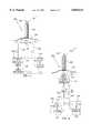
- FIGS. 1A-1Cillustrate mixing and modulating method embodiments of the invention.
- FIG. 1Ais a block diagram 20 which illustrates a method of generating intermodulation products of first and second electronic signals 22 and 24 and inserting them into an optical carrier signal 26.
- the optical carrier signal 26is amplified through an optical amplifier 30 which has a nonlinear transfer function between its optical input port 32 and its optical output port 34.
- the optical amplifier 30is preferably an SOA whose junction is forward biased with a bias current I B that is applied through an amplifier bias port 36 (I B is typically on the order of 50 milliamps).
- I Bis typically on the order of 50 milliamps.
- the first and second electronic signals 22 and 24are combined in an adder 38 and coupled to the bias port 36.
- the nonlinear transfer functioncauses an amplified optical signal 40 at the optical output port 34 to be modulated by the first and second electronic signals 22 and 24 and their intermodulation products.
- a photodetector 42will, therefore, not only generate amplitude-scaled versions of the first and second electronic signals 22 and 24, but will also generate their intermodulation products at a photodetector output 44.
- FIG. 2illustrates an exemplary spectrum 50 at the photodetector output 44 when the first and second electronic signals 22 and 24 have angular frequencies ⁇ 1 and ⁇ 2 which differ by a delta frequency 51.
- the spectrum 50includes amplitude-scaled versions 52 and 54 of the first and second electronic signals.
- the spectrumalso includes a difference signal 56 having an angular frequency ⁇ 1 - ⁇ 2 , a sum signal 58 having an angular frequency ⁇ 1 + ⁇ 2 , a third order product 60 having an angular frequency 2 ⁇ 1 - ⁇ 2 , and a fourth-order product 61 having an angular frequency 3 ⁇ 1 - ⁇ 2 .
- the spectrum 50has a second harmonic 62 (angular frequency 2 ⁇ 1 ) of the first electronic signal 22 and a second harmonic 64 (angular frequency 2 ⁇ 2 ) of the second electronic signal 24.
- the process illustrated in FIG. 1Ais especially suited for generating intermodulation products (e.g., signals 56, 58, 60 and 62 of FIG. 2) of radio frequency signals (e.g., microwave and millimeter-wave signals) in an optical carrier signal.
- the adder 38can be a conventional microwave or millimeter-wave power combiner and the bias current I B can be coupled through an adder 66 in the form of a conventional bias tee.
- FIG. 1BAnother method of generating intermodulation products of first and second electronic signals in an optical carrier is shown in the block diagram 80 of FIG. 1B.
- FIG. 1Bis similar to FIG. 1A with like elements indicated by like reference numbers.
- the first electronic signalcontinues to be coupled to the bias port 36 of the optical amplifier 30 but the second electronic signal 24 is introduced through the optical input port 32.
- the optical carrier signal 26 and the second electronic signal 24are coupled respectively to an optical input port and a modulation port of an optical modulator 82.
- the amplitude modulated optical signalis then applied at the optical input port 32.
- Intermodulation products of first and second electronic signals in an optical carriercan also be generated by a method which is shown in the block diagram 90 of FIG. 1C.
- FIG. 1Cis similar to FIG. 1A with like elements indicated by like reference numbers.
- the first and second electronic signalsare both coupled to the modulation port of the optical modulator 82 so that they modulate the optical carrier signal 26.
- the amplitude modulated optical signalis then applied at the optical input port 32.
- the spectrum 50 of FIG. 2is representative of the spectrum at the photodetector output 44 for all three processes.
- the intermodulation products of FIG. 2are exemplary ones only, other intermodulation products of these processes have amplitudes and/or frequencies which do not appear in the limited spectrum of FIG. 2.
- the signal levels shownare a function of the drive levels of the first and second electronic signals 22 and 24.
- FIGS. 1A-1Care especially suited for converting the frequency of electronic signals. This is illustrated in FIG. 1B by the addition of a filter 84 that is connected to the output 44 of the photodetector 42.
- the filter 84is configured to filter a selected intermodulation product from the composite detected signal at the photodetector output 44.
- the block diagram 80represents an upconverter if the filter 84 is configured to pass only the sum signal 58, i.e., one of the first and second electronic signals 22 and 24 can be used to upconvert the other.
- the block diagram 80represents a downconverter if the filter 84 is configured to pass only the difference signal 56, i.e., one of the first and second electronic signals 22 and 24 can be used to downconvert the other.
- optical signal 26 and the modulated, amplified optical signal 40are coupled to and from the optical amplifier 30 with optical fibers 88.
- the optical amplifier 30can be positioned remotely from other process elements, e.g., the photodetectors 42, the modulator 82 and laser sources, without incurring significant signal loss.
- These processesare preferably practiced with optical wavelengths at which optical fibers, optical amplifiers and laser sources are readily available, e.g., 1300 and 1550 nanometers.
- any nonlinear optical amplifiercan be used to practice the teachings of the invention, the semiconductor fabrication techniques for SOA's facilitate their integration into semiconductor chips of optoelectronic systems.
- the interconnecting optical fibersmust be expensive polarization-maintaining optical fibers. Costs can be considerably reduced (especially for long runs of fibers) if the teachings of the invention are practiced with polarization-insensitive SOA's.
- An exemplary polarization-insensitive SOAis described in Newirk, M. A., et al., "1.5 um Multiquantum-Well Semiconductor Optical Amplifier with Tensile and Compressively Strained Wells for Polarization-Independent Gain", IEEE Photonics Letters, Vol. 4, No. 4, April, 1993.
- An exemplary photodetector for use in FIGS. 1A-1Cis a PIN photodiode and an exemplary optical modulator is a directional coupler or Mach-Zehnder modulator formed with optical waveguides diffused into a lithium niobate substrate.
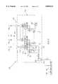
- FIGS. 3-6illustrate phased-array antenna embodiments of the invention.
- FIG. 3illustrates a phased-array receiving antenna 100 whose operation includes the intermodulation generating process illustrated in FIG. 1A.
- the phased-array antenna 100has an antenna array 102 which includes an array of receptive elements 104 that are each configured to receive a portion 106 of a radio-frequency signal.
- the antenna arrayalso includes a plurality of the optical amplifiers 30 and a plurality of the photodetectors 42 of FIGS. 1A-1C.
- Each of the optical amplifiers 30has its bias port 36 coupled to a respective one of the receptive elements 104 to receive its radio-frequency signal portion 106.
- Each of the photodetectors 42is coupled to the optical output port 34 of a respective one of the optical amplifiers 30.
- each of the optical amplifiers 30provides an optical input port 32 for insertion of an optical signal from a laser 107.
- the optical signalis modulated by the radio-frequency signal portion 106 that is received at that optical amplifier's bias port 36.
- This amplified and modulated optical signalis then detected by the photodetector 42 at that optical amplifier's optical output port 34 to recover the radio-frequency signal portion 106.
- Each of the optical amplifiers 30 of the antenna array 102also provides an optical input port 32 and a bias port 36 for insertion at either of a local oscillator signal for frequency converting that optical amplifier's radio-frequency signal portion 106.
- the local oscillator signalis generated by a local oscillator signal generator 112 and this signal is coupled to each of the bias ports 36 through a respective phase shifter 114.
- the radio frequency portion 106 from each receptive element 104is amplified by a radio-frequency low-noise amplifier 116 and this amplified signal is combined with the phase-shifted local oscillator signal 110 in a conventional radio-frequency combiner 118.
- the transmission lines coupling the local oscillator generator 112 to the combiners 118form a corporate feed, i.e., they have equal lengths.
- the detected radio-frequency output from the photodetectors 42is filtered by bandpass filters 120 and coupled into a signal processor 122 for a variety of conventional processing steps (e.g., further downconversion and amplification followed by demodulation to recover information content).
- the optical signal from the laser 107is coupled to the optical input ports 32 of the optical amplifiers 30 by a primary optical fiber 124, an optical fiber splitter 125 (e.g., a fused biconical taper coupler) and a plurality of secondary optical fibers 126.
- the amplified and modulated optical signals at the optical output ports 34 of the optical amplifiers 30are coupled to the photodetectors 42 by optical fibers 128.
- the radio-frequency signal portions 106 and the phase shifted local oscillator signals 110are coupled into the bias ports 36 of the optical amplifiers 30.
- the phase shifts (e.g., ⁇ 1 , ⁇ 2 , - - - ⁇ N ) of the phase shifters 114are selected to create an effective receive phase front 132 in the radio-frequency signal portions 106.
- the phased-array antenna 100will have its receive pattern steered along a beam axis 134 which is orthogonal to the phase front 132. With appropriate selection of the phase shifts of the phase shifters 114, the receive pattern can be steered in selected directions. All of the optical fibers 128 preferably have the same length to maintain the antenna phasing.
- the photodetectors 42are functionally part of the antenna array 102, they may also be positioned along with the laser 107, the bandpass filters 120 and the signal processor 122 at a remote location. In a large shipboard phased-array antenna, for example, this remote location would typically be below decks and only the other portions of the antenna array 102 would be positioned in an exposed location.
- the modulating processes of the inventionpermit these separate locations to be coupled together with low-loss optical fibers, e.g., the fibers 124 and 128.
- the operational frequency band of the phased-array antenna 100can be at a wide range of radio-frequencies, e.g., microwave frequency or millimeter-wave frequency.
- An exemplary set of frequenciesis 24 GHz for the radio-frequency signal portions 106 (the portions of the received antenna beam) and 22 GHz for the local oscillator signal 110.
- the difference frequency 56 in FIG. 2would be 2 GHz.
- the bandpass filters 120 of FIG. 3would be designed to pass this downconverted signal 56 on to the signal processor 122 for further processing.
- the process illustrated in FIG. 1Acan therefore be used to provide a convenient intermediate frequency for further processing in the signal processor 122 of FIG. 3. It is difficult and expensive to build photodetectors that demodulate very high modulation frequencies, e.g., >20 GHz. By downconverting the modulation to lower frequencies, the process of FIG. 1A also relaxes the frequency requirements of photodetectors.
- FIG. 5illustrates a phased-array receiving antenna 160 (and an antenna array 162) whose operation includes the intermodulation generating process illustrated in FIG. 1B.
- FIG. 5is similar to FIG. 3 with like elements indicated by like reference numbers.
- the local oscillator 112couples its local oscillator signal into a bias port 164 of the laser 107.
- the laser's optical signalcould be modulated as shown in FIG. 1B, i.e., by coupling the local oscillator signal 110 into an optical modulator 82 which is driven by the laser 107.
- radio-frequency phase shifters 114 of FIG. 3are replaced by optical time-delay systems 166 which are positioned in each secondary optical fiber 126.
- Various conventional optical time-delay systemscan be used.
- An exemplary oneincludes a plurality of optical waveguides which have different path lengths. These different path lengths are selected with optical switches, e.g., directional coupler switches. The different path lengths introduce different time delays (hence, phase delays of the local oscillator modulation) into the secondary optical fibers 126 (and into the frequency-converted signals in the optical fibers 128).
- the secondary optical fibers 126would typically be structured to form a corporate feed to the optical amplifiers 30, i.e., their physical lengths would be equal.
- the radio-frequency signal portions 106are coupled into the bias ports 36 of the optical amplifiers 30 and phase shifted local oscillator signals are coupled into the optical input ports 32 of the optical amplifiers 30.
- the receive direction 134 of the antenna 160can be steered by moving the optical time-delay systems 166 to the output optical fibers 128 (as indicated by broken lines).
- Various other steering embodimentscan be formed.
- the laser 107can be coupled by separate optical fibers to each optical amplifier 30.
- An optical modulatore.g., modulator 82 of FIG. 1B
- antenna steeringcan also be accomplished with selective phase shifts applied in the signal processor 122 to the outputs of the bandpass filters 120.
- FIG. 6illustrates a phased-array transmitting antenna 170 (and an antenna array 172) whose operation includes the intermodulation generating process illustrated in FIG. 1B.
- FIG. 6is similar to FIG. 3 with like elements indicated by like reference numbers.
- the receptive elements 104are used as radiative elements.
- antenna elementshave the property of reciprocity, i.e., the characteristics of an antenna element are the same whether it is transmitting or receiving.
- An antenna element which has a particular receive patterninherently has the same radiative pattern.
- the low noise receive amplifiers 116are replaced by bandpass filters 174 and transmitting power amplifiers 175 and the outputs of the photodetectors 42 are coupled to the bandpass filters 174.
- the optical modulator 82(of FIG. 1B) is positioned in the primary optical fiber 124 to receive the output of the laser 107.
- the secondary optical fibers 126preferably form a corporate feed, i.e., they have equal lengths. These lengths were not of concern in FIG. 3 because the optical signal did not carry a modulation.
- the local oscillator 112continues to be coupled to the bias ports 36 of the optical amplifiers 30 by a plurality of phase shifters 114.
- a radio-frequency signal(typically referred to as an intermediate frequency or IF) is inserted into the modulating port of the modulator 82.
- this IF signalmixes with a local oscillator signal from the local oscillator signal generator 112.
- a modulated and amplified optical signal from each optical amplifier 30is detected by its respective photodetector 42.
- One of the intermodulation productse.g., the sum signal 58 of FIG. 2, is passed through a respective bandpass filter 174. This signal is amplified by a respective power amplifier 175 and radiated by a respective radiative element 104 as a transmitted signal portion 176.
- phase shiftse.g., ⁇ 1 , ⁇ 2 , - - - ⁇ N
- the phase shifts of the phase shifters 114are selected to create an effective transmit phase front 182 so that the total transmitted power will have a transmit pattern steered along a beam axis 184 which is orthogonal to the phase front 182.
- the transmit patterncan be steered in selected directions.
- the structure of the antenna 170permits the elements of the antenna array 172 to be positioned adjacent an antenna aperture 188 and other elements, e.g., the laser 107 and the modulator 82, can be positioned remotely and connected to the array by the low-loss primary optical fiber 124.
- FIG. 7illustrates a phased-array transmitting antenna 190 (and an antenna array 192) whose operation includes the intermodulation generating process illustrated in FIG. 1C.
- FIG. 7is similar to FIG. 6 with like elements indicated by like reference numbers.
- a plurality of optical combiners 198 and optical time-delay fibersare used to couple the lasers 107 and 194 to the secondary optical fibers 126.
- the optical time-delay fibersare arranged to introduce a predetermined time delay into the optical signals (hence, a predetermined phase delay of modulation carried by these signals).
- a time-delay fiber 200introduces a predetermined time delay between two adjacent secondary optical fibers 126 of the optical signal from the laser 107.
- a time-delay fiber 202introduces a predetermined time delay between two adjacent secondary optical fibers 126 of the optical signal from the laser 194.
- an IF signalis inserted into the modulating port of the modulator 82 and a local oscillator signal is inserted into the bias port of the laser 194.
- These signalsare carried to the optical amplifiers 30.
- a modulated and amplified optical signal from each optical amplifier 30is detected by its respective photodetector 42.
- One of the intermodulation productse.g., the sum signal 58 of FIG. 2, is passed through a respective bandpass filter 174. This signal is amplified by a respective power amplifier 175 and radiated by a respective radiative element 104 as a transmitted signal portion 176.
- the predetermined time delays of the time-delay optical fibers 200 and 202can be selected in a conventional manner to create the effective transmit phase front 182 so that the total transmitted power from the radiative elements 104 will have a transmit pattern steered along a beam axis 184 which is orthogonal to the phase front 182.
- the fixed time-delay fibers 200 and 202cause the beam axis 184 to have a fixed direction. This direction can be selected by introducing the optical time-delay systems 166 (of FIG. 5) into one of the time-delay fibers 200 and 202 (as indicated by broken lines).
- the time delays of optical fibers 200 and 202can be fixed and the local oscillator and IF frequencies varied to steer the beam axis 184 at a fixed transmitted frequency.
- the local oscillator and IF frequenciescan be varied in a coordinated way so that their sum is constant and equal to the desired transmitted frequency.
- the phase between antenna elements 104will then vary as the difference between the local oscillator and IF frequencies which allows the beam to be steered in angle. This method of antenna steering was taught in U.S. Pat. No. 3,090,928 issued to Welty, W. R.
- FIGS. 8 and 9illustrate remote antenna system embodiments of the invention.
- FIG. 8illustrates a remote antenna system 220 whose operation includes the intermodulation generating process illustrated in FIG. 1B.
- An optical amplifier 30(see FIG. 1B) has its bias port 36 connected to an antenna 222 which is positioned on a tower 224 at a remote location, e.g., a mountain peak 226.
- the optical amplifier's optical input port 32is connected by an optical fiber 228 to a laser 107 (see FIG. 3) which is located at a signal processing site 230.
- a local oscillator signal generator 112(see FIG. 5) is connected to a bias port 164 of the laser 107.
- a series arrangement of a photodetector 42, a bandpass filter 120 and a signal processor 122(see FIG. 3) is also positioned at the signal processing site 230 and connected to the optical amplifier's optical output port 34 by an optical fiber 234.
- an optical signal from the laser 107is modulated by a local oscillator signal from the local oscillator signal generator 112.
- This modulated signalis coupled to the optical input port of the optical amplifier 30 and a received radio-frequency signal 236 (from a communication satellite, for example) is coupled from the antenna 222 to the optical amplifier's bias port 36.
- Thisgenerates an amplified, modulated laser signal that is coupled from the optical amplifier's optical output port 34 to the photodetector 42 which recovers a spectrum similar to that of FIG. 2.
- An intermodulation producte.g., the difference signal 56 of FIG. 2
- a low-noise amplifiercan be positioned between the antenna 222 and the optical amplifier's bias port 36.
- the system 220couples the remote antenna 222 and the processing site 230 with low-loss optical fibers and eliminates the need for radio-frequency mixing structures at the remote site 226.
- the system 220can downconvert the received signal 236 to a difference frequency that is in the photodetector's range.
- FIG. 9illustrates a remote antenna system 240 whose operation includes the intermodulation generating process illustrated in FIG. 1C.
- FIG. 9is similar to FIG. 8 with like elements indicated by like reference numbers.
- the optical amplifier 30now has its optical output port 34 connected through a serial arrangement of the photodetector 42, a bandpass filter 174 and a power amplifier 175 (see FIG. 7) to the antenna 222.
- Another laser 242is located at another signal processing site 244 that is removed from the signal processing site 230 and from the remote site 226.
- the laser 242is also coupled to the optical amplifier's optical input port 32 through an optical fiber 246 and an optical combiner 248.
- an IF signal 249modulates the laser signal of the laser 242 and this signal mixes in the optical amplifier 30 with the local oscillator signal from the local oscillator signal generator 112.
- the intermodulation productsare detected by the photodetector 42, filtered by the bandpass filter 174 to pass a selected product, e.g., the sum signal 58 of FIG. 2.
- This selected intermodulation productis amplified by the power amplifier 175 and radiated from the antenna as an antenna beam 250.
- the frequency of the radiated signal 250 at a transmitting site 226can be controlled from either of the distant processing sites 230 and 244.
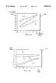
- FIGS. 1A-1CThe methods shown in FIGS. 1A-1C for generating intermodulation products were tested in exemplary laboratory setups. The general spectrum of these products is illustrated in FIG. 2. Specific product levels obtained in one test of the process of FIG. 1A are shown in the graph 260 of FIG. 10. The horizontal graph axis indicates power levels applied to the bias port 36 of the optical amplifier 30 of FIG. 1A and the vertical graph axis indicates detected powers at the output 44 of the photodetector 42. Although the test was conducted with an available polarization-sensitive SOA (Hewlett Packard 3100-1550), its results are representative of the performance of polarization-sensitive SOA's.
- Hewlett Packard 3100-1550Hewlett Packard 3100-1550
- the laser signal wavelengthwas 1540 nanometers
- input power to the SOAwas -20 dBm
- the SOA's optical gainwas 5.9 dB.
- the first and second electronic signals 22 and 24 of FIG. 1Awere set with angular frequencies ⁇ 1 , and ⁇ 2 equal to 490 MHz and 510 MHz respectively.
- the levels of the detected signals 51 and 52 of FIG. 2are shown as plot 51/52.
- the detected difference signal 56 and third-order intermodulation signal 60are shown as plots 56 and 60 respectively.
- the intermodulation productsare reduced (e.g., ⁇ 25 dB) indicating that the SOA is particularly useful as a modulator in this region, i.e., modulating the optical carrier with one of the first and second electronic signals 22 and 24.
- the intermodulation productsrise (e.g., the difference signal 60 approaches the signals 51 and 52) indicating that the SOA is particularly useful as an intermodulation product generator in this region.
- Link and conversion gains obtained in one test of the process of FIG. 1Bare shown in the graph 270 of FIG. 11.
- the first and second electronic signals 22 and 24 of FIG. 1Bwere set with angular frequencies ⁇ 1 and ⁇ 2 equal to 250 MHz and 230 MHz respectively.
- the first electronic signal 22was applied to the bias port of a semiconductor optical amplifier and the second electronic signal 24 was applied to the bias port of a laser operating at a wavelength of 1541.5 nanometers (application of the second electronic signal is in contrast to FIG. 1B in which it is applied to a modulator 82).
- the horizontal graph axisindicates different signal levels of the second electronic signal 24.
- Plot 56indicates the conversion gain of the difference signal having a frequency of ⁇ 1 - ⁇ 2 and plot 58 indicates the conversion gain of the sum signal having a frequency of ⁇ 1 + ⁇ 2 .
- These conversion gainsare shown as a function of the signal level of the second electronic signal 24 as the level of the first electronic signal 22 was held constant at -20 dBm.
- the conversion gainsincrease linearly with the signal level of the second electronic signal 24 until they plateau in the region of -45 dB for signal levels (of the second electronic signal 24) above ⁇ -4 dBm.
- these plot reference numbersare the same as those for the difference and sum signals of FIG. 2.
- Plot 52indicates the link gain of the first electronic signal 22 and plot 54 indicates the link gain of the second electronic signal 24.
- plot reference numbersare the same as those for the first electronic signal ( ⁇ 1 ), and second electronic signal ( ⁇ 2 ) of FIG. 2.
- the gain G(t)is used in this expression for the optical polarization density which acts as a source in Maxwell's equations. Using the slowly varying envelope approximation, one obtains a well-known solution ##EQU3##
- the degree of linearity of the deviceis determined by the relative magnitude of the second and third order terms with respect to the fundamental.
- SOA'sare capable of generating higher order harmonics and intermodulation signals of the form of ##EQU4##
- the amplitude of the RF drivebecomes large, then the time dependent term in the exponential is such that a series expansion will become inaccurate. In this case, higher order terms can play an important role in the process of frequency conversion.
- the relative order of magnitudecan then be found by a Fourier filtering process. For example, the difference frequency term becomes ##EQU5##
- Nonlinear optical amplifiersgenerate intermodulation products of radio-frequency signals in an optical carrier without the penalty of an optical conversion loss and without the need for radio-frequency mixers, electro-optic modulators and expensive polarization-maintaining optical fibers.
- SOA'scan be used as the nonlinear optical amplifiers to facilitate integration with other system structures on semiconductor chips.
- polarization-insensitive SOA'savoids the cost of polarization-maintaining optical fibers.
- Nonlinear optical amplifierscan be easily integrated into optoelectronic systems because electronic signals can be coupled into either their bias ports or their optical input ports.
Landscapes
- Physics & Mathematics (AREA)
- Electromagnetism (AREA)
- Engineering & Computer Science (AREA)
- Computer Networks & Wireless Communication (AREA)
- Signal Processing (AREA)
- Optical Communication System (AREA)
- Variable-Direction Aerials And Aerial Arrays (AREA)
Abstract
Description
Claims (50)
Priority Applications (1)
| Application Number | Priority Date | Filing Date | Title |
|---|---|---|---|
| US08/803,963US5859611A (en) | 1997-02-21 | 1997-02-21 | Mixing and modulating methods and structures using nonlinear optical amplifiers |
Applications Claiming Priority (1)
| Application Number | Priority Date | Filing Date | Title |
|---|---|---|---|
| US08/803,963US5859611A (en) | 1997-02-21 | 1997-02-21 | Mixing and modulating methods and structures using nonlinear optical amplifiers |
Publications (1)
| Publication Number | Publication Date |
|---|---|
| US5859611Atrue US5859611A (en) | 1999-01-12 |
Family
ID=25187861
Family Applications (1)
| Application Number | Title | Priority Date | Filing Date |
|---|---|---|---|
| US08/803,963Expired - LifetimeUS5859611A (en) | 1997-02-21 | 1997-02-21 | Mixing and modulating methods and structures using nonlinear optical amplifiers |
Country Status (1)
| Country | Link |
|---|---|
| US (1) | US5859611A (en) |
Cited By (45)
| Publication number | Priority date | Publication date | Assignee | Title |
|---|---|---|---|---|
| US20010021047A1 (en)* | 1999-12-24 | 2001-09-13 | Hiroyuki Sasai | Optical transmission system and optical receiver |
| US6362906B1 (en)* | 1998-07-28 | 2002-03-26 | Raytheon Company | Flexible optical RF receiver |
| US6466165B2 (en)* | 2000-06-16 | 2002-10-15 | Kabushiki Kaisha Toshiba | Adaptive array antenna |
| US20020186436A1 (en)* | 2001-06-08 | 2002-12-12 | Sanjay Mani | Method and apparatus for multiplexing in a wireless communication infrastructure |
| US20020191565A1 (en)* | 2001-06-08 | 2002-12-19 | Sanjay Mani | Methods and systems employing receive diversity in distributed cellular antenna applications |
| US20030090767A1 (en)* | 2001-11-15 | 2003-05-15 | Hrl Laboratories, Llc | Agile RF-lightwave waveform synthesis and an optical multi-tone amplitude modulator |
| US6587256B2 (en)* | 2001-06-06 | 2003-07-01 | Northrop Grumman Corporation | RF combiner based on cascaded optical phase modulation |
| US6614591B1 (en)* | 2002-06-06 | 2003-09-02 | The Boeing Company | Optical combiner |
| US20030197918A1 (en)* | 2002-04-17 | 2003-10-23 | Hrl Laboratories, Llc | Integrated optical circuit for effecting stable injection locking of laser diode pairs used for microwave signal synthesis |
| US6731829B2 (en)* | 2000-12-16 | 2004-05-04 | Hrl Laboratories, Llc. | True-time all-optical delay generator for array beam steerers |
| WO2004053518A1 (en)* | 2002-12-11 | 2004-06-24 | Qinetiq Limited | Laser radar apparatus having multiple output wavelenghts |
| US6766158B1 (en)* | 2001-03-30 | 2004-07-20 | Skyworks Solutions, Inc. | Harmonic cancellation mixer |
| US20040198453A1 (en)* | 2002-09-20 | 2004-10-07 | David Cutrer | Distributed wireless network employing utility poles and optical signal distribution |
| US6826163B2 (en) | 2001-06-08 | 2004-11-30 | Nextg Networks | Method and apparatus for multiplexing in a wireless communication infrastructure |
| US6826164B2 (en) | 2001-06-08 | 2004-11-30 | Nextg Networks | Method and apparatus for multiplexing in a wireless communication infrastructure |
| US20040264977A1 (en)* | 2001-11-15 | 2004-12-30 | Daniel Yap | Method and apparatus for waveform generation |
| US20050013612A1 (en)* | 2003-07-14 | 2005-01-20 | Hrl Laboratories, Llc | Multiple wavelength photonic oscillator |
| US20050052726A1 (en)* | 2003-08-14 | 2005-03-10 | Fibest, Ltd. | Optical module and optical communication system |
| US20050163171A1 (en)* | 2004-01-27 | 2005-07-28 | Hrl Laboratories, Llc | Wavelength reconfigurable laser transmitter tuned via the resonance passbands of a tunable microresonator |
| US20050168247A1 (en)* | 2004-01-30 | 2005-08-04 | The Regents Of The University Of California | Electrical transient sampling system using a regenerative gain-clamped fiber optic delay line |
| US6963442B2 (en) | 2002-04-17 | 2005-11-08 | Hrl Laboratories, Llc | Low-noise, switchable RF-lightwave synthesizer |
| US20060022872A1 (en)* | 2004-07-30 | 2006-02-02 | Integrinautics Corporation | Asynchronous local position determination system and method |
| US20060022870A1 (en)* | 2004-07-30 | 2006-02-02 | Integrinautics Corporation | Land-based local ranging signal methods and systems |
| US20060022873A1 (en)* | 2004-07-30 | 2006-02-02 | Integrinautics Corporation | Synchronizing ranging signals in an asynchronous ranging or position system |
| US20060022869A1 (en)* | 2004-07-30 | 2006-02-02 | Integirnautics Corporation | Analog decorrelation of ranging signals |
| US20060022871A1 (en)* | 2004-07-30 | 2006-02-02 | Integrinautics Corporation | Land-based transmitter position determination |
| US7271766B2 (en) | 2004-07-30 | 2007-09-18 | Novariant, Inc. | Satellite and local system position determination |
| US20070285308A1 (en)* | 2004-07-30 | 2007-12-13 | Integirnautics Corporation | Multiple frequency antenna structures and methods for receiving navigation or ranging signals |
| EP1971036A1 (en)* | 2007-03-14 | 2008-09-17 | Dtu | A method and a device for detection of a first signal superimposed on a second signal |
| US20090115658A1 (en)* | 2004-07-30 | 2009-05-07 | Integrinautics Corporation | Distributed radio frequency ranging signal receiver for navigation or position determination |
| US7965211B1 (en)* | 2009-11-09 | 2011-06-21 | Rockwell Collins, Inc. | High power DAC power amplifier |
| US8400355B1 (en)* | 2008-04-04 | 2013-03-19 | Ipitek, Inc. | Passive photonic dense wavelength-division multiplexing true-time-delay system |
| US8515285B2 (en) | 2011-07-25 | 2013-08-20 | Harris Corporation | RF communications device including an optical link and related devices and methods |
| US8526817B2 (en) | 2012-01-24 | 2013-09-03 | Harris Corporation | Communications device with discriminator for generating intermediate frequency signal and related methods |
| US8620158B2 (en) | 2012-01-24 | 2013-12-31 | Harris Corporation | Communications device with discriminator and wavelength division multiplexing for generating intermediate frequency signal and related methods |
| US8842992B2 (en) | 2012-03-07 | 2014-09-23 | Harris Corporation | Electro-optic communications device with frequency conversion and related methods |
| US8879919B2 (en) | 2011-09-09 | 2014-11-04 | Harris Corporation | Photonic communications device with an FM/PM discriminator and related methods |
| US20140376921A1 (en)* | 2013-06-21 | 2014-12-25 | Northrop Grumman Systems Corporation | Optical channelizer for w-band detection |
| US9548878B2 (en) | 2008-03-12 | 2017-01-17 | Hypres, Inc. | Digital radio frequency transceiver system and method |
| US9859678B2 (en) | 2014-09-23 | 2018-01-02 | Harris Corporation | Communications device with optical injection locking source and related methods |
| US20190064332A1 (en)* | 2017-08-24 | 2019-02-28 | Toyota Motor Engineering & Manufacturing North America, Inc. | Photonics integrated phase measurement |
| US11183770B2 (en)* | 2019-05-17 | 2021-11-23 | Raytheon Company | Dual polarization RF antenna feed module and photonic integrated circuit (PIC) |
| US11463174B1 (en)* | 2017-11-07 | 2022-10-04 | Magiq Technologies, Inc. | RF processing system and method |
| CN115842590A (en)* | 2021-09-21 | 2023-03-24 | 苹果公司 | Electronic device with high frequency multi-mode communication capability |
| US12287235B2 (en)* | 2009-05-27 | 2025-04-29 | Silixa Ltd. | Method and apparatus for optical sensing |
Citations (6)
| Publication number | Priority date | Publication date | Assignee | Title |
|---|---|---|---|---|
| US3090928A (en)* | 1958-01-02 | 1963-05-21 | Hughes Aircraft Co | Apparatus for generating plurality of signals having variable phase difference |
| US5166821A (en)* | 1991-03-12 | 1992-11-24 | General Instrument Corporation | Reduction of non-linear effects in optical fiber communication systems and method of using same |
| US5323406A (en)* | 1992-11-02 | 1994-06-21 | Yee Ting K | Photonic mixer for photonically multiplying two electrical signals in two optically interconnected interferometric modulators operated at modulation outside the linear range |
| US5617239A (en)* | 1992-06-29 | 1997-04-01 | British Telecommunications Public Limited Comany | Optical source for communications system |
| US5687261A (en)* | 1996-01-24 | 1997-11-11 | California Institute Of Technology | Fiber-optic delay-line stabilization of heterodyne optical signal generator and method using same |
| US5710651A (en)* | 1995-12-13 | 1998-01-20 | California Institute Of Technology | Remote millimeter-wave antenna fiber optic communication system using dual optical signal with millimeter-wave beat frequency |
- 1997
- 1997-02-21USUS08/803,963patent/US5859611A/ennot_activeExpired - Lifetime
Patent Citations (6)
| Publication number | Priority date | Publication date | Assignee | Title |
|---|---|---|---|---|
| US3090928A (en)* | 1958-01-02 | 1963-05-21 | Hughes Aircraft Co | Apparatus for generating plurality of signals having variable phase difference |
| US5166821A (en)* | 1991-03-12 | 1992-11-24 | General Instrument Corporation | Reduction of non-linear effects in optical fiber communication systems and method of using same |
| US5617239A (en)* | 1992-06-29 | 1997-04-01 | British Telecommunications Public Limited Comany | Optical source for communications system |
| US5323406A (en)* | 1992-11-02 | 1994-06-21 | Yee Ting K | Photonic mixer for photonically multiplying two electrical signals in two optically interconnected interferometric modulators operated at modulation outside the linear range |
| US5710651A (en)* | 1995-12-13 | 1998-01-20 | California Institute Of Technology | Remote millimeter-wave antenna fiber optic communication system using dual optical signal with millimeter-wave beat frequency |
| US5687261A (en)* | 1996-01-24 | 1997-11-11 | California Institute Of Technology | Fiber-optic delay-line stabilization of heterodyne optical signal generator and method using same |
Non-Patent Citations (4)
| Title |
|---|
| Logan, Ronald T., et al., "Millimeter-Wave Photonic Downconverters: Theory and Demonstration", Proceedings of SPIE Conference on Optical Technology for Microwave Applications VII, Jul. 9-14, 1995. |
| Logan, Ronald T., et al., Millimeter Wave Photonic Downconverters: Theory and Demonstration , Proceedings of SPIE Conference on Optical Technology for Microwave Applications VII , Jul. 9 14, 1995.* |
| Newirk, M.A., et al., "1.5 um Multiquantum-Well Semiconductor Optical Amplifier with Tensile and Compressively Strained Wells for Polarization-Independent Gain", IEEE Photonics Letters, vol. 4, No. 4, Apr. 1993. |
| Newirk, M.A., et al., 1.5 um Multiquantum Well Semiconductor Optical Amplifier with Tensile and Compressively Strained Wells for Polarization Independent Gain , IEEE Photonics Letters , vol. 4, No. 4, Apr. 1993.* |
Cited By (74)
| Publication number | Priority date | Publication date | Assignee | Title |
|---|---|---|---|---|
| US6362906B1 (en)* | 1998-07-28 | 2002-03-26 | Raytheon Company | Flexible optical RF receiver |
| US20010021047A1 (en)* | 1999-12-24 | 2001-09-13 | Hiroyuki Sasai | Optical transmission system and optical receiver |
| US6650292B2 (en) | 2000-06-16 | 2003-11-18 | Kabushiki Kaisha Toshiba | Adaptive array antenna |
| US6466165B2 (en)* | 2000-06-16 | 2002-10-15 | Kabushiki Kaisha Toshiba | Adaptive array antenna |
| US20030016173A1 (en)* | 2000-06-16 | 2003-01-23 | Shuichi Obayashi | Adaptive array antenna |
| US6750817B2 (en)* | 2000-06-16 | 2004-06-15 | Kabushiki Kaisha Toshiba | Adaptive array antenna |
| US6731829B2 (en)* | 2000-12-16 | 2004-05-04 | Hrl Laboratories, Llc. | True-time all-optical delay generator for array beam steerers |
| US6766158B1 (en)* | 2001-03-30 | 2004-07-20 | Skyworks Solutions, Inc. | Harmonic cancellation mixer |
| US6587256B2 (en)* | 2001-06-06 | 2003-07-01 | Northrop Grumman Corporation | RF combiner based on cascaded optical phase modulation |
| US20020191565A1 (en)* | 2001-06-08 | 2002-12-19 | Sanjay Mani | Methods and systems employing receive diversity in distributed cellular antenna applications |
| US7127175B2 (en) | 2001-06-08 | 2006-10-24 | Nextg Networks | Method and apparatus for multiplexing in a wireless communication infrastructure |
| US20020186436A1 (en)* | 2001-06-08 | 2002-12-12 | Sanjay Mani | Method and apparatus for multiplexing in a wireless communication infrastructure |
| US6826163B2 (en) | 2001-06-08 | 2004-11-30 | Nextg Networks | Method and apparatus for multiplexing in a wireless communication infrastructure |
| US6826164B2 (en) | 2001-06-08 | 2004-11-30 | Nextg Networks | Method and apparatus for multiplexing in a wireless communication infrastructure |
| US7085499B2 (en) | 2001-11-15 | 2006-08-01 | Hrl Laboratories, Llc | Agile RF-lightwave waveform synthesis and an optical multi-tone amplitude modulator |
| US20030090767A1 (en)* | 2001-11-15 | 2003-05-15 | Hrl Laboratories, Llc | Agile RF-lightwave waveform synthesis and an optical multi-tone amplitude modulator |
| US7650080B2 (en) | 2001-11-15 | 2010-01-19 | Hrl Laboratories, Llc | Method and apparatus for waveform generation |
| US20040264977A1 (en)* | 2001-11-15 | 2004-12-30 | Daniel Yap | Method and apparatus for waveform generation |
| US6963442B2 (en) | 2002-04-17 | 2005-11-08 | Hrl Laboratories, Llc | Low-noise, switchable RF-lightwave synthesizer |
| US6867904B2 (en) | 2002-04-17 | 2005-03-15 | Hrl Laboratories, Llc | Integrated optical circuit for effecting stable injection locking of laser diode pairs used for microwave signal synthesis |
| US20030197918A1 (en)* | 2002-04-17 | 2003-10-23 | Hrl Laboratories, Llc | Integrated optical circuit for effecting stable injection locking of laser diode pairs used for microwave signal synthesis |
| US6614591B1 (en)* | 2002-06-06 | 2003-09-02 | The Boeing Company | Optical combiner |
| US20040198453A1 (en)* | 2002-09-20 | 2004-10-07 | David Cutrer | Distributed wireless network employing utility poles and optical signal distribution |
| WO2004053518A1 (en)* | 2002-12-11 | 2004-06-24 | Qinetiq Limited | Laser radar apparatus having multiple output wavelenghts |
| US7349094B2 (en) | 2002-12-11 | 2008-03-25 | Qinetiq Limited | Laser radar apparatus having multiple output wavelengths |
| US20050013612A1 (en)* | 2003-07-14 | 2005-01-20 | Hrl Laboratories, Llc | Multiple wavelength photonic oscillator |
| US7499653B2 (en) | 2003-07-14 | 2009-03-03 | Hrl Laboratories, Llc | Multiple wavelength photonic oscillator |
| US7911686B2 (en)* | 2003-08-14 | 2011-03-22 | Fibest, Ltd. | Optical module and optical communication system |
| US20050052726A1 (en)* | 2003-08-14 | 2005-03-10 | Fibest, Ltd. | Optical module and optical communication system |
| US7822082B2 (en) | 2004-01-27 | 2010-10-26 | Hrl Laboratories, Llc | Wavelength reconfigurable laser transmitter tuned via the resonance passbands of a tunable microresonator |
| US20050163171A1 (en)* | 2004-01-27 | 2005-07-28 | Hrl Laboratories, Llc | Wavelength reconfigurable laser transmitter tuned via the resonance passbands of a tunable microresonator |
| US20050168247A1 (en)* | 2004-01-30 | 2005-08-04 | The Regents Of The University Of California | Electrical transient sampling system using a regenerative gain-clamped fiber optic delay line |
| US20070285308A1 (en)* | 2004-07-30 | 2007-12-13 | Integirnautics Corporation | Multiple frequency antenna structures and methods for receiving navigation or ranging signals |
| US20060022872A1 (en)* | 2004-07-30 | 2006-02-02 | Integrinautics Corporation | Asynchronous local position determination system and method |
| US20070115176A1 (en)* | 2004-07-30 | 2007-05-24 | Novariant, Inc. | Land-based local ranging signal methods and systems |
| US7271766B2 (en) | 2004-07-30 | 2007-09-18 | Novariant, Inc. | Satellite and local system position determination |
| US20060279461A1 (en)* | 2004-07-30 | 2006-12-14 | Novariant, Inc. | Land-based local ranging signal methods and systems |
| US7315278B1 (en) | 2004-07-30 | 2008-01-01 | Novariant, Inc. | Multiple frequency antenna structures and methods for receiving navigation or ranging signals |
| US7339524B2 (en) | 2004-07-30 | 2008-03-04 | Novariant, Inc. | Analog decorrelation of ranging signals |
| US7339525B2 (en) | 2004-07-30 | 2008-03-04 | Novariant, Inc. | Land-based local ranging signal methods and systems |
| US7339526B2 (en) | 2004-07-30 | 2008-03-04 | Novariant, Inc. | Synchronizing ranging signals in an asynchronous ranging or position system |
| US7342538B2 (en) | 2004-07-30 | 2008-03-11 | Novariant, Inc. | Asynchronous local position determination system and method |
| US7345627B2 (en) | 2004-07-30 | 2008-03-18 | Novariant, Inc. | Land-based local ranging signal methods and systems |
| US20060022871A1 (en)* | 2004-07-30 | 2006-02-02 | Integrinautics Corporation | Land-based transmitter position determination |
| US7382318B2 (en) | 2004-07-30 | 2008-06-03 | Novariant Inc. | Land-based local ranging signal methods and systems |
| US7205939B2 (en) | 2004-07-30 | 2007-04-17 | Novariant, Inc. | Land-based transmitter position determination |
| US20060022870A1 (en)* | 2004-07-30 | 2006-02-02 | Integrinautics Corporation | Land-based local ranging signal methods and systems |
| US20060022869A1 (en)* | 2004-07-30 | 2006-02-02 | Integirnautics Corporation | Analog decorrelation of ranging signals |
| US20090115658A1 (en)* | 2004-07-30 | 2009-05-07 | Integrinautics Corporation | Distributed radio frequency ranging signal receiver for navigation or position determination |
| US7532160B1 (en)* | 2004-07-30 | 2009-05-12 | Novariant, Inc. | Distributed radio frequency ranging signal receiver for navigation or position determination |
| US20060022873A1 (en)* | 2004-07-30 | 2006-02-02 | Integrinautics Corporation | Synchronizing ranging signals in an asynchronous ranging or position system |
| US8428464B2 (en) | 2007-03-14 | 2013-04-23 | Dtu, Technical University Of Denmark | Methods and devices for detection of a first signal superimposed on a second signal |
| WO2008110169A1 (en)* | 2007-03-14 | 2008-09-18 | Dtu, Technical University Of Denmark | A method and a device for detection of a first signal superimposed on a second signal |
| EP1971036A1 (en)* | 2007-03-14 | 2008-09-17 | Dtu | A method and a device for detection of a first signal superimposed on a second signal |
| US20100142963A1 (en)* | 2007-03-14 | 2010-06-10 | Dtu, Technical University Of Denmark | Methods and Devices for detection of a first signal superimposed on a second signal |
| US10382132B2 (en) | 2008-03-12 | 2019-08-13 | Hypres, Inc. | Digital radio frequency transceiver system and method |
| US9548878B2 (en) | 2008-03-12 | 2017-01-17 | Hypres, Inc. | Digital radio frequency transceiver system and method |
| US8400355B1 (en)* | 2008-04-04 | 2013-03-19 | Ipitek, Inc. | Passive photonic dense wavelength-division multiplexing true-time-delay system |
| US12287235B2 (en)* | 2009-05-27 | 2025-04-29 | Silixa Ltd. | Method and apparatus for optical sensing |
| US7965211B1 (en)* | 2009-11-09 | 2011-06-21 | Rockwell Collins, Inc. | High power DAC power amplifier |
| US8515285B2 (en) | 2011-07-25 | 2013-08-20 | Harris Corporation | RF communications device including an optical link and related devices and methods |
| US8879919B2 (en) | 2011-09-09 | 2014-11-04 | Harris Corporation | Photonic communications device with an FM/PM discriminator and related methods |
| US8526817B2 (en) | 2012-01-24 | 2013-09-03 | Harris Corporation | Communications device with discriminator for generating intermediate frequency signal and related methods |
| US8620158B2 (en) | 2012-01-24 | 2013-12-31 | Harris Corporation | Communications device with discriminator and wavelength division multiplexing for generating intermediate frequency signal and related methods |
| US8842992B2 (en) | 2012-03-07 | 2014-09-23 | Harris Corporation | Electro-optic communications device with frequency conversion and related methods |
| US11108470B2 (en) | 2013-06-21 | 2021-08-31 | Northrop Grumman Systems Corporation | Optical channelizer for W-band detection |
| US20140376921A1 (en)* | 2013-06-21 | 2014-12-25 | Northrop Grumman Systems Corporation | Optical channelizer for w-band detection |
| US10447409B2 (en)* | 2013-06-21 | 2019-10-15 | Northrop Grumman Systems Corporation | Optical channelizer for W-band detection |
| US9859678B2 (en) | 2014-09-23 | 2018-01-02 | Harris Corporation | Communications device with optical injection locking source and related methods |
| US10627496B2 (en)* | 2017-08-24 | 2020-04-21 | Toyota Motor Engineering & Manufacturing North America, Inc. | Photonics integrated phase measurement |
| US20190064332A1 (en)* | 2017-08-24 | 2019-02-28 | Toyota Motor Engineering & Manufacturing North America, Inc. | Photonics integrated phase measurement |
| US11463174B1 (en)* | 2017-11-07 | 2022-10-04 | Magiq Technologies, Inc. | RF processing system and method |
| US11183770B2 (en)* | 2019-05-17 | 2021-11-23 | Raytheon Company | Dual polarization RF antenna feed module and photonic integrated circuit (PIC) |
| CN115842590A (en)* | 2021-09-21 | 2023-03-24 | 苹果公司 | Electronic device with high frequency multi-mode communication capability |
Similar Documents
| Publication | Publication Date | Title |
|---|---|---|
| US5859611A (en) | Mixing and modulating methods and structures using nonlinear optical amplifiers | |
| US5710651A (en) | Remote millimeter-wave antenna fiber optic communication system using dual optical signal with millimeter-wave beat frequency | |
| US7483600B2 (en) | Integrated coherent optical detector | |
| Sun et al. | Efficient microwave frequency conversion using photonic link signal mixing | |
| US5543805A (en) | Phased array beam controller using integrated electro-optic circuits | |
| US7835650B2 (en) | Optical domain frequency down-conversion of microwave signals | |
| EP1561259B1 (en) | Optically and frequency scanned array | |
| Zhang et al. | Broadband microwave photonic sub-harmonic downconverter with phase shifting ability | |
| Kong et al. | Microwave photonic image-reject mixer based on a tunable microwave photonic filter with high rejection | |
| Drummond et al. | Dimensioning of a multibeam coherent photonic beamformer fed by a phased array antenna | |
| Wang et al. | Filter-free photonic image-rejection down-conversion for distributed antenna applications | |
| US10812197B1 (en) | Pulsed Sagnac loop phase-modulated microwave photonic link | |
| Seeds | Optical technologies for phased array antennas | |
| US7269354B1 (en) | Superheterodyne photonic receiver using non-serial frequency translation | |
| US6313792B1 (en) | Optical control device for electronic scanning antenna | |
| Birkmayer et al. | Proof-of-concept model of a coherent optical beam-forming network | |
| Nagatsuma et al. | Photonic generation of millimeter and terahertz waves and its applications | |
| US4868894A (en) | System for transmitting microwave signals via an optical link | |
| Woo et al. | Feedforward Compensation of Laser Frequency and Phase Noise for Photonics-Based Sub-THz Generation | |
| Paul | Optical beam forming and steering for phased-array antenna | |
| Yao | Polarization insensitive antenna remoting link with frequency conversion gain | |
| CN115208475B (en) | Up-down frequency conversion integrated broadband radio frequency front-end system and radio frequency signal receiving and transmitting method | |
| US5467414A (en) | Device for generating feedback signals to regulate optical monitoring circuits (PLL) | |
| Liu et al. | Millimeter wave beamsteering with true time delayed integrated optical beamforming network | |
| WO2003081811A1 (en) | Method of up-conversion of all-optical signal through cross-gain modulation in semiconductor optical amplifier and apparatus thereof |
Legal Events
| Date | Code | Title | Description |
|---|---|---|---|
| AS | Assignment | Owner name:HUGHES ELECTRONICS, CALIFORNIA Free format text:ASSIGNMENT OF ASSIGNORS INTEREST;ASSIGNORS:LAM, JUAN F.;STEPHENS, RONALD R.;TANGONAN, GREGORY L.;REEL/FRAME:008422/0764;SIGNING DATES FROM 19970211 TO 19970213 | |
| AS | Assignment | Owner name:HUGHES ELECTRONICS CORPORATION, CALIFORNIA Free format text:ASSIGNMENT OF ASSIGNORS INTEREST;ASSIGNOR:HE HOLDINGS INC., DBA HUGHES ELECTRONICS, FORMERLY KNOWN AS HUGHES AIRCRAFT COMPANY;REEL/FRAME:008927/0928 Effective date:19971217 | |
| STCF | Information on status: patent grant | Free format text:PATENTED CASE | |
| AS | Assignment | Owner name:AIR FORCE, UNITED STATES, NEW YORK Free format text:CONFIRMATORY LICENSE;ASSIGNOR:HUGHES ELECTRONICS CORPORATION;REEL/FRAME:011660/0903 Effective date:20010321 | |
| FEPP | Fee payment procedure | Free format text:PAYOR NUMBER ASSIGNED (ORIGINAL EVENT CODE: ASPN); ENTITY STATUS OF PATENT OWNER: LARGE ENTITY Free format text:PAYER NUMBER DE-ASSIGNED (ORIGINAL EVENT CODE: RMPN); ENTITY STATUS OF PATENT OWNER: LARGE ENTITY | |
| FPAY | Fee payment | Year of fee payment:4 | |
| REMI | Maintenance fee reminder mailed | ||
| FPAY | Fee payment | Year of fee payment:8 | |
| FPAY | Fee payment | Year of fee payment:12 |