US5859518A - Switched reluctance motor controller with sensorless rotor position detection - Google Patents
Switched reluctance motor controller with sensorless rotor position detectionDownload PDFInfo
- Publication number
- US5859518A US5859518AUS08/996,084US99608497AUS5859518AUS 5859518 AUS5859518 AUS 5859518AUS 99608497 AUS99608497 AUS 99608497AUS 5859518 AUS5859518 AUS 5859518A
- Authority
- US
- United States
- Prior art keywords
- motor
- phase
- series
- rotor
- coupled
- Prior art date
- Legal status (The legal status is an assumption and is not a legal conclusion. Google has not performed a legal analysis and makes no representation as to the accuracy of the status listed.)
- Expired - Lifetime
Links
- 238000001514detection methodMethods0.000title1
- 239000003990capacitorSubstances0.000claimsabstractdescription39
- 230000004044responseEffects0.000claimsabstractdescription20
- 238000000034methodMethods0.000claimsdescription43
- 230000008859changeEffects0.000claimsdescription6
- 230000000977initiatory effectEffects0.000claimsdescription4
- 230000002401inhibitory effectEffects0.000claimsdescription3
- 238000004804windingMethods0.000abstractdescription84
- 230000005284excitationEffects0.000abstractdescription37
- 230000007423decreaseEffects0.000abstractdescription7
- 238000005259measurementMethods0.000abstractdescription4
- 101100464782Saccharomyces cerevisiae (strain ATCC 204508 / S288c) CMP2 geneProteins0.000description21
- 230000001965increasing effectEffects0.000description11
- 101100464779Saccharomyces cerevisiae (strain ATCC 204508 / S288c) CNA1 geneProteins0.000description9
- 238000010586diagramMethods0.000description6
- 230000001939inductive effectEffects0.000description5
- 230000008569processEffects0.000description5
- 206010048669Terminal stateDiseases0.000description3
- 230000000694effectsEffects0.000description3
- 230000006698inductionEffects0.000description3
- 238000004519manufacturing processMethods0.000description3
- 230000002441reversible effectEffects0.000description3
- 230000003797telogen phaseEffects0.000description3
- 230000000737periodic effectEffects0.000description2
- 230000007704transitionEffects0.000description2
- 230000005355Hall effectEffects0.000description1
- 230000002411adverseEffects0.000description1
- 230000003321amplificationEffects0.000description1
- 238000013459approachMethods0.000description1
- 238000010276constructionMethods0.000description1
- 238000012937correctionMethods0.000description1
- 230000008878couplingEffects0.000description1
- 238000010168coupling processMethods0.000description1
- 238000005859coupling reactionMethods0.000description1
- 230000003247decreasing effectEffects0.000description1
- 230000001419dependent effectEffects0.000description1
- 238000001914filtrationMethods0.000description1
- 230000004907fluxEffects0.000description1
- 230000010354integrationEffects0.000description1
- 238000003475laminationMethods0.000description1
- 230000002045lasting effectEffects0.000description1
- 238000012986modificationMethods0.000description1
- 230000004048modificationEffects0.000description1
- 238000003199nucleic acid amplification methodMethods0.000description1
- 230000010355oscillationEffects0.000description1
- 230000002829reductive effectEffects0.000description1
- 230000003252repetitive effectEffects0.000description1
Images


Classifications
- H—ELECTRICITY
- H02—GENERATION; CONVERSION OR DISTRIBUTION OF ELECTRIC POWER
- H02P—CONTROL OR REGULATION OF ELECTRIC MOTORS, ELECTRIC GENERATORS OR DYNAMO-ELECTRIC CONVERTERS; CONTROLLING TRANSFORMERS, REACTORS OR CHOKE COILS
- H02P6/00—Arrangements for controlling synchronous motors or other dynamo-electric motors using electronic commutation dependent on the rotor position; Electronic commutators therefor
- H02P6/14—Electronic commutators
- H02P6/16—Circuit arrangements for detecting position
- H02P6/18—Circuit arrangements for detecting position without separate position detecting elements
- H02P6/185—Circuit arrangements for detecting position without separate position detecting elements using inductance sensing, e.g. pulse excitation
- H—ELECTRICITY
- H02—GENERATION; CONVERSION OR DISTRIBUTION OF ELECTRIC POWER
- H02P—CONTROL OR REGULATION OF ELECTRIC MOTORS, ELECTRIC GENERATORS OR DYNAMO-ELECTRIC CONVERTERS; CONTROLLING TRANSFORMERS, REACTORS OR CHOKE COILS
- H02P25/00—Arrangements or methods for the control of AC motors characterised by the kind of AC motor or by structural details
- H02P25/02—Arrangements or methods for the control of AC motors characterised by the kind of AC motor or by structural details characterised by the kind of motor
- H02P25/08—Reluctance motors
- H02P25/086—Commutation
- H02P25/089—Sensorless control
Definitions
- the inventionrelates to the field of controllers for switched reluctance motors. More particularly, the invention relates to a controller for a switched reluctance motor wherein a rotational position of a rotor of the motor is detected by the controller without the use of a position sensor.
- Switched reluctance motorsare characterized in that torque is produced by the tendency of the rotor to align with an excited stator winding, thereby maximizing the inductance of the excited winding.
- both the rotor and the statorhave unequal numbers of evenly spaced poles.
- the poles of the statorare wound with field windings, whereas, the poles of the rotor are not wound.
- Each pair of stator poles positioned opposite each otherhave field windings that are electrically coupled in series or in parallel so that both field windings are excited simultaneously, thus, comprising a phase of the motor.
- each phaseis driven, typically by applying a DC excitation voltage, in an appropriate sequence according to the position of the rotor. This process of driving the phases in sequence is referred to as commutation.
- FIGS. 1A-Cillustrate a sequence of side sectional views of a switched reluctance motor during counterclockwise rotation of the rotor 10.
- the rotor poles 1 and 3are aligned with the stator 12 poles A and A' (phase A).
- the windings LA of phase Ahave a maximum value of inductance. Therefore, to move the rotor 10 into the position illustrated in FIG. 1A, phase A is driven by applying an excitation voltage across the windings LA of phase A, thereby inducing a current in the windings LA of phase A.
- phase Aremains excited while the rotor 10 continues to turn past the position of alignment illustrated in FIG. 1A, however, a torque would be produced in a direction opposite the direction of rotation.
- the excitation voltageis preferably removed from phase A prior to the rotor 10 reaching this position of alignment illustrated in FIG. 1A.
- the number of degrees of rotation between removing the excitation voltage from a phase and alignment of the rotor 10 with the corresponding phaseis referred to as the phase advance.
- FIG. 1Billustrates the rotor 10 continuing to turn beyond alignment of the rotor 10 poles 1 and 3 with phase A and towards alignment of the rotor 10 poles 2 and 4 with phase B.
- the excitation voltagePrior to reaching alignment with phase B, as illustrated in FIG. 1C, the excitation voltage is removed from phase B and an excitation voltage is applied to the windings LC of the stator 12 poles C and C' (phase C). Note that as illustrated in FIG. 1C, the inductance of the windings LB of phase B is at a maximum value.
- the excitation voltagePrior to the alignment of the rotor 10 poles 1 and 3 with phase C, the excitation voltage is removed from phase C and an excitation voltage is applied to phase A. This commutation process continues, thereby maintaining continuous rotation of the rotor 10.
- Switched reluctance motorsdiffer from brushless DC motors in that switched reluctance motors do not utilize permanent magnets.
- the use of permanent magnets in the rotor of a typical brushless DC motortends to increase production costs and can lead to operational problems should the magnets loosen or vibrate.
- the rotor of a switched reluctance motorcan be relatively inexpensively manufactured from stamped sheet laminations.
- each field winding of a switched reluctance motoris driven independently of the other field windings, whereas, the field windings of a brushless DC motor typically share common terminals, being connected in a delta or wye configuration.
- Switched reluctance motorsdiffer from AC induction motors in that AC induction motors generally include field windings in the rotor which tend to increase the cost of producing AC induction motors. As noted above, switched reluctance motors do not have rotor windings.
- switched reluctance motorsWhile switched reluctance motors have relatively low production costs in comparison to other types of motors, they tend to be difficult to control, requiring complicated driving circuitry. This is because the relationships between torque, field current, speed, and optimal phase advance tend to be highly non-linear and also tend to vary with the load.
- the rotor positionFor driving a switched reluctance motor, knowledge of the rotor position is generally required for appropriately commutating the motor.
- the rotor positionhas been determined by position sensors mounted to the rotor shaft. For example, the use of encoders, Hall effect sensors, and sensing transformers are known. These sensors can increase the cost and complexity of such a system and reduce its reliability.
- U.S. Pat. No. 4,520,302discloses a drive circuit for a stepping motor. Current through a phase winding that is next in sequence to be driven is allowed to increase for fixed period of time determined by a clock pulse length. Rotor position is detected by comparing a value of current attained at the end of this fixed period of time to a preset value. The preset value is set by adjusting a potentiometer. When the preset value is exceeded, the phase is energized.
- This techniquehas a disadvantage in that the current at the end of the fixed period of time must be increasing for each successive clock pulse.
- the inductance of a phase winding that is about to be energizedcan also decrease while the previous phase is still being driven.
- U.S. Pat. No. 4,868,4708discloses an energizing system for a switched-type reluctance motor. High frequency pulses of short duration are fed to power transistors in the energizing circuit of that phase winding which is next in line for excitation. Commutation to the next phase is performed by comparing observed values to a preset value, similarly to U.S. Pat. No. 4,520,302, described above. U.S. Pat. No. 4,868,478, however discloses that a correction factor is calculated in an attempt to account for variations in the applied motor voltage, drive current and load. Accordingly, this technique does not overcome all the limitations of U.S. Pat. No. 4,520,302. In addition, the expense and complexity of the system disclosed by U.S. Pat. No. 4,868,478, is increased by its suggested use of a microprocessor.
- the inventionis a controller for a switched reluctance motor that does not utilize a sensor for detecting the rotational position of the rotor.
- Each pair of stator poles positioned opposite each otherhave field windings that are electrically coupled in series or in parallel so that both field windings are excited simultaneously, thus, comprising a phase of the motor.
- each phaseis driven by applying an excitation voltage in an appropriate sequence according to the position of the rotor.
- the rotortends to align with an excited phase.
- poles of the rotorare aligned with poles of the stator, the inductance of the windings of the aligned stator poles reach a maximum value.
- this minimum value for a phaseoccurs when the rotor is midway between positions of alignment of the remaining two phases.
- the rotational position of the rotor of the motoris determined by measuring the inductance of each phase during periods when the minimum level of inductance for the phase is expected to occur. This is accomplished by applying a series of voltage pulses to the appropriate field winding during the appropriate period while current levels produced in response to the voltage pulses are measured. The relationship between applied voltage, measured current, and time, is utilized to determine the inductance value as it decreases and then increases between positions of rotor alignment. Commutation to a next phase is performed based upon the observed inductance value. More particularly, a first voltage pulse is applied to an appropriate field winding after a commutation. A level of current induced by the first voltage pulse is stored across a capacitor.
- additional voltage pulsesare applied which induce additional current levels. These current levels are compared to a predetermined threshold. Once a current level exceeds the predetermined threshold, subsequent current levels are compared to the stored level. Upon a subsequent current level which does not exceed the stored level, commutation to a next phase is performed. Waiting until after the predetermined threshold is exceeded before performing a commutation prevents the motor from being commutated inappropriately in the event that the rotor is stationary or moving slowly.
- the number of degrees of rotation between removing the excitation voltage from a phase and alignment of the rotor with the corresponding phaseis the phase advance.
- the phase advanceis adjusted by controlling an offset value utilized for comparing the subsequent current levels to the stored value.
- the offset valueis preferably controlled to be proportional to the speed of rotation of the rotor.
- FIGS. 1A-Cillustrate a sequence of side sectional views of a switched reluctance motor during counterclockwise rotation of the rotor.
- FIG. 2illustrates a power inverter according to the present invention for driving a switched reluctance motor.
- FIGS. 3A-Cillustrate current waveforms according to the present invention for driving a switched reluctance motor and for sensing rotor position versus time during rotation of the motor.
- FIG. 4illustrates how the current spikes induced in a phase are utilized to determine when to commutate so as to begin driving the phase.
- FIG. 5illustrates how the current spikes induced in a phase are utilized to determine when to commutate so as to begin driving the phase according to an adjustable phase advance.
- FIG. 6illustrates a schematic block diagram of a circuit for sensing the position of the rotor and for initiating commutation of the motor at appropriate times according to the position of the rotor.
- FIG. 7illustrates a schematic block diagram of a controller circuit according to the present invention for driving a switched reluctance motor.
- FIG. 8illustrates a schematic diagram of the comparator CMP2 illustrated in FIG. 6.
- FIG. 2illustrates a power inverter 50 according to the present invention for driving a three-phase switched reluctance motor.
- a supply voltage VMTRis coupled to a source of a PMOSFET Q1A and to a cathode of a diode D1A.
- a control terminal PAis coupled to an input terminal of a high side driver UA.
- An output terminal of the high side driver UAis coupled to a gate of the transistor Q1A.
- a drain of the transistor Q1Ais coupled to a first terminal of a field winding LA (around the poles A and A') of the motor and to a cathode of a diode D2A.
- a second terminal of the field winding LAis coupled to a drain of an NMOSFET Q2A and to an anode of the diode D1A.
- a control terminal NAis coupled to a gate of the transistor Q2A.
- a source of the transistor Q2Ais coupled to a first terminal of a resistor R1A and to a first terminal of a resistor R2A.
- a second terminal of the resistor R2Ais coupled to a first terminal of a capacitor C1A and to a current sense terminal ISNSA.
- a second terminal of the capacitor C1A, a second terminal of the resistor R1A and an anode of the diode D2Aare coupled to a ground node GNDA.
- the supply voltage VMTRis also coupled to a source of a PMOSFET Q1B and to a cathode of a diode D1B.
- a control terminal PBis coupled to an input terminal of a high side driver UB.
- An output terminal of the high side driver UBis coupled to a gate of the transistor Q1B.
- a drain of the transistor Q1Bis coupled to a first terminal of a field winding LB (around the poles B and B') of the motor and to a cathode of a diode D2B.
- a second terminal of the field winding LBis coupled to a drain of an NMOSFET Q2B and to an anode of the diode D1B.
- a control terminal NBis coupled to a gate of the transistor Q2B.
- a source of the transistor Q2Bis coupled to a first terminal of a resistor R1B and to a first terminal of a resistor R2B.
- a second terminal of the resistor R2Bis coupled to a first terminal of a capacitor C1B and to a current sense terminal ISNSB.
- a second terminal of the capacitor C1B, a second terminal of the resistor R1B and an anode of the diode D2Bare also coupled to a ground node GNDB.
- the supply voltage VMTRis also coupled to a source of a PMOSFET Q1C and to a cathode of a diode D1C.
- a control terminal PCis coupled to an input terminal of a high side driver UC.
- An output terminal of the high side driver UCis coupled to a gate of the transistor Q1C.
- a drain of the transistor Q1Cis coupled to a first terminal of a field winding LC (around the poles C and C') of the motor and to a cathode of a diode D2C.
- a second terminal of the field winding LCis coupled to a drain of an NMOSFET Q2C and to an anode of the diode D1C.
- a control terminal NCis coupled to a gate of the transistor Q2C.
- a source of the transistor Q2Cis coupled to a first terminal of a resistor R1C and to a first terminal of a resistor R2C.
- a second terminal of the resistor R2Cis coupled to a first terminal of a capacitor C1C and to a current sense terminal ISNSC.
- a second terminal of the capacitor C1C, a second terminal of the resistor R1C and an anode of the diode D2Care also coupled to a ground node GNDC.
- the transistors Q1A and Q2Aare turned on by applying a logical high voltage to each of the control terminals PA and NA.
- the high side driver UAconverts the logical high voltage applied to the terminal PA into a low level suitable for driving the transistor Q1A in saturation.
- the transistors Q1A and Q2Aare turned on, the voltage supply VMTR is effectively coupled across the field winding LA. In response, a current IA through the field winding LA ramps up.
- FIGS. 3A-Cillustrate current waveforms for driving a switched reluctance motor and for sensing rotor position versus time during rotation of the motor.
- Excitation of phase Ais illustrated in FIG. 3A where the current IA is shown to begin ramping up before alignment of the rotor with Phase C at time t1.
- FIG. 3Aillustrates that in a drive phase, the current IA ramps up to a terminal value T.
- the terminal value T for IAdepends upon the level of the voltage VMTR and upon the on-resistance of the transistors Q1A and Q2A, the resistance of the field windings LA and the value of the resistor R1A.
- the ramp-up time for IAalso depends upon the inductance of the field windings LA. As explained herein, however, the voltage applied during the drive phase can be modulated for controlling the speed of the motor. In which case, the IA can follow a different curve during the drive phase.
- phase AAs illustrated in FIG. 3, alignment of the rotor with phase C occurs at the time t1.
- the current in phase Apreferably begins ramping up prior to the time t1 by an amount of time which depends upon the amount of phase advance. Applying the excitation voltage to phase A at the appropriate time tends to cause the rotor to continue rotation so as to align with phase A.
- Alignment of the rotor with phase Acoincides with the time t2 illustrated in FIG. 3. Note that as the rotor approaches alignment with phase A, the inductance of the field winding LA increases until reaching a maximum value at the time t2 when the rotor is aligned with phase A. Then, the inductance of field winding LA decreases during a rest phase A.
- the transistors Q1A and Q2Aare turned off by applying a logical low voltage to the terminals PA and NA.
- the diodes D1A and D2A(FIG. 2) are provided for shunting the current IA which is stored in the field winding LA to the supply voltage VMTR. Because the current IA cannot instantaneously fall to zero, the excitation voltage is preferably removed from phase A prior to the time t2, as illustrated in FIG. 3A by the current IA beginning to ramp down prior to the time t2.
- the amount of time prior to t2 that the excitation voltage is removedpreferably also depends upon the phase advance.
- an excitation voltageis applied to phase B by applying a logical high voltage to the terminals PB and NB.
- a current IB through the field winding LBramps up.
- This excitation of phase Bis illustrated in FIG. 3B where the current IB is shown ramping up to a terminal value T.
- Applying the excitation voltage to phase B at the appropriate timetends to cause the rotor to align with phase B. Alignment of the rotor with phase B coincides with the time t3 illustrated in FIG. 3. Accordingly, the excitation voltage is preferably removed from phase B prior to the time t3, as illustrated in FIG. 3B by the current IB ramping down.
- an excitation voltageis applied to phase C by applying a logical high voltage to the terminals PC and NC.
- a current IC through the field winding LCramps up.
- This excitation of phase Cis illustrated in FIG. 3C where the current IC is shown ramping up to a terminal value T.
- Applying the excitation voltage to phase C at the appropriate timetends to cause the rotor to align with phase C. Alignment of the rotor with phase C coincides with the time t4 illustrated in FIG. 3. Accordingly, the excitation voltage is preferably removed from phase C prior to the time t4, as illustrated in FIG. 3C by the current IC ramping down.
- the inductance of the phase Areaches maximum level at the time t2 when the rotor is aligned with phase A.
- the inductance of phase Areaches a minimum level when the rotor is midway between alignment with phase B and with phase C.
- the inductance of the phase Breaches a maximum level at the time t3 when the rotor is aligned with phase B.
- the inductance of phase Breaches a minimum level when the rotor is midway between alignment with phase C and with phase A.
- the inductance of phase Creaches a maximum level at the times t1 and t4, when the rotor is in alignment with phase C.
- phase Creaches a minimum level when the rotor is midway between alignment with phase A and with phase B. Note that waveforms of the inductance values illustrated in FIG. 3 are typical and that the precise waveforms will depend upon the parameters of the particular switched reluctance motor being driven.
- the present inventiondetermines the position of the rotor of the motor by measuring the inductance of each phase of the motor during periods when the minimum level of inductance for the phase is expected to occur. This is accomplished by applying a series of voltage pulses to the appropriate field winding during a sense phase and measuring the current produced in response to the voltage pulses. The relationship between applied voltage, measured current, and time, is utilized to determine the inductance value as it decreases and then increases between positions of rotor alignment. Commutation to a next phase is performed based upon the observed inductance value.
- a current level value dependent upon the inductance valueis measured and stored after a commutation which occurs near in time to a position of alignment of the rotor. Then, subsequent measured current level values are compared to the stored value. Upon a subsequent measured current level value not exceeding the stored level, commutation to a next phase is performed. Because the stored value and the subsequent measured current level values are all observed values, no calibration is required. This is in contrast to prior systems, such as those disclosed in U.S. Pat. Nos. 4,520,302 and 4,868,478, which make the decision of when to commutate based upon a comparison of a measured value to a fixed value. In such a prior system, calibration of the fixed value is required for the system to operate.
- a measured current level valuemust rise above a predetermined threshold in addition to not exceeding the stored value. Waiting until after the measured current level value rises above the predetermined threshold before performing a commutation prevents the motor from being commutated inappropriately in the event that the rotor is stationary or moving slowly.
- the predetermined thresholdmust be calibrated, its precise value does not affect commutation so long as it falls within an appropriate range between the measured value and a maximum value attainable when the inductance of the winding is at a minimum.
- the current IAis measured by forming a voltage across the resistor R1A (FIG. 2) which is sensed via the terminal ISNSA.
- the resistor R2A and the capacitor C1Aform a low pass filter for filtering transients from the sensing signal formed at the terminal ISNSA.
- currents IB and ICare low pass filtered and sensed via terminals ISNSB and ISNSC, respectively.
- the sense phase for measuring of the inductance of the field windings LAbegins after the motor is commutated so as to begin driving phase C (at approximately the time t3 illustrated in FIG. 3).
- a logical high voltageis applied to the control terminals PA and NA (FIG. 2) in pulses, each pulse lasting a predetermined period of time.
- one or the other of the terminals PA and NAcan be held at a logical high voltage while the other of the terminals is pulsed.
- the transistors Q1A and Q2Aare both on for the predetermined period of time, coupling the supply voltage VMTR across the field winding LA of phase A. In response, the current IA in the field winding LA ramps up.
- the amount of time that the supply voltage VMTR is applied to the phase A for each pulse during the sense phase Ais shorter than the amount of time required for the current IA to reach a terminal value T during the drive phase A, thus, forming a series of current spikes.
- the height reached by of each of the spikes in the current IAis representative of the inductance of the field winding LA during the corresponding voltage pulse.
- Each current spikehas an amplitude that is inversely related to the inductance of the field winding LA during the corresponding interval.
- the amplitudes of the current spikesare utilized to determine the rotational position of the rotor and, thus, the amplitudes of the current spikes are utilized to determine when to commutate so as to begin driving phase A.
- the phase Ais in a rest period A.
- measurement of the inductance of the field windings LB of phase Bis performed after the rotor is commutated so as to begin the drive phase A (at approximately the time t1 illustrated in FIG. 3).
- a series of logical high voltage pulses of fixed durationto the control terminals PB and NB
- a series of current spikesare produced in the field winding LB, as illustrated in FIG. 3B.
- Each current spikehas an amplitude that is inversely related to the inductance of the field winding LB during the corresponding interval. Therefore, the amplitudes of the current spikes can be used to determine the rotational position of the rotor and, thus, the amplitudes of the current spikes are utilized to determine when to commutate so as to begin driving phase B.
- measurement of the inductance of the field windings LC of phase Cis performed after the motor is commutated so as to begin the drive phase B (at approximately the time t2 illustrated in FIG. 3).
- a series of logical high voltage pulses of fixed durationto the control terminals PC and NC, a series of current spikes are produced in the field winding LC, as illustrated in FIG. 3C.
- Each current spikehas an amplitude that is inversely related to the inductance of the field winding LC during the corresponding interval. Therefore, the amplitudes of the induced current spikes can be used to determine the rotational position of the rotor and, thus, the amplitudes of the current spikes are utilized to determine when to commutate so as to begin the drive phase C.
- the duration of the current spikesare selected to avoid producing a significant amount of torque on the rotor, but also to have sufficient amplitude so as to provide sufficient accuracy in measurement.
- the frequency at which the current spikes are induceddetermines the number of spikes which occur during each sense phase for a particular motor speed. A certain minimum number of current spikes are required for each sense phase to reliably determine the position of the rotor. Thus, the frequency at which the current spikes are induced is expected to determine the maximum motor speed.
- FIG. 4illustrates how the current spikes induced in a phase are utilized to determine when to commutate so as to begin driving the phase.
- a control signal COMMCLKis utilized to control commutation from driving a phase to driving a next phase in the sequence.
- a current spikeis induced in the field winding for the appropriate phase. For example, referring to FIG. 3, if the first pulse of COMMCLK results in phase A being driven, then current pulses are induced in phase B for measuring the inductance of phase B. Note that phase B is the phase next in sequence to be driven after phase A.
- the amplitude of the first induced current spikeis stored. This corresponds to Event 1 illustrated in FIG. 4.
- Event 1After storing the amplitude of the first current spike (Event 1), additional current spikes continue to be induced in the field winding. The amplitude of each of these current spikes is compared to a predetermined threshold VTHR. Eventually, as the inductance of the field winding drops, a current spike occurs having an amplitude that exceeds the predetermined threshold VTHR. This corresponds to Event 2. After a current spike occurs having an amplitude greater than the predetermined threshold (Event 2), additional current spikes continue to be induced in the field winding. The amplitude of each of these current spikes is compared to the amplitude of the first current spike stored (during Event 1).
- the time period elapsed between the two successive pulses in the control signal COMMCLKis equal to the time required for the rotor to rotate by thirty degrees mechanical.
- the time between the two successive pulses in the control signal COMMCLKis equal to the time required for the rotor to rotate by fifteen degrees mechanical. Therefore, the frequency of the signal COMMCLK is proportional to the speed of the motor.
- the process illustrated in FIG. 4repeats wherein a phase is driven and the inductance of a next phase is sensed by inducing current spikes in the next phase until another commutation is performed. After each commutation, a new value of an initial current spike is stored. In the example, if the inductance of phase B is being sensed, upon a current spike occurring having an amplitude lower than the amplitude of the first current spike (Event 3), the phase B will then become the drive state and the inductance of phase C will be sensed, as illustrated in FIG. 3.
- Event 2The current spikes occurring after Event 1 are compared to the threshold VTHR (Event 2) to ensure that the inductance falls and then rises again due to rotation of the rotor before commutating to a next phase (Event 3). Otherwise, if Event 2 was omitted, successive spikes having approximately the same amplitude, as occurs when the rotor is stationary or moving slowly, could cause a commutation to occur at an inappropriate time due to minor variations or noise in the current spikes. In an alternate embodiment, however, Event 2 can be omitted.
- the technique according to the present inventioncontrasts with prior systems where measured values are compared only to a fixed value to determine when to commutate the motor.
- the fixed valuemust be calibrated for the system to operate.
- the present inventiondoes compare measured values to a predetermined threshold VTHR, commutation is not based only upon this comparison. Rather, according to the present invention, commutation occurs when a measured value then falls below a previously measured and stored value. Because the stored value is a prior measured value, the technique according to the present invention is self-calibrating for each commutation.
- the current spikes which occur after Event 2are compared directly to the stored level obtained during Event 1. This results in a phase advance of approximately zero degrees.
- the phase advancewill vary somewhat for each commutation since the current spike (at Event 3) which is below the value stored during Event 1 (resulting in a commutation) can occur when the rotor is in a slightly different rotational position for each commutation depending upon the frequency of the current spikes relative to the motor speed. These variations can be reduced by increasing the frequency at which the current spikes are induced.
- phase advance of zero degreesis generally optimum only at low motor speeds such that the currents in the field windings have sufficient time to ramp down, thus, inducing only a small amount of torque in the direction opposite the direction of rotation of the rotor.
- the phase advanceshould generally be adjusted to ensure that the currents in the field windings have ramped down sufficiently so as to avoid inducing a significant amount of torque in the direction opposite rotation.
- FIG. 5illustrates how the current spikes induced in a phase are utilized to determine when to commutate according to an adjustable phase advance.
- a current spikeis induced in the field winding for the appropriate phase.
- the amplitude of the first current spikeis stored (Event 1).
- Event 1current spikes continue to be induced in the field winding.
- the amplitude of each of these current spikesis compared to a predetermined threshold VTHR.
- Event 2After Event 2 occurs, current spikes continue to be induced in the field winding.
- the amplitude of each of these current spikesis compared to the amplitude of the first current spike stored during Event 1, as adjusted by an offset voltage Vos.
- the offset voltage Vosdetermines the amount of phase advance. Therefore, the offset voltage is preferably adjusted according to the speed of the motor.
- the offset voltage Voscan be linearly proportional to the motor speed. Alternately, the offset voltage can have some other monotonic relationship to the motor speed.
- the offset voltage Vosis effectively added to the voltage stored during Event 1 to increase the level below which a subsequent current spike must fall to trigger a commutation (Event 3').
- Event 3'the control signal COMMCLK is pulsed, resulting in a commutation to a next phase.
- the processrepeats wherein the phase is driven and the inductance of a next phase is sensed by inducing current spikes until another commutation is performed.
- the phase advancemight not have a linearly proportional relationship to motor speed despite having an offset voltage that is linearly proportional to the motor speed. It is expected, however, that this will not result in significant adverse effects.
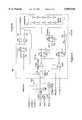
- FIG. 6illustrates a schematic block diagram of a circuit 100 for sensing the position of the rotor and for initiating commutation of the motor at appropriate times according to the position of the rotor.
- the terminal ISNSA(FIG. 2) is coupled to an input of an amplifier 102.
- An output of the amplifier 102is coupled to a drain of an NMOSFET 104.
- the terminal ISNSB(FIG. 2) is coupled to an input of an amplifier 106.
- An output of the amplifier 106is coupled to a drain of an NMOSFET 108.
- the terminal ISNSC(FIG. 2) is coupled to an input of an amplifier 110.
- An output of the amplifier 110is coupled to a drain of an NMOSFET 112.
- each of the amplifiers 102, 106 and 110provides amplification by a factor of five.
- a control terminal STATE Ais coupled to a gate of the transistor 108.
- a control terminal STATE Bis coupled to a gate of the transistor 112.
- a control terminal STATE Cis coupled to a gate of the transistor 104.
- a source of the transistor 104is coupled to a source of the transistor 108, to a source of the transistor 112, to a terminal ISNS, to a drain of an NMOSFET 116, to a non-inverting input of a comparator CMP1 and to an inverting input of a comparator CMP2.
- An inverting input of the comparator CMP1is coupled to a terminal VTHR.
- a terminal SNSCLKis coupled to an input of a logical inverter 118, to a first input of a logical NAND gate 120 and to a first input of a logical NAND gate 122.
- An output of the inverter 118is coupled to a clock input C of a flip-flop FF1.
- a data input D of the flip-flop FF1is coupled to receive a logical high voltage.
- a Q output of the flip-flop FF1is coupled to a second input of the logical NAND gate 120.
- a Q output of the flip-flop FF1is coupled to a second input of the logical NAND gate 122.
- An output of the NAND gate 120is coupled to an input of a logical inverter 124.
- An output of the NAND gate 122is coupled to an input of a logical inverter 126.
- An output of the inverter 126is coupled to a terminal HOLD1ST and to a gate of the transistor 116.
- a source of the transistor 116is coupled to a first terminal of a capacitor 128 and to a non-inverting input of the comparator CMP2.
- a second terminal of the capacitor 128is coupled to a ground node.
- An offset input of the comparator CMP2is coupled to a phase advance terminal PHADV.
- An output of the comparator CMP2is coupled to a data input of a flip-flop FF4.
- An output of the comparator CMP1is coupled to a data input of a flip-flop FF2.
- An output of the inverter 124is coupled to a terminal SNSREST and to an input of a logical inverter 130.
- An output of the inverter 130is coupled to a clock input C of the flip-flop FF2 and to a clock input C of the flip-flop FF4.
- a Q output of the flip-flop FF2is coupled to an input of a logical inverter 132.
- An output of the inverter 132is coupled to a clock input C of a flip-flop FF3.
- a data input D of the flip-flop FF3is coupled to receive a logical high voltage.
- a Q output of the flip-flop FF3is coupled to a terminal EVENT2.
- a Q output of the flip-flop FF3is coupled to a reset input R of the flip-flop FF4.
- a Q output of the flip-flop FF4is coupled to a terminal COMMCLK and to an input of a delay block 134.
- the delay block 134is preferably formed of an even number, in this case ten, of series coupled logical inverters.
- An output of the delay block 134is coupled to an input of a logical inverter 136.
- An output of the inverter 136is coupled to a first input of a logical NAND gate 138.
- a second input of the NAND gate 138is coupled to a terminal CLK1ST.
- An output of the NAND gate 138is coupled to a reset input R of the flip-flop FF1, to a reset input R of the flip-flop FF2 and to a reset input R of the flip-flop FF3.
- Terminals STATE A, STATE B and STATE Care configured to be a logical high voltage according to the motor phase that is being driven. For example, if phase A is being driven, STATE A is a logical high voltage. This turns on the transistor 108 which couples the signal ISNSB to the terminal ISNS via the amplifier 106.
- phase Bwhen phase A is being driven, phase B is selected to be sensed by the multiplexer 114.
- phase Cwhen phase B is being driven, phase C is being sensed and, when phase C is being driven, phase A is being sensed.
- the terminal SNSCLKis coupled to receive a clock signal SNSCLK.
- the clock signal SNSCLKhas a logical high voltage coincident with current pulses induced in each phase while the inductance of the phase is being sensed and a logical low voltage during intervals between the induced current pulses.
- the signal COMMCLKUpon a commutation of the motor, the signal COMMCLK is pulsed, as illustrated in FIGS. 4 and 5.
- the signal COMMCLKis applied to a finite state machine 202 (FIG. 7) for initiating a commutation of the motor and to the delay block 134.
- the output signal from the delay block 134(FIG. 6) is combined with a signal at the terminal CLK1ST by the NAND gate 138.
- the terminal CLK1STis coupled to receive a signal CLK1ST that is a logical low voltage initially, when the rotor position is unknown, then transitions to a logical high voltage after the rotor is in an initial state of pole pair alignment.
- the signal CLK1STremains logical high indefinitely after this initial transition from low to high.
- the flip-flops FF1, FF2 and FF3are reset by a logical high voltage pulse.
- the Q output of the flip-flop FF3holds the flip-flop FF4 in the reset state. Therefore, when the signal COMMCLK is a logical high voltage, the signal COMMCLK serves to reset the flip-flop FF4, thus, returning the signal COMMCLK to a logical low voltage.
- the delay block 134ensures that all the flip-flops FF1, FF2, FF3 and FF4, are not reset immediately, driving COMMCLK low, before the signal COMMCLK attains a logical high voltage.
- the Q output of the flip-flop FF1is a logical high voltage.
- This logical high voltageis combined by the NAND gate 122 with a logical high voltage of the signal SNSCLK while the first current spike is being induced.
- the terminal HOLD1STis a logical high voltage during the first induced current spike which occurs after a commutation. Therefore, the transistor 116 is turned on, allowing a voltage representative of the amplitude of the first current spike to be applied across the capacitor 128.
- the terminal HOLD1STbecomes a logical low voltage by the flip-flop FF1 being set after the pulse applied to the reset inputs of the flip-flops FF1, FF2 and FF3 is removed.
- a voltage representative of the maximum amplitude of the first current pulseis stored across the capacitor 128. This corresponds to Event 1 illustrated in FIGS. 4 and 5.
- the Q output of the flip-flop FF1is a logical high voltage which allows the clock signal SNSCLK to be applied to the clock inputs of the flip-flops FF2 and FF4.
- the clock signal SNSCLKprevents the states of the flip-flip flops FF2 and FF4 from being affected by the outputs of the comparators CMP1 and CMP2, respectively, except at the appropriate times during induced current spikes.
- the appropriate time for comparing each current spikeis a predetermined time interval after beginning inducement of the current spike. Accordingly, the relative amplitudes of the current spikes when they are compared by the comparators CMP1 and CMP2 are representative of the relative inductance levels of the field winding being sensed.
- the comparator CMP1monitors subsequent current spikes. Eventually, as the inductance of the motor phase being sensed falls, a current pulse will have an amplitude that exceeds the threshold voltage VTHR. This causes the output of the comparator CMP1 to change from a logical low voltage to a logical high voltage, coincident with the flip-flop FF2 being clocked. In response, the Q output of the flip-flop FF2 changes from a logical high voltage to a logical low voltage which, in turn, causes the Q output of the flip-flop FF3 to change from a logical high voltage to a logical low voltage. This removes the logical high voltage applied to the reset terminal of the flip-flop FF4. Removing the logical high voltage from the reset input R of the flip-flip FF4 enables the flip-flop FF4 to change states according to the output of the comparator CMP2. This corresponds to Event 2 illustrated in FIGS. 4 and 5.
- the comparator CMP2monitors subsequent current spikes.
- a voltage Vos representative of a desired amount of phase advanceis applied to a PHADV terminal of the comparator CMP2. This provides an offset for changing the logic level of the output of the comparator CMP2.
- the output of the comparator CMP2will then be a logical high voltage coincident with the flip-flop FF4 being clocked. This causes the Q output of the flip-flop FF4 and, thus, the signal COMMCLK to change from a logical low voltage to a logical high voltage. This corresponds to Events 3 and 3' illustrated in FIGS. 4 and 5, respectively. This process repeats for each phase of the motor.
- FIG. 7illustrates a schematic block diagram of a controller circuit 200 according to the present invention for driving a switched reluctance motor 204.
- the controller circuit 200is preferably an integrated circuit which is expected to be available under the Part Number ML4460 from Micro Linear Corporation, located at 2092 Concourse Drive, in San Jose, Calif.
- a first terminal of a capacitor 206is coupled to a ground node.
- a second terminal of the capacitor 206is coupled to an oscillator 208 via a terminal CSNS of the controller for setting the oscillation frequency of the oscillator 208.
- the oscillator 208provides the clock signal SNSCLK to the sense circuit 100 (also illustrated in FIG. 6), to the finite state machine 202 and to a start circuit 210.
- a first terminal of a capacitor 212is coupled to the ground node.
- a second terminal of the capacitor 212is coupled to CINIT terminal of the controller 200 and to the start circuit 210.
- the capacitor CINITsets timing for the excitation voltages applied to the motor 204 under control of the start circuit 210.
- the start circuit 210is coupled to the finite state machine 202 and to a commutation control logic circuit 214 for controlling excitation voltages applied to the motor 204 for starting the motor 204 from rest. Once the motor 204 begins turning, the sense circuit 100 takes over control.
- the sense circuit 100is coupled to provide the clock signal COMMCLK to the finite state machine 202, to a speed control circuit 216 and to a TACH OUT terminal of the controller 200.
- the finite state machine 202provides three control signals to the commutation control logic block 214.
- the three control signals, one for each phase of the motor 204,indicate at appropriate times that the commutation control logic block 214 is to control commutation from one phase to another.
- the commutation control logic block 214provides six control signals, one for each of the transistors Q1A, Q2A, Q1B, Q2B, Q1C and Q2C of the inverter 50 (also illustrated in FIG. 2), to an output power driver block 218.
- the output power driver block 218is, in turn, coupled to the control terminals PA, PB, PC, NA, NB, NC of the power inverter 50.
- the commutation control logic block 214also provides the control signals STATE A, STATE B and STATE C to the multiplexer 114 (also illustrated in FIG. 6).
- the commutation control logic block 214is coupled to receive a speed control signal from the speed control block 216 for controlling the speed of the motor in a feedback loop.
- the commutation control logic block 214is also coupled to receive a coast control signal from a terminal COAST of the controller 200.
- the coast control signalselectively coasts the motor 204 by causing the commutation control logic block 214 to inhibit the excitation voltages applied to the field windings LA, LB and LC of the motor 204.
- the commutation control logic block 214is also coupled to receive a reverse/forward control signal control from a terminal RFW of the controller 200.
- the forward/reverse signalcontrols a direction of rotation of the motor 204 by causing the commutation control logic block 214 to reverse the order in which the phases of the motor 204 are driven (and sensed).
- a first terminal of a resistor 220is coupled to the terminal RFW.
- a second terminal of the resistor 220is coupled to the ground node.
- An under voltage lock-out (UVLO) block 222is also coupled to the commutation control logic block 214 for inhibiting the commutation control logic block 214 from applying excitation voltages to the motor 204 in the event that an under-voltage condition exists.
- UVLOunder voltage lock-out
- Each of the outputs of the amplifiers 102, 106, 110are coupled to respective non-inverting inputs of a hysteretic comparator 224.
- a first inverting input of the comparator 224is coupled, via a terminal ICHOPL of the controller 200, to a first terminal of a resistor 226 and to a first terminal of a resistor 228.
- a second terminal of the resistor 226is coupled to the ground node.
- a second terminal of the resistor 228is coupled to a first terminal of a resistor 230, and to a second inverting input of the comparator 224, via a terminal ICHOPH of the controller 200.
- a second terminal of the resistor 230is coupled to reference generator 232 via a VREF terminal of the controller 100.
- An output of the comparator 224is coupled to the commutation control logic block 214.
- the comparator 224inhibits the commutation control logic block 214 from applying excitation voltages to the motor 204 until the current sense signals fall below the voltage at the ICHOPL terminal of the controller 200 (e.g. by chopping the excitation voltages). This prevents currents in the field windings LA, LB and LC from becoming excessive.
- the reference generator 232preferably forms a 6 volt dc reference voltage from a 12 volt dc supply voltage coupled to the controller 200.
- the level of a reference current IREF formed by the reference generator 232is set by a resistor 233 having a first terminal coupled to the reference generator via an RREF terminal of the controller 200. A second terminal of the resistor RREF is coupled to the ground node.
- the speed controller 216includes transconductance amplifiers 234, 236, a ramp generator 238, an hysteretic comparator 240 and an oscillator controlled voltage (OCV) source 242.
- the OCV 242receives the signal COMMCLK and provides a signal to an inverting input of the transconductance amplifier 234 that is representative of the actual motor speed.
- a non-inverting input of the transconductance amplifier 234is coupled to receive a voltage signal that is representative of a desired motor speed from a terminal VSPEED of the controller 200.
- a first terminal of a potentiometer 244is coupled to the reference voltage generator 232 via the terminal VREF.
- a second terminal of the potentiometer 244is coupled to the ground node.
- the terminal VSPEEDis coupled to a wiper of the potentiometer 244.
- the speed of the motor 204is controlled by the potentiometer 244. It will be apparent that the motor speed can be controlled by a circuit other than a potentiometer that supplies a voltage representative of the desired speed for the motor 204.
- the wiper of the potentiometer 244is also coupled to a first terminal of a resistor 246.
- a second terminal of the resistor 246is coupled to a terminal PHADV of the controller 200 and to a first terminal of a resistor 248.
- a second terminal of the resistor 248is coupled to the ground node.
- the terminal PHADV of the controller 200is coupled to provide the offset voltage Vos to the comparator CMP2 (FIG. 6) of the sense circuit 100.
- a voltage applied to the terminal PHADV of the controller 200is proportional to the voltage applied to the terminal VSPEED of the controller, thus, the phase advance is controlled to be proportional to the desired motor speed.
- the voltage applied to the terminal PHADVis derived from the VFB output of the controller 200, so as to provide an offset voltage Vos that is proportional to the actual speed of the motor.
- the offset voltage Voscan be provided by other circuits.
- An output of the transconductance amplifier 234is coupled to a terminal CISC of the controller 200 and to a non-inverting input of the transconductance amplifier 236.
- An inverting input of the transconductance amplifier 236is coupled to receive the signal ISNS.
- the terminal CISC of the controlleris coupled to a first terminal of a capacitor 250.
- a second terminal of the capacitor 250is coupled to the ground node.
- the transconductance amplifier 234produces an error current representative of a difference between the actual speed of the motor and the desired speed. The error current develops a voltage across the capacitor 250 which is a mathematical integration of the error current over time.
- the voltage signal across the capacitor 250is representative of a level of motor current required (in the field winding LA, LB, LC being driven) for eliminating the speed error.
- the voltage signal across the capacitor 250is compared to the signal ISNS by the transconductance amplifier 236.
- the signal ISNSis representative of the actual current in the field winding LA, LB, LC being driven.
- the output current produced by the transconductance amplifier 236is representative of a change to the field winding current required for maintaining the desired motor speed.
- the output of the transconductance amplifier 236is coupled to a terminal CSC of the controller 200 and to a non-inverting input of a hysteretic comparator 240.
- the terminal CSC of the controller 200is coupled to a first terminal of a capacitor 252.
- a second terminal of the capacitor 252is coupled to the ground node.
- the output current produced by the transconductance amplifier 236develops a voltage across the capacitor 252 which is compared to a periodic ramp signal produced by the ramp signal generator 238.
- the output of the comparator 240is utilized by the commutation control logic block 216 for modulating the excitation voltages applied to the field winding LA, LB, LC being driven (e.g. pulse-width modulation).
- the level of current in the field windings LA, LB, LC, during respective drive statesis controlled for controlling the speed of the motor 204 in a feedback loop.
- the ramp generator 238is also coupled to a first terminal of a capacitor 254 via a terminal CPWM of the controller 200.
- a second terminal of the capacitor 254is coupled to the ground node.
- the capacitor 254sets the frequency of the periodic ramp signal.
- the OCV 242 of the speed controller 216is coupled to a first terminal of a capacitor 256 via a terminal CTACH of the controller 200.
- a second terminal of the capacitor 256is coupled to the ground node.
- the capacitor 256provides a time constant for the OCV 242 for converting the clock signal COMMCLK to a voltage level.
- the OCV 242is also coupled via a terminal VFB of the controller 200 to a first terminal of a resistor 258 and to a first terminal of a capacitor 260.
- a second terminal of the resistor 258 and a second terminal of the capacitor 260are coupled to the ground node.
- the terminal VFBprovides a voltage level representative of the actual speed of the motor 204.
- a first terminal of a resistor 262is coupled to the reference generator 232 via the terminal VREF of the controller 200.
- a second terminal of the resistor 262is coupled to the VTHR terminal of the comparator CMP1 of the sense circuit 100 (FIG. 6), via a terminal VTHR of the controller 200, and to first terminal of a resistor 264.
- a second terminal of the resistor 264is coupled to the ground node. The resistors 262 and 264 set the threshold level VTHR for the comparator CMP1.
- FIG. 8illustrates a schematic diagram of the comparator CMP2 illustrated in FIG. 6.
- a supply voltage VCCis coupled to emitters of pnp bipolar transistors Q4, Q5, Q6, Q7, Q8, Q10, Q11, Q17, Q18, Q19 and Q22.
- Bases of the transistors Q17, Q18 and Q19are coupled to a collector of a transistor Q17 and to collector of an npn bipolar transistor Q16.
- a collector of the transistor Q22is coupled to a base of the transistor Q16 and to an emitter of a pnp bipolar transistor Q15.
- a base of the transistor Q15is coupled to a terminal PHADV of the comparator CMP2.
- An emitter of the transistor Q16is coupled to a first terminal of a resistor R3.
- a collector of the transistor Q18is coupled to a collector of an npn bipolar transistor Q20, to a base of the transistor Q20 and to a base of an npn bipolar transistor Q21.
- a collector of the transistor Q19is coupled to a collector of the transistor Q10, to a base of an npn bipolar transistor Q2 and to a first terminal of a resistor RLSPA.
- a collector of the transistor Q8is coupled to a base of the transistor Q8, to a base of the transistor Q22, to a base of the transistor Q10, to a base of the transistor Q11 and to a first terminal of a resistor R2C.
- a second terminal of the resistor RLSPAis coupled to a first terminal of a resistor RLSPB.
- a second terminal of the resistor RLSPBis coupled to a source of a PMOSFET M5 and to a collector of a transistor Q21.
- a gate of the transistor M5is coupled to a terminal INP of the comparator CMP2.
- a second terminal of the resistor R2Cis coupled to a collector of an npn bipolar transistor Q12, to a base of the transistor Q12, to a base of an npn bipolar transistor Q13 and to a base of an npn bipolar transistor Q14.
- a collector of the transistor Q11is coupled to a base of an npn bipolar transistor Q3 and to a first terminal of a resistor RLSNA.
- a second terminal of the resistor RLSNAis coupled to a first terminal of a resistor RLSNB.
- a second terminal of the resistor RLSNBis coupled to a source of a PMOSFET M6.
- a gate of the transistor M6is coupled to a terminal INN of the comparator CMP2.
- a collector of the transistor Q4is coupled to collector of the transistor Q2 and to a base of the transistor Q6.
- a base of the transistor Q4is coupled to a base of the transistor Q5, to a collector of the transistor Q5 and to a collector of the transistor Q3.
- An emitter of the transistor Q2is coupled to an emitter of the transistor Q3 and to a collector of the transistor Q13.
- a collector of a transistor Q6is coupled to a base of the transistor Q7 and to a collector of the transistor Q14.
- a collector of the transistor Q7is coupled to a first terminal of a resistor R1, to a gate of a PMOSFET M8 and to a gate of an NMOSFET M7.
- a supply voltage VDDis coupled to a source of the transistor M8.
- a drain of the transistor M8is coupled to a drain of the transistor M7 and to an output terminal OUT.
- a source of the transistor M7, a second terminal of the resistor R1, an emitter of the transistor Q14, a drain of the transistor M6, an emitter of the transistor Q13, a drain of the transistor M5, an emitter of the transistor Q12, an emitter of the transistor Q21, an emitter of the transistor Q20, a second terminal of the resistor R3 and a collector of the transistor Q15are coupled to a ground node.
- the terminal INPprovides a non-inverting input terminal of the comparator CMP2 while the terminal INN provides an inverting input terminal of the comparator CMP2.
- the terminal OUTprovides an output terminal of the comparator CMP2.
- the terminal PHADVprovides an offset input of the comparator. When the terminal PHADV is at ground level, the comparator CMP2 compares the voltage levels of the terminals INP and INN directly for controlling the logic level of the output terminal OUT.
Landscapes
- Engineering & Computer Science (AREA)
- Power Engineering (AREA)
- Control Of Electric Motors In General (AREA)
- Control Of Motors That Do Not Use Commutators (AREA)
Abstract
Description
Claims (40)
Priority Applications (1)
| Application Number | Priority Date | Filing Date | Title |
|---|---|---|---|
| US08/996,084US5859518A (en) | 1997-12-22 | 1997-12-22 | Switched reluctance motor controller with sensorless rotor position detection |
Applications Claiming Priority (1)
| Application Number | Priority Date | Filing Date | Title |
|---|---|---|---|
| US08/996,084US5859518A (en) | 1997-12-22 | 1997-12-22 | Switched reluctance motor controller with sensorless rotor position detection |
Publications (1)
| Publication Number | Publication Date |
|---|---|
| US5859518Atrue US5859518A (en) | 1999-01-12 |
Family
ID=25542485
Family Applications (1)
| Application Number | Title | Priority Date | Filing Date |
|---|---|---|---|
| US08/996,084Expired - LifetimeUS5859518A (en) | 1997-12-22 | 1997-12-22 | Switched reluctance motor controller with sensorless rotor position detection |
Country Status (1)
| Country | Link |
|---|---|
| US (1) | US5859518A (en) |
Cited By (48)
| Publication number | Priority date | Publication date | Assignee | Title |
|---|---|---|---|---|
| US5936371A (en)* | 1999-02-16 | 1999-08-10 | Lexmark International, Inc. | Method and apparatus for controlling a servo motor using a stepper motor controller integrated circuit |
| WO2001010010A1 (en)* | 1999-07-30 | 2001-02-08 | Emotron Ab | A controller for electrical machines |
| US6242874B1 (en) | 1999-10-27 | 2001-06-05 | Dana Corporation | Phase commutation of a switched reluctance motor by single phase sensing of inductance |
| US6291949B1 (en)* | 1998-12-21 | 2001-09-18 | Switched Reluctance Drives Limited | Control of switched reluctance machines |
| US6351094B1 (en)* | 1999-02-15 | 2002-02-26 | Switched Reluctance Drives, Ltd. | Control of switched reluctance machines |
| US6396237B2 (en)* | 2000-03-27 | 2002-05-28 | Switched Reluctance Drives Limited | Position detection of switched reluctance machines |
| US6448736B1 (en)* | 2001-04-16 | 2002-09-10 | Motorola, Inc. | Method for controlling switched reluctance motor, and controller |
| US6487769B2 (en) | 2000-11-30 | 2002-12-03 | Emerson Electric Co. | Method and apparatus for constructing a segmented stator |
| US6586903B2 (en)* | 1999-12-15 | 2003-07-01 | Switched Reluctance Drives Ltd. | Rotor position monitoring of a reluctance drive |
| US6584813B2 (en) | 2001-03-26 | 2003-07-01 | Emerson Electric Co. | Washing machine including a segmented stator switched reluctance motor |
| US6597078B2 (en) | 2000-12-04 | 2003-07-22 | Emerson Electric Co. | Electric power steering system including a permanent magnet motor |
| US6617720B1 (en) | 1998-04-08 | 2003-09-09 | Kadant Black Clawson Inc. | Integrated paper pulp and process machinery having integrated drive and control and methods of use thereof |
| US6633144B2 (en)* | 2001-12-27 | 2003-10-14 | General Electric Co. | System and method for measuring parameters of a DC motor field |
| US6700284B2 (en) | 2001-03-26 | 2004-03-02 | Emerson Electric Co. | Fan assembly including a segmented stator switched reluctance fan motor |
| US20040080296A1 (en)* | 2002-10-25 | 2004-04-29 | Mir Sayeed A | Method and apparatus for determining phase current of switched reluctance electric machines |
| US6744166B2 (en) | 2001-01-04 | 2004-06-01 | Emerson Electric Co. | End cap assembly for a switched reluctance electric machine |
| US20040124806A1 (en)* | 2000-03-29 | 2004-07-01 | Mehrdad Ehsani | System and method for inductance based position encoding sensorless srm drives |
| US20040212359A1 (en)* | 2003-04-24 | 2004-10-28 | Switched Reluctance Drives Limited | Rotor position determination in a switched reluctance machine |
| US6897591B2 (en) | 2001-03-26 | 2005-05-24 | Emerson Electric Co. | Sensorless switched reluctance electric machine with segmented stator |
| DE10352118A1 (en)* | 2003-11-04 | 2005-06-09 | Matsushita Electronic Components (Europe) Gmbh | Control method for controlling electric motors uses a current sensor signal for reproducing the position of a rotor |
| US20050153932A1 (en)* | 2003-10-08 | 2005-07-14 | Sprengers Erik D. | Controlled muscle relaxation |
| US20050228863A1 (en)* | 2004-04-07 | 2005-10-13 | Grand Central Communications, Inc. | Techniques for providing interoperability as a service |
| US6967458B1 (en)* | 2002-07-31 | 2005-11-22 | Western Digital Technologies, Inc. | Decreasing spin up time in a disk drive by adjusting a duty cycle of a spindle motor PWM signal to maintain constant average input current |
| US20060015353A1 (en)* | 2004-05-19 | 2006-01-19 | Grand Central Communications, Inc. A Delaware Corp | Techniques for providing connections to services in a network environment |
| US7012350B2 (en) | 2001-01-04 | 2006-03-14 | Emerson Electric Co. | Segmented stator switched reluctance machine |
| US20060075475A1 (en)* | 2004-10-01 | 2006-04-06 | Grand Central Communications, Inc. | Application identity design |
| US20060132070A1 (en)* | 2004-12-16 | 2006-06-22 | Seagate Technology Llc | Closed-loop rotational control of a brushless dc motor |
| US7106020B1 (en) | 2005-08-30 | 2006-09-12 | Honeywell International Inc. | Method of operating a brushless DC motor |
| US20070170878A1 (en)* | 2004-09-27 | 2007-07-26 | Stmicroelectronics S.R.I. | Reduced hardware control circuit device, with current loop for broad band hard disk drive applications |
| CN1333517C (en)* | 2005-07-11 | 2007-08-22 | 中国矿业大学 | Method for starting and controlling switch reluctance motor no-rotor position sensor |
| US7265512B2 (en) | 2005-08-30 | 2007-09-04 | Honeywell International Inc. | Actuator with feedback for end stop positioning |
| CN100350736C (en)* | 2005-07-19 | 2007-11-21 | 中国矿业大学 | Switch reluctance generator excitation electricity-generating control method |
| US7327103B1 (en)* | 2001-08-31 | 2008-02-05 | Maxtor Corporation | Driver and method for control of voice coil motor in disk drive |
| US20080111512A1 (en)* | 2006-11-09 | 2008-05-15 | Honeywell International Inc. | Actuator position switch |
| CN100561853C (en)* | 2007-06-06 | 2009-11-18 | 中国矿业大学 | A closed-loop control method for acceleration of switched reluctance motor |
| US20100123421A1 (en)* | 2008-11-18 | 2010-05-20 | Honeywell International Inc. | Hvac actuator with output torque compensation |
| US20100194326A1 (en)* | 2009-01-30 | 2010-08-05 | Honeywell International Inc. | Hvac actuator with internal heating |
| US20100320987A1 (en)* | 2009-06-22 | 2010-12-23 | Seagate Technology Llc | Quasi-continuous voltage regulator and controller |
| WO2010126923A3 (en)* | 2009-04-30 | 2011-11-10 | University Of Akron | Position estimation at starting and lower speeds in three-phase switched reluctance machines |
| EP2579448A1 (en) | 2011-10-04 | 2013-04-10 | Melexis Technologies NV | Determining rotor position in sensorless switched reluctance motors |
| EP2924872A1 (en)* | 2014-03-27 | 2015-09-30 | Melexis Technologies NV | Control circuit and method for controlling a multiphase motor |
| US20170047875A1 (en)* | 2015-08-11 | 2017-02-16 | Lg Electronics Inc. | Motor driving apparatus and home appliance including the same |
| US20170047876A1 (en)* | 2015-08-11 | 2017-02-16 | Lg Electronics Inc. | Motor driving apparatus and home appliance including the same |
| US20180062549A1 (en)* | 2016-08-25 | 2018-03-01 | Analog Devices, Inc. | Systems and Methods for Determining Motor Parameters |
| DE102016123335A1 (en)* | 2016-12-02 | 2018-06-07 | Miele & Cie. Kg | Method and drive unit for controlling a switched reluctance motor |
| US10491144B2 (en)* | 2017-03-21 | 2019-11-26 | Mitsubishi Electric Corporation | Magnetic pole position detection device and motor control device |
| US10581274B2 (en) | 2015-06-03 | 2020-03-03 | Lg Electronics Inc. | Home appliance |
| US20220094285A1 (en)* | 2020-09-24 | 2022-03-24 | Infineon Technologies Austria Ag | Position detection and monitoring |
Citations (55)
| Publication number | Priority date | Publication date | Assignee | Title |
|---|---|---|---|---|
| US3501664A (en)* | 1967-07-28 | 1970-03-17 | Nasa | Angular position and velocity sensing apparatus |
| US3649845A (en)* | 1969-08-14 | 1972-03-14 | Anvar | Generation of phase-displaced triangular signals which may be two-phase and three-phase, and of corresponding sinusoidal signals |
| US3715920A (en)* | 1971-04-20 | 1973-02-13 | Honeywell Inc | Apparatus for determining the damping ratio of a second order vibration system |
| US3743906A (en)* | 1969-11-26 | 1973-07-03 | Asea Ab | Driving system comprising a reluctance motor having both position and speed feedback |
| US3757183A (en)* | 1972-03-30 | 1973-09-04 | Nasa | Redundant speed control for brushless hall effect motor |
| US4008421A (en)* | 1974-02-01 | 1977-02-15 | National Research Development Corporation | Methods and apparatus for speed-control of induction motors |
| US4101821A (en)* | 1977-05-02 | 1978-07-18 | Gte Sylvania Incorporated | Variable phase shifting apparatus |
| US4110672A (en)* | 1975-04-14 | 1978-08-29 | Engins Matra | Position coder used with a machine of variable reluctance |
| US4162435A (en)* | 1976-10-05 | 1979-07-24 | General Electric Company | Method and apparatus for electronically commutating a direct current motor without position sensors |
| US4223261A (en)* | 1978-08-23 | 1980-09-16 | Exxon Research & Engineering Co. | Multi-phase synchronous machine system |
| US4482961A (en)* | 1981-09-18 | 1984-11-13 | The Boeing Company | Automatic control system for directional control of an aircraft during landing rollout |
| US4520302A (en)* | 1983-03-15 | 1985-05-28 | National Research Development Corporation | Stepping motors and drive circuits therefor |
| US4611157A (en)* | 1985-02-08 | 1986-09-09 | General Electric Company | Switched reluctance motor drive operating without a shaft position sensor |
| US4618787A (en)* | 1983-12-09 | 1986-10-21 | At&T Teletype Corporation | Adjustable time delay circuit |
| US4680526A (en)* | 1984-08-21 | 1987-07-14 | Hitachi, Ltd. | Method of controlling inverter-driven induction motor |
| US4739240A (en)* | 1987-04-29 | 1988-04-19 | General Electric Company | Commutator for switched reluctance drive |
| US4772839A (en)* | 1987-10-27 | 1988-09-20 | General Electric Company | Rotor position estimator for switched reluctance motor |
| US4777419A (en)* | 1987-01-28 | 1988-10-11 | Emerson Electric Co. | Control apparatus and method for operating a switched reluctance motor |
| US4806880A (en)* | 1986-02-28 | 1989-02-21 | Plessey Overseas Limited | High speed integrator for data recovery and a costas phase-locked-loop circuit incorporating same |
| US4825132A (en)* | 1987-05-21 | 1989-04-25 | Eaton Corporation | Current mode motor control |
| US4841251A (en)* | 1987-01-23 | 1989-06-20 | Deutsche Thomson-Brandt Gmbh | Method of generating a voltage with a triangular shape from a sawtooth waveform |
| US4866397A (en)* | 1988-04-07 | 1989-09-12 | Exar Corporation | Wideband 0-90 degrees adjustable phase shifter |
| US4868478A (en)* | 1986-10-10 | 1989-09-19 | Ems Electronic Motor Systems Ab | Motor energizing circuit |
| US4896088A (en)* | 1989-03-31 | 1990-01-23 | General Electric Company | Fault-tolerant switched reluctance machine |
| US4896089A (en)* | 1989-01-31 | 1990-01-23 | General Electric Company | Fault management system for a switched reluctance motor |
| US4928043A (en)* | 1988-11-14 | 1990-05-22 | Synektron Corporation | Back EMF sampling circuit for phase locked loop motor control |
| US4949364A (en)* | 1987-10-12 | 1990-08-14 | Olympus Optical Co., Ltd. | Count error detecting device for count type measuring instruments |
| US4961038A (en)* | 1989-10-16 | 1990-10-02 | General Electric Company | Torque estimator for switched reluctance machines |
| US4962339A (en)* | 1987-08-21 | 1990-10-09 | Westinghouse Electric Corp. | Pole-tying current control apparatus |
| US4962344A (en)* | 1989-05-23 | 1990-10-09 | Advanced Micro Devices, Inc. | Segmented waveform generator |
| US5023527A (en)* | 1974-06-24 | 1991-06-11 | General Electric Company | Control circuits, electronically commutated motor systems and methods |
| US5032771A (en)* | 1990-08-09 | 1991-07-16 | Allen-Bradley Company, Inc. | Slip control based on sensing voltage fed to an induction motor |
| US5051680A (en)* | 1989-12-08 | 1991-09-24 | Sundstrand Corporation | Simple starting sequence for variable reluctance motors without rotor position sensor |
| US5066899A (en)* | 1989-03-24 | 1991-11-19 | Kabushiki Kaisha Okuma Tekkosho | Control method of induction motor and device therefor |
| US5072166A (en)* | 1990-06-18 | 1991-12-10 | The Texas A&M University System | Position sensor elimination technique for the switched reluctance motor drive |
| US5097190A (en)* | 1991-02-11 | 1992-03-17 | General Electric Company | Rotor position estimator for a switched reluctance machine |
| US5107195A (en)* | 1991-02-11 | 1992-04-21 | General Electric Company | Rotor position estimator for a switched reluctance machine using a lumped parameter flux/current model |
| US5111150A (en)* | 1990-09-26 | 1992-05-05 | Garmin Corporation | Precision phase shift system |
| US5111085A (en)* | 1987-04-29 | 1992-05-05 | Ncr Corporation | Digitally controlled delay circuit |
| US5132599A (en)* | 1988-01-29 | 1992-07-21 | Fanuc Limited | Velocity control apparatus |
| US5172036A (en)* | 1991-10-09 | 1992-12-15 | Sgs-Thomson Microelectronics, Inc. | Method and apparatus for resynchronizing a moving rotor of a polyphase dc motor |
| US5206543A (en)* | 1991-06-21 | 1993-04-27 | Iwatsu Electric Co., Ltd. | Broadband sampling gate circuit capable of eliminating waveform distortions in track hold mode |
| US5218283A (en)* | 1991-02-15 | 1993-06-08 | York International Corporation | AC motor drive system with a two phase power supply |
| US5231339A (en)* | 1990-03-16 | 1993-07-27 | Hitachi, Ltd. | Control device for induction motor |
| US5247237A (en)* | 1991-09-06 | 1993-09-21 | Mitsubishi Denki Kabushiki Kaisha | Control device of induction motor |
| US5252905A (en)* | 1985-12-23 | 1993-10-12 | York International Corporation | Driving system for single phase A-C induction motor |
| US5278486A (en)* | 1991-08-17 | 1994-01-11 | Samsung Electronics Co., Ltd. | Method of operating slip angular velocity of induction motor |
| US5304911A (en)* | 1992-12-14 | 1994-04-19 | Energy Consortium Inc | Power control system for an A.C. induction motor |
| US5334923A (en)* | 1990-10-01 | 1994-08-02 | Wisconsin Alumni Research Foundation | Motor torque control method and apparatus |
| US5345160A (en)* | 1993-06-02 | 1994-09-06 | Henri Corniere | Variable frequency control system for single phase induction motors |
| US5376866A (en)* | 1974-06-24 | 1994-12-27 | General Electric Company | Motor controls, refrigeration systems and methods of motor operation and control |
| US5410188A (en)* | 1992-12-22 | 1995-04-25 | National Semiconductor Corporation | Enhanced integrated waveshaping circuit |
| US5428285A (en)* | 1992-05-29 | 1995-06-27 | Mitsubishi Denki Kabushiki Kaisha | Position controller for controlling an electric motor |
| US5451832A (en)* | 1993-07-01 | 1995-09-19 | Sgs-Thomson Microelectronics, Inc. | Method and circuitry for drag braking a polyphase DC motor |
| US5689167A (en)* | 1995-10-24 | 1997-11-18 | Micro Linear Corporation | Two-phase electronic control of a three-phase induction motor |
- 1997
- 1997-12-22USUS08/996,084patent/US5859518A/ennot_activeExpired - Lifetime
Patent Citations (55)
| Publication number | Priority date | Publication date | Assignee | Title |
|---|---|---|---|---|
| US3501664A (en)* | 1967-07-28 | 1970-03-17 | Nasa | Angular position and velocity sensing apparatus |
| US3649845A (en)* | 1969-08-14 | 1972-03-14 | Anvar | Generation of phase-displaced triangular signals which may be two-phase and three-phase, and of corresponding sinusoidal signals |
| US3743906A (en)* | 1969-11-26 | 1973-07-03 | Asea Ab | Driving system comprising a reluctance motor having both position and speed feedback |
| US3715920A (en)* | 1971-04-20 | 1973-02-13 | Honeywell Inc | Apparatus for determining the damping ratio of a second order vibration system |
| US3757183A (en)* | 1972-03-30 | 1973-09-04 | Nasa | Redundant speed control for brushless hall effect motor |
| US4008421A (en)* | 1974-02-01 | 1977-02-15 | National Research Development Corporation | Methods and apparatus for speed-control of induction motors |
| US5376866A (en)* | 1974-06-24 | 1994-12-27 | General Electric Company | Motor controls, refrigeration systems and methods of motor operation and control |
| US5023527A (en)* | 1974-06-24 | 1991-06-11 | General Electric Company | Control circuits, electronically commutated motor systems and methods |
| US4110672A (en)* | 1975-04-14 | 1978-08-29 | Engins Matra | Position coder used with a machine of variable reluctance |
| US4162435A (en)* | 1976-10-05 | 1979-07-24 | General Electric Company | Method and apparatus for electronically commutating a direct current motor without position sensors |
| US4101821A (en)* | 1977-05-02 | 1978-07-18 | Gte Sylvania Incorporated | Variable phase shifting apparatus |
| US4223261A (en)* | 1978-08-23 | 1980-09-16 | Exxon Research & Engineering Co. | Multi-phase synchronous machine system |
| US4482961A (en)* | 1981-09-18 | 1984-11-13 | The Boeing Company | Automatic control system for directional control of an aircraft during landing rollout |
| US4520302A (en)* | 1983-03-15 | 1985-05-28 | National Research Development Corporation | Stepping motors and drive circuits therefor |
| US4618787A (en)* | 1983-12-09 | 1986-10-21 | At&T Teletype Corporation | Adjustable time delay circuit |
| US4680526A (en)* | 1984-08-21 | 1987-07-14 | Hitachi, Ltd. | Method of controlling inverter-driven induction motor |
| US4611157A (en)* | 1985-02-08 | 1986-09-09 | General Electric Company | Switched reluctance motor drive operating without a shaft position sensor |
| US5252905A (en)* | 1985-12-23 | 1993-10-12 | York International Corporation | Driving system for single phase A-C induction motor |
| US4806880A (en)* | 1986-02-28 | 1989-02-21 | Plessey Overseas Limited | High speed integrator for data recovery and a costas phase-locked-loop circuit incorporating same |
| US4868478A (en)* | 1986-10-10 | 1989-09-19 | Ems Electronic Motor Systems Ab | Motor energizing circuit |
| US4841251A (en)* | 1987-01-23 | 1989-06-20 | Deutsche Thomson-Brandt Gmbh | Method of generating a voltage with a triangular shape from a sawtooth waveform |
| US4777419A (en)* | 1987-01-28 | 1988-10-11 | Emerson Electric Co. | Control apparatus and method for operating a switched reluctance motor |
| US4739240A (en)* | 1987-04-29 | 1988-04-19 | General Electric Company | Commutator for switched reluctance drive |
| US5111085A (en)* | 1987-04-29 | 1992-05-05 | Ncr Corporation | Digitally controlled delay circuit |
| US4825132A (en)* | 1987-05-21 | 1989-04-25 | Eaton Corporation | Current mode motor control |
| US4962339A (en)* | 1987-08-21 | 1990-10-09 | Westinghouse Electric Corp. | Pole-tying current control apparatus |
| US4949364A (en)* | 1987-10-12 | 1990-08-14 | Olympus Optical Co., Ltd. | Count error detecting device for count type measuring instruments |
| US4772839A (en)* | 1987-10-27 | 1988-09-20 | General Electric Company | Rotor position estimator for switched reluctance motor |
| US5132599A (en)* | 1988-01-29 | 1992-07-21 | Fanuc Limited | Velocity control apparatus |
| US4866397A (en)* | 1988-04-07 | 1989-09-12 | Exar Corporation | Wideband 0-90 degrees adjustable phase shifter |
| US4928043A (en)* | 1988-11-14 | 1990-05-22 | Synektron Corporation | Back EMF sampling circuit for phase locked loop motor control |
| US4896089A (en)* | 1989-01-31 | 1990-01-23 | General Electric Company | Fault management system for a switched reluctance motor |
| US5066899A (en)* | 1989-03-24 | 1991-11-19 | Kabushiki Kaisha Okuma Tekkosho | Control method of induction motor and device therefor |
| US4896088A (en)* | 1989-03-31 | 1990-01-23 | General Electric Company | Fault-tolerant switched reluctance machine |
| US4962344A (en)* | 1989-05-23 | 1990-10-09 | Advanced Micro Devices, Inc. | Segmented waveform generator |
| US4961038A (en)* | 1989-10-16 | 1990-10-02 | General Electric Company | Torque estimator for switched reluctance machines |
| US5051680A (en)* | 1989-12-08 | 1991-09-24 | Sundstrand Corporation | Simple starting sequence for variable reluctance motors without rotor position sensor |
| US5231339A (en)* | 1990-03-16 | 1993-07-27 | Hitachi, Ltd. | Control device for induction motor |
| US5072166A (en)* | 1990-06-18 | 1991-12-10 | The Texas A&M University System | Position sensor elimination technique for the switched reluctance motor drive |
| US5032771A (en)* | 1990-08-09 | 1991-07-16 | Allen-Bradley Company, Inc. | Slip control based on sensing voltage fed to an induction motor |
| US5111150A (en)* | 1990-09-26 | 1992-05-05 | Garmin Corporation | Precision phase shift system |
| US5334923A (en)* | 1990-10-01 | 1994-08-02 | Wisconsin Alumni Research Foundation | Motor torque control method and apparatus |
| US5097190A (en)* | 1991-02-11 | 1992-03-17 | General Electric Company | Rotor position estimator for a switched reluctance machine |
| US5107195A (en)* | 1991-02-11 | 1992-04-21 | General Electric Company | Rotor position estimator for a switched reluctance machine using a lumped parameter flux/current model |
| US5218283A (en)* | 1991-02-15 | 1993-06-08 | York International Corporation | AC motor drive system with a two phase power supply |
| US5206543A (en)* | 1991-06-21 | 1993-04-27 | Iwatsu Electric Co., Ltd. | Broadband sampling gate circuit capable of eliminating waveform distortions in track hold mode |
| US5278486A (en)* | 1991-08-17 | 1994-01-11 | Samsung Electronics Co., Ltd. | Method of operating slip angular velocity of induction motor |
| US5247237A (en)* | 1991-09-06 | 1993-09-21 | Mitsubishi Denki Kabushiki Kaisha | Control device of induction motor |
| US5172036A (en)* | 1991-10-09 | 1992-12-15 | Sgs-Thomson Microelectronics, Inc. | Method and apparatus for resynchronizing a moving rotor of a polyphase dc motor |
| US5428285A (en)* | 1992-05-29 | 1995-06-27 | Mitsubishi Denki Kabushiki Kaisha | Position controller for controlling an electric motor |
| US5304911A (en)* | 1992-12-14 | 1994-04-19 | Energy Consortium Inc | Power control system for an A.C. induction motor |
| US5410188A (en)* | 1992-12-22 | 1995-04-25 | National Semiconductor Corporation | Enhanced integrated waveshaping circuit |
| US5345160A (en)* | 1993-06-02 | 1994-09-06 | Henri Corniere | Variable frequency control system for single phase induction motors |
| US5451832A (en)* | 1993-07-01 | 1995-09-19 | Sgs-Thomson Microelectronics, Inc. | Method and circuitry for drag braking a polyphase DC motor |
| US5689167A (en)* | 1995-10-24 | 1997-11-18 | Micro Linear Corporation | Two-phase electronic control of a three-phase induction motor |
Non-Patent Citations (4)
| Title |
|---|
| Gottlieb, I. M., "Electric Motors & Control Techniques", 2nd Ed., pp. 147-149, 235-247, TAB Books, 1994. |
| Gottlieb, I. M., Electric Motors & Control Techniques , 2nd Ed., pp. 147 149, 235 247, TAB Books, 1994.* |
| TJE Miller, "Switched Reluctance Motors and Their Control", pp. 85-113, Magna Physics Publishing and Clarendon Press, Oxford, 1993. |
| TJE Miller, Switched Reluctance Motors and Their Control , pp. 85 113, Magna Physics Publishing and Clarendon Press, Oxford, 1993.* |
Cited By (70)
| Publication number | Priority date | Publication date | Assignee | Title |
|---|---|---|---|---|
| US6617720B1 (en) | 1998-04-08 | 2003-09-09 | Kadant Black Clawson Inc. | Integrated paper pulp and process machinery having integrated drive and control and methods of use thereof |
| US6291949B1 (en)* | 1998-12-21 | 2001-09-18 | Switched Reluctance Drives Limited | Control of switched reluctance machines |
| US6351094B1 (en)* | 1999-02-15 | 2002-02-26 | Switched Reluctance Drives, Ltd. | Control of switched reluctance machines |
| US5936371A (en)* | 1999-02-16 | 1999-08-10 | Lexmark International, Inc. | Method and apparatus for controlling a servo motor using a stepper motor controller integrated circuit |
| WO2001010010A1 (en)* | 1999-07-30 | 2001-02-08 | Emotron Ab | A controller for electrical machines |
| US6628100B1 (en) | 1999-07-30 | 2003-09-30 | Emotron Ab | Controller for electrical machines |
| US6242874B1 (en) | 1999-10-27 | 2001-06-05 | Dana Corporation | Phase commutation of a switched reluctance motor by single phase sensing of inductance |
| US6586903B2 (en)* | 1999-12-15 | 2003-07-01 | Switched Reluctance Drives Ltd. | Rotor position monitoring of a reluctance drive |
| US6396237B2 (en)* | 2000-03-27 | 2002-05-28 | Switched Reluctance Drives Limited | Position detection of switched reluctance machines |
| US7095205B2 (en)* | 2000-03-29 | 2006-08-22 | The Texas A&M University System | System and method for inductance based position encoding sensorless SRM drives |
| US20040124806A1 (en)* | 2000-03-29 | 2004-07-01 | Mehrdad Ehsani | System and method for inductance based position encoding sensorless srm drives |
| US6487769B2 (en) | 2000-11-30 | 2002-12-03 | Emerson Electric Co. | Method and apparatus for constructing a segmented stator |
| US6597078B2 (en) | 2000-12-04 | 2003-07-22 | Emerson Electric Co. | Electric power steering system including a permanent magnet motor |
| US6744166B2 (en) | 2001-01-04 | 2004-06-01 | Emerson Electric Co. | End cap assembly for a switched reluctance electric machine |
| US7012350B2 (en) | 2001-01-04 | 2006-03-14 | Emerson Electric Co. | Segmented stator switched reluctance machine |
| US6584813B2 (en) | 2001-03-26 | 2003-07-01 | Emerson Electric Co. | Washing machine including a segmented stator switched reluctance motor |
| US6897591B2 (en) | 2001-03-26 | 2005-05-24 | Emerson Electric Co. | Sensorless switched reluctance electric machine with segmented stator |
| US6700284B2 (en) | 2001-03-26 | 2004-03-02 | Emerson Electric Co. | Fan assembly including a segmented stator switched reluctance fan motor |
| US6448736B1 (en)* | 2001-04-16 | 2002-09-10 | Motorola, Inc. | Method for controlling switched reluctance motor, and controller |
| US7327103B1 (en)* | 2001-08-31 | 2008-02-05 | Maxtor Corporation | Driver and method for control of voice coil motor in disk drive |
| US6633144B2 (en)* | 2001-12-27 | 2003-10-14 | General Electric Co. | System and method for measuring parameters of a DC motor field |
| US6967458B1 (en)* | 2002-07-31 | 2005-11-22 | Western Digital Technologies, Inc. | Decreasing spin up time in a disk drive by adjusting a duty cycle of a spindle motor PWM signal to maintain constant average input current |
| US6803740B2 (en)* | 2002-10-25 | 2004-10-12 | Delphi Technologies, Inc. | Method and apparatus for determining phase current of switched reluctance electric machines |
| US20040080296A1 (en)* | 2002-10-25 | 2004-04-29 | Mir Sayeed A | Method and apparatus for determining phase current of switched reluctance electric machines |
| EP1471629A3 (en)* | 2003-04-24 | 2006-05-03 | Switched Reluctance Drives Limited | Rotor position determination in a switched reluctance machine |
| US6979974B2 (en) | 2003-04-24 | 2005-12-27 | Switched Reluctance Drives Limited | Rotor position determination in a switched reluctance machine |
| CN1551484B (en)* | 2003-04-24 | 2012-10-10 | 尼得科Sr驱动有限公司 | Rotor position determination in a switched reluctance machine |
| US20040212359A1 (en)* | 2003-04-24 | 2004-10-28 | Switched Reluctance Drives Limited | Rotor position determination in a switched reluctance machine |
| KR101152083B1 (en) | 2003-04-24 | 2012-06-11 | 니덱 에스알 드라이브즈 리미티드 | Rotor position detector of a switched reluctance machine |
| US20050153932A1 (en)* | 2003-10-08 | 2005-07-14 | Sprengers Erik D. | Controlled muscle relaxation |
| DE10352118B4 (en)* | 2003-11-04 | 2006-05-24 | Matsushita Electronic Components (Europe) Gmbh | Method and device for position sensorless control of electric motors |
| DE10352118A1 (en)* | 2003-11-04 | 2005-06-09 | Matsushita Electronic Components (Europe) Gmbh | Control method for controlling electric motors uses a current sensor signal for reproducing the position of a rotor |
| US20050228863A1 (en)* | 2004-04-07 | 2005-10-13 | Grand Central Communications, Inc. | Techniques for providing interoperability as a service |
| US20060015353A1 (en)* | 2004-05-19 | 2006-01-19 | Grand Central Communications, Inc. A Delaware Corp | Techniques for providing connections to services in a network environment |
| US20070170878A1 (en)* | 2004-09-27 | 2007-07-26 | Stmicroelectronics S.R.I. | Reduced hardware control circuit device, with current loop for broad band hard disk drive applications |
| US7463443B2 (en)* | 2004-09-27 | 2008-12-09 | Stmicroelectronics S.R.L. | Reduced hardware control circuit device, with current loop for broad band hard disk drive applications |
| US20060075475A1 (en)* | 2004-10-01 | 2006-04-06 | Grand Central Communications, Inc. | Application identity design |
| US7432677B2 (en)* | 2004-12-16 | 2008-10-07 | Seagate Technology Llc | Closed-loop rotational control of a brushless dc motor |
| US20060132070A1 (en)* | 2004-12-16 | 2006-06-22 | Seagate Technology Llc | Closed-loop rotational control of a brushless dc motor |
| CN1333517C (en)* | 2005-07-11 | 2007-08-22 | 中国矿业大学 | Method for starting and controlling switch reluctance motor no-rotor position sensor |
| CN100350736C (en)* | 2005-07-19 | 2007-11-21 | 中国矿业大学 | Switch reluctance generator excitation electricity-generating control method |
| US7265512B2 (en) | 2005-08-30 | 2007-09-04 | Honeywell International Inc. | Actuator with feedback for end stop positioning |
| US7106020B1 (en) | 2005-08-30 | 2006-09-12 | Honeywell International Inc. | Method of operating a brushless DC motor |
| US7586279B2 (en) | 2006-11-09 | 2009-09-08 | Honeywell International Inc. | Actuator position switch |
| US20080111512A1 (en)* | 2006-11-09 | 2008-05-15 | Honeywell International Inc. | Actuator position switch |
| CN100561853C (en)* | 2007-06-06 | 2009-11-18 | 中国矿业大学 | A closed-loop control method for acceleration of switched reluctance motor |
| US8084982B2 (en) | 2008-11-18 | 2011-12-27 | Honeywell International Inc. | HVAC actuator with output torque compensation |
| US20100123421A1 (en)* | 2008-11-18 | 2010-05-20 | Honeywell International Inc. | Hvac actuator with output torque compensation |
| US8084980B2 (en) | 2009-01-30 | 2011-12-27 | Honeywell International Inc. | HVAC actuator with internal heating |
| US20100194326A1 (en)* | 2009-01-30 | 2010-08-05 | Honeywell International Inc. | Hvac actuator with internal heating |
| WO2010126923A3 (en)* | 2009-04-30 | 2011-11-10 | University Of Akron | Position estimation at starting and lower speeds in three-phase switched reluctance machines |
| EA020858B1 (en)* | 2009-04-30 | 2015-02-27 | Юниверсити Оф Акрон | Position estimation at starting and lower speeds in three-phase switched reluctance machines |
| CN102449901A (en)* | 2009-04-30 | 2012-05-09 | 阿克伦大学 | Position estimation at starting and lower speeds in three-phase switched reluctance machines |
| US8810188B2 (en) | 2009-04-30 | 2014-08-19 | Iqbal Husain | Position estimation at starting and lower speeds in three-phase switched reluctance machines |
| CN102449901B (en)* | 2009-04-30 | 2014-12-17 | 阿克伦大学 | Position estimation at starting and lower speeds in three-phase switched reluctance machines |
| US20100320987A1 (en)* | 2009-06-22 | 2010-12-23 | Seagate Technology Llc | Quasi-continuous voltage regulator and controller |
| US8232788B2 (en)* | 2009-06-22 | 2012-07-31 | Seagate Technology Llc | Quasi-continuous voltage regulator and controller |
| EP2579448A1 (en) | 2011-10-04 | 2013-04-10 | Melexis Technologies NV | Determining rotor position in sensorless switched reluctance motors |
| US9059651B2 (en) | 2011-10-04 | 2015-06-16 | Melexis Technologies Nv | Determining rotor position in sensorless switched reluctance motors |
| EP2924872A1 (en)* | 2014-03-27 | 2015-09-30 | Melexis Technologies NV | Control circuit and method for controlling a multiphase motor |
| US10581274B2 (en) | 2015-06-03 | 2020-03-03 | Lg Electronics Inc. | Home appliance |
| US20170047875A1 (en)* | 2015-08-11 | 2017-02-16 | Lg Electronics Inc. | Motor driving apparatus and home appliance including the same |
| US20170047876A1 (en)* | 2015-08-11 | 2017-02-16 | Lg Electronics Inc. | Motor driving apparatus and home appliance including the same |
| US9899945B2 (en)* | 2015-08-11 | 2018-02-20 | Lg Electronics Inc. | Motor driving apparatus and home appliance including the same |
| US20180062549A1 (en)* | 2016-08-25 | 2018-03-01 | Analog Devices, Inc. | Systems and Methods for Determining Motor Parameters |
| US10236808B2 (en)* | 2016-08-25 | 2019-03-19 | Analog Devices, Inc. | Systems and methods for determining motor parameters |
| DE102016123335A1 (en)* | 2016-12-02 | 2018-06-07 | Miele & Cie. Kg | Method and drive unit for controlling a switched reluctance motor |
| US10491144B2 (en)* | 2017-03-21 | 2019-11-26 | Mitsubishi Electric Corporation | Magnetic pole position detection device and motor control device |
| US20220094285A1 (en)* | 2020-09-24 | 2022-03-24 | Infineon Technologies Austria Ag | Position detection and monitoring |
| US11398785B2 (en)* | 2020-09-24 | 2022-07-26 | Infineon Technologies Austria Ag | Position detection and monitoring |
Similar Documents
| Publication | Publication Date | Title |
|---|---|---|
| US5859518A (en) | Switched reluctance motor controller with sensorless rotor position detection | |
| US8018188B2 (en) | Method and device for determining the position of a rotor of a brushless and sensorless electric motor | |
| US5028852A (en) | Position detection for a brushless DC motor without hall effect devices using a time differential method | |
| US5254914A (en) | Position detection for a brushless DC motor without Hall effect devices using a mutual inductance detection method | |
| US6995530B2 (en) | System, method, and an article of manufacture for starting a brushless direct current motor | |
| US5159246A (en) | Detection of relative position between magnetic pole and drive coil in brushless DC motor | |
| EP0414703B1 (en) | Starting a brushless dc motor | |
| US6011368A (en) | Sensorless detection of a locked rotor in a switched reluctance motor | |
| US4510422A (en) | DC Motor soft-start circuit | |
| JP2818327B2 (en) | Adjustment method of motor current of brushless DC current | |
| US8796974B2 (en) | PMSM initial position detection system and method | |
| CN100525062C (en) | Sensorless brushless motor, control circuit and control method thereof | |
| EP0420501A1 (en) | Method and apparatus for detecting the rotor position of a brushless DC motor | |
| CA2037042C (en) | A method and a device for sensorless control of a reluctance motor | |
| US5254918A (en) | Detection of position of rotor in brushless dc motor | |
| US5627444A (en) | Switched reluctance motor control | |
| EP0123807A2 (en) | Driving and detection of back EMF in permanent magnet step motors | |
| US6462495B1 (en) | Controlling a brushless DC motor | |
| US20020171388A1 (en) | Apparatus for driving three-phase half-wave drive brushless motor | |
| CN109247054B (en) | Method and apparatus for measuring back electromotive force of stepping motor and integrated circuit | |
| US20020084764A1 (en) | Motor drive control system | |
| US20100141191A1 (en) | Systems and methods for determining a commutation state for a brushless dc motor | |
| US6249101B1 (en) | Start-up procedure for brushless DC motors having position sensors with angular resolution lower than the resolution of the driving system | |
| US3959700A (en) | Speed control device for transistor motor | |
| EP1309078B1 (en) | Method for detecting the position of a rotor of a DC motor and relative circuit |
Legal Events
| Date | Code | Title | Description |
|---|---|---|---|
| AS | Assignment | Owner name:MICRO LINEAR CORPORATION, CALIFORNIA Free format text:ASSIGNMENT OF ASSIGNORS INTEREST;ASSIGNOR:VITUNIC, MARK;REEL/FRAME:008948/0643 Effective date:19971219 | |
| STCF | Information on status: patent grant | Free format text:PATENTED CASE | |
| CC | Certificate of correction | ||
| FEPP | Fee payment procedure | Free format text:PAT HLDR NO LONGER CLAIMS SMALL ENT STAT AS SMALL BUSINESS (ORIGINAL EVENT CODE: LSM2); ENTITY STATUS OF PATENT OWNER: LARGE ENTITY | |
| AS | Assignment | Owner name:FAIRCHILD SEMICONDUCTOR CORPORATION, MAINE Free format text:ASSIGNMENT OF ASSIGNORS INTEREST;ASSIGNOR:MICRO LINEAR CORPORATION;REEL/FRAME:011627/0874 Effective date:20001120 | |
| FPAY | Fee payment | Year of fee payment:4 | |
| REMI | Maintenance fee reminder mailed | ||
| FPAY | Fee payment | Year of fee payment:8 | |
| FPAY | Fee payment | Year of fee payment:12 | |
| SULP | Surcharge for late payment | Year of fee payment:11 | |
| AS | Assignment | Owner name:DEUTSCHE BANK AG NEW YORK BRANCH, AS COLLATERAL AGENT, NEW YORK Free format text:PATENT SECURITY AGREEMENT;ASSIGNOR:FAIRCHILD SEMICONDUCTOR CORPORATION;REEL/FRAME:040075/0644 Effective date:20160916 Owner name:DEUTSCHE BANK AG NEW YORK BRANCH, AS COLLATERAL AG Free format text:PATENT SECURITY AGREEMENT;ASSIGNOR:FAIRCHILD SEMICONDUCTOR CORPORATION;REEL/FRAME:040075/0644 Effective date:20160916 | |
| AS | Assignment | Owner name:FAIRCHILD SEMICONDUCTOR CORPORATION, ARIZONA Free format text:RELEASE BY SECURED PARTY;ASSIGNOR:DEUTSCHE BANK AG NEW YORK BRANCH;REEL/FRAME:057969/0206 Effective date:20211027 | |
| AS | Assignment | Owner name:DEUTSCHE BANK AG NEW YORK BRANCH, AS COLLATERAL AGENT, NEW YORK Free format text:SECURITY INTEREST;ASSIGNOR:SEMICONDUCTOR COMPONENTS INDUSTRIES, LLC;REEL/FRAME:058871/0799 Effective date:20211028 | |
| AS | Assignment | Owner name:FAIRCHILD SEMICONDUCTOR CORPORATION, ARIZONA Free format text:RELEASE OF SECURITY INTEREST IN PATENTS RECORDED AT REEL 040075, FRAME 0644;ASSIGNOR:DEUTSCHE BANK AG NEW YORK BRANCH, AS COLLATERAL AGENT;REEL/FRAME:064070/0536 Effective date:20230622 Owner name:SEMICONDUCTOR COMPONENTS INDUSTRIES, LLC, ARIZONA Free format text:RELEASE OF SECURITY INTEREST IN PATENTS RECORDED AT REEL 040075, FRAME 0644;ASSIGNOR:DEUTSCHE BANK AG NEW YORK BRANCH, AS COLLATERAL AGENT;REEL/FRAME:064070/0536 Effective date:20230622 | |
| AS | Assignment | Owner name:FAIRCHILD SEMICONDUCTOR CORPORATION, ARIZONA Free format text:RELEASE OF SECURITY INTEREST IN PATENTS RECORDED AT REEL 058871, FRAME 0799;ASSIGNOR:DEUTSCHE BANK AG NEW YORK BRANCH, AS COLLATERAL AGENT;REEL/FRAME:065653/0001 Effective date:20230622 Owner name:SEMICONDUCTOR COMPONENTS INDUSTRIES, LLC, ARIZONA Free format text:RELEASE OF SECURITY INTEREST IN PATENTS RECORDED AT REEL 058871, FRAME 0799;ASSIGNOR:DEUTSCHE BANK AG NEW YORK BRANCH, AS COLLATERAL AGENT;REEL/FRAME:065653/0001 Effective date:20230622 |