US5859420A - Optical imaging device - Google Patents
Optical imaging deviceDownload PDFInfo
- Publication number
- US5859420A US5859420AUS08/760,212US76021296AUS5859420AUS 5859420 AUS5859420 AUS 5859420AUS 76021296 AUS76021296 AUS 76021296AUS 5859420 AUS5859420 AUS 5859420A
- Authority
- US
- United States
- Prior art keywords
- image
- sub
- lenses
- beams
- charge coupled
- Prior art date
- Legal status (The legal status is an assumption and is not a legal conclusion. Google has not performed a legal analysis and makes no representation as to the accuracy of the status listed.)
- Expired - Lifetime
Links
Images


Classifications
- G—PHYSICS
- G06—COMPUTING OR CALCULATING; COUNTING
- G06V—IMAGE OR VIDEO RECOGNITION OR UNDERSTANDING
- G06V40/00—Recognition of biometric, human-related or animal-related patterns in image or video data
- G06V40/10—Human or animal bodies, e.g. vehicle occupants or pedestrians; Body parts, e.g. hands
- G06V40/12—Fingerprints or palmprints
- G06V40/13—Sensors therefor
- G06V40/1324—Sensors therefor by using geometrical optics, e.g. using prisms
- G—PHYSICS
- G01—MEASURING; TESTING
- G01B—MEASURING LENGTH, THICKNESS OR SIMILAR LINEAR DIMENSIONS; MEASURING ANGLES; MEASURING AREAS; MEASURING IRREGULARITIES OF SURFACES OR CONTOURS
- G01B11/00—Measuring arrangements characterised by the use of optical techniques
- G01B11/24—Measuring arrangements characterised by the use of optical techniques for measuring contours or curvatures
- G01B11/245—Measuring arrangements characterised by the use of optical techniques for measuring contours or curvatures using a plurality of fixed, simultaneously operating transducers
- G—PHYSICS
- G06—COMPUTING OR CALCULATING; COUNTING
- G06F—ELECTRIC DIGITAL DATA PROCESSING
- G06F21/00—Security arrangements for protecting computers, components thereof, programs or data against unauthorised activity
- G06F21/30—Authentication, i.e. establishing the identity or authorisation of security principals
- G06F21/31—User authentication
- G—PHYSICS
- G06—COMPUTING OR CALCULATING; COUNTING
- G06F—ELECTRIC DIGITAL DATA PROCESSING
- G06F3/00—Input arrangements for transferring data to be processed into a form capable of being handled by the computer; Output arrangements for transferring data from processing unit to output unit, e.g. interface arrangements
- G06F3/01—Input arrangements or combined input and output arrangements for interaction between user and computer
- G06F3/03—Arrangements for converting the position or the displacement of a member into a coded form
- G06F3/033—Pointing devices displaced or positioned by the user, e.g. mice, trackballs, pens or joysticks; Accessories therefor
- G06F3/0354—Pointing devices displaced or positioned by the user, e.g. mice, trackballs, pens or joysticks; Accessories therefor with detection of 2D relative movements between the device, or an operating part thereof, and a plane or surface, e.g. 2D mice, trackballs, pens or pucks
- G06F3/03543—Mice or pucks
- G—PHYSICS
- G06—COMPUTING OR CALCULATING; COUNTING
- G06F—ELECTRIC DIGITAL DATA PROCESSING
- G06F3/00—Input arrangements for transferring data to be processed into a form capable of being handled by the computer; Output arrangements for transferring data from processing unit to output unit, e.g. interface arrangements
- G06F3/01—Input arrangements or combined input and output arrangements for interaction between user and computer
- G06F3/03—Arrangements for converting the position or the displacement of a member into a coded form
- G06F3/033—Pointing devices displaced or positioned by the user, e.g. mice, trackballs, pens or joysticks; Accessories therefor
- G06F3/0354—Pointing devices displaced or positioned by the user, e.g. mice, trackballs, pens or joysticks; Accessories therefor with detection of 2D relative movements between the device, or an operating part thereof, and a plane or surface, e.g. 2D mice, trackballs, pens or pucks
- G06F3/03547—Touch pads, in which fingers can move on a surface
- G—PHYSICS
- G06—COMPUTING OR CALCULATING; COUNTING
- G06F—ELECTRIC DIGITAL DATA PROCESSING
- G06F9/00—Arrangements for program control, e.g. control units
- G06F9/06—Arrangements for program control, e.g. control units using stored programs, i.e. using an internal store of processing equipment to receive or retain programs
- G06F9/44—Arrangements for executing specific programs
- G06F9/445—Program loading or initiating
- G06F9/44505—Configuring for program initiating, e.g. using registry, configuration files
- G—PHYSICS
- G06—COMPUTING OR CALCULATING; COUNTING
- G06F—ELECTRIC DIGITAL DATA PROCESSING
- G06F2203/00—Indexing scheme relating to G06F3/00 - G06F3/048
- G06F2203/033—Indexing scheme relating to G06F3/033
- G06F2203/0333—Ergonomic shaped mouse for one hand
- G—PHYSICS
- G06—COMPUTING OR CALCULATING; COUNTING
- G06F—ELECTRIC DIGITAL DATA PROCESSING
- G06F2203/00—Indexing scheme relating to G06F3/00 - G06F3/048
- G06F2203/033—Indexing scheme relating to G06F3/033
- G06F2203/0336—Mouse integrated fingerprint sensor
- G—PHYSICS
- G06—COMPUTING OR CALCULATING; COUNTING
- G06F—ELECTRIC DIGITAL DATA PROCESSING
- G06F2203/00—Indexing scheme relating to G06F3/00 - G06F3/048
- G06F2203/033—Indexing scheme relating to G06F3/033
- G06F2203/0338—Fingerprint track pad, i.e. fingerprint sensor used as pointing device tracking the fingertip image
- G—PHYSICS
- G06—COMPUTING OR CALCULATING; COUNTING
- G06F—ELECTRIC DIGITAL DATA PROCESSING
- G06F2221/00—Indexing scheme relating to security arrangements for protecting computers, components thereof, programs or data against unauthorised activity
- G06F2221/21—Indexing scheme relating to G06F21/00 and subgroups addressing additional information or applications relating to security arrangements for protecting computers, components thereof, programs or data against unauthorised activity
- G06F2221/2149—Restricted operating environment
Definitions
- This inventionrelates generally to imaging devices and more particularly to optical devices for imaging fingerprints, CCD cameras and the like.
- the finger under investigationis usually pressed against a flat surface, such as a side of a prism or a glass plate, and the ridge and valley pattern of the finger tip is illuminated with an interrogating light beam.
- the prismhas a first surface upon which a finger is placed, a second fingerprint viewing surface disposed at an acute angle to the first surface, and a third illumination surface through which light is directed into the prism.
- the incident beam of lightis reflected from the first surface and exits through the fingerprint viewing surface.
- An image producing lens or lens systemis provided for receiving the beam reflected from the valleys of the subject fingerprint and for producing an image of the subject fingerprint at an image sensor, e.g.
- the illumination surfaceis at an acute angle to the first surface, as seen for example, in U.S. Pat. Nos. 5,187,482 and 5,187,748. In other cases, the illumination surface is parallel to the first surface, as seen for example in U.S. Pat. Nos. 4,924,085, 5,109,427 and 5,233,404.
- Fingerprint identification devices of this natureare generally used to control building-access or information-access of individuals to buildings, rooms, and devices such as computer terminals.
- One of the problems associated with fingerprint sensorsconcerns the reliable and accurate transformation of ridge and valley pattern of the finger tip into electrical or optical signals to be stored in a digital format.
- Optical systems as described above, for example using a prism,require sophisticated equipment and tend to be bulky and costly.
- a single large image sensorfor example comprised of a single piece of silicon (called a chip or a die) cut from a silicon wafer.
- Fabricating a device with a large areais impractical due to the cost of manufacture and lower manufacturing yields for larger dies than for smaller dies.
- square or rectangular diesare cut from a substantially round silicon wafer, there is less loss at the edges of the wafer when small dies are cut than when large dies are cut. Faults within a die often render the die unusable. As an entire die is discarded, it is evident that smaller dies result in less wasted material. This is illustrated hereinbelow.
- an imaging devicecomprising:
- a source of lightfor illuminating an object to be imaged so that a light beam derived from the object and carrying its image is formed
- an image focusing meansfor dividing the derived light beam into a plurality of sub-beams carrying subimages of the object, and for focusing each of the sub-beams on a focal plane
- each image sensordisposed in a focal plane corresponding to one of the sub-cams, for receiving and converting a corresponding subimage into an electric signal.
- the devicemay further comprise
- processor meansfor amplifying and analyzing said subimages, including optionally integrating said subimages into a full image of the object, and for visually displaying the subimages and the entire image.
- the image focusing meansmay be a plurality of lenses, either separate or connected together.
- the image sensormay be a charge coupled device (CCD) or another equivalent means.
- the focusing meansmay carry thereon or therein a reticle disposed such as to be optically transmitted with at least some of said focused sub-beams onto a corresponding image sensor or sensors to serve as alignment marks.
- an imaging devicefor use particularly as a fingerprint imager, the device comprising
- a transparent prismhaving a first surface to which an object to be imaged is contacted.
- a source of lightfor illuminating the object so that a light beam derived from the object and carrying its image is formed
- an image focusing meansfor dividing the derived light beam into a plurality of sub-beams carrying subimages of the object, and for focusing each of the sub-beams on a focal plane
- each image sensordisposed in a focal plane corresponding to one of the sub-beams for receiving and converting a corresponding subimage into an electric signal.
- the imaging devicemay comprise processor means for amplifying and analyzing said subimages, including optionally integrating said subimages into a full image of the object, and for visually displaying said subimages and said image.
- the focusing means of this embodimentmay be a plurality of lenses, either separate or connected together.
- the image sensormay be a charge coupled device (CCD) or another equivalent means.
- FIG. 1is a side view of a prior art apparatus for identifying fingerprints
- FIG. 2is a schematic view of one embodiment of the device of the invention
- FIG. 3is a schematic view of a semiconductor wafer, illustrating the space saving by a finer division of the wafer;
- FIG. 4is a plan view of a multiple image sensor of the invention
- FIG. 5is a view explaining the use of the alignment pattern
- FIG. 6is a schematic view of an embodiment of the device of the invention using a multiprism
- FIG. 7is a schematic view of another embodiment using a multi-prism
- FIG. 8.is a schematic view of still another embodiment using a multi-prism
- FIG. 9illustrates a multi-prism with obtuse angles
- FIG. 10is a schematic side view of a CCD camera embodying the invention.
- FIG. 11is a side view of another CCD camera of the invention, with overlapping lenses, and
- FIG. 12is a front view of the camera of FIG. 11.
- a known optical fingerprint imaging device shown schematically in Fig. Ihas a prism 2 and a light source 4 for emitting a light beam onto a surface of the prism on which a finger is placed.
- a lens 6is provided for receiving the reflected light beam from the subject fingerprint and for producing an image of the fingerprint on an image sensor 8, typically a charge coupled device (CCD) array.
- An amplifying circuit and monitor, not shown,are also part of the device.
- the size of the prismis determined by the size of a typical human finger to be analyzed. Assuming a right angle prism and the angle between the finger-receiving surface and the viewing surface 9 being about 45 degrees, the minimum size of the illuminating surface ⁇ x is also determined. It is known that the distance between the prism and the lens 6 should be larger than the size ⁇ x of the illuminating surface. Since it is advantageous and desirable to reduce the overall size of the device, it follows that it is also desirable to reduce the size ⁇ x.
- FIG. 3illustrates a 28% increase in yield from a wafer 20 using, 0.375 ⁇ 0.375 inch chips (shown as rectangles on the right of FIG. 3) over 0.75 ⁇ 0.75 inch chips (shown on the left of the figure).
- the height of an optical fingerprint imageris a function of a trapezoid formed by the CCD at one base thereof and the lens at the other base thereof, assuming lenses of comparable focal power.
- the large basethe diameter of the lens 6
- the large trapezoid 7gives rise to a large trapezoid 7 compared to the two trapezoids 15 defined by the lenses 10, 12 and the corresponding CCD arrays 14, 16.
- the systemhas four lenses, each defining a separate optical path. These four separate optical paths are formed by the use of four lenses and four corresponding CCDs. All the lenses have a focusing length such as to focus their part of the image (a subimage) in a focal plane in which the corresponding CCD element is disposed. In FIG. 2, the focal plane is common for all the lenses 10, 12; as will be discussed hereinbelow, this is not always necessary.
- the CCDs 14, 16may be smaller than the CCD 8 of FIG. 1 and still maintain the resolution of the CCD 8, or they may be of equivalent size to the size of the single CCD 8 and thus increase resolution substantially. In either case, the total size of the optical imaging device of FIG. 2 is reduced compared to that of FIG. 1 for the resolution obtained.
- the number of lensesis not limited to four. According to the invention, any practical plurality of lenses disposed such as to focus a part of the reflected light carrying the image of the object may be employed.
- the pattern of electrical charges created on CCD chipscan be transmitted sequentially out of the chip to be reassembled by an analyzing circuit e.g. on a readout screen.
- an analyzing circuite.g. on a readout screen.
- Such alignment marksmay take the form of crosshairs or other indicia.
- a reticleis provided on at least one of the lenses. The sub-beam carrying a subimage is then also transmitting the reticle (e.g.
- crosshairsinto the corresponding image sensors (area CCDs 24). Knowing the predetermined positioning of the reticle (crosshairs) on the lens or lenses. it is easy for those skilled in the art to reassemble the image on the display screen. The fact that the image will carry the corresponding alignment reticle or indicia is either very important or secondary, depending on the application. For the purpose of simply determining a presence or absence of a pattern such as a fingerprint, the presence of alignment lines may well be negligible or of minor importance. It would of course disqualify a video film or the like.
- FIG. 4shows the four chips 24 assembled in a common plane to receive the subimages from the four lenses 10, 12 of FIG. 2, the focal length of all the four lenses being identical. As will be demonstrated hereinbelow, this is not a prerequisite. However, FIG. 4 is an example of a better use of the wafer. It is, ideally, more economical to cut four small chips (shown on the right side of FIG. 3) and to attach them to a common backing for the purpose of the embodiment of FIG. 2 (elements 14 and 16) than to manufacture a single large chip equivalent to the size of four chips 24.
- FIG. 5illustrates how two subimages can be reassembled by aligning their common features (crosshairs lines).
- any small deterioration of the image qualitymay be secondary for the purpose of identifying the presence or absence of a pattern (e.g. a fingerprint), a predetermined design or mark.
- the provision of four lenses 10, 12 instead of one lens 6.may shorten the optical path between a lens and the corresponding CCD chip by 50%. subject to the comparability of the optics.
- the single lens 6 of FIG. 1may be replaced by another number of lenses, e.g. nine, in a side-by-side or an overlapping pattern, to cover the beam of light reflected from the object under investigation. It will be evident to those skilled in the art that an arrangement with nine lenses would result in the shortening of the optical path between a lens and the corresponding image sensor by 66.7%. Such shortened optical paths will in turn result in a reduction of the overall dimensions of the device.
- a conventional prismis replaced by a multi-prism 26 shown in FIGS. 6, 7 and 8.
- the staircase-shaped prismshown in a side view. may be designed in a single piece or as a plurality of small prisms 28 secured to a common backing .
- each small prism 28is illuminated with a portion of the light emitted by the source 4, and the light is reflected from an object. e.g. a fingerprint pattern, shown in FIG. 1, applied to the slanted face of the prism 26.
- the reflected lightpasses through the viewing faces 30 onto image sensors 32, each having a lens 34 applied directly thereto to simplify the design and to minimize the size of the device.
- the analyzing circuit and the displayare not illustrated.
- FIG. 7A somewhat different embodiment is illustrated in FIG. 7. the difference being in that the single source of light 4 is replaced by separate light sources applied directly to the illuminating ("bottom") surfaces of the small prisms 28.
- FIG. 6gives rise to some banding.
- the light beam emitted by the source 4 towards the slanted face of the multiprism 26is partially obscured by the CCD/lens sets 32, 34.
- the resulting shadingcreates banding on the subimages provided by the CCDs 32 on the display.
- This drawbackis a trade-oft for a significant reduction in size of the design of FIG. 6 as compared with the conventional design of FIG. 1.
- the design of FIG. 7does not eliminate the shading completely. but it does contribute to space saving as it eliminates the outside light source in favor of "integrated" sources of light 36.
- the prismis a right-angle prism or is comprised of a plurality of right-angle sub-prisms 28. It is conceivable to employ prisms with sharp or obtuse angles between the illuminating surface and the object viewing face. An example of such a prism is illustrated in FIG. 9 where the angle 38 is greater than 90 degrees. This allows more freedom in geometric design of the device.
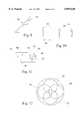
- a CCd camera 40has a plurality of lenses 42 which each receive a subimage of an object 44 illuminated by an outside light source, not shown. The subimage from each lens is focused on a corresponding image sensor 46 which is disposed in a focal plane of its respective lens. Due to the shortened light path between the lenses 42 of FIG. 10 and the corresponding image sensors (e.g. area CCDs), as explained hereinabove, the overall size of the camera may be reduced.
- the lensesmay be disposed in a common plane such that their respective subimages are also focused in a common plane. This, however, may give rise to a relatively large image loss as the area of a circle cannot be fully covered with smaller abutting circles.
- This problemcan partly be solved, as shown in FIGS. 11 and 12 by providing overlapping lenses.
- FIG. 12In the front view of FIG. 12, it can be seen that the circular area corresponding to a single lens of a conventional camera is covered to a substantial decree due to the partial radial overlap of the four lenses. It will be understood, however, that the provision of overlapping lenses as shown in FIGS. 11 and 12 may cause certain image distortions which may require compensating in a known manner.
- image losscan be reduced through the use of wide angle lenses enabling the camera to capture 4 overlapping subimages.
- the use of wide angle lenses for a camera embodiment of the deviceresults in a distortion of each subimage which, when desirable. can be reduced through digital signal processing of the subimages prior to or after reconstruction of the image.
- the use of a wide angle lens in the apparatus of FIGS. 2, 6. 7, or 8reduces the effect of banding and with sufficient light reaching a CCD lens each point on a fingerprint (or other object imaged), an image is reconstructed absent banding. Such an image is reconstructed in dependence upon subimage overlap. Alternatively, such an image is reconstructed in dependence upon a reticle or other indicum. The resulting image is of an object resting on the prism and therefore at a known distance from the lens. This known limitation facilitates image reconstruction and reduction of distortion when desirable.
Landscapes
- Engineering & Computer Science (AREA)
- Theoretical Computer Science (AREA)
- Physics & Mathematics (AREA)
- General Physics & Mathematics (AREA)
- General Engineering & Computer Science (AREA)
- Software Systems (AREA)
- Human Computer Interaction (AREA)
- Computer Security & Cryptography (AREA)
- Optics & Photonics (AREA)
- Multimedia (AREA)
- Computer Hardware Design (AREA)
- Image Input (AREA)
- Measurement Of The Respiration, Hearing Ability, Form, And Blood Characteristics Of Living Organisms (AREA)
Abstract
Description
Claims (19)
Priority Applications (4)
| Application Number | Priority Date | Filing Date | Title |
|---|---|---|---|
| US08/760,212US5859420A (en) | 1996-02-12 | 1996-12-04 | Optical imaging device |
| CA002193041ACA2193041A1 (en) | 1996-02-12 | 1996-12-13 | Mouse adapted to scan biometric data |
| CA002197409ACA2197409A1 (en) | 1996-02-12 | 1997-02-12 | Mouse adapted to scan biometric data |
| US08/797,057US5991431A (en) | 1996-02-12 | 1997-02-12 | Mouse adapted to scan biometric data |
Applications Claiming Priority (2)
| Application Number | Priority Date | Filing Date | Title |
|---|---|---|---|
| US1145996P | 1996-02-12 | 1996-02-12 | |
| US08/760,212US5859420A (en) | 1996-02-12 | 1996-12-04 | Optical imaging device |
Related Child Applications (1)
| Application Number | Title | Priority Date | Filing Date |
|---|---|---|---|
| US08/797,057Continuation-In-PartUS5991431A (en) | 1996-02-12 | 1997-02-12 | Mouse adapted to scan biometric data |
Publications (1)
| Publication Number | Publication Date |
|---|---|
| US5859420Atrue US5859420A (en) | 1999-01-12 |
Family
ID=26682423
Family Applications (2)
| Application Number | Title | Priority Date | Filing Date |
|---|---|---|---|
| US08/760,212Expired - LifetimeUS5859420A (en) | 1996-02-12 | 1996-12-04 | Optical imaging device |
| US08/797,057Expired - LifetimeUS5991431A (en) | 1996-02-12 | 1997-02-12 | Mouse adapted to scan biometric data |
Family Applications After (1)
| Application Number | Title | Priority Date | Filing Date |
|---|---|---|---|
| US08/797,057Expired - LifetimeUS5991431A (en) | 1996-02-12 | 1997-02-12 | Mouse adapted to scan biometric data |
Country Status (2)
| Country | Link |
|---|---|
| US (2) | US5859420A (en) |
| CA (2) | CA2193041A1 (en) |
Cited By (71)
| Publication number | Priority date | Publication date | Assignee | Title |
|---|---|---|---|---|
| US6111977A (en)* | 1997-04-17 | 2000-08-29 | Cross Match Technologies, Inc. | Hand-held fingerprint recognition and transmission device |
| WO2000079215A1 (en)* | 1999-06-23 | 2000-12-28 | Neldon P Johnson | Fingerprint sensing apparatus and method |
| WO2000079214A1 (en)* | 1999-06-23 | 2000-12-28 | Johnson Neldon P | Fingerprint sensing device and method |
| US6178255B1 (en) | 1998-04-28 | 2001-01-23 | Cross Match Technologies, Inc. | Individualized fingerprint scanner |
| US6188781B1 (en)* | 1998-07-28 | 2001-02-13 | Digital Persona, Inc. | Method and apparatus for illuminating a fingerprint through side illumination of a platen |
| US6263090B1 (en) | 1997-05-19 | 2001-07-17 | Cross Match Technologies, Inc. | Code reader fingerprint scanner |
| US6272562B1 (en) | 1999-05-28 | 2001-08-07 | Cross Match Technologies, Inc. | Access control unit interface |
| US6282303B1 (en) | 1998-06-02 | 2001-08-28 | Digital Persona, Inc. | Method and apparatus for scanning a fingerprint using a linear sensor within a cursor control device |
| US6307956B1 (en)* | 1998-04-07 | 2001-10-23 | Gerald R. Black | Writing implement for identity verification system |
| US20010055411A1 (en)* | 2000-05-25 | 2001-12-27 | Black Gerald R. | Identity authentication device |
| US20020025062A1 (en)* | 1998-04-07 | 2002-02-28 | Black Gerald R. | Method for identity verification |
| US6356649B2 (en)* | 1997-04-11 | 2002-03-12 | Arete Associate, Inc. | “Systems and methods with identity verification by streamlined comparison and interpretation of fingerprints and the like” |
| US20020110266A1 (en)* | 1998-11-12 | 2002-08-15 | Teng Harry H. | High contrast, low distortion optical acquisition system for image capturing |
| US20020163601A1 (en)* | 2001-05-04 | 2002-11-07 | Min Kyoung Il | Liquid crystal display and fingerprint capture panel |
| US20030053228A1 (en)* | 2001-09-17 | 2003-03-20 | Lee Jong Ik | Optical fingerprint acquisition apparatus |
| US20030091219A1 (en)* | 1999-08-19 | 2003-05-15 | Martinez Chris J. | Method and apparatus for rolled fingerprint capture |
| US20030123716A1 (en)* | 1999-08-09 | 2003-07-03 | Cross Match Technologies, Inc. | System and method for sending a packet with position address and line scan data over an interface cable |
| US20030128240A1 (en)* | 1999-08-09 | 2003-07-10 | Martinez Chris J. | Method, system, and computer program product for a GUI to fingerprint scanner interface |
| US20030142856A1 (en)* | 2002-01-17 | 2003-07-31 | Cross Match Technology, Inc. | Biometric imaging system and method |
| US20030197593A1 (en)* | 2002-04-19 | 2003-10-23 | Cross Match Technologies, Inc. | Systems and methods utilizing biometric data |
| US20040016811A1 (en)* | 2002-04-19 | 2004-01-29 | Cross Match Technologies, Inc. | Mobile handheld code reader and print scanner system and method |
| US6687391B1 (en) | 1999-10-22 | 2004-02-03 | Cross Match Technologies, Inc. | Adjustable, rotatable finger guide in a tenprint scanner with movable prism platen |
| US6744910B1 (en) | 1999-06-25 | 2004-06-01 | Cross Match Technologies, Inc. | Hand-held fingerprint scanner with on-board image normalization data storage |
| US20040156555A1 (en)* | 1999-08-09 | 2004-08-12 | Cross Match Technologies, Inc. | Calibration and correction in a fingerprint scanner |
| US20040167777A1 (en)* | 2003-02-21 | 2004-08-26 | Hetherington Phillip A. | System for suppressing wind noise |
| US20040165736A1 (en)* | 2003-02-21 | 2004-08-26 | Phil Hetherington | Method and apparatus for suppressing wind noise |
| US20040170303A1 (en)* | 2003-02-28 | 2004-09-02 | Cross Match Technology, Inc. | Dynamic image adaption method for adjusting the quality of digital prints |
| US20050047631A1 (en)* | 2003-08-26 | 2005-03-03 | Cross Match Technologies, Inc. | Method and apparatus for rolled fingerprint image capture with variable blending |
| US6867850B2 (en) | 2002-01-17 | 2005-03-15 | Cross Match Technologies, Inc. | Light wedge for illuminating a platen in a print scanner |
| US6870946B1 (en)* | 1998-08-06 | 2005-03-22 | Secugen Corporation | Compact optical fingerprint capturing and recognition system |
| US20050084142A1 (en)* | 2002-01-18 | 2005-04-21 | Swatton Stewart N.R. | Optical biometric sensor with planar waveguide |
| US6886104B1 (en) | 1999-06-25 | 2005-04-26 | Cross Match Technologies | Rechargeable mobile hand-held fingerprint scanner with a data and power communication interface |
| US6891962B1 (en)* | 1998-09-14 | 2005-05-10 | Mitsubishi Denki Kabushiki Kaisha | Fingerprint sensor and fingerprint recognition system |
| US20050122209A1 (en)* | 2003-12-03 | 2005-06-09 | Black Gerald R. | Security authentication method and system |
| US20050157914A1 (en)* | 2002-08-21 | 2005-07-21 | Jee-Hoon Kim | TFT sensor having improved imaging surface |
| US6928195B2 (en) | 2000-12-18 | 2005-08-09 | Cross Match Technologies, Inc. | Palm scanner using a programmable nutating mirror for increased resolution |
| US20050180618A1 (en)* | 1999-02-10 | 2005-08-18 | Black Gerald R. | Method for identity verification |
| US6944768B2 (en) | 2002-04-19 | 2005-09-13 | Cross Match Technologies, Inc. | System and methods for access control utilizing two factors to control access |
| US6954260B2 (en) | 2002-01-17 | 2005-10-11 | Cross Match Technologies, Inc. | Systems and methods for illuminating a platen in a print scanner |
| US20050231576A1 (en)* | 2001-06-22 | 2005-10-20 | Lee David L | Color reproduction process |
| US20050261972A1 (en)* | 2001-05-25 | 2005-11-24 | Black Gerald R | Pen-based transponder identity verification system |
| US6983062B2 (en) | 2000-08-18 | 2006-01-03 | Cross Match Technologies, Inc. | Fingerprint scanner auto-capture system and method |
| US20060005042A1 (en)* | 1999-09-17 | 2006-01-05 | Black Gerald R | Data security system |
| US20060023922A1 (en)* | 2001-05-25 | 2006-02-02 | Black Gerald R | Identity authentication device |
| US6996259B2 (en) | 2002-08-02 | 2006-02-07 | Cross Match Technologies, Inc. | System and method for counting ridges in a captured print image |
| US20060100868A1 (en)* | 2003-02-21 | 2006-05-11 | Hetherington Phillip A | Minimization of transient noises in a voice signal |
| US20060110015A1 (en)* | 2003-04-04 | 2006-05-25 | Lumidigm, Inc. | Systems and methods for improved biometric feature definition |
| US20060116873A1 (en)* | 2003-02-21 | 2006-06-01 | Harman Becker Automotive Systems - Wavemakers, Inc | Repetitive transient noise removal |
| US20060139778A1 (en)* | 2001-04-26 | 2006-06-29 | Cross Match Technologies, Inc. | Silicone rubber surfaces for biometric print TIR prisms |
| US20060215886A1 (en)* | 2000-01-24 | 2006-09-28 | Black Gerald R | Method for identity verification |
| US7162060B1 (en) | 1999-08-09 | 2007-01-09 | Cross Match Technologies | Method, system, and computer program product for control of platen movement during a live scan |
| US20070078649A1 (en)* | 2003-02-21 | 2007-04-05 | Hetherington Phillip A | Signature noise removal |
| US20070085655A1 (en)* | 2004-02-11 | 2007-04-19 | Wildman Kelvin H | Biometric safe lock |
| US7277562B2 (en) | 2003-08-01 | 2007-10-02 | Cross Match Technologies, Inc. | Biometric imaging capture system and method |
| US20080232653A1 (en)* | 2007-03-21 | 2008-09-25 | Lumidigm, Inc. | Biometrics based on locally consistent features |
| US20080298649A1 (en)* | 2004-06-01 | 2008-12-04 | Lumidigm, Inc. | Hygienic biometric sensors |
| US20090046903A1 (en)* | 2007-04-10 | 2009-02-19 | Lumidigm, Inc. | Biometric Detection Using Spatial, Temporal, And/Or Spectral Techniques |
| US20090080709A1 (en)* | 2006-07-19 | 2009-03-26 | Lumidigm, Inc. | Whole-Hand Multispectral Biometric Imaging |
| US20100067748A1 (en)* | 2004-06-01 | 2010-03-18 | Lumidigm, Inc. | Two camera biometric imaging |
| US20100246902A1 (en)* | 2009-02-26 | 2010-09-30 | Lumidigm, Inc. | Method and apparatus to combine biometric sensing and other functionality |
| US20110085708A1 (en)* | 2009-08-26 | 2011-04-14 | Lumidigm. Inc. | Multiplexed biometric imaging |
| US7949522B2 (en) | 2003-02-21 | 2011-05-24 | Qnx Software Systems Co. | System for suppressing rain noise |
| US20110235872A1 (en)* | 2006-07-19 | 2011-09-29 | Lumidigm, Inc. | Contactless multispectral biometric capture |
| US8184873B2 (en) | 2003-04-04 | 2012-05-22 | Lumidigm, Inc. | White-light spectral biometric sensors |
| US8326621B2 (en) | 2003-02-21 | 2012-12-04 | Qnx Software Systems Limited | Repetitive transient noise removal |
| WO2013022387A1 (en)* | 2011-08-10 | 2013-02-14 | Общество С Ограниченной Ответственностью "Абилма" | Ridge pattern recording system |
| RU2484524C1 (en)* | 2012-05-21 | 2013-06-10 | Общество С Ограниченной Ответственностью "Абилма" | System for recording papillary patterns |
| US8570149B2 (en) | 2010-03-16 | 2013-10-29 | Lumidigm, Inc. | Biometric imaging using an optical adaptive interface |
| US8787630B2 (en) | 2004-08-11 | 2014-07-22 | Lumidigm, Inc. | Multispectral barcode imaging |
| US9042608B2 (en) | 2010-10-25 | 2015-05-26 | Pen-One, Inc. | Data security system |
| US10657354B2 (en) | 2015-01-23 | 2020-05-19 | Abilma LLC | Compact system for registering papillary ridge patterns |
Families Citing this family (95)
| Publication number | Priority date | Publication date | Assignee | Title |
|---|---|---|---|---|
| US10361802B1 (en) | 1999-02-01 | 2019-07-23 | Blanding Hovenweep, Llc | Adaptive pattern recognition based control system and method |
| US7664263B2 (en) | 1998-03-24 | 2010-02-16 | Moskowitz Scott A | Method for combining transfer functions with predetermined key creation |
| US7177429B2 (en) | 2000-12-07 | 2007-02-13 | Blue Spike, Inc. | System and methods for permitting open access to data objects and for securing data within the data objects |
| US7159116B2 (en) | 1999-12-07 | 2007-01-02 | Blue Spike, Inc. | Systems, methods and devices for trusted transactions |
| US6148094A (en)* | 1996-09-30 | 2000-11-14 | David J. Kinsella | Pointing device with biometric sensor |
| US6947580B1 (en) | 1996-09-30 | 2005-09-20 | Dalton Patrick Enterprises, Inc. | Pointing device with biometric sensor |
| US6193153B1 (en)* | 1997-04-16 | 2001-02-27 | Francis Lambert | Method and apparatus for non-intrusive biometric capture |
| CA2208179A1 (en)* | 1997-06-18 | 1998-12-18 | Roland S. Walch | Pointing device with optical fingerprint recognition and tracking capability |
| EP0905646A1 (en)* | 1997-09-30 | 1999-03-31 | Compaq Computer Corporation | Pointing and fingerprint identifier mechanism for a computer system |
| US6408087B1 (en)* | 1998-01-13 | 2002-06-18 | Stmicroelectronics, Inc. | Capacitive semiconductor user input device |
| US6392636B1 (en)* | 1998-01-22 | 2002-05-21 | Stmicroelectronics, Inc. | Touchpad providing screen cursor/pointer movement control |
| US7808479B1 (en) | 2003-09-02 | 2010-10-05 | Apple Inc. | Ambidextrous mouse |
| US6850631B1 (en)* | 1998-02-20 | 2005-02-01 | Oki Electric Industry Co., Ltd. | Photographing device, iris input device and iris image input method |
| DE29804165U1 (en)* | 1998-03-09 | 1998-05-07 | Scm Microsystems Gmbh | Peripheral data communication device |
| JPH11283026A (en)* | 1998-03-26 | 1999-10-15 | Matsushita Electric Ind Co Ltd | Touchpad with fingerprint detection function and information processing device |
| US6906699B1 (en)* | 1998-04-30 | 2005-06-14 | C Technologies Ab | Input unit, method for using the same and input system |
| CA2273560A1 (en)* | 1998-07-17 | 2000-01-17 | David Andrew Inglis | Finger sensor operating technique |
| US6950539B2 (en)* | 1998-09-16 | 2005-09-27 | Digital Persona | Configurable multi-function touchpad device |
| US6415188B1 (en)* | 1998-12-23 | 2002-07-02 | Dennis Sunga Fernandez | Method and apparatus for multi-sensor processing |
| US7664264B2 (en) | 1999-03-24 | 2010-02-16 | Blue Spike, Inc. | Utilizing data reduction in steganographic and cryptographic systems |
| USD433413S (en)* | 1999-04-09 | 2000-11-07 | Biolink Technologies International, Inc. | Biometric scanning aperture for a computer input device |
| AU4714000A (en)* | 1999-05-14 | 2000-12-05 | Biolink Technologies International, Inc. | Biometric system for biometric input, comparison, authentication and access control and method therefor biometric |
| AU4714100A (en)* | 1999-05-14 | 2000-12-05 | Biolink Technologies International, Inc. | Biometric system for biometric input, comparison, authentication and access control and method therefor |
| TW530254B (en)* | 1999-07-08 | 2003-05-01 | Primax Electronics Ltd | Pointing device using grain input device to generate pointing signal |
| US7475246B1 (en) | 1999-08-04 | 2009-01-06 | Blue Spike, Inc. | Secure personal content server |
| JP3679953B2 (en)* | 1999-09-14 | 2005-08-03 | 富士通株式会社 | Personal authentication system using biometric information |
| USD440568S1 (en) | 2000-02-04 | 2001-04-17 | Biolink Technologies International, Inc. | Index finger biometric aperture for a mouse |
| US7587368B2 (en) | 2000-07-06 | 2009-09-08 | David Paul Felsher | Information record infrastructure, system and method |
| US6612928B1 (en) | 2001-02-15 | 2003-09-02 | Sierra Design Group | Player identification using biometric data in a gaming environment |
| US7181017B1 (en) | 2001-03-23 | 2007-02-20 | David Felsher | System and method for secure three-party communications |
| US6914517B2 (en)* | 2001-04-17 | 2005-07-05 | Dalton Patrick Enterprises, Inc. | Fingerprint sensor with feature authentication |
| US7287275B2 (en) | 2002-04-17 | 2007-10-23 | Moskowitz Scott A | Methods, systems and devices for packet watermarking and efficient provisioning of bandwidth |
| US7168047B1 (en)* | 2002-05-28 | 2007-01-23 | Apple Computer, Inc. | Mouse having a button-less panning and scrolling switch |
| US7656393B2 (en) | 2005-03-04 | 2010-02-02 | Apple Inc. | Electronic device having display and surrounding touch sensitive bezel for user interface and control |
| US11275405B2 (en) | 2005-03-04 | 2022-03-15 | Apple Inc. | Multi-functional hand-held device |
| US20040146188A1 (en)* | 2002-08-06 | 2004-07-29 | Carver John F. | Contoured prism print scanners |
| US7358963B2 (en) | 2002-09-09 | 2008-04-15 | Apple Inc. | Mouse having an optically-based scrolling feature |
| US6979264B2 (en)* | 2002-09-12 | 2005-12-27 | Igt | Method and system for verifying entitlement to play a game using biometric identifier |
| US7102617B2 (en)* | 2002-12-30 | 2006-09-05 | Motorola, Inc. | Compact optical pointing apparatus and method |
| US9818136B1 (en) | 2003-02-05 | 2017-11-14 | Steven M. Hoffberg | System and method for determining contingent relevance |
| US8123616B2 (en)* | 2003-03-25 | 2012-02-28 | Igt | Methods and apparatus for limiting access to games using biometric data |
| US7867083B2 (en) | 2003-03-25 | 2011-01-11 | Igt | Methods and apparatus for limiting access to games using biometric data |
| US7245218B2 (en)* | 2003-09-12 | 2007-07-17 | Curtis Satoru Ikehara | Input device to continuously detect biometrics |
| EP1754178A4 (en)* | 2004-01-07 | 2009-07-29 | Identification International I | Low power fingerprint capture system, apparatus, and method |
| US8170945B2 (en)* | 2004-01-15 | 2012-05-01 | Bgc Partners, Inc. | System and method for providing security to a game controller device for electronic trading |
| US7207885B2 (en) | 2004-01-15 | 2007-04-24 | Espeed, Inc. | System and method for using a game controller device for electronic trading |
| JP4705047B2 (en)* | 2004-02-09 | 2011-06-22 | コーニンクレッカ フィリップス エレクトロニクス エヌ ヴィ | Optical input device based on Doppler shift and laser self-mixing |
| US7828652B2 (en) | 2004-02-12 | 2010-11-09 | Igt | Player verification method and system for remote gaming terminals |
| US7637810B2 (en) | 2005-08-09 | 2009-12-29 | Cfph, Llc | System and method for wireless gaming system with alerts |
| US20070060358A1 (en) | 2005-08-10 | 2007-03-15 | Amaitis Lee M | System and method for wireless gaming with location determination |
| US8092303B2 (en) | 2004-02-25 | 2012-01-10 | Cfph, Llc | System and method for convenience gaming |
| US8616967B2 (en) | 2004-02-25 | 2013-12-31 | Cfph, Llc | System and method for convenience gaming |
| US7534169B2 (en) | 2005-07-08 | 2009-05-19 | Cfph, Llc | System and method for wireless gaming system with user profiles |
| KR100594190B1 (en)* | 2004-10-08 | 2006-06-30 | 주식회사 칼라짚미디어 | Removable Mouse |
| US8320645B2 (en)* | 2004-11-02 | 2012-11-27 | Identix Incorporated | High performance multi-mode palmprint and fingerprint scanning device and system |
| US7199868B2 (en)* | 2004-11-02 | 2007-04-03 | Identix Incorporated | High performance fingerprint imaging system |
| AU2005327155B2 (en)* | 2004-11-03 | 2011-03-17 | Pen-One, Inc. | Finger guide device for use with stylus or pen |
| US7929736B2 (en)* | 2004-11-03 | 2011-04-19 | Pen-One, Inc. | Finger guide device for use with stylus or pen |
| US20060093192A1 (en) | 2004-11-03 | 2006-05-04 | Bechtel J S | Finger guide device |
| DE102004053900A1 (en)* | 2004-11-05 | 2006-05-11 | Tbs Holding Ag | Method and device for acquiring biometric data |
| US7710397B2 (en) | 2005-06-03 | 2010-05-04 | Apple Inc. | Mouse with improved input mechanisms using touch sensors |
| DE602005024057D1 (en)* | 2005-06-23 | 2010-11-18 | Nokia Corp | METHOD AND PROGRAM FOR CONTROLLING AN ELECTRONIC EQUIPMENT, ELECTRONIC DEVICE AND SUBSCRIBER APPARATUS |
| US8070604B2 (en) | 2005-08-09 | 2011-12-06 | Cfph, Llc | System and method for providing wireless gaming as a service application |
| US10510214B2 (en) | 2005-07-08 | 2019-12-17 | Cfph, Llc | System and method for peer-to-peer wireless gaming |
| US20070038118A1 (en)* | 2005-08-10 | 2007-02-15 | Depue Marshall Thomas | Subcutaneous tissue imager |
| US7942745B2 (en) | 2005-08-22 | 2011-05-17 | Nintendo Co., Ltd. | Game operating device |
| JP4805633B2 (en) | 2005-08-22 | 2011-11-02 | 任天堂株式会社 | Game operation device |
| US8874477B2 (en) | 2005-10-04 | 2014-10-28 | Steven Mark Hoffberg | Multifactorial optimization system and method |
| CN1987832B (en)* | 2005-12-20 | 2012-03-14 | 鸿富锦精密工业(深圳)有限公司 | Input device with finger print identifying function and its finger print identifying method |
| US8077147B2 (en) | 2005-12-30 | 2011-12-13 | Apple Inc. | Mouse with optical sensing surface |
| US7549576B2 (en) | 2006-05-05 | 2009-06-23 | Cfph, L.L.C. | Systems and methods for providing access to wireless gaming devices |
| US7644861B2 (en) | 2006-04-18 | 2010-01-12 | Bgc Partners, Inc. | Systems and methods for providing access to wireless gaming devices |
| US8939359B2 (en) | 2006-05-05 | 2015-01-27 | Cfph, Llc | Game access device with time varying signal |
| US12136314B2 (en) | 2006-05-05 | 2024-11-05 | Cfph, Llc | Game access device with time varying signal |
| US9306952B2 (en) | 2006-10-26 | 2016-04-05 | Cfph, Llc | System and method for wireless gaming with location determination |
| US8292741B2 (en) | 2006-10-26 | 2012-10-23 | Cfph, Llc | Apparatus, processes and articles for facilitating mobile gaming |
| US9411944B2 (en) | 2006-11-15 | 2016-08-09 | Cfph, Llc | Biometric access sensitivity |
| US8645709B2 (en) | 2006-11-14 | 2014-02-04 | Cfph, Llc | Biometric access data encryption |
| US8510567B2 (en) | 2006-11-14 | 2013-08-13 | Cfph, Llc | Conditional biometric access in a gaming environment |
| US9183693B2 (en) | 2007-03-08 | 2015-11-10 | Cfph, Llc | Game access device |
| US8581721B2 (en) | 2007-03-08 | 2013-11-12 | Cfph, Llc | Game access device with privileges |
| US8319601B2 (en) | 2007-03-14 | 2012-11-27 | Cfph, Llc | Game account access device |
| US20080228618A1 (en) | 2007-03-15 | 2008-09-18 | Noviello Joseph C | System And Method For Providing An Operator Interface For Displaying Market Data, Trader Options, And Trader Input |
| GB0907394D0 (en)* | 2009-04-30 | 2009-06-10 | Antonis Jan | An optical probe |
| US10912991B2 (en)* | 2009-12-09 | 2021-02-09 | Sony Interactive Entertainment LLC | Portable game controller settings |
| US8762734B2 (en)* | 2010-02-10 | 2014-06-24 | Raytheon Company | Biometric pressure grip |
| US8956231B2 (en) | 2010-08-13 | 2015-02-17 | Cfph, Llc | Multi-process communication regarding gaming information |
| US8974302B2 (en) | 2010-08-13 | 2015-03-10 | Cfph, Llc | Multi-process communication regarding gaming information |
| US20220296999A1 (en) | 2010-08-13 | 2022-09-22 | Cfph, Llc | Multi-process communication regarding gaming information |
| TWI621996B (en) | 2015-11-23 | 2018-04-21 | 艾瑞克迪恩 傑森 | Fingerprint reader |
| US10877574B2 (en) | 2017-01-09 | 2020-12-29 | Inventec Appliances (Pudong) Corporation | Computer mouse, touchpad, input suite, and mobile device |
| US12293028B1 (en) | 2017-08-28 | 2025-05-06 | Apple Inc. | Electronic devices with extended input-output capabilities |
| US11449586B2 (en)* | 2018-07-20 | 2022-09-20 | Massachusetts Institute Of Technology | Authenticated intention |
| US10955941B2 (en) | 2019-03-26 | 2021-03-23 | Atlantic Health System, Inc. | Multimodal input device and system for wireless record keeping in a multi-user environment |
| WO2021035583A1 (en)* | 2019-08-28 | 2021-03-04 | 深圳市汇顶科技股份有限公司 | Fingerprint detection apparatus and electronic device |
Citations (4)
| Publication number | Priority date | Publication date | Assignee | Title |
|---|---|---|---|---|
| US3875420A (en)* | 1972-09-25 | 1975-04-01 | Said Bjelkhagen And Said Abram | Device for measurement of the displacement of a tooth |
| US4695716A (en)* | 1985-12-13 | 1987-09-22 | Xerox Corporation | Image sensor array for assembly with like arrays to form a longer array |
| US5432334A (en)* | 1992-11-25 | 1995-07-11 | Xerox Corporation | Method and apparatus for imaging multiple radiation beams |
| US5627363A (en)* | 1995-02-16 | 1997-05-06 | Environmental Research Institute Of Michigan | System and method for three-dimensional imaging of opaque objects using frequency diversity and an opacity constraint |
Family Cites Families (10)
| Publication number | Priority date | Publication date | Assignee | Title |
|---|---|---|---|---|
| US4210899A (en)* | 1975-06-23 | 1980-07-01 | Fingermatrix, Inc. | Fingerprint-based access control and identification apparatus |
| FR2656710A1 (en)* | 1989-12-29 | 1991-07-05 | Radiotechnique Compelec | MICROCONTROLLER FOR THE RAPID EXECUTION OF A LARGE NUMBER OF DECOMPOSABLE OPERATIONS IN THE SEQUENCE OF OPERATIONS OF THE SAME NATURE. |
| GB2244164A (en)* | 1990-05-18 | 1991-11-20 | Philips Electronic Associated | Fingerprint sensing |
| US5229764A (en)* | 1991-06-20 | 1993-07-20 | Matchett Noel D | Continuous biometric authentication matrix |
| US5703356A (en)* | 1992-10-05 | 1997-12-30 | Logitech, Inc. | Pointing device utilizing a photodetector array |
| JP3012138B2 (en)* | 1994-02-04 | 2000-02-21 | 富士通株式会社 | Uneven surface reading device |
| US5546471A (en)* | 1994-10-28 | 1996-08-13 | The National Registry, Inc. | Ergonomic fingerprint reader apparatus |
| US5596454A (en)* | 1994-10-28 | 1997-01-21 | The National Registry, Inc. | Uneven surface image transfer apparatus |
| US5812252A (en)* | 1995-01-31 | 1998-09-22 | Arete Associates | Fingerprint--Acquisition apparatus for access control; personal weapon and other systems controlled thereby |
| US5838306A (en)* | 1995-05-05 | 1998-11-17 | Dell U.S.A., L.P. | Mouse with security feature |
- 1996
- 1996-12-04USUS08/760,212patent/US5859420A/ennot_activeExpired - Lifetime
- 1996-12-13CACA002193041Apatent/CA2193041A1/ennot_activeAbandoned
- 1997
- 1997-02-12USUS08/797,057patent/US5991431A/ennot_activeExpired - Lifetime
- 1997-02-12CACA002197409Apatent/CA2197409A1/ennot_activeAbandoned
Patent Citations (4)
| Publication number | Priority date | Publication date | Assignee | Title |
|---|---|---|---|---|
| US3875420A (en)* | 1972-09-25 | 1975-04-01 | Said Bjelkhagen And Said Abram | Device for measurement of the displacement of a tooth |
| US4695716A (en)* | 1985-12-13 | 1987-09-22 | Xerox Corporation | Image sensor array for assembly with like arrays to form a longer array |
| US5432334A (en)* | 1992-11-25 | 1995-07-11 | Xerox Corporation | Method and apparatus for imaging multiple radiation beams |
| US5627363A (en)* | 1995-02-16 | 1997-05-06 | Environmental Research Institute Of Michigan | System and method for three-dimensional imaging of opaque objects using frequency diversity and an opacity constraint |
Cited By (139)
| Publication number | Priority date | Publication date | Assignee | Title |
|---|---|---|---|---|
| US6356649B2 (en)* | 1997-04-11 | 2002-03-12 | Arete Associate, Inc. | “Systems and methods with identity verification by streamlined comparison and interpretation of fingerprints and the like” |
| US6111977A (en)* | 1997-04-17 | 2000-08-29 | Cross Match Technologies, Inc. | Hand-held fingerprint recognition and transmission device |
| US6263090B1 (en) | 1997-05-19 | 2001-07-17 | Cross Match Technologies, Inc. | Code reader fingerprint scanner |
| US6539101B1 (en)* | 1998-04-07 | 2003-03-25 | Gerald R. Black | Method for identity verification |
| US20050169504A1 (en)* | 1998-04-07 | 2005-08-04 | Black Gerald R. | Method for identity verification |
| US20020025062A1 (en)* | 1998-04-07 | 2002-02-28 | Black Gerald R. | Method for identity verification |
| US7082213B2 (en) | 1998-04-07 | 2006-07-25 | Pen-One Inc. | Method for identity verification |
| US6307956B1 (en)* | 1998-04-07 | 2001-10-23 | Gerald R. Black | Writing implement for identity verification system |
| US20050100196A1 (en)* | 1998-04-28 | 2005-05-12 | Cross Match Technologies Inc. | Methods for capturing fingerprint images using a moving platen |
| US6178255B1 (en) | 1998-04-28 | 2001-01-23 | Cross Match Technologies, Inc. | Individualized fingerprint scanner |
| US6628813B2 (en) | 1998-04-28 | 2003-09-30 | Cross Match Technologies, Inc. | Individualized fingerprint scanner |
| US7103201B2 (en) | 1998-04-28 | 2006-09-05 | Cross Match Technologies, Inc. | Methods for capturing fingerprint images using a moving platen |
| US6282303B1 (en) | 1998-06-02 | 2001-08-28 | Digital Persona, Inc. | Method and apparatus for scanning a fingerprint using a linear sensor within a cursor control device |
| US6324310B1 (en) | 1998-06-02 | 2001-11-27 | Digital Persona, Inc. | Method and apparatus for scanning a fingerprint using a linear sensor |
| US6188781B1 (en)* | 1998-07-28 | 2001-02-13 | Digital Persona, Inc. | Method and apparatus for illuminating a fingerprint through side illumination of a platen |
| US6870946B1 (en)* | 1998-08-06 | 2005-03-22 | Secugen Corporation | Compact optical fingerprint capturing and recognition system |
| US6891962B1 (en)* | 1998-09-14 | 2005-05-10 | Mitsubishi Denki Kabushiki Kaisha | Fingerprint sensor and fingerprint recognition system |
| US20020110266A1 (en)* | 1998-11-12 | 2002-08-15 | Teng Harry H. | High contrast, low distortion optical acquisition system for image capturing |
| US6917695B2 (en) | 1998-11-12 | 2005-07-12 | Secugen Corporation | High contrast, low distortion optical acquisition system for image capturing |
| US20050180618A1 (en)* | 1999-02-10 | 2005-08-18 | Black Gerald R. | Method for identity verification |
| US7961917B2 (en) | 1999-02-10 | 2011-06-14 | Pen-One, Inc. | Method for identity verification |
| US6272562B1 (en) | 1999-05-28 | 2001-08-07 | Cross Match Technologies, Inc. | Access control unit interface |
| US6444969B2 (en) | 1999-06-23 | 2002-09-03 | International Automated Systems, Inc. | Fingerprint sensor and method |
| US6255641B1 (en) | 1999-06-23 | 2001-07-03 | International Automated Systems, Inc. | Fingerprint sensing device and method |
| US6191410B1 (en) | 1999-06-23 | 2001-02-20 | International Automated Systems, Inc | Fingerprint sensing apparatus and method |
| WO2000079214A1 (en)* | 1999-06-23 | 2000-12-28 | Johnson Neldon P | Fingerprint sensing device and method |
| WO2000079215A1 (en)* | 1999-06-23 | 2000-12-28 | Neldon P Johnson | Fingerprint sensing apparatus and method |
| US6886104B1 (en) | 1999-06-25 | 2005-04-26 | Cross Match Technologies | Rechargeable mobile hand-held fingerprint scanner with a data and power communication interface |
| US6744910B1 (en) | 1999-06-25 | 2004-06-01 | Cross Match Technologies, Inc. | Hand-held fingerprint scanner with on-board image normalization data storage |
| US7068822B2 (en) | 1999-08-09 | 2006-06-27 | Cross Match Technologies, Inc. | System and method for sending a packet with position address and line scan data over an interface cable |
| US20040156555A1 (en)* | 1999-08-09 | 2004-08-12 | Cross Match Technologies, Inc. | Calibration and correction in a fingerprint scanner |
| US7010148B2 (en) | 1999-08-09 | 2006-03-07 | Cross Match Technologies, Inc. | Calibration and correction in a fingerprint scanner |
| US7162060B1 (en) | 1999-08-09 | 2007-01-09 | Cross Match Technologies | Method, system, and computer program product for control of platen movement during a live scan |
| US20060239518A1 (en)* | 1999-08-09 | 2006-10-26 | Cross Match Technologies, Inc. | System and method for sending a packet with position address and line scan data over an interface cable |
| US20030123716A1 (en)* | 1999-08-09 | 2003-07-03 | Cross Match Technologies, Inc. | System and method for sending a packet with position address and line scan data over an interface cable |
| US20030128240A1 (en)* | 1999-08-09 | 2003-07-10 | Martinez Chris J. | Method, system, and computer program product for a GUI to fingerprint scanner interface |
| US20030091219A1 (en)* | 1999-08-19 | 2003-05-15 | Martinez Chris J. | Method and apparatus for rolled fingerprint capture |
| US7095880B2 (en) | 1999-08-19 | 2006-08-22 | Cross Match Technologies, Inc. | Method and apparatus for rolled fingerprint capture |
| US7822232B2 (en) | 1999-09-17 | 2010-10-26 | Pen-One, Inc. | Data security system |
| US20060005042A1 (en)* | 1999-09-17 | 2006-01-05 | Black Gerald R | Data security system |
| US8520905B2 (en) | 1999-09-17 | 2013-08-27 | Pen-One, Inc. | Data security system |
| US8374402B2 (en) | 1999-09-17 | 2013-02-12 | Pen-One, Inc. | Data security system |
| US6687391B1 (en) | 1999-10-22 | 2004-02-03 | Cross Match Technologies, Inc. | Adjustable, rotatable finger guide in a tenprint scanner with movable prism platen |
| US7609862B2 (en) | 2000-01-24 | 2009-10-27 | Pen-One Inc. | Method for identity verification |
| US20060215886A1 (en)* | 2000-01-24 | 2006-09-28 | Black Gerald R | Method for identity verification |
| US6970583B2 (en)* | 2000-05-25 | 2005-11-29 | Black Gerald R | Identity authentication device |
| US20010055411A1 (en)* | 2000-05-25 | 2001-12-27 | Black Gerald R. | Identity authentication device |
| US7657067B2 (en) | 2000-08-18 | 2010-02-02 | Cross Match Technologies, Inc. | Fingerprint scanner auto-capture system and method |
| US20060110016A1 (en)* | 2000-08-18 | 2006-05-25 | Cross Match Technologies, Inc. | Fingerprint scanner auto-capture system and method |
| US6983062B2 (en) | 2000-08-18 | 2006-01-03 | Cross Match Technologies, Inc. | Fingerprint scanner auto-capture system and method |
| US6928195B2 (en) | 2000-12-18 | 2005-08-09 | Cross Match Technologies, Inc. | Palm scanner using a programmable nutating mirror for increased resolution |
| US20060139778A1 (en)* | 2001-04-26 | 2006-06-29 | Cross Match Technologies, Inc. | Silicone rubber surfaces for biometric print TIR prisms |
| US7319565B2 (en) | 2001-04-26 | 2008-01-15 | Cross Match Technologies, Inc. | Silicone rubber surfaces for biometric print TIR prisms |
| US20020163601A1 (en)* | 2001-05-04 | 2002-11-07 | Min Kyoung Il | Liquid crystal display and fingerprint capture panel |
| US20050261972A1 (en)* | 2001-05-25 | 2005-11-24 | Black Gerald R | Pen-based transponder identity verification system |
| US20060023922A1 (en)* | 2001-05-25 | 2006-02-02 | Black Gerald R | Identity authentication device |
| US7609863B2 (en) | 2001-05-25 | 2009-10-27 | Pen-One Inc. | Identify authentication device |
| US7281135B2 (en) | 2001-05-25 | 2007-10-09 | Pgn-One Inc. | Pen-based transponder identity verification system |
| US20050231576A1 (en)* | 2001-06-22 | 2005-10-20 | Lee David L | Color reproduction process |
| US20030053228A1 (en)* | 2001-09-17 | 2003-03-20 | Lee Jong Ik | Optical fingerprint acquisition apparatus |
| US6826000B2 (en) | 2001-09-17 | 2004-11-30 | Secugen Corporation | Optical fingerprint acquisition apparatus |
| US7271881B2 (en) | 2002-01-17 | 2007-09-18 | Cross Match Technologies, Inc. | Systems and methods for illuminating a platen in a print scanner |
| US20050180619A1 (en)* | 2002-01-17 | 2005-08-18 | Cross Match Technologies, Inc. | Biometric imaging system and method |
| US7203344B2 (en) | 2002-01-17 | 2007-04-10 | Cross Match Technologies, Inc. | Biometric imaging system and method |
| US7586591B2 (en) | 2002-01-17 | 2009-09-08 | Cross Match Technologies, Inc. | Light wedge for illuminating a platen in a print scanner |
| US20050057742A1 (en)* | 2002-01-17 | 2005-03-17 | Cross Match Technologies, Inc. | Light wedge for illuminating a platen in a print scanner |
| US6867850B2 (en) | 2002-01-17 | 2005-03-15 | Cross Match Technologies, Inc. | Light wedge for illuminating a platen in a print scanner |
| US7308122B2 (en) | 2002-01-17 | 2007-12-11 | Cross Match Technologies, Inc. | Biometric imaging system and method |
| US8073209B2 (en) | 2002-01-17 | 2011-12-06 | Cross Match Technologies, Inc | Biometric imaging system and method |
| US20060170906A1 (en)* | 2002-01-17 | 2006-08-03 | Cross Match Technologies, Inc. | Systems and methods for illuminating a platen in a print scanner |
| US20030142856A1 (en)* | 2002-01-17 | 2003-07-31 | Cross Match Technology, Inc. | Biometric imaging system and method |
| US6954260B2 (en) | 2002-01-17 | 2005-10-11 | Cross Match Technologies, Inc. | Systems and methods for illuminating a platen in a print scanner |
| US20050084142A1 (en)* | 2002-01-18 | 2005-04-21 | Swatton Stewart N.R. | Optical biometric sensor with planar waveguide |
| US7073711B2 (en) | 2002-04-19 | 2006-07-11 | Cross Match Technologies, Inc. | Mobile handheld code reader and print scanner system and method |
| US7079007B2 (en) | 2002-04-19 | 2006-07-18 | Cross Match Technologies, Inc. | Systems and methods utilizing biometric data |
| US20040016811A1 (en)* | 2002-04-19 | 2004-01-29 | Cross Match Technologies, Inc. | Mobile handheld code reader and print scanner system and method |
| US20030197593A1 (en)* | 2002-04-19 | 2003-10-23 | Cross Match Technologies, Inc. | Systems and methods utilizing biometric data |
| US6944768B2 (en) | 2002-04-19 | 2005-09-13 | Cross Match Technologies, Inc. | System and methods for access control utilizing two factors to control access |
| US20050264398A1 (en)* | 2002-04-19 | 2005-12-01 | Cross Match Technologies, Inc. | Systems and methods utilizing biometric data |
| US6996259B2 (en) | 2002-08-02 | 2006-02-07 | Cross Match Technologies, Inc. | System and method for counting ridges in a captured print image |
| US20060133656A1 (en)* | 2002-08-02 | 2006-06-22 | Cross Match Technologies, Inc. | System and method for counting ridges in a captured print image |
| US20050157914A1 (en)* | 2002-08-21 | 2005-07-21 | Jee-Hoon Kim | TFT sensor having improved imaging surface |
| US20110123044A1 (en)* | 2003-02-21 | 2011-05-26 | Qnx Software Systems Co. | Method and Apparatus for Suppressing Wind Noise |
| US20070078649A1 (en)* | 2003-02-21 | 2007-04-05 | Hetherington Phillip A | Signature noise removal |
| US8271279B2 (en) | 2003-02-21 | 2012-09-18 | Qnx Software Systems Limited | Signature noise removal |
| US8374855B2 (en) | 2003-02-21 | 2013-02-12 | Qnx Software Systems Limited | System for suppressing rain noise |
| US9373340B2 (en) | 2003-02-21 | 2016-06-21 | 2236008 Ontario, Inc. | Method and apparatus for suppressing wind noise |
| US8165875B2 (en) | 2003-02-21 | 2012-04-24 | Qnx Software Systems Limited | System for suppressing wind noise |
| US8073689B2 (en) | 2003-02-21 | 2011-12-06 | Qnx Software Systems Co. | Repetitive transient noise removal |
| US20040167777A1 (en)* | 2003-02-21 | 2004-08-26 | Hetherington Phillip A. | System for suppressing wind noise |
| US20060100868A1 (en)* | 2003-02-21 | 2006-05-11 | Hetherington Phillip A | Minimization of transient noises in a voice signal |
| US7885420B2 (en) | 2003-02-21 | 2011-02-08 | Qnx Software Systems Co. | Wind noise suppression system |
| US20040165736A1 (en)* | 2003-02-21 | 2004-08-26 | Phil Hetherington | Method and apparatus for suppressing wind noise |
| US8326621B2 (en) | 2003-02-21 | 2012-12-04 | Qnx Software Systems Limited | Repetitive transient noise removal |
| US7949522B2 (en) | 2003-02-21 | 2011-05-24 | Qnx Software Systems Co. | System for suppressing rain noise |
| US20060116873A1 (en)* | 2003-02-21 | 2006-06-01 | Harman Becker Automotive Systems - Wavemakers, Inc | Repetitive transient noise removal |
| US7725315B2 (en) | 2003-02-21 | 2010-05-25 | Qnx Software Systems (Wavemakers), Inc. | Minimization of transient noises in a voice signal |
| US8612222B2 (en) | 2003-02-21 | 2013-12-17 | Qnx Software Systems Limited | Signature noise removal |
| US7895036B2 (en)* | 2003-02-21 | 2011-02-22 | Qnx Software Systems Co. | System for suppressing wind noise |
| US20110026734A1 (en)* | 2003-02-21 | 2011-02-03 | Qnx Software Systems Co. | System for Suppressing Wind Noise |
| US7164440B2 (en) | 2003-02-28 | 2007-01-16 | Cross Match Technologies, Inc. | Dynamic image adaptation method for adjusting the quality of digital prints |
| US20040170303A1 (en)* | 2003-02-28 | 2004-09-02 | Cross Match Technology, Inc. | Dynamic image adaption method for adjusting the quality of digital prints |
| US20060110015A1 (en)* | 2003-04-04 | 2006-05-25 | Lumidigm, Inc. | Systems and methods for improved biometric feature definition |
| US7627151B2 (en)* | 2003-04-04 | 2009-12-01 | Lumidigm, Inc. | Systems and methods for improved biometric feature definition |
| US8184873B2 (en) | 2003-04-04 | 2012-05-22 | Lumidigm, Inc. | White-light spectral biometric sensors |
| US7277562B2 (en) | 2003-08-01 | 2007-10-02 | Cross Match Technologies, Inc. | Biometric imaging capture system and method |
| US20050047631A1 (en)* | 2003-08-26 | 2005-03-03 | Cross Match Technologies, Inc. | Method and apparatus for rolled fingerprint image capture with variable blending |
| US7363505B2 (en) | 2003-12-03 | 2008-04-22 | Pen-One Inc | Security authentication method and system |
| US20050122209A1 (en)* | 2003-12-03 | 2005-06-09 | Black Gerald R. | Security authentication method and system |
| US20070085655A1 (en)* | 2004-02-11 | 2007-04-19 | Wildman Kelvin H | Biometric safe lock |
| US20080298649A1 (en)* | 2004-06-01 | 2008-12-04 | Lumidigm, Inc. | Hygienic biometric sensors |
| US8165357B2 (en) | 2004-06-01 | 2012-04-24 | Lumidigm, Inc. | Two camera biometric imaging |
| US8913800B2 (en) | 2004-06-01 | 2014-12-16 | Lumidigm, Inc. | Optical biometrics imaging with films |
| US8229185B2 (en) | 2004-06-01 | 2012-07-24 | Lumidigm, Inc. | Hygienic biometric sensors |
| US20100067748A1 (en)* | 2004-06-01 | 2010-03-18 | Lumidigm, Inc. | Two camera biometric imaging |
| US8787630B2 (en) | 2004-08-11 | 2014-07-22 | Lumidigm, Inc. | Multispectral barcode imaging |
| US20110235872A1 (en)* | 2006-07-19 | 2011-09-29 | Lumidigm, Inc. | Contactless multispectral biometric capture |
| US8175346B2 (en) | 2006-07-19 | 2012-05-08 | Lumidigm, Inc. | Whole-hand multispectral biometric imaging |
| US8831297B2 (en) | 2006-07-19 | 2014-09-09 | Lumidigm, Inc. | Contactless multispectral biometric capture |
| US20090080709A1 (en)* | 2006-07-19 | 2009-03-26 | Lumidigm, Inc. | Whole-Hand Multispectral Biometric Imaging |
| US8781181B2 (en) | 2006-07-19 | 2014-07-15 | Lumidigm, Inc. | Contactless multispectral biometric capture |
| US20080232653A1 (en)* | 2007-03-21 | 2008-09-25 | Lumidigm, Inc. | Biometrics based on locally consistent features |
| US8285010B2 (en) | 2007-03-21 | 2012-10-09 | Lumidigm, Inc. | Biometrics based on locally consistent features |
| US8355545B2 (en) | 2007-04-10 | 2013-01-15 | Lumidigm, Inc. | Biometric detection using spatial, temporal, and/or spectral techniques |
| US20090046903A1 (en)* | 2007-04-10 | 2009-02-19 | Lumidigm, Inc. | Biometric Detection Using Spatial, Temporal, And/Or Spectral Techniques |
| US20100246902A1 (en)* | 2009-02-26 | 2010-09-30 | Lumidigm, Inc. | Method and apparatus to combine biometric sensing and other functionality |
| US8872908B2 (en) | 2009-08-26 | 2014-10-28 | Lumidigm, Inc | Dual-imager biometric sensor |
| US8731250B2 (en) | 2009-08-26 | 2014-05-20 | Lumidigm, Inc. | Multiplexed biometric imaging |
| US20110085708A1 (en)* | 2009-08-26 | 2011-04-14 | Lumidigm. Inc. | Multiplexed biometric imaging |
| US20110211055A1 (en)* | 2009-08-26 | 2011-09-01 | Lumidigm, Inc. | Dual-imager biometric sensor |
| US8570149B2 (en) | 2010-03-16 | 2013-10-29 | Lumidigm, Inc. | Biometric imaging using an optical adaptive interface |
| US9042608B2 (en) | 2010-10-25 | 2015-05-26 | Pen-One, Inc. | Data security system |
| RU2475185C1 (en)* | 2011-08-10 | 2013-02-20 | Общество С Ограниченной Ответственностью "Абилма" | Papillary picture recording system |
| WO2013022387A1 (en)* | 2011-08-10 | 2013-02-14 | Общество С Ограниченной Ответственностью "Абилма" | Ridge pattern recording system |
| US9104900B2 (en) | 2011-08-10 | 2015-08-11 | Abilma LLC | Ridge pattern recording system |
| EA023371B1 (en)* | 2011-08-10 | 2016-05-31 | Общество С Ограниченной Ответственностью "Абилма" | Ridge pattern recording system |
| WO2013176573A1 (en)* | 2012-05-21 | 2013-11-28 | Общество С Ограниченной Ответственностью "Абилма" | Papillary ridge pattern registration system |
| RU2484524C1 (en)* | 2012-05-21 | 2013-06-10 | Общество С Ограниченной Ответственностью "Абилма" | System for recording papillary patterns |
| US10657354B2 (en) | 2015-01-23 | 2020-05-19 | Abilma LLC | Compact system for registering papillary ridge patterns |
Also Published As
| Publication number | Publication date |
|---|---|
| US5991431A (en) | 1999-11-23 |
| CA2197409A1 (en) | 1997-08-13 |
| CA2193041A1 (en) | 1997-08-13 |
Similar Documents
| Publication | Publication Date | Title |
|---|---|---|
| US5859420A (en) | Optical imaging device | |
| US6765617B1 (en) | Optoelectronic camera and method for image formatting in the same | |
| US7009652B1 (en) | Image input apparatus | |
| US4467195A (en) | Information detecting apparatus | |
| JPS58225773A (en) | Color image reading method and device | |
| WO2005081020A1 (en) | Optical device and beam splitter | |
| JPH01155308A (en) | Focus detecting device | |
| JP2012065021A (en) | Solid state imaging device | |
| JPH11201819A (en) | Two-dimensional spectral characteristics measuring device | |
| JPS6156914B2 (en) | ||
| EP0377454A3 (en) | Image reading apparatus | |
| JPH06273602A (en) | Contact image sensor | |
| JP2002218510A (en) | 3D image acquisition device | |
| EP3547022A1 (en) | Image capturing device and image capturing method | |
| JPH05100186A (en) | Image sensor | |
| US6281486B1 (en) | Off-axis image correction with spaced photodetectors | |
| TWI861862B (en) | Multispectral optical sensor, camera system and parallax compensation method | |
| TWI822342B (en) | Hyperspectral camera | |
| CN214101550U (en) | Image Sensing Components, Imaging Devices and Terminals | |
| JPH11337815A (en) | Solid-state imaging device and ranging device for camera | |
| JPS5821969A (en) | Color original reader | |
| JP4027994B2 (en) | Imaging device | |
| JPH02243071A (en) | Focusing device for camera | |
| JP2728116B2 (en) | Imaging device | |
| US9020336B1 (en) | Digital streak camera with rotating mirror |
Legal Events
| Date | Code | Title | Description |
|---|---|---|---|
| AS | Assignment | Owner name:DEW ENGINEERING AND DEVELOPMENT LIMITED, CANADA Free format text:ASSIGNMENT OF ASSIGNORS INTEREST;ASSIGNOR:BORZA, STEPHEN J.;REEL/FRAME:008346/0289 Effective date:19961111 | |
| STCF | Information on status: patent grant | Free format text:PATENTED CASE | |
| FEPP | Fee payment procedure | Free format text:PAYOR NUMBER ASSIGNED (ORIGINAL EVENT CODE: ASPN); ENTITY STATUS OF PATENT OWNER: LARGE ENTITY | |
| FEPP | Fee payment procedure | Free format text:PAYER NUMBER DE-ASSIGNED (ORIGINAL EVENT CODE: RMPN); ENTITY STATUS OF PATENT OWNER: LARGE ENTITY Free format text:PAYOR NUMBER ASSIGNED (ORIGINAL EVENT CODE: ASPN); ENTITY STATUS OF PATENT OWNER: LARGE ENTITY | |
| FPAY | Fee payment | Year of fee payment:4 | |
| AS | Assignment | Owner name:ACTIVCARD IRELAND LIMITED, IRELAND Free format text:ASSIGNMENT OF ASSIGNORS INTEREST;ASSIGNOR:DEW ENGINEERING AND DEVELOPMENT LIMITED;REEL/FRAME:013774/0545 Effective date:20030210 | |
| AS | Assignment | Owner name:ACTIVCARD CORP.,CALIFORNIA Free format text:LICENSE AGREEMENT;ASSIGNOR:DISCOBOLUS MANAGEMENT, LLC;REEL/FRAME:016547/0216 Effective date:20050606 Owner name:ACTIVCARD CORP., CALIFORNIA Free format text:LICENSE AGREEMENT;ASSIGNOR:DISCOBOLUS MANAGEMENT, LLC;REEL/FRAME:016547/0216 Effective date:20050606 | |
| FEPP | Fee payment procedure | Free format text:PAT HOLDER NO LONGER CLAIMS SMALL ENTITY STATUS, ENTITY STATUS SET TO UNDISCOUNTED (ORIGINAL EVENT CODE: STOL); ENTITY STATUS OF PATENT OWNER: LARGE ENTITY | |
| REFU | Refund | Free format text:REFUND - PAYMENT OF MAINTENANCE FEE, 8TH YR, SMALL ENTITY (ORIGINAL EVENT CODE: R2552); ENTITY STATUS OF PATENT OWNER: LARGE ENTITY | |
| FPAY | Fee payment | Year of fee payment:8 | |
| FEPP | Fee payment procedure | Free format text:ENTITY STATUS SET TO UNDISCOUNTED (ORIGINAL EVENT CODE: BIG.); ENTITY STATUS OF PATENT OWNER: LARGE ENTITY | |
| FEPP | Fee payment procedure | Free format text:PAYER NUMBER DE-ASSIGNED (ORIGINAL EVENT CODE: RMPN); ENTITY STATUS OF PATENT OWNER: LARGE ENTITY Free format text:PAYOR NUMBER ASSIGNED (ORIGINAL EVENT CODE: ASPN); ENTITY STATUS OF PATENT OWNER: LARGE ENTITY | |
| FPAY | Fee payment | Year of fee payment:12 |