US5858825A - Methods for reducing anomalous narrow channel effect in trench-bounded buried-channel p-MOSFETS - Google Patents
Methods for reducing anomalous narrow channel effect in trench-bounded buried-channel p-MOSFETSDownload PDFInfo
- Publication number
- US5858825A US5858825AUS08/893,053US89305397AUS5858825AUS 5858825 AUS5858825 AUS 5858825AUS 89305397 AUS89305397 AUS 89305397AUS 5858825 AUS5858825 AUS 5858825A
- Authority
- US
- United States
- Prior art keywords
- channel
- buried
- method recited
- boron
- low temperature
- Prior art date
- Legal status (The legal status is an assumption and is not a legal conclusion. Google has not performed a legal analysis and makes no representation as to the accuracy of the status listed.)
- Expired - Lifetime
Links
- 238000000034methodMethods0.000titleclaimsabstractdescription38
- 230000002547anomalous effectEffects0.000titleclaimsabstractdescription18
- 230000000694effectsEffects0.000titleclaimsdescription14
- 229910052796boronInorganic materials0.000claimsabstractdescription42
- ZOXJGFHDIHLPTG-UHFFFAOYSA-NBoronChemical compound[B]ZOXJGFHDIHLPTG-UHFFFAOYSA-N0.000claimsabstractdescription35
- 230000003647oxidationEffects0.000claimsabstractdescription30
- 238000007254oxidation reactionMethods0.000claimsabstractdescription30
- 238000000137annealingMethods0.000claimsabstractdescription13
- BHEPBYXIRTUNPN-UHFFFAOYSA-Nhydridophosphorus(.) (triplet)Chemical compound[PH]BHEPBYXIRTUNPN-UHFFFAOYSA-N0.000claimsabstractdescription13
- 230000000977initiatory effectEffects0.000claimsabstractdescription8
- 239000011261inert gasSubstances0.000claimsabstractdescription7
- 239000004065semiconductorSubstances0.000claimsabstractdescription5
- 238000004519manufacturing processMethods0.000claimsabstractdescription3
- 238000002955isolationMethods0.000claimsdescription11
- XKRFYHLGVUSROY-UHFFFAOYSA-NArgonChemical compound[Ar]XKRFYHLGVUSROY-UHFFFAOYSA-N0.000claimsdescription10
- IJGRMHOSHXDMSA-UHFFFAOYSA-NAtomic nitrogenChemical compoundN#NIJGRMHOSHXDMSA-UHFFFAOYSA-N0.000claimsdescription10
- -1phosphorous ionsChemical class0.000claimsdescription9
- 229910052786argonInorganic materials0.000claimsdescription5
- 229910052757nitrogenInorganic materials0.000claimsdescription5
- 230000001629suppressionEffects0.000claimsdescription4
- 239000000758substrateSubstances0.000claims5
- 238000002513implantationMethods0.000claims2
- 239000007943implantSubstances0.000abstractdescription14
- 238000005516engineering processMethods0.000abstractdescription4
- 230000035945sensitivityEffects0.000abstractdescription3
- 230000005669field effectEffects0.000abstractdescription2
- 229910044991metal oxideInorganic materials0.000abstractdescription2
- 150000004706metal oxidesChemical class0.000abstractdescription2
- 230000008569processEffects0.000description13
- 238000009792diffusion processMethods0.000description6
- 230000003247decreasing effectEffects0.000description5
- 230000009467reductionEffects0.000description4
- OAICVXFJPJFONN-UHFFFAOYSA-NPhosphorusChemical compound[P]OAICVXFJPJFONN-UHFFFAOYSA-N0.000description3
- 238000009826distributionMethods0.000description3
- 229910052698phosphorusInorganic materials0.000description3
- 239000011574phosphorusSubstances0.000description3
- 238000005215recombinationMethods0.000description3
- 230000006798recombinationEffects0.000description3
- 230000001052transient effectEffects0.000description3
- VYPSYNLAJGMNEJ-UHFFFAOYSA-NSilicium dioxideChemical compoundO=[Si]=OVYPSYNLAJGMNEJ-UHFFFAOYSA-N0.000description2
- XUIMIQQOPSSXEZ-UHFFFAOYSA-NSiliconChemical compound[Si]XUIMIQQOPSSXEZ-UHFFFAOYSA-N0.000description2
- 230000007423decreaseEffects0.000description2
- 239000002019doping agentSubstances0.000description2
- 230000004907fluxEffects0.000description2
- 229910052710siliconInorganic materials0.000description2
- 239000010703siliconSubstances0.000description2
- 239000000243solutionSubstances0.000description2
- 239000000969carrierSubstances0.000description1
- 229910052681coesiteInorganic materials0.000description1
- 230000001010compromised effectEffects0.000description1
- 238000011960computer-aided designMethods0.000description1
- 229910052906cristobaliteInorganic materials0.000description1
- 230000007547defectEffects0.000description1
- 230000001419dependent effectEffects0.000description1
- 238000002347injectionMethods0.000description1
- 239000007924injectionSubstances0.000description1
- 230000010354integrationEffects0.000description1
- 238000005468ion implantationMethods0.000description1
- 230000004048modificationEffects0.000description1
- 238000012986modificationMethods0.000description1
- 230000001590oxidative effectEffects0.000description1
- 238000005204segregationMethods0.000description1
- 239000000377silicon dioxideSubstances0.000description1
- 238000004088simulationMethods0.000description1
- 229910052682stishoviteInorganic materials0.000description1
- 229910052905tridymiteInorganic materials0.000description1
Images


Classifications
- H—ELECTRICITY
- H10—SEMICONDUCTOR DEVICES; ELECTRIC SOLID-STATE DEVICES NOT OTHERWISE PROVIDED FOR
- H10B—ELECTRONIC MEMORY DEVICES
- H10B12/00—Dynamic random access memory [DRAM] devices
- H10B12/01—Manufacture or treatment
- H10B12/02—Manufacture or treatment for one transistor one-capacitor [1T-1C] memory cells
- H10B12/05—Making the transistor
- H—ELECTRICITY
- H10—SEMICONDUCTOR DEVICES; ELECTRIC SOLID-STATE DEVICES NOT OTHERWISE PROVIDED FOR
- H10D—INORGANIC ELECTRIC SEMICONDUCTOR DEVICES
- H10D30/00—Field-effect transistors [FET]
- H10D30/60—Insulated-gate field-effect transistors [IGFET]
- H10D30/637—Lateral IGFETs having no inversion channels, e.g. buried channel lateral IGFETs, normally-on lateral IGFETs or depletion-mode lateral IGFETs
- H—ELECTRICITY
- H10—SEMICONDUCTOR DEVICES; ELECTRIC SOLID-STATE DEVICES NOT OTHERWISE PROVIDED FOR
- H10D—INORGANIC ELECTRIC SEMICONDUCTOR DEVICES
- H10D62/00—Semiconductor bodies, or regions thereof, of devices having potential barriers
- H10D62/10—Shapes, relative sizes or dispositions of the regions of the semiconductor bodies; Shapes of the semiconductor bodies
- H10D62/113—Isolations within a component, i.e. internal isolations
- H—ELECTRICITY
- H10—SEMICONDUCTOR DEVICES; ELECTRIC SOLID-STATE DEVICES NOT OTHERWISE PROVIDED FOR
- H10D—INORGANIC ELECTRIC SEMICONDUCTOR DEVICES
- H10D62/00—Semiconductor bodies, or regions thereof, of devices having potential barriers
- H10D62/10—Shapes, relative sizes or dispositions of the regions of the semiconductor bodies; Shapes of the semiconductor bodies
- H10D62/17—Semiconductor regions connected to electrodes not carrying current to be rectified, amplified or switched, e.g. channel regions
- H10D62/213—Channel regions of field-effect devices
- H10D62/221—Channel regions of field-effect devices of FETs
- H10D62/235—Channel regions of field-effect devices of FETs of IGFETs
- H—ELECTRICITY
- H10—SEMICONDUCTOR DEVICES; ELECTRIC SOLID-STATE DEVICES NOT OTHERWISE PROVIDED FOR
- H10D—INORGANIC ELECTRIC SEMICONDUCTOR DEVICES
- H10D62/00—Semiconductor bodies, or regions thereof, of devices having potential barriers
- H10D62/10—Shapes, relative sizes or dispositions of the regions of the semiconductor bodies; Shapes of the semiconductor bodies
- H10D62/17—Semiconductor regions connected to electrodes not carrying current to be rectified, amplified or switched, e.g. channel regions
- H10D62/393—Body regions of DMOS transistors or IGBTs
- H—ELECTRICITY
- H10—SEMICONDUCTOR DEVICES; ELECTRIC SOLID-STATE DEVICES NOT OTHERWISE PROVIDED FOR
- H10D—INORGANIC ELECTRIC SEMICONDUCTOR DEVICES
- H10D84/00—Integrated devices formed in or on semiconductor substrates that comprise only semiconducting layers, e.g. on Si wafers or on GaAs-on-Si wafers
- H10D84/01—Manufacture or treatment
- H10D84/0123—Integrating together multiple components covered by H10D12/00 or H10D30/00, e.g. integrating multiple IGBTs
- H10D84/0126—Integrating together multiple components covered by H10D12/00 or H10D30/00, e.g. integrating multiple IGBTs the components including insulated gates, e.g. IGFETs
- H10D84/0128—Manufacturing their channels
- H—ELECTRICITY
- H10—SEMICONDUCTOR DEVICES; ELECTRIC SOLID-STATE DEVICES NOT OTHERWISE PROVIDED FOR
- H10D—INORGANIC ELECTRIC SEMICONDUCTOR DEVICES
- H10D84/00—Integrated devices formed in or on semiconductor substrates that comprise only semiconducting layers, e.g. on Si wafers or on GaAs-on-Si wafers
- H10D84/01—Manufacture or treatment
- H10D84/02—Manufacture or treatment characterised by using material-based technologies
- H10D84/03—Manufacture or treatment characterised by using material-based technologies using Group IV technology, e.g. silicon technology or silicon-carbide [SiC] technology
- H10D84/038—Manufacture or treatment characterised by using material-based technologies using Group IV technology, e.g. silicon technology or silicon-carbide [SiC] technology using silicon technology, e.g. SiGe
- H—ELECTRICITY
- H10—SEMICONDUCTOR DEVICES; ELECTRIC SOLID-STATE DEVICES NOT OTHERWISE PROVIDED FOR
- H10D—INORGANIC ELECTRIC SEMICONDUCTOR DEVICES
- H10D84/00—Integrated devices formed in or on semiconductor substrates that comprise only semiconducting layers, e.g. on Si wafers or on GaAs-on-Si wafers
- H10D84/80—Integrated devices formed in or on semiconductor substrates that comprise only semiconducting layers, e.g. on Si wafers or on GaAs-on-Si wafers characterised by the integration of at least one component covered by groups H10D12/00 or H10D30/00, e.g. integration of IGFETs
- H10D84/82—Integrated devices formed in or on semiconductor substrates that comprise only semiconducting layers, e.g. on Si wafers or on GaAs-on-Si wafers characterised by the integration of at least one component covered by groups H10D12/00 or H10D30/00, e.g. integration of IGFETs of only field-effect components
- H10D84/83—Integrated devices formed in or on semiconductor substrates that comprise only semiconducting layers, e.g. on Si wafers or on GaAs-on-Si wafers characterised by the integration of at least one component covered by groups H10D12/00 or H10D30/00, e.g. integration of IGFETs of only field-effect components of only insulated-gate FETs [IGFET]
- H10D84/85—Complementary IGFETs, e.g. CMOS
- H10D84/854—Complementary IGFETs, e.g. CMOS comprising arrangements for preventing bipolar actions between the different IGFET regions, e.g. arrangements for latchup prevention
Definitions
- the present inventiongenerally relates to methods of manufacture of trench-bounded buried-channel p-type metal oxide semiconductor field effect transistors (p-MOSFETs) as used in dynamic random access memory (DRAM) technologies and, more particularly, to methods for significantly reducing the anomalous buried-channel p-MOSFET sensitivity to device width.
- p-MOSFETstrench-bounded buried-channel p-type metal oxide semiconductor field effect transistors
- DRAMdynamic random access memory
- inverse narrow channel effectwhen the standard current definition of threshold voltage, ##EQU1## is applied, where W des and L des are the design width and design length of the device, respectively.
- W des and L desare the design width and design length of the device, respectively.
- V tdefined by the above equation, inverse narrow channel effect is characterized by a decrease in the magnitude of V t as the width of the device decreases.
- the performance of the widest devicesis compromised as a result of the higher than desired V t . Consequently, to assure that the narrowest devices meet the off-current objective, the magnitude of the V t of the widest devices must be set higher than required by the off-current objective. This results in a performance penalty for the wider devices of typically a 100 mV loss of overdrive.
- a method for eliminating the anomalous channel effectincluding the steps of implanting at least one deep phosphorous n-well; initiating a low temperature anneal using an inert gas; implanting a boron buried-channel; and initiating a gate oxidation.
- the low temperature annealing stepis performed at about 750° C. to about 800° C., for a period of about 10 minutes to about 120 minutes, and utilizes an inert gas, such as, for example, nitrogen or argon.
- the low temperature annealmay be performed after implanting the boron buried-channel and prior to initiating the gate oxidation.
- a method for eliminating the anomalous channel effectincluding the steps of implanting at least one deep phosphorous n-well; implanting a boron buried-channel; and initiating a rapid thermal oxidation (RTO) gate oxidation step.
- the RTOis performed at about 1025° C. to about 1075° C. for a period of time sufficient to grow the gate oxide.
- the RTO stepmay be followed by a standard gate oxidation step performed at about 850° C.
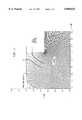
- FIG. 1is a graph superimposed on a cross-section of a portion of an oxide trench isolation showing interstitial (excess) contours at the beginning of an 850° C. gate oxidation step using process recipe "A";
- FIG. 2is a cross-section similar to FIG. 1 showing the boron buried layer puddle responsible for anomalous V t dependence on channel width using process recipe "A";
- FIG. 3is a graph showing measured and modeled V t versus width (W) for process recipe "A" demonstrating the anomalous Vt dependence on width down to ⁇ 0.4 ⁇ m;
- FIG. 4is a graph showing the effect on the anomalous narrow channel behavior of the solution using process recipe "B" according to the invention.
- FIG. 5is a graph showing the effect on the anomalous narrow channel behavior of the solution using process recipe "C" according to the invention.
- the excess interstitial concentration and, hence, the boron diffusivityincrease and the boron distribution broadens.
- the minimum in the peak net p-type concentration of the buried layeroccurs at mid-width and is accentuated by the compensation of boron by the n-well doping.
- the gradient in the excess interstitial concentrationdrives the boron towards the trench edge.
- segregation induced boron depletion and n-type dopant pile-upreduce the net p-type concentration.
- the overall effect of the excess interstitial distribution on the diffusion of boron during the 850° C. gate oxidation stepis the creation of a "boron puddle" 100 near the trench edge, as shown by the simulated net doping distribution at the end of the process in FIG. 2.
- Modelingshows that the peak net p-type concentration in the "boron puddle" is approximately 32% greater than at mid-width, for a 2 ⁇ m wide device. As the device width is reduced down to approximately 0.4 ⁇ m, the peak net p-type concentration increases because of decreased interstitial concentration at the top surface resulting from recombination on the trench sidewall.
- FIG. 3shows measured V t versus W (width) characteristics compared with simulated results. As illustrated in FIG. 3, the magnitude of V t drops by approximately 150 mV when the device width is reduced from 2 ⁇ m to 0.4 ⁇ m. This results in a loss of overdrive of approximately 100 mV for the widest channel p-FETS used in a design.
- part of the present process for making trench-bounded buried-channel p-MOSFETScomprising the following steps: (1) implanting at least one deep phosphorus n-well; (2) implanting a boron buried-channel; and (3) initiating a 850° C. dry gate oxidation step--results in an anomalous narrow channel behavior.
- the anomalous narrow channel behaviorcan be achieved by implementing a low temperature annealing step, utilizing an inert gas, immediately following the deep phosphorus implant and prior to the boron buried-channel implant.
- the low temperature annealing stepmay be initiated after the boron buried-channel implant and prior to the 850° C. dry gate oxidation step.
- the low temperature anneal(referred to as process recipe "B") may be performed at a temperature of between about 750° C. to about 800° C. Temperatures much above 800° C. are undesirable as this will increase phosphorous diffusion. Temperatures much below 750° C. result in reduced interstitial recombination. Regarding the duration of the annealing step, a reduction of the anomalous narrow channel behavior has been observed for periods ranging from about 10 minutes to about 120 minutes.
- the low temperature annealis carried out with an inert gas, such as, by way of example and not by limitation, nitrogen or argon.
- FIG. 4compares the simulated and measured V t vs. W characteristics for devices fabricated using recipe "B” with simulated behavior using recipe "A".
- Recipe “B”includes a low temperature anneal at 800° C. for about 60 minutes prior to gate oxidation at 850° C.
- the threshold voltage V tremains nearly constant as the device width is reduced from about 2 ⁇ m to about 0.4 ⁇ m.
- the net p-type concentrationpeaks only 3% above mid-width value for a device width of 2 ⁇ m.
- the normal narrow channel behavior--increased magnitude of V t with decreasing W--is observed at device widths below about 0.4 ⁇ m.
- RTOrapid thermal oxidation
- A850° C. gate oxidation step
- Cprocess recipe
- the duration of the RTO gate oxidation stepis dependent upon the desired thickness of the gate oxide. For example, for a gate oxide thickness of 80 angstroms, the duration of the RTO gate oxidation step would be about 1.3 minutes.
- the twocan be used in conjunction, with the duration of the RTO step being reduced somewhat to be followed by the 850° C. gate oxidation step.
- FIG. 5compares the simulated V t vs. W characteristics for devices fabricated using recipe "C” with simulated behavior using recipe "A". As shown in FIG. 5, the threshold voltage V t remains nearly constant as the device width is reduced from about 21 ⁇ m to about 0.4 ⁇ m. The normal narrow channel behavior is observed at device widths below about 0.4 ⁇ m. Simulation shows the magnitude of the "boron puddle” and the anomalous V t width dependence are negligible for this process.
Landscapes
- Engineering & Computer Science (AREA)
- Manufacturing & Machinery (AREA)
- Insulated Gate Type Field-Effect Transistor (AREA)
- Semiconductor Memories (AREA)
Abstract
Description
Claims (16)
Priority Applications (1)
| Application Number | Priority Date | Filing Date | Title |
|---|---|---|---|
| US08/893,053US5858825A (en) | 1994-06-30 | 1997-07-14 | Methods for reducing anomalous narrow channel effect in trench-bounded buried-channel p-MOSFETS |
Applications Claiming Priority (3)
| Application Number | Priority Date | Filing Date | Title |
|---|---|---|---|
| US08/269,857US5559050A (en) | 1994-06-30 | 1994-06-30 | P-MOSFETS with enhanced anomalous narrow channel effect |
| US35192494A | 1994-12-08 | 1994-12-08 | |
| US08/893,053US5858825A (en) | 1994-06-30 | 1997-07-14 | Methods for reducing anomalous narrow channel effect in trench-bounded buried-channel p-MOSFETS |
Related Parent Applications (1)
| Application Number | Title | Priority Date | Filing Date |
|---|---|---|---|
| US35192494AContinuation | 1994-06-30 | 1994-12-08 |
Publications (1)
| Publication Number | Publication Date |
|---|---|
| US5858825Atrue US5858825A (en) | 1999-01-12 |
Family
ID=26953945
Family Applications (2)
| Application Number | Title | Priority Date | Filing Date |
|---|---|---|---|
| US08/625,962Expired - Fee RelatedUS6271093B1 (en) | 1994-06-30 | 1996-04-01 | Methods for reducing anomalous narrow channel effect in trench-bounded buried-channel p-MOSFETs |
| US08/893,053Expired - LifetimeUS5858825A (en) | 1994-06-30 | 1997-07-14 | Methods for reducing anomalous narrow channel effect in trench-bounded buried-channel p-MOSFETS |
Family Applications Before (1)
| Application Number | Title | Priority Date | Filing Date |
|---|---|---|---|
| US08/625,962Expired - Fee RelatedUS6271093B1 (en) | 1994-06-30 | 1996-04-01 | Methods for reducing anomalous narrow channel effect in trench-bounded buried-channel p-MOSFETs |
Country Status (1)
| Country | Link |
|---|---|
| US (2) | US6271093B1 (en) |
Cited By (7)
| Publication number | Priority date | Publication date | Assignee | Title |
|---|---|---|---|---|
| US6081662A (en)* | 1996-05-27 | 2000-06-27 | Mitsubishi Denki Kabushiki Kaisha | Semiconductor device including trench isolation structure and a method of manufacturing thereof |
| US20030033043A1 (en)* | 2001-08-13 | 2003-02-13 | Promos Technologies | Method to reduce lot-to-lot variation of array threshold voltage in a DRAM device |
| US6743688B1 (en)* | 1998-01-05 | 2004-06-01 | Advanced Micro Devices, Inc. | High performance MOSFET with modulated channel gate thickness |
| US20050181565A1 (en)* | 2003-10-20 | 2005-08-18 | Ethan Williford | Threshold voltage adjustment for long channel transistors |
| US20050277271A1 (en)* | 2004-06-09 | 2005-12-15 | International Business Machines Corporation | RAISED STI PROCESS FOR MULTIPLE GATE OX AND SIDEWALL PROTECTION ON STRAINED Si/SGOI STRUCTURE WITH ELEVATED SOURCE/DRAIN |
| US8466496B2 (en) | 2011-11-17 | 2013-06-18 | International Business Machines Corporation | Selective partial gate stack for improved device isolation |
| US8779469B2 (en) | 2011-10-20 | 2014-07-15 | International Business Machines Corporation | Post-gate shallow trench isolation structure formation |
Citations (24)
| Publication number | Priority date | Publication date | Assignee | Title |
|---|---|---|---|---|
| US4181538A (en)* | 1978-09-26 | 1980-01-01 | The United States Of America As Represented By The United States Department Of Energy | Method for making defect-free zone by laser-annealing of doped silicon |
| US4230505A (en)* | 1979-10-09 | 1980-10-28 | Rca Corporation | Method of making an impatt diode utilizing a combination of epitaxial deposition, ion implantation and substrate removal |
| US4234355A (en)* | 1977-12-13 | 1980-11-18 | Robert Bosch Gmbh | Method for manufacturing a semiconductor element utilizing thermal neutron irradiation and annealing |
| US4242791A (en)* | 1979-09-21 | 1981-01-06 | International Business Machines Corporation | High performance bipolar transistors fabricated by post emitter base implantation process |
| US4349395A (en)* | 1978-03-25 | 1982-09-14 | Fujitsu Limited | Method for producing MOS semiconductor device |
| US4477310A (en)* | 1983-08-12 | 1984-10-16 | Tektronix, Inc. | Process for manufacturing MOS integrated circuit with improved method of forming refractory metal silicide areas |
| US4486266A (en)* | 1983-08-12 | 1984-12-04 | Tektronix, Inc. | Integrated circuit method |
| US4554726A (en)* | 1984-04-17 | 1985-11-26 | At&T Bell Laboratories | CMOS Integrated circuit technology utilizing dual implantation of slow and fast diffusing donor ions to form the n-well |
| US4651411A (en)* | 1981-10-27 | 1987-03-24 | Tokyo Shibaura Denki Kabushiki Kaisha | Method of manufacturing a MOS device wherein an insulating film is deposited in a field region |
| US4732874A (en)* | 1986-10-15 | 1988-03-22 | Delco Electronics Corporation | Removing metal precipitates from semiconductor devices |
| US4784975A (en)* | 1986-10-23 | 1988-11-15 | International Business Machines Corporation | Post-oxidation anneal of silicon dioxide |
| US4833096A (en)* | 1988-01-19 | 1989-05-23 | Atmel Corporation | EEPROM fabrication process |
| US4877751A (en)* | 1988-03-11 | 1989-10-31 | National Semiconductor Corporation | Method of forming an N+ poly-to- N+ silicon capacitor structure utilizing a deep phosphorous implant |
| US5015593A (en)* | 1989-05-15 | 1991-05-14 | Kabushiki Kaisha Toshiba | Method of manufacturing semiconductor device |
| US5023193A (en)* | 1986-07-16 | 1991-06-11 | National Semiconductor Corp. | Method for simultaneously fabricating bipolar and complementary field effect transistors using a minimal number of masks |
| US5169796A (en)* | 1991-09-19 | 1992-12-08 | Teledyne Industries, Inc. | Process for fabricating self-aligned metal gate field effect transistors |
| US5192708A (en)* | 1991-04-29 | 1993-03-09 | International Business Machines Corporation | Sub-layer contact technique using in situ doped amorphous silicon and solid phase recrystallization |
| US5219767A (en)* | 1990-08-22 | 1993-06-15 | Nec Corporation | Process for preparing semiconductor device |
| US5314848A (en)* | 1990-09-25 | 1994-05-24 | Matsushita Electric Industrial Co., Ltd. | Method for manufacturing a semiconductor device using a heat treatment according to a temperature profile that prevents grain or particle precipitation during reflow |
| US5338694A (en)* | 1990-04-02 | 1994-08-16 | National Semiconductor Corporation | Method of fabricating BiCMOS device |
| US5384279A (en)* | 1988-09-09 | 1995-01-24 | U.S. Philips Corporation | Method of manufacturing a semiconductor device comprising a silicon body in which semiconductor regions are formed by ion implantations |
| US5387552A (en)* | 1991-03-22 | 1995-02-07 | National Semiconductor Corporation | Method of fabrication of PNP structure in a common substrate containing NPN or MOS structures |
| US5413944A (en)* | 1994-05-06 | 1995-05-09 | United Microelectronics Corporation | Twin tub CMOS process |
| US5559050A (en)* | 1994-06-30 | 1996-09-24 | International Business Machines Corporation | P-MOSFETS with enhanced anomalous narrow channel effect |
Family Cites Families (4)
| Publication number | Priority date | Publication date | Assignee | Title |
|---|---|---|---|---|
| US5024962A (en)* | 1990-04-20 | 1991-06-18 | Teledyne Industries, Inc. | Method for preventing auto-doping in the fabrication of metal gate CMOS devices |
| US5091324A (en)* | 1990-08-10 | 1992-02-25 | Advanced Micro Devices, Inc. | Process for producing optimum intrinsic, long channel, and short channel mos devices in vlsi structures |
| EP0562207B1 (en)* | 1992-03-27 | 1996-06-05 | International Business Machines Corporation | Method of forming thin film pseudo-planar PFET devices and structures resulting therefrom |
| US5294571A (en)* | 1992-07-22 | 1994-03-15 | Vlsi Technology, Inc. | Rapid thermal oxidation of silicon in an ozone ambient |
- 1996
- 1996-04-01USUS08/625,962patent/US6271093B1/ennot_activeExpired - Fee Related
- 1997
- 1997-07-14USUS08/893,053patent/US5858825A/ennot_activeExpired - Lifetime
Patent Citations (24)
| Publication number | Priority date | Publication date | Assignee | Title |
|---|---|---|---|---|
| US4234355A (en)* | 1977-12-13 | 1980-11-18 | Robert Bosch Gmbh | Method for manufacturing a semiconductor element utilizing thermal neutron irradiation and annealing |
| US4349395A (en)* | 1978-03-25 | 1982-09-14 | Fujitsu Limited | Method for producing MOS semiconductor device |
| US4181538A (en)* | 1978-09-26 | 1980-01-01 | The United States Of America As Represented By The United States Department Of Energy | Method for making defect-free zone by laser-annealing of doped silicon |
| US4242791A (en)* | 1979-09-21 | 1981-01-06 | International Business Machines Corporation | High performance bipolar transistors fabricated by post emitter base implantation process |
| US4230505A (en)* | 1979-10-09 | 1980-10-28 | Rca Corporation | Method of making an impatt diode utilizing a combination of epitaxial deposition, ion implantation and substrate removal |
| US4651411A (en)* | 1981-10-27 | 1987-03-24 | Tokyo Shibaura Denki Kabushiki Kaisha | Method of manufacturing a MOS device wherein an insulating film is deposited in a field region |
| US4486266A (en)* | 1983-08-12 | 1984-12-04 | Tektronix, Inc. | Integrated circuit method |
| US4477310A (en)* | 1983-08-12 | 1984-10-16 | Tektronix, Inc. | Process for manufacturing MOS integrated circuit with improved method of forming refractory metal silicide areas |
| US4554726A (en)* | 1984-04-17 | 1985-11-26 | At&T Bell Laboratories | CMOS Integrated circuit technology utilizing dual implantation of slow and fast diffusing donor ions to form the n-well |
| US5023193A (en)* | 1986-07-16 | 1991-06-11 | National Semiconductor Corp. | Method for simultaneously fabricating bipolar and complementary field effect transistors using a minimal number of masks |
| US4732874A (en)* | 1986-10-15 | 1988-03-22 | Delco Electronics Corporation | Removing metal precipitates from semiconductor devices |
| US4784975A (en)* | 1986-10-23 | 1988-11-15 | International Business Machines Corporation | Post-oxidation anneal of silicon dioxide |
| US4833096A (en)* | 1988-01-19 | 1989-05-23 | Atmel Corporation | EEPROM fabrication process |
| US4877751A (en)* | 1988-03-11 | 1989-10-31 | National Semiconductor Corporation | Method of forming an N+ poly-to- N+ silicon capacitor structure utilizing a deep phosphorous implant |
| US5384279A (en)* | 1988-09-09 | 1995-01-24 | U.S. Philips Corporation | Method of manufacturing a semiconductor device comprising a silicon body in which semiconductor regions are formed by ion implantations |
| US5015593A (en)* | 1989-05-15 | 1991-05-14 | Kabushiki Kaisha Toshiba | Method of manufacturing semiconductor device |
| US5338694A (en)* | 1990-04-02 | 1994-08-16 | National Semiconductor Corporation | Method of fabricating BiCMOS device |
| US5219767A (en)* | 1990-08-22 | 1993-06-15 | Nec Corporation | Process for preparing semiconductor device |
| US5314848A (en)* | 1990-09-25 | 1994-05-24 | Matsushita Electric Industrial Co., Ltd. | Method for manufacturing a semiconductor device using a heat treatment according to a temperature profile that prevents grain or particle precipitation during reflow |
| US5387552A (en)* | 1991-03-22 | 1995-02-07 | National Semiconductor Corporation | Method of fabrication of PNP structure in a common substrate containing NPN or MOS structures |
| US5192708A (en)* | 1991-04-29 | 1993-03-09 | International Business Machines Corporation | Sub-layer contact technique using in situ doped amorphous silicon and solid phase recrystallization |
| US5169796A (en)* | 1991-09-19 | 1992-12-08 | Teledyne Industries, Inc. | Process for fabricating self-aligned metal gate field effect transistors |
| US5413944A (en)* | 1994-05-06 | 1995-05-09 | United Microelectronics Corporation | Twin tub CMOS process |
| US5559050A (en)* | 1994-06-30 | 1996-09-24 | International Business Machines Corporation | P-MOSFETS with enhanced anomalous narrow channel effect |
Non-Patent Citations (6)
| Title |
|---|
| A. Bryant, W. Haensch, S. Geissler, J. Mandelman, D. Poindexter, and M. Steger, "The Current-Carrying Corner Inherent to Trench Isolation", IEEE Electron Device Letters, vol. 14, No. 8, pp. 412-414 (1993). |
| A. Bryant, W. Haensch, S. Geissler, J. Mandelman, D. Poindexter, and M. Steger, The Current Carrying Corner Inherent to Trench Isolation , IEEE Electron Device Letters, vol. 14, No. 8, pp. 412 414 (1993).* |
| B. Davari, C. Koburger, T. Furukawa, Y. Taur, W. Noble, A. Megdanis, J. Warnock, and J. Mauer, "A Variable-Size Shallow Trench Isolation (STI) Technology with Diffused Sidewall Doping for Submicron CMOS", 1988 IEDM Technical Digest, pp. 92-95 (1988). |
| B. Davari, C. Koburger, T. Furukawa, Y. Taur, W. Noble, A. Megdanis, J. Warnock, and J. Mauer, A Variable Size Shallow Trench Isolation (STI) Technology with Diffused Sidewall Doping for Submicron CMOS , 1988 IEDM Technical Digest, pp. 92 95 (1988).* |
| Wolf et al, "Silicon Processing for the VLSI Era", vol. 1, 1986, pp. 208-210, 216, 305-307. |
| Wolf et al, Silicon Processing for the VLSI Era , vol. 1, 1986, pp. 208 210, 216, 305 307.* |
Cited By (19)
| Publication number | Priority date | Publication date | Assignee | Title |
|---|---|---|---|---|
| US6081662A (en)* | 1996-05-27 | 2000-06-27 | Mitsubishi Denki Kabushiki Kaisha | Semiconductor device including trench isolation structure and a method of manufacturing thereof |
| US6743688B1 (en)* | 1998-01-05 | 2004-06-01 | Advanced Micro Devices, Inc. | High performance MOSFET with modulated channel gate thickness |
| US20030033043A1 (en)* | 2001-08-13 | 2003-02-13 | Promos Technologies | Method to reduce lot-to-lot variation of array threshold voltage in a DRAM device |
| US6633793B2 (en)* | 2001-08-13 | 2003-10-14 | Promos Technologies | Method to reduce lot-to-lot variation of array threshold voltage in a DRAM device |
| US7274076B2 (en) | 2003-10-20 | 2007-09-25 | Micron Technology, Inc. | Threshold voltage adjustment for long channel transistors |
| US7968411B2 (en) | 2003-10-20 | 2011-06-28 | Micron Technology, Inc. | Threshold voltage adjustment for long-channel transistors |
| US10032903B2 (en) | 2003-10-20 | 2018-07-24 | Micron Technology, Inc. | Threshold voltage adjustment of a transistor |
| US9111958B2 (en) | 2003-10-20 | 2015-08-18 | Micron Technology, Inc. | Threshold voltage adjustment of a transistor |
| US20050181565A1 (en)* | 2003-10-20 | 2005-08-18 | Ethan Williford | Threshold voltage adjustment for long channel transistors |
| US20080054375A1 (en)* | 2003-10-20 | 2008-03-06 | Micron Technology, Inc. | Threshold voltage adjustment for long-channel transistors |
| US7422948B2 (en) | 2003-10-20 | 2008-09-09 | Micron Technology, Inc. | Threshold voltage adjustment for long channel transistors |
| US20110233671A1 (en)* | 2003-10-20 | 2011-09-29 | Micron Technology, Inc. | Threshold voltage adjustment of a transistor |
| US7737502B2 (en) | 2004-06-09 | 2010-06-15 | International Business Machines Corporation | Raised STI process for multiple gate ox and sidewall protection on strained Si/SGOI sructure with elevated source/drain |
| US20050277271A1 (en)* | 2004-06-09 | 2005-12-15 | International Business Machines Corporation | RAISED STI PROCESS FOR MULTIPLE GATE OX AND SIDEWALL PROTECTION ON STRAINED Si/SGOI STRUCTURE WITH ELEVATED SOURCE/DRAIN |
| US20060128111A1 (en)* | 2004-06-09 | 2006-06-15 | International Business Machines Corporation | Raised sti process for multiple gate ox and sidewall protection on strained Si/SGOI structure with elevated source/drain |
| US7037794B2 (en) | 2004-06-09 | 2006-05-02 | International Business Machines Corporation | Raised STI process for multiple gate ox and sidewall protection on strained Si/SGOI structure with elevated source/drain |
| US8779469B2 (en) | 2011-10-20 | 2014-07-15 | International Business Machines Corporation | Post-gate shallow trench isolation structure formation |
| US8785291B2 (en) | 2011-10-20 | 2014-07-22 | International Business Machines Corporation | Post-gate shallow trench isolation structure formation |
| US8466496B2 (en) | 2011-11-17 | 2013-06-18 | International Business Machines Corporation | Selective partial gate stack for improved device isolation |
Also Published As
| Publication number | Publication date |
|---|---|
| US6271093B1 (en) | 2001-08-07 |
Similar Documents
| Publication | Publication Date | Title |
|---|---|---|
| US5783469A (en) | Method for making nitrogenated gate structure for improved transistor performance | |
| US5989963A (en) | Method for obtaining a steep retrograde channel profile | |
| US7071067B1 (en) | Fabrication of integrated devices using nitrogen implantation | |
| US4737471A (en) | Method for fabricating an insulated-gate FET having a narrow channel width | |
| US5726459A (en) | GE-SI SOI MOS transistor and method of fabricating same | |
| KR100283712B1 (en) | Manufacturing Method of Semiconductor Device | |
| US6255693B1 (en) | Ion implantation with programmable energy, angle, and beam current | |
| US4839301A (en) | Blanket CMOS channel stop implant employing a combination of n-channel and p-channel punch-through implants | |
| US5559050A (en) | P-MOSFETS with enhanced anomalous narrow channel effect | |
| US4851360A (en) | NMOS source/drain doping with both P and As | |
| US5858825A (en) | Methods for reducing anomalous narrow channel effect in trench-bounded buried-channel p-MOSFETS | |
| US6709961B2 (en) | Method for fabricating semiconductor device | |
| US5731637A (en) | Semiconductor device | |
| EP0720218A2 (en) | Methods for reducing anomalous narrow channel effect in trench-bounded buried-channel p-MOSFETS | |
| US4987088A (en) | Fabrication of CMOS devices with reduced gate length | |
| US6974982B2 (en) | Method of manufacturing semiconductor device and semiconductor device | |
| Mandelman et al. | Anomalous narrow channel effect in trench-isolated buried-channel p-MOSFET's | |
| HK1003958A (en) | Methods for reducing anomalous narrow channel effect in trench-bounded buried-channel p-mosfets | |
| US6423601B1 (en) | Retrograde well structure formation by nitrogen implantation | |
| KR100429556B1 (en) | Method for fabricating semiconductor device improved channel property | |
| Pfiester et al. | Improved CMOS field isolation using germanium/boron implantation | |
| JPH10214970A (en) | Semiconductor device and its manufacture | |
| EP0806794A2 (en) | Method of forming shallow doped regions in a semiconductor substrate, using preamorphization and ion implantation | |
| US7151059B2 (en) | MOS transistor and method of manufacture | |
| JPH0338839A (en) | Manufacturing method of semiconductor device |
Legal Events
| Date | Code | Title | Description |
|---|---|---|---|
| STCF | Information on status: patent grant | Free format text:PATENTED CASE | |
| FEPP | Fee payment procedure | Free format text:PAYOR NUMBER ASSIGNED (ORIGINAL EVENT CODE: ASPN); ENTITY STATUS OF PATENT OWNER: LARGE ENTITY | |
| FEPP | Fee payment procedure | Free format text:PAYER NUMBER DE-ASSIGNED (ORIGINAL EVENT CODE: RMPN); ENTITY STATUS OF PATENT OWNER: LARGE ENTITY Free format text:PAYOR NUMBER ASSIGNED (ORIGINAL EVENT CODE: ASPN); ENTITY STATUS OF PATENT OWNER: LARGE ENTITY | |
| FPAY | Fee payment | Year of fee payment:4 | |
| FPAY | Fee payment | Year of fee payment:8 | |
| AS | Assignment | Owner name:INFINEON TECHNOLOGIES AG,GERMANY Free format text:ASSIGNMENT OF ASSIGNORS INTEREST;ASSIGNOR:SIEMENS AKTIENGESELLSCHAFT;REEL/FRAME:024120/0587 Effective date:19990331 | |
| XAS | Not any more in us assignment database | Free format text:ASSIGNMENT OF ASSIGNORS INTEREST;ASSIGNOR:SIEMENS AKTIENGESELLSCHAFT;REEL/FRAME:023957/0001 | |
| AS | Assignment | Owner name:QIMONDA AG,GERMANY Free format text:ASSIGNMENT OF ASSIGNORS INTEREST;ASSIGNOR:INFINEON TECHNOLOGIES AG;REEL/FRAME:024016/0001 Effective date:20060425 | |
| FPAY | Fee payment | Year of fee payment:12 | |
| AS | Assignment | Owner name:INFINEON TECHNOLOGIES AG, GERMANY Free format text:ASSIGNMENT OF ASSIGNORS INTEREST;ASSIGNOR:QIMONDA AG;REEL/FRAME:035623/0001 Effective date:20141009 | |
| AS | Assignment | Owner name:GLOBALFOUNDRIES U.S. 2 LLC, NEW YORK Free format text:ASSIGNMENT OF ASSIGNORS INTEREST;ASSIGNOR:INTERNATIONAL BUSINESS MACHINES CORPORATION;REEL/FRAME:036550/0001 Effective date:20150629 | |
| AS | Assignment | Owner name:GLOBALFOUNDRIES INC., CAYMAN ISLANDS Free format text:ASSIGNMENT OF ASSIGNORS INTEREST;ASSIGNORS:GLOBALFOUNDRIES U.S. 2 LLC;GLOBALFOUNDRIES U.S. INC.;REEL/FRAME:036779/0001 Effective date:20150910 |