US5858259A - Plasma processing apparatus and method - Google Patents
Plasma processing apparatus and methodDownload PDFInfo
- Publication number
- US5858259A US5858259AUS08/892,267US89226797AUS5858259AUS 5858259 AUS5858259 AUS 5858259AUS 89226797 AUS89226797 AUS 89226797AUS 5858259 AUS5858259 AUS 5858259A
- Authority
- US
- United States
- Prior art keywords
- vacuum chamber
- magnetic field
- chamber
- plasma
- central axis
- Prior art date
- Legal status (The legal status is an assumption and is not a legal conclusion. Google has not performed a legal analysis and makes no representation as to the accuracy of the status listed.)
- Expired - Fee Related
Links
Images


Classifications
- H—ELECTRICITY
- H01—ELECTRIC ELEMENTS
- H01J—ELECTRIC DISCHARGE TUBES OR DISCHARGE LAMPS
- H01J37/00—Discharge tubes with provision for introducing objects or material to be exposed to the discharge, e.g. for the purpose of examination or processing thereof
- H01J37/32—Gas-filled discharge tubes
- H01J37/32009—Arrangements for generation of plasma specially adapted for examination or treatment of objects, e.g. plasma sources
- H01J37/32192—Microwave generated discharge
- C—CHEMISTRY; METALLURGY
- C23—COATING METALLIC MATERIAL; COATING MATERIAL WITH METALLIC MATERIAL; CHEMICAL SURFACE TREATMENT; DIFFUSION TREATMENT OF METALLIC MATERIAL; COATING BY VACUUM EVAPORATION, BY SPUTTERING, BY ION IMPLANTATION OR BY CHEMICAL VAPOUR DEPOSITION, IN GENERAL; INHIBITING CORROSION OF METALLIC MATERIAL OR INCRUSTATION IN GENERAL
- C23C—COATING METALLIC MATERIAL; COATING MATERIAL WITH METALLIC MATERIAL; SURFACE TREATMENT OF METALLIC MATERIAL BY DIFFUSION INTO THE SURFACE, BY CHEMICAL CONVERSION OR SUBSTITUTION; COATING BY VACUUM EVAPORATION, BY SPUTTERING, BY ION IMPLANTATION OR BY CHEMICAL VAPOUR DEPOSITION, IN GENERAL
- C23C16/00—Chemical coating by decomposition of gaseous compounds, without leaving reaction products of surface material in the coating, i.e. chemical vapour deposition [CVD] processes
- C23C16/44—Chemical coating by decomposition of gaseous compounds, without leaving reaction products of surface material in the coating, i.e. chemical vapour deposition [CVD] processes characterised by the method of coating
- C23C16/50—Chemical coating by decomposition of gaseous compounds, without leaving reaction products of surface material in the coating, i.e. chemical vapour deposition [CVD] processes characterised by the method of coating using electric discharges
- C23C16/511—Chemical coating by decomposition of gaseous compounds, without leaving reaction products of surface material in the coating, i.e. chemical vapour deposition [CVD] processes characterised by the method of coating using electric discharges using microwave discharges
- H—ELECTRICITY
- H01—ELECTRIC ELEMENTS
- H01J—ELECTRIC DISCHARGE TUBES OR DISCHARGE LAMPS
- H01J37/00—Discharge tubes with provision for introducing objects or material to be exposed to the discharge, e.g. for the purpose of examination or processing thereof
- H01J37/32—Gas-filled discharge tubes
- H01J37/32431—Constructional details of the reactor
- H01J37/32623—Mechanical discharge control means
- H—ELECTRICITY
- H01—ELECTRIC ELEMENTS
- H01J—ELECTRIC DISCHARGE TUBES OR DISCHARGE LAMPS
- H01J37/00—Discharge tubes with provision for introducing objects or material to be exposed to the discharge, e.g. for the purpose of examination or processing thereof
- H01J37/32—Gas-filled discharge tubes
- H01J37/32431—Constructional details of the reactor
- H01J37/3266—Magnetic control means
- H01J37/32678—Electron cyclotron resonance
- Y—GENERAL TAGGING OF NEW TECHNOLOGICAL DEVELOPMENTS; GENERAL TAGGING OF CROSS-SECTIONAL TECHNOLOGIES SPANNING OVER SEVERAL SECTIONS OF THE IPC; TECHNICAL SUBJECTS COVERED BY FORMER USPC CROSS-REFERENCE ART COLLECTIONS [XRACs] AND DIGESTS
- Y10—TECHNICAL SUBJECTS COVERED BY FORMER USPC
- Y10S—TECHNICAL SUBJECTS COVERED BY FORMER USPC CROSS-REFERENCE ART COLLECTIONS [XRACs] AND DIGESTS
- Y10S427/00—Coating processes
- Y10S427/103—Diamond-like carbon coating, i.e. DLC
- Y10S427/104—Utilizing low energy electromagnetic radiation, e.g. microwave, radio wave, IR, UV, visible, actinic laser
Definitions
- This inventionrelates to a plasma processing apparatus and method.
- a substratemay be placed in a vacuum chamber apart from the resonating space and a thin film such as an amorphous film is formed on the substrate by virtue of a divergent magnetic field induced in the vacuum chamber.
- the ECR CVDcan be performed in combination with other known deposition methods such as heated filament CVD, chemical transportation method, plasma CVD making use of a high frequency power at 13.56 MHz, microwave-assisted CVD.
- a reactive gasis confined and excited by supplying a microwave under a magnetic field in accordance with the electron cycrotron resonance.
- the excited reactive gasis drifted to a substrate which is located at a position remote from the resonating space. At the remote position, the excited gas is deposited on the substrate or attacks to the substrate to effected anisotropic etching.
- the pressure in the chamber during processhas been maintained at a relatively low pressure, e.g. of the order of 10 -4 Torr. Because of this, it is very difficult to form a highly crystallized film such as a diamond film and to choose the process condition with a broad flexibility.
- an auxiliary magnetis provided in addition to a main magnet which produces a magnetic field parallel with the microwave propagating direction allowing the plasma gas to resonating with the microwave.
- the auxiliary magnetis located along the wall of the reaction chamber for the purpose of enhancing the strength of magnetic field at the periphery of the reaction chamber. Since charged particles are subjected to a drifting force proportional to the minus of the gradient of the absolute strength of the magnetic field, plasma gas is confined in the center by virtue of the additional magnetic field induced by the auxiliary magnet.
- the resonance taking place in the reaction chamberincludes the electron cycrotron resonance, the whistler mode resonace, or other type resonance which is caused by supplying a microwave under a magnetic field such as the mixed cyclotron resonance.
- a highly energized plasma gas having its high densityis obtained.
- a highly energized plasmaproduces a large amount of excited carbon atoms and the high reproducibility is achieved.
- the present inventionis also effective in case of thermal CVD, photo-assisted CVD or so forth in which no magnetic field is utilized.
- the reactive gasis confined in the vicinity where deposition is desired in the other deposition systems.
- FIG. 1is a schematic diagram showing a plasma processing apparatus for in accordance with the present invention.
- FIG. 3is a graphical diagram showing the strength of magnetic field in a reaction chamber in accordance with the present invention.
- FIG. 5is a schematic diagram showing another plasma processing apparatus for in accordance with the present invention.
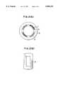
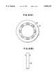
- FIGS. 6(A) and 6(B)are a cross sectional view and a side elevation view showing Ioffe bars another type for use in accordance with the present invention.
- the apparatuscomprises a reaction vacuum chamber 1 defining a resonating space therein, a loading chamber 8 connected with the vacuum chamber 1, a substrate holder 3 capable of carrying a substrate 2 to be treated, helmholts coils 5 around the reaction chamber 1, an auxiliary electro-magneto 6 located inside of the helmholtz coils around the reaction chamber, a mocrowave generator 4 connected to the reaction chamber 1 through a waveguide 7, an evacuating system 9, and gas feeding systems 10 and 11.
- the holder 3is made of a highly thermal conductive material, such as alminium nitride, which less disturb the microwave transmission from a microwave introduction window 12.
- FIG. 4is a graphical diagram showing the surfaces on which the magnetic field is constant when the auxiliary magnet is not used.
- a substrate 1is mounted on the holder 3 and disposed at an appropriate position in the reaction chamber 1 where the microwave and the magnetic field sutisfy the ECR contition.
- the substrate 1is heated to 500° C. and hydrogen gas is leaked into the chamber 1 at 10 SCCM through the gas feeding system 11.
- the introduced hydrogen gasis energized into a plasma gas by virtue of a 2.45 microwave emitted from the generator 4 and a magnetic field induced by both the helmholtz coils 5 and the auxiliary magnet 6.
- the strength of the portion of the magnetic field that is induced by the coils 5is about 2K Gauss at the resonating space (a partion of the reaction chamber).
- the pressure in the resonating spaceis maintained at 0.1 Pascal.
- the surface of the substrateis cleaned by virtue of the plasma.
- a halo patternwas observed at a relative low temperature together with a spot pattern which is peculier to amorphous structures. Such an image indicates the presence of i-carbon.
- the halo patterngradually distincted as the substrate temperature was elevated.
- the substrate temperaturewas elevated higher than 650° C.
- the deposited filmbecame composed mainly of diamond.
- the diamond filmwas confirmed by obtaining its Raman spectrum. The spectrum includes a moderate peak near 1500 cm -1 and a sharp peak near 1333 cm -1 .
- the above processcan be applied to a method of depositing polycrystalline silicon carbide films by making use of silicon carbide gaseous compounds as the reactive gas, to a method of depositing alminium nitride films by making use of a reactive gas consisting of an aluminium compound gas and ammonia, and a method of depositing films having a high melting point, e.g. films made of tungsten, titanium and molybdenum or their silicon compounds.
- the present inventioncan be applied for the deposition of BN, CN, TiN and BP.
- FIG. 5a schematic veiw showing another type of plasma processing apparatus.
- This apparatusis largely same as the above explained apparatus besides the relationship between the the helmholtz coils 5 and the connection position of the waveguide 7 to the reacion chamber 1.
- a microwaveis mixed with a reactive gas only in the left side of the center surface C between the helmholtz coils 5, so that the reactive gas is subjected to the magnetic field that is monotonically decreases toward the left in the resonating space.
- the magnetic fieldfunctions to drift the plamsa gas to the substrate 2 and prevent the gas from producing deposition on the right side wall.
- the present inventionshould be limited only by the appended claims and should not be limited by the particualr examles. What follow are some examples of modifications and variation according to the invention.
- the exciting plasma gasBy adding oxygen, water or the like to the reactive gas, the crystallinity of the deposited film can be enhanced.
- the exciting plasma gasBy irradiating the exciting plasma gas with ultraviolet rays between the resonating space and the substrate to be coated, the exciting plasma gas can hold its energy even substantially distant from the resonating space. For instance, a diamond or i-carbon film can be deposited on a large area.
- a DC bias voltageto the exciting plasma, a larger amount plasma reaches the substrate enabling a high deposition speed.
- the present inventionis effective when used for plasma etching, particularly by making use of ECR.
- the etchant gasis confined by virtue of the magnetic field in the same way as explained above.
Landscapes
- Chemical & Material Sciences (AREA)
- Engineering & Computer Science (AREA)
- Physics & Mathematics (AREA)
- Plasma & Fusion (AREA)
- Analytical Chemistry (AREA)
- Chemical Kinetics & Catalysis (AREA)
- General Chemical & Material Sciences (AREA)
- Materials Engineering (AREA)
- Mechanical Engineering (AREA)
- Metallurgy (AREA)
- Organic Chemistry (AREA)
- Chemical Vapour Deposition (AREA)
- ing And Chemical Polishing (AREA)
- Drying Of Semiconductors (AREA)
Abstract
Description
This is a Divisional application of Ser. No. 08/158,370, filed Nov. 29, 1993, U.S. Pat. No. 5,685,913; which itself is a continuation of Ser. No. 07/770,433, filed Sep. 26, 1991, now abandoned; which is a division of 07/461,938, filed Jan. 8, 1990, now abandoned; which is a division of Ser. No. 07/186,219, filed Apr. 26, 1988 (now U.S. Pat. No. 4,926,791).
This invention relates to a plasma processing apparatus and method.
There have been known the ECR CVD for depositing thin films on a substrate. In this deposition method, a substrate may be placed in a vacuum chamber apart from the resonating space and a thin film such as an amorphous film is formed on the substrate by virtue of a divergent magnetic field induced in the vacuum chamber.
The ECR CVD can be performed in combination with other known deposition methods such as heated filament CVD, chemical transportation method, plasma CVD making use of a high frequency power at 13.56 MHz, microwave-assisted CVD. In accordance with this method, a reactive gas is confined and excited by supplying a microwave under a magnetic field in accordance with the electron cycrotron resonance. The excited reactive gas is drifted to a substrate which is located at a position remote from the resonating space. At the remote position, the excited gas is deposited on the substrate or attacks to the substrate to effected anisotropic etching. The pressure in the chamber during process has been maintained at a relatively low pressure, e.g. of the order of 10-4 Torr. Because of this, it is very difficult to form a highly crystallized film such as a diamond film and to choose the process condition with a broad flexibility.
It is therefore an object of the invention to provide a plasma processing apparatus and method in which a highly energized plasma gas is confined about the center position at which a substrate to be processed is disposed.
It is therefore an object of the invention to provide a plasma processing apparatus and method in which highly crystallized films can be deposited under flexible condition.
According to one aspect of the invention, an auxiliary magnet is provided in addition to a main magnet which produces a magnetic field parallel with the microwave propagating direction allowing the plasma gas to resonating with the microwave. The auxiliary magnet is located along the wall of the reaction chamber for the purpose of enhancing the strength of magnetic field at the periphery of the reaction chamber. Since charged particles are subjected to a drifting force proportional to the minus of the gradient of the absolute strength of the magnetic field, plasma gas is confined in the center by virtue of the additional magnetic field induced by the auxiliary magnet.
The resonance taking place in the reaction chamber includes the electron cycrotron resonance, the whistler mode resonace, or other type resonance which is caused by supplying a microwave under a magnetic field such as the mixed cyclotron resonance. By virtue of such a resonance, a highly energized plasma gas having its high density is obtained. In case of carbon deposition, a highly energized plasma produces a large amount of excited carbon atoms and the high reproducibility is achieved.
In accordance with the most broad concept, it is noted that the present invention is also effective in case of thermal CVD, photo-assisted CVD or so forth in which no magnetic field is utilized. The reactive gas is confined in the vicinity where deposition is desired in the other deposition systems.
FIG. 1 is a schematic diagram showing a plasma processing apparatus for in accordance with the present invention.
FIGS. 2(A) and 2(B) are a cross sectional view and a side elevation view showing Ioffe bars for use in accordance with the present invention.
FIG. 3 is a graphical diagram showing the strength of magnetic field in a reaction chamber in accordance with the present invention.
FIG. 4 is a graphical diagram showing the strength of magnetic field induced only by helmholtz coils in a reaction chamber.
FIG. 5 is a schematic diagram showing another plasma processing apparatus for in accordance with the present invention.
FIGS. 6(A) and 6(B) are a cross sectional view and a side elevation view showing Ioffe bars another type for use in accordance with the present invention.
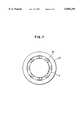
FIG. 7 is a cross sectional view Ioffe bars a further type for use in accordance with the present invention.
Referring to FIG. 1, a microwave assisted plasma-CVD apparatus in accordance with the present invention is illustrated. In the figure, the apparatus comprises areaction vacuum chamber 1 defining a resonating space therein, aloading chamber 8 connected with thevacuum chamber 1, a substrate holder 3 capable of carrying asubstrate 2 to be treated,helmholts coils 5 around thereaction chamber 1, an auxiliary electro-magneto 6 located inside of the helmholtz coils around the reaction chamber, amocrowave generator 4 connected to thereaction chamber 1 through awaveguide 7, an evacuatingsystem 9, andgas feeding systems 10 and 11. The holder 3 is made of a highly thermal conductive material, such as alminium nitride, which less disturb the microwave transmission from a microwave introduction window 12.
Theauxiliary magnet 6 consists of two electro-magnetos providing Ioffe bars which extend in the direction of the microwave propagation (FIGS. 2(A) and 2(B)). In FIG. 2(A), the end marks of arrow denote the current passing direction of each bar. The object of the provision of the Ioffe bars is to strengthen the strength of magnetic field near the cylindrical wall of thereaction chamber 1. FIG. 3 is a graphical diagram showing the surfaces on each of which the strength of the magnetic field is constant. The abscissa is the distance (r) from the axis of the cylindrical reaction chamber and the ordinate is the axial distance from the center plane of thehelmholtz coils 5. The figure given to each surface denotes the strength (Gauss) of the magnetic field on that surface. As shown in the diagram, the strength of the magnetic field takes a larger value at a nearer position to the cylindrical wall, so that the drifted force excerted on the plasma is alwalys centrifugal. The magnetic field is weakest on the axis of the cylindrical reaction chamber. FIG. 4 is a graphical diagram showing the surfaces on which the magnetic field is constant when the auxiliary magnet is not used.
Next, the deposition process with this apparatus will be described. Asubstrate 1 is mounted on the holder 3 and disposed at an appropriate position in thereaction chamber 1 where the microwave and the magnetic field sutisfy the ECR contition. After evacuating thereaction chamber 1, thesubstrate 1 is heated to 500° C. and hydrogen gas is leaked into thechamber 1 at 10 SCCM through the gas feeding system 11. The introduced hydrogen gas is energized into a plasma gas by virtue of a 2.45 microwave emitted from thegenerator 4 and a magnetic field induced by both thehelmholtz coils 5 and theauxiliary magnet 6. The strength of the portion of the magnetic field that is induced by thecoils 5 is about 2K Gauss at the resonating space (a partion of the reaction chamber). The pressure in the resonating space is maintained at 0.1 Pascal. The surface of the substrate is cleaned by virtue of the plasma.
Then, the introduction of hydrogen is halted and a carbon compound gas such as C2 H2 or CH4 is introduced into thereaction chamber 1 and excited in the same way as hydrogen as explained above. By this process, a diamond or i-carbon film is deposited on the substrate which has been heated to about 500° C. According to experimental, diamond films were deposited particularly when the substrate temperatures were not higher than 650° C.
In accordance with the electron beam detraction analysis, a halo pattern was observed at a relative low temperature together with a spot pattern which is peculier to amorphous structures. Such an image indicates the presence of i-carbon. The halo pattern gradually distincted as the substrate temperature was elevated. When the substrate temperature was elevated higher than 650° C., the deposited film became composed mainly of diamond. The diamond film was confirmed by obtaining its Raman spectrum. The spectrum includes a moderate peak near 1500 cm-1 and a sharp peak near 1333 cm-1.
For reference, the same process was repeated without inducing a magnetic field in the reaction chamber. The film thus deposited was made of graphite. Even with the presence of magnetic field, no i-carbon film could not be deposited on a substrate at a temperature lower than 150° C.
The above process can be applied to a method of depositing polycrystalline silicon carbide films by making use of silicon carbide gaseous compounds as the reactive gas, to a method of depositing alminium nitride films by making use of a reactive gas consisting of an aluminium compound gas and ammonia, and a method of depositing films having a high melting point, e.g. films made of tungsten, titanium and molybdenum or their silicon compounds. In the same way, the present invention can be applied for the deposition of BN, CN, TiN and BP.
FIG. 5 a schematic veiw showing another type of plasma processing apparatus. This apparatus is largely same as the above explained apparatus besides the relationship between the the helmholtz coils 5 and the connection position of thewaveguide 7 to thereacion chamber 1. In the arrangement, it is very important that a microwave is mixed with a reactive gas only in the left side of the center surface C between the helmholtz coils 5, so that the reactive gas is subjected to the magnetic field that is monotonically decreases toward the left in the resonating space. The magnetic field functions to drift the plamsa gas to thesubstrate 2 and prevent the gas from producing deposition on the right side wall.
The Ioffe magnet may be another type magnet. FIGS. 6(A) and 6(B) are drafted in correspondence with FIGS. 2(A) and 2(B) to show another type of Ioffe magnet sutable for use in accordance with the invention. As shown in the figure, a plurality of rod-shaped permanent magnets are arranged immediately inside of the helmholtz coils 5 with their magnetic moments directed to the circumferential direction as indicated by arrows. The magnetic moments can be arraged in the axial direction as shown in FIG. 7.
While a description has been made for several embodiments, the present invention should be limited only by the appended claims and should not be limited by the particualr examles. What follow are some examples of modifications and variation according to the invention. By adding oxygen, water or the like to the reactive gas, the crystallinity of the deposited film can be enhanced. By irradiating the exciting plasma gas with ultraviolet rays between the resonating space and the substrate to be coated, the exciting plasma gas can hold its energy even substantially distant from the resonating space. For instance, a diamond or i-carbon film can be deposited on a large area. Also, by applying a DC bias voltage to the exciting plasma, a larger amount plasma reaches the substrate enabling a high deposition speed. Also, as easily understood by those skilled in the art, the present invention is effective when used for plasma etching, particularly by making use of ECR. The etchant gas is confined by virtue of the magnetic field in the same way as explained above.
Claims (19)
1. A microwave plasma etching method comprising the steps of:
preparing a vacuum chamber having a central axis;
preparing at least a magnetic circuit provided around the periphery of said chamber;
preparing an even-number plurality of auxiliary magnets numbering at least two and provided around the periphery of said chamber and on the inner side of said magnetic circuit; and
preparing a microwave introducing means provided along the central axis of said chamber,
wherein the chamber is provided with a plasma-forming gas introducing port,
wherein the chamber has associated therewith a substrate to be etched,
wherein said auxiliary magnets are arranged symmetrically with respect to the central axis of said chamber in such a way that the magnetic poles of every auxiliary magnet are respectively reversed in polarity relative to the adjoining magnetic poles of an auxiliary magnet adjacent thereto,
wherein an electron cyclotron resonance phenomenon induced by an electric field formed by microwaves introduced into said chamber through said microwave introducing means and a magnetic field formed by means of said magnetic circuit and said auxiliary magnets is utilized to turn a plasma-forming gas introduced into said chamber into a plasma to thus etch the substrate, and
wherein said substrate is located at substantially an ECR point in the chamber where said electron cyclotron resonance occurs.
2. A method according to claim 1 wherein said auxiliary magnets are each constituted of a permanent magnet.
3. A plasma etching method comprising the steps of:
preparing a vacuum chamber having a central axis;
introducing a process gas into said vacuum chamber;
introducing a microwave into said vacuum chamber in a direction parallel to said central axis thereof;
preparing a substrate holder for holding a substrate in said vacuum chamber;
establishing a first magnetic field in said vacuum chamber in order to excite said gas into a plasma by an interaction between said first magnetic field and said microwave where said substrate is located substantially at an electron cyclotron resonance point in said vacuum chamber where said microwave and first magnetic field satisfy the condition for electron cyclotron resonance; and
establishing a second magnetic field in said vacuum chamber, said second magnetic field being such that said plasma is forced to move away from inner walls of said vacuum chamber by said second magnetic field.
4. A method according to claim 3 wherein said first magnetic field is substantially in parallel with the central axis of said vacuum chamber.
5. A method according to claim 4 wherein said second magnetic field is substantially perpendicular to the central axis of said vacuum chamber.
6. A method according to claim 3 further comprising the step of deposition of etching processes.
7. A plasma etching method comprising the steps of:
preparing at least a magnetic circuit provided around the periphery of a chamber;
preparing an even-numbered plurality of auxiliary magnets numbering at least two and provided around the periphery of said chamber and on the inner side of said magnetic circuit; and
preparing a microwave introducing means provided along the central axis of said chamber;
wherein the chamber has associated therewith a substrate to be etched,
wherein said auxiliary magnets are arranged symmetrically with respect to the central axis of said chamber in such a way that the magnetic poles of every auxiliary magnet are respectively reversed in polarity relative to adjoining magnetic poles of an auxiliary magnet adjacent thereto,
wherein an electron cyclotron resonance phenomenon induced by an electric field formed by microwaves introduced into said chamber through said microwave introducing means and a magnetic field formed by means of said magnetic circuit and said auxiliary magnets is utilized to turn a plasma-forming gas introduced into said chamber into a plasma to thus etch the substrate.
8. A method according to claim 7 wherein said auxiliary magnets are each constituted of a permanent magnet.
9. A plasma etching method comprising the steps of:
preparing a vacuum chamber having a central axis;
introducing a process gas into said vacuum chamber;
introducing a microwave into said vacuum chamber in a direction parallel to said central axis thereof;
preparing a substrate holder for holding a substrate in said vacuum chamber;
establishing a first magnetic field in said vacuum chamber in order to excite said gas into a plasma by an interaction between said first magnetic field and said microwave; and
establishing a second magnetic field in said field in said vacuum chamber, said second magnetic field is such that said plasma is forced to move away from inner walls of said vacuum chamber by said second magnetic field.
10. A method according to claim 9 wherein said first magnetic field is subtantially in parallel with the central axis of said vacuum chamber.
11. A method according to claim 9 wherein said second magnetic field is substantially perpendicular to the central axis of said vacuum chamber.
12. A plasma processing method comprising the steps of:
preparing a vacuum chamber having a central axis;
preparing a substrate holder for supporting a substrate in said vacuum chamber;
introducing a process gas into said vacuum chamber;
introducing a microwave into said vacuum chamber in a direction parallel to said central axis;
inducing a first magnetic field in said vacuum chamber in order to excite said process gas into a plasma by an interaction between said first magnetic field and said microwave;
preparing a vacuum pump for evacuating said vacuum chamber; and
establishing a second magnetic field in said vacuum chamber, said second magnetic field is such that said plasma is forced to move away from inner walls of said vacuum chamber by said second magnetic field.
13. A method according to claim 12 wherein said second magnetic field is established by Ioffe bars.
14. A method according to claim 13 wherein said Ioffe bars comprise a plurality of coils arranged around said vacuum chamber.
15. A method according to claim 13 wherein said Ioffe bars are a plurality of permanent magnet rods, each having its magnetic moment along the circumferential direction of said Helmholtz coils.
16. A method according to claim 15 wherein senses of the magnetic moments of the Ioffe bars are alternating.
17. A plasma processing method comprising the steps of:
preparing a vacuum chamber having inner walls and a central axis;
preparing a substrate holder for supporting a substrate in said vacuum chamber;
introducing a reactive gas into said vacuum chamber in a direction parallel to said central axis thereof;
forming a first magnetic field in said vacuum chamber in order to form a plasma of said reactive gas by an interaction with said microwaves where said substrate is located substantially at an electron cyclotron resonance point in said vacuum chamber where said microwaves and said first magnetic field satisfy the condition for electron cyclotron resonance; and
forming a second magnetic field in said vacuum chamber in order to force away said plasma from the inner walls of said vacuum chamber.
18. A method according to claim 17 further comprising the step of plasma etching on said substrate.
19. A method according to claim 18 wherein said etching is an anisotropic etching.
Priority Applications (5)
| Application Number | Priority Date | Filing Date | Title |
|---|---|---|---|
| US08/892,267US5858259A (en) | 1987-04-27 | 1997-07-14 | Plasma processing apparatus and method |
| US09/196,744US6217661B1 (en) | 1987-04-27 | 1998-11-20 | Plasma processing apparatus and method |
| US09/196,141US6423383B1 (en) | 1987-04-27 | 1998-11-20 | Plasma processing apparatus and method |
| US10/189,422US6838126B2 (en) | 1987-04-27 | 2002-07-08 | Method for forming I-carbon film |
| US11/022,812US20050106331A1 (en) | 1987-04-27 | 2004-12-28 | Plasma processing apparatus and method |
Applications Claiming Priority (9)
| Application Number | Priority Date | Filing Date | Title |
|---|---|---|---|
| JP62-104025 | 1987-04-27 | ||
| JP62-104024 | 1987-04-27 | ||
| JP10402587 | 1987-04-27 | ||
| JP10402487 | 1987-04-27 | ||
| US07/186,219US4926791A (en) | 1987-04-27 | 1988-04-26 | Microwave plasma apparatus employing helmholtz coils and ioffe bars |
| US46193890A | 1990-01-08 | 1990-01-08 | |
| US77043391A | 1991-09-26 | 1991-09-26 | |
| US08/158,370US5685913A (en) | 1987-04-27 | 1993-11-29 | Plasma processing apparatus and method |
| US08/892,267US5858259A (en) | 1987-04-27 | 1997-07-14 | Plasma processing apparatus and method |
Related Parent Applications (1)
| Application Number | Title | Priority Date | Filing Date |
|---|---|---|---|
| US08/158,370DivisionUS5685913A (en) | 1987-04-27 | 1993-11-29 | Plasma processing apparatus and method |
Related Child Applications (2)
| Application Number | Title | Priority Date | Filing Date |
|---|---|---|---|
| US09/196,744DivisionUS6217661B1 (en) | 1987-04-27 | 1998-11-20 | Plasma processing apparatus and method |
| US09/196,141DivisionUS6423383B1 (en) | 1987-04-27 | 1998-11-20 | Plasma processing apparatus and method |
Publications (1)
| Publication Number | Publication Date |
|---|---|
| US5858259Atrue US5858259A (en) | 1999-01-12 |
Family
ID=26444581
Family Applications (7)
| Application Number | Title | Priority Date | Filing Date |
|---|---|---|---|
| US07/186,219Expired - LifetimeUS4926791A (en) | 1987-04-27 | 1988-04-26 | Microwave plasma apparatus employing helmholtz coils and ioffe bars |
| US08/158,370Expired - Fee RelatedUS5685913A (en) | 1987-04-27 | 1993-11-29 | Plasma processing apparatus and method |
| US08/892,267Expired - Fee RelatedUS5858259A (en) | 1987-04-27 | 1997-07-14 | Plasma processing apparatus and method |
| US09/196,141Expired - Fee RelatedUS6423383B1 (en) | 1987-04-27 | 1998-11-20 | Plasma processing apparatus and method |
| US09/196,744Expired - Fee RelatedUS6217661B1 (en) | 1987-04-27 | 1998-11-20 | Plasma processing apparatus and method |
| US10/189,422Expired - Fee RelatedUS6838126B2 (en) | 1987-04-27 | 2002-07-08 | Method for forming I-carbon film |
| US11/022,812AbandonedUS20050106331A1 (en) | 1987-04-27 | 2004-12-28 | Plasma processing apparatus and method |
Family Applications Before (2)
| Application Number | Title | Priority Date | Filing Date |
|---|---|---|---|
| US07/186,219Expired - LifetimeUS4926791A (en) | 1987-04-27 | 1988-04-26 | Microwave plasma apparatus employing helmholtz coils and ioffe bars |
| US08/158,370Expired - Fee RelatedUS5685913A (en) | 1987-04-27 | 1993-11-29 | Plasma processing apparatus and method |
Family Applications After (4)
| Application Number | Title | Priority Date | Filing Date |
|---|---|---|---|
| US09/196,141Expired - Fee RelatedUS6423383B1 (en) | 1987-04-27 | 1998-11-20 | Plasma processing apparatus and method |
| US09/196,744Expired - Fee RelatedUS6217661B1 (en) | 1987-04-27 | 1998-11-20 | Plasma processing apparatus and method |
| US10/189,422Expired - Fee RelatedUS6838126B2 (en) | 1987-04-27 | 2002-07-08 | Method for forming I-carbon film |
| US11/022,812AbandonedUS20050106331A1 (en) | 1987-04-27 | 2004-12-28 | Plasma processing apparatus and method |
Country Status (2)
| Country | Link |
|---|---|
| US (7) | US4926791A (en) |
| JP (1) | JPH0672306B2 (en) |
Cited By (6)
| Publication number | Priority date | Publication date | Assignee | Title |
|---|---|---|---|---|
| US6022460A (en)* | 1999-01-18 | 2000-02-08 | Inha University Foundation | Enhanced inductively coupled plasma reactor |
| US6390019B1 (en)* | 1998-06-11 | 2002-05-21 | Applied Materials, Inc. | Chamber having improved process monitoring window |
| US20030021910A1 (en)* | 1987-04-27 | 2003-01-30 | Semiconductor Energy Laboratory Co., Ltd. | Plasma processing apparatus and method |
| US6673199B1 (en) | 2001-03-07 | 2004-01-06 | Applied Materials, Inc. | Shaping a plasma with a magnetic field to control etch rate uniformity |
| US20080272089A1 (en)* | 1997-10-06 | 2008-11-06 | Applied Materials, Inc. | Monitoring etching of a substrate in an etch chamber |
| US20100257037A1 (en)* | 2001-12-14 | 2010-10-07 | Matz William R | Method and system for targeted incentives |
Families Citing this family (47)
| Publication number | Priority date | Publication date | Assignee | Title |
|---|---|---|---|---|
| US5203959A (en)* | 1987-04-27 | 1993-04-20 | Semiconductor Energy Laboratory Co., Ltd. | Microwave plasma etching and deposition method employing first and second magnetic fields |
| KR920002864B1 (en)* | 1987-07-20 | 1992-04-06 | 가부시기가이샤 히다찌세이사꾸쇼 | Apparatus for treating matrial by using plasma |
| JPH0668152B2 (en)* | 1988-01-27 | 1994-08-31 | 株式会社半導体エネルギー研究所 | Thin film forming equipment |
| EP0402867B1 (en)* | 1989-06-15 | 1995-03-01 | Sel Semiconductor Energy Laboratory Co., Ltd. | Apparatus for microwave processing in a magnetic field |
| JP2711580B2 (en)* | 1990-01-12 | 1998-02-10 | アルプス電気株式会社 | Molding mold manufacturing method |
| JPH0821578B2 (en)* | 1990-03-12 | 1996-03-04 | ▲あきら▼ 太田 | Microwave plasma generator |
| US5071670A (en)* | 1990-06-11 | 1991-12-10 | Kelly Michael A | Method for chemical vapor deposition under a single reactor vessel divided into separate reaction chambers each with its own depositing and exhausting means |
| JPH04129133A (en)* | 1990-09-20 | 1992-04-30 | Hitachi Ltd | Ion source and plasma device |
| DE4235199C1 (en) | 1992-10-19 | 1993-04-22 | Fraunhofer-Gesellschaft Zur Foerderung Der Angewandten Forschung Ev, 8000 Muenchen, De | |
| FI110014B (en)* | 1996-10-23 | 2002-11-15 | Metso Paper Inc | Method for sliding the roller sheath of a preformed roller of a paper machine or its equivalent and a sliding roller |
| US6163055A (en)* | 1997-03-24 | 2000-12-19 | Semiconductor Energy Laboratory Co., Ltd | Semiconductor device and manufacturing method thereof |
| US6927826B2 (en)* | 1997-03-26 | 2005-08-09 | Semiconductor Energy Labaratory Co., Ltd. | Display device |
| JPH11193468A (en)* | 1997-12-30 | 1999-07-21 | Shimadzu Corp | Thin film forming equipment |
| US6313587B1 (en) | 1998-01-13 | 2001-11-06 | Fusion Lighting, Inc. | High frequency inductive lamp and power oscillator |
| US6137237A (en) | 1998-01-13 | 2000-10-24 | Fusion Lighting, Inc. | High frequency inductive lamp and power oscillator |
| JP3189780B2 (en)* | 1998-03-24 | 2001-07-16 | 日本電気株式会社 | Apparatus and method for manufacturing semiconductor device |
| JPH11307782A (en) | 1998-04-24 | 1999-11-05 | Semiconductor Energy Lab Co Ltd | Semiconductor device and manufacturing method thereof |
| US6475836B1 (en) | 1999-03-29 | 2002-11-05 | Semiconductor Energy Laboratory Co., Ltd. | Semiconductor device and manufacturing method thereof |
| FR2795906B1 (en)* | 1999-07-01 | 2001-08-17 | Commissariat Energie Atomique | PROCESS AND DEVICE FOR PLASMA DEPOSIT AT THE ELECTRONIC CYCLOTRON RESONANCE OF LAYERS OF CARBON NONOFIBRES TISSUES AND LAYERS OF TISSUES THUS OBTAINED |
| DE10018143C5 (en)* | 2000-04-12 | 2012-09-06 | Oerlikon Trading Ag, Trübbach | DLC layer system and method and apparatus for producing such a layer system |
| DE10026540A1 (en)* | 2000-05-27 | 2001-11-29 | Gfe Met & Mat Gmbh | Object, especially implant |
| JP4008728B2 (en)* | 2002-03-20 | 2007-11-14 | 株式会社 液晶先端技術開発センター | Plasma processing equipment |
| US20080096800A1 (en)* | 2004-03-12 | 2008-04-24 | Biodel, Inc. | Rapid mucosal gel or film insulin compositions |
| EP2251454B1 (en) | 2009-05-13 | 2014-07-23 | SiO2 Medical Products, Inc. | Vessel coating and inspection |
| WO2013170052A1 (en) | 2012-05-09 | 2013-11-14 | Sio2 Medical Products, Inc. | Saccharide protective coating for pharmaceutical package |
| US9458536B2 (en) | 2009-07-02 | 2016-10-04 | Sio2 Medical Products, Inc. | PECVD coating methods for capped syringes, cartridges and other articles |
| US8301408B2 (en)* | 2010-03-09 | 2012-10-30 | Invensys Systems, Inc. | Temperature prediction transmitter |
| US11624115B2 (en) | 2010-05-12 | 2023-04-11 | Sio2 Medical Products, Inc. | Syringe with PECVD lubrication |
| US9878101B2 (en) | 2010-11-12 | 2018-01-30 | Sio2 Medical Products, Inc. | Cyclic olefin polymer vessels and vessel coating methods |
| US9272095B2 (en) | 2011-04-01 | 2016-03-01 | Sio2 Medical Products, Inc. | Vessels, contact surfaces, and coating and inspection apparatus and methods |
| US11116695B2 (en) | 2011-11-11 | 2021-09-14 | Sio2 Medical Products, Inc. | Blood sample collection tube |
| CA2855353C (en) | 2011-11-11 | 2021-01-19 | Sio2 Medical Products, Inc. | Passivation, ph protective or lubricity coating for pharmaceutical package, coating process and apparatus |
| JP5836144B2 (en)* | 2012-01-31 | 2015-12-24 | 東京エレクトロン株式会社 | Microwave radiation mechanism and surface wave plasma processing equipment |
| US20150297800A1 (en) | 2012-07-03 | 2015-10-22 | Sio2 Medical Products, Inc. | SiOx BARRIER FOR PHARMACEUTICAL PACKAGE AND COATING PROCESS |
| US9664626B2 (en) | 2012-11-01 | 2017-05-30 | Sio2 Medical Products, Inc. | Coating inspection method |
| US9903782B2 (en) | 2012-11-16 | 2018-02-27 | Sio2 Medical Products, Inc. | Method and apparatus for detecting rapid barrier coating integrity characteristics |
| US9764093B2 (en) | 2012-11-30 | 2017-09-19 | Sio2 Medical Products, Inc. | Controlling the uniformity of PECVD deposition |
| AU2013352436B2 (en) | 2012-11-30 | 2018-10-25 | Sio2 Medical Products, Inc. | Controlling the uniformity of PECVD deposition on medical syringes, cartridges, and the like |
| US20160015898A1 (en) | 2013-03-01 | 2016-01-21 | Sio2 Medical Products, Inc. | Plasma or cvd pre-treatment for lubricated pharmaceutical package, coating process and apparatus |
| US9937099B2 (en) | 2013-03-11 | 2018-04-10 | Sio2 Medical Products, Inc. | Trilayer coated pharmaceutical packaging with low oxygen transmission rate |
| JP6453841B2 (en) | 2013-03-11 | 2019-01-16 | エスアイオーツー・メディカル・プロダクツ・インコーポレイテッド | Coated packaging |
| US20160017490A1 (en) | 2013-03-15 | 2016-01-21 | Sio2 Medical Products, Inc. | Coating method |
| US9435031B2 (en) | 2014-01-07 | 2016-09-06 | International Business Machines Corporation | Microwave plasma and ultraviolet assisted deposition apparatus and method for material deposition using the same |
| EP3122917B1 (en) | 2014-03-28 | 2020-05-06 | SiO2 Medical Products, Inc. | Antistatic coatings for plastic vessels |
| US10151025B2 (en)* | 2014-07-31 | 2018-12-11 | Seagate Technology Llc | Helmholtz coil assisted PECVD carbon source |
| KR102786617B1 (en) | 2015-08-18 | 2025-03-26 | 에스아이오2 메디컬 프로덕츠, 엘엘씨 | Packaging containers for pharmaceuticals and other products with low oxygen permeability |
| JP2023515564A (en)* | 2020-02-24 | 2023-04-13 | エム・セブン・ディー コーポレーション | Plasma shaping for diamond growth |
Citations (25)
| Publication number | Priority date | Publication date | Assignee | Title |
|---|---|---|---|---|
| US4125431A (en)* | 1977-06-16 | 1978-11-14 | The United States Of America As Represented By The United States Department Of Energy | Tandem mirror plasma confinement apparatus |
| US4354999A (en)* | 1976-12-20 | 1982-10-19 | Priest Robert V | Plasma confinement |
| US4430138A (en)* | 1979-04-06 | 1984-02-07 | Hitachi, Ltd. | Microwave plasma etching apparatus having fan-shaped discharge |
| US4434188A (en)* | 1981-12-17 | 1984-02-28 | National Institute For Researches In Inorganic Materials | Method for synthesizing diamond |
| JPS59136130A (en)* | 1983-01-24 | 1984-08-04 | Hitachi Ltd | Device for forming plasma film by microwave |
| JPS60115235A (en)* | 1983-11-26 | 1985-06-21 | Nippon Telegr & Teleph Corp <Ntt> | Formimg method of insulation film on compound semiconductor substrate |
| US4559100A (en)* | 1983-12-23 | 1985-12-17 | Hitachi, Ltd. | Microwave plasma etching apparatus |
| JPS6147628A (en)* | 1984-08-13 | 1986-03-08 | Nippon Telegr & Teleph Corp <Ntt> | Formation of semiconductor thin film and apparatus therefor |
| US4609428A (en)* | 1984-07-23 | 1986-09-02 | Fujitsu Limited | Method and apparatus for microwave plasma anisotropic dry etching |
| JPS61213377A (en)* | 1985-03-18 | 1986-09-22 | Hitachi Ltd | Method and apparatus for plasma deposition |
| JPS61267324A (en)* | 1985-05-21 | 1986-11-26 | Fuji Electric Co Ltd | Dry thin film processing equipment |
| JPS627859A (en)* | 1985-07-05 | 1987-01-14 | Hitachi Ltd | Formation of amorphous silicon film |
| EP0209109A2 (en)* | 1985-07-15 | 1987-01-21 | Hitachi, Ltd. | Method of and apparatus for forming film by utilizing low-temperature plasma |
| EP0209469A1 (en)* | 1985-06-07 | 1987-01-21 | ETAT FRANCAIS représenté par le Ministre des PTT (Centre National d'Etudes des Télécommunications) | Method and apparatus for microwave excitation of a plasma at the electron cyclotron resonance |
| JPS6230891A (en)* | 1985-08-02 | 1987-02-09 | Hitachi Ltd | Dry etching method |
| JPS62115821A (en)* | 1985-11-15 | 1987-05-27 | Hitachi Ltd | Low temperature plasma processing device |
| US4727293A (en)* | 1984-08-16 | 1988-02-23 | Board Of Trustees Operating Michigan State University | Plasma generating apparatus using magnets and method |
| JPS6343324A (en)* | 1986-08-09 | 1988-02-24 | Anelva Corp | plasma shower device |
| JPS63103098A (en)* | 1986-10-20 | 1988-05-07 | Nippon Steel Corp | Surface treatment of amorphous alloy material |
| JPS63217620A (en)* | 1987-03-06 | 1988-09-09 | Hitachi Ltd | plasma processing equipment |
| US4778561A (en)* | 1987-10-30 | 1988-10-18 | Veeco Instruments, Inc. | Electron cyclotron resonance plasma source |
| US4926791A (en)* | 1987-04-27 | 1990-05-22 | Semiconductor Energy Laboratory Co., Ltd. | Microwave plasma apparatus employing helmholtz coils and ioffe bars |
| US4960073A (en)* | 1988-09-19 | 1990-10-02 | Anelva Corporation | Microwave plasma treatment apparatus |
| US4973883A (en)* | 1987-05-01 | 1990-11-27 | Semiconductor Energy Laborator Co., Ltd. | Plasma processing apparatus with a lisitano coil |
| US5039548A (en)* | 1988-01-27 | 1991-08-13 | Semiconductor Energy Laboratory Co., Ltd. | Plasma chemical vapor reaction method employing cyclotron resonance |
Family Cites Families (45)
| Publication number | Priority date | Publication date | Assignee | Title |
|---|---|---|---|---|
| DE1900116C3 (en) | 1969-01-02 | 1978-10-19 | Siemens Ag, 1000 Berlin Und 8000 Muenchen | Process for the production of high-purity monocrystalline layers consisting of silicon |
| US3911318A (en) | 1972-03-29 | 1975-10-07 | Fusion Systems Corp | Method and apparatus for generating electromagnetic radiation |
| US4047496A (en) | 1974-05-31 | 1977-09-13 | Applied Materials, Inc. | Epitaxial radiation heated reactor |
| GB2069008B (en)* | 1980-01-16 | 1984-09-12 | Secr Defence | Coating in a glow discharge |
| CA1159012A (en) | 1980-05-02 | 1983-12-20 | Seitaro Matsuo | Plasma deposition apparatus |
| JPS5740586A (en) | 1980-08-22 | 1982-03-06 | Toshiba Corp | Treatment of fluorescent substance and its device |
| JPS5779621A (en) | 1980-11-05 | 1982-05-18 | Mitsubishi Electric Corp | Plasma processing device |
| JPH0635323B2 (en) | 1982-06-25 | 1994-05-11 | 株式会社日立製作所 | Surface treatment method |
| EP0102489B1 (en) | 1982-07-31 | 1987-02-04 | BROWN, BOVERI & CIE Aktiengesellschaft | Multifilament superconductor and method of making the same |
| JPS5963732A (en) | 1982-10-04 | 1984-04-11 | Hitachi Ltd | Thin film forming equipment |
| US4513684A (en) | 1982-12-22 | 1985-04-30 | Energy Conversion Devices, Inc. | Upstream cathode assembly |
| JPS59159167A (en) | 1983-03-01 | 1984-09-08 | Zenko Hirose | Manufacture of amorphous silicon film |
| JPS59222922A (en) | 1983-06-01 | 1984-12-14 | Nippon Telegr & Teleph Corp <Ntt> | Vapor growth apparatus |
| JPS6037129A (en) | 1983-08-10 | 1985-02-26 | Hitachi Ltd | Equipment for manufacturing semiconductor |
| KR890004881B1 (en)* | 1983-10-19 | 1989-11-30 | 가부시기가이샤 히다찌세이사꾸쇼 | Plasma treatment method and apparatus |
| JPS60103098A (en) | 1983-11-04 | 1985-06-07 | Kyocera Corp | Manufacture of diamond film |
| JPS60170234A (en) | 1984-02-15 | 1985-09-03 | Semiconductor Energy Lab Co Ltd | Vapor-phase reaction apparatus and manufacture of vapor-phase reaction film |
| JPS60234403A (en) | 1984-05-04 | 1985-11-21 | Hitachi Ltd | electric car control device |
| DE3421739C2 (en)* | 1984-06-12 | 1987-01-02 | Battelle-Institut E.V., 6000 Frankfurt | Process for producing diamond-like carbon layers |
| JPS6113626A (en) | 1984-06-29 | 1986-01-21 | Hitachi Ltd | plasma processing equipment |
| JPS6123377A (en) | 1984-07-12 | 1986-01-31 | Nec Corp | Plane optical waveguide with output-stabilized laser |
| JPS6136200A (en) | 1984-07-25 | 1986-02-20 | Sumitomo Electric Ind Ltd | Method for vapor-phase synthesis of diamond |
| US4663183A (en)* | 1984-09-10 | 1987-05-05 | Energy Conversion Devices, Inc. | Glow discharge method of applying a carbon coating onto a substrate |
| JPH0715898B2 (en) | 1984-12-24 | 1995-02-22 | 株式会社日立製作所 | Microwave plasma processing equipment |
| JPS61158898A (en) | 1984-12-29 | 1986-07-18 | Kyocera Corp | Production of ornamental diamond |
| US4640224A (en) | 1985-08-05 | 1987-02-03 | Spectrum Cvd, Inc. | CVD heat source |
| JPS6265997A (en)* | 1985-09-18 | 1987-03-25 | Nippon Soken Inc | Method and apparatus for synthesizing diamond |
| JPH07100857B2 (en) | 1985-10-09 | 1995-11-01 | 株式会社日立製作所 | Carbon film forming method and apparatus |
| JPS6296397A (en) | 1985-10-22 | 1987-05-02 | Asahi Chem Ind Co Ltd | Diamond manufacturing method |
| JPS6380523A (en) | 1986-09-24 | 1988-04-11 | Matsushita Electric Ind Co Ltd | Microwave plasma processing equipment |
| JPS6383271A (en)* | 1986-09-25 | 1988-04-13 | Canon Inc | Production of diamond-like carbon film |
| JPS6385092A (en)* | 1986-09-26 | 1988-04-15 | Tdk Corp | Production of diamond film |
| US4776918A (en) | 1986-10-20 | 1988-10-11 | Hitachi, Ltd. | Plasma processing apparatus |
| US5266363A (en) | 1986-11-10 | 1993-11-30 | Semiconductor Energy Laboratory Co., Ltd. | Plasma processing method utilizing a microwave and a magnetic field at high pressure |
| US6677001B1 (en)* | 1986-11-10 | 2004-01-13 | Semiconductor Energy Laboratory Co., Ltd. | Microwave enhanced CVD method and apparatus |
| DE3853890T2 (en) | 1987-01-19 | 1995-10-19 | Hitachi Ltd | Device working with a plasma. |
| JPS63195266A (en) | 1987-02-10 | 1988-08-12 | Semiconductor Energy Lab Co Ltd | Timepiece coated with carbon film |
| KR900008505B1 (en)* | 1987-02-24 | 1990-11-24 | 세미콘덕터 에너지 라보라터리 캄파니 리미티드 | Microwave Enhanced CVD Method for Carbon Precipitation |
| JPS63225528A (en) | 1987-03-13 | 1988-09-20 | Toa Nenryo Kogyo Kk | Production of superconductive compound oxide |
| US5203959A (en)* | 1987-04-27 | 1993-04-20 | Semiconductor Energy Laboratory Co., Ltd. | Microwave plasma etching and deposition method employing first and second magnetic fields |
| JPH0791152B2 (en) | 1987-08-31 | 1995-10-04 | 松下電器産業株式会社 | Method for manufacturing superconductor thin film |
| KR910007384B1 (en) | 1987-09-16 | 1991-09-25 | 가부시끼가이샤 한도다이 에네르기 겐뀨쇼 | Formation of superconductor oxide film |
| JPH0817253B2 (en) | 1987-09-16 | 1996-02-21 | 株式会社半導体エネルギー研究所 | Method for forming oxide superconducting film |
| US5079031A (en)* | 1988-03-22 | 1992-01-07 | Semiconductor Energy Laboratory Co., Ltd. | Apparatus and method for forming thin films |
| JPH02141494A (en)* | 1988-07-30 | 1990-05-30 | Kobe Steel Ltd | Vapor phase synthetic device of diamond |
- 1988
- 1988-04-26JPJP63103093Apatent/JPH0672306B2/ennot_activeExpired - Lifetime
- 1988-04-26USUS07/186,219patent/US4926791A/ennot_activeExpired - Lifetime
- 1993
- 1993-11-29USUS08/158,370patent/US5685913A/ennot_activeExpired - Fee Related
- 1997
- 1997-07-14USUS08/892,267patent/US5858259A/ennot_activeExpired - Fee Related
- 1998
- 1998-11-20USUS09/196,141patent/US6423383B1/ennot_activeExpired - Fee Related
- 1998-11-20USUS09/196,744patent/US6217661B1/ennot_activeExpired - Fee Related
- 2002
- 2002-07-08USUS10/189,422patent/US6838126B2/ennot_activeExpired - Fee Related
- 2004
- 2004-12-28USUS11/022,812patent/US20050106331A1/ennot_activeAbandoned
Patent Citations (25)
| Publication number | Priority date | Publication date | Assignee | Title |
|---|---|---|---|---|
| US4354999A (en)* | 1976-12-20 | 1982-10-19 | Priest Robert V | Plasma confinement |
| US4125431A (en)* | 1977-06-16 | 1978-11-14 | The United States Of America As Represented By The United States Department Of Energy | Tandem mirror plasma confinement apparatus |
| US4430138A (en)* | 1979-04-06 | 1984-02-07 | Hitachi, Ltd. | Microwave plasma etching apparatus having fan-shaped discharge |
| US4434188A (en)* | 1981-12-17 | 1984-02-28 | National Institute For Researches In Inorganic Materials | Method for synthesizing diamond |
| JPS59136130A (en)* | 1983-01-24 | 1984-08-04 | Hitachi Ltd | Device for forming plasma film by microwave |
| JPS60115235A (en)* | 1983-11-26 | 1985-06-21 | Nippon Telegr & Teleph Corp <Ntt> | Formimg method of insulation film on compound semiconductor substrate |
| US4559100A (en)* | 1983-12-23 | 1985-12-17 | Hitachi, Ltd. | Microwave plasma etching apparatus |
| US4609428A (en)* | 1984-07-23 | 1986-09-02 | Fujitsu Limited | Method and apparatus for microwave plasma anisotropic dry etching |
| JPS6147628A (en)* | 1984-08-13 | 1986-03-08 | Nippon Telegr & Teleph Corp <Ntt> | Formation of semiconductor thin film and apparatus therefor |
| US4727293A (en)* | 1984-08-16 | 1988-02-23 | Board Of Trustees Operating Michigan State University | Plasma generating apparatus using magnets and method |
| JPS61213377A (en)* | 1985-03-18 | 1986-09-22 | Hitachi Ltd | Method and apparatus for plasma deposition |
| JPS61267324A (en)* | 1985-05-21 | 1986-11-26 | Fuji Electric Co Ltd | Dry thin film processing equipment |
| EP0209469A1 (en)* | 1985-06-07 | 1987-01-21 | ETAT FRANCAIS représenté par le Ministre des PTT (Centre National d'Etudes des Télécommunications) | Method and apparatus for microwave excitation of a plasma at the electron cyclotron resonance |
| JPS627859A (en)* | 1985-07-05 | 1987-01-14 | Hitachi Ltd | Formation of amorphous silicon film |
| EP0209109A2 (en)* | 1985-07-15 | 1987-01-21 | Hitachi, Ltd. | Method of and apparatus for forming film by utilizing low-temperature plasma |
| JPS6230891A (en)* | 1985-08-02 | 1987-02-09 | Hitachi Ltd | Dry etching method |
| JPS62115821A (en)* | 1985-11-15 | 1987-05-27 | Hitachi Ltd | Low temperature plasma processing device |
| JPS6343324A (en)* | 1986-08-09 | 1988-02-24 | Anelva Corp | plasma shower device |
| JPS63103098A (en)* | 1986-10-20 | 1988-05-07 | Nippon Steel Corp | Surface treatment of amorphous alloy material |
| JPS63217620A (en)* | 1987-03-06 | 1988-09-09 | Hitachi Ltd | plasma processing equipment |
| US4926791A (en)* | 1987-04-27 | 1990-05-22 | Semiconductor Energy Laboratory Co., Ltd. | Microwave plasma apparatus employing helmholtz coils and ioffe bars |
| US4973883A (en)* | 1987-05-01 | 1990-11-27 | Semiconductor Energy Laborator Co., Ltd. | Plasma processing apparatus with a lisitano coil |
| US4778561A (en)* | 1987-10-30 | 1988-10-18 | Veeco Instruments, Inc. | Electron cyclotron resonance plasma source |
| US5039548A (en)* | 1988-01-27 | 1991-08-13 | Semiconductor Energy Laboratory Co., Ltd. | Plasma chemical vapor reaction method employing cyclotron resonance |
| US4960073A (en)* | 1988-09-19 | 1990-10-02 | Anelva Corporation | Microwave plasma treatment apparatus |
Non-Patent Citations (9)
| Title |
|---|
| "An Optimum Condition of Multipole Field for an ECR-Type Ion Source", Jap. Journal of Appl. Phys., vol. 25, No. 9, Sep. 1986 by Ishii et al., pp. L712-L715. |
| "ECR Type Ion Source", Proc. 10th Symp. on ISIAT '86. (Tokyo, 1986), pp. 117-120 by M. Tamba, Y. Ishibe and Y. Sakamoto. |
| "Suppression of Noise in a Discharge Tube by a Minimum-B Type Magnet", Jap. Journal of Appl. Phys., vol. 27, No. 2, Feb. 1988, by Hiroshi Amemiya, pp. 297-301. |
| An Optimum Condition of Multipole Field for an ECR Type Ion Source , Jap. Journal of Appl. Phys., vol. 25, No. 9, Sep. 1986 by Ishii et al., pp. L712 L715.* |
| Bachmann et al., Emerging Technology of Diamond Thin Films (pp. 24,32) May 15, 1989 C&EN.* |
| ECR Type Ion Source , Proc. 10th Symp. on ISIAT 86. (Tokyo, 1986), pp. 117 120 by M. Tamba, Y. Ishibe and Y. Sakamoto.* |
| Suppression of Noise in a Discharge Tube by a Minimum B Type Magnet , Jap. Journal of Appl. Phys., vol. 27, No. 2, Feb. 1988, by Hiroshi Amemiya, pp. 297 301.* |
| Y. Arnal et al. "Plasma Etching in Magnetic Multipole Microwave Discharge" Appl. Phys. Lett 45(2) 15 Jul. 1984, pp. 132-134. |
| Y. Arnal et al. Plasma Etching in Magnetic Multipole Microwave Discharge Appl. Phys. Lett 45(2) 15 Jul. 1984, pp. 132 134.* |
Cited By (7)
| Publication number | Priority date | Publication date | Assignee | Title |
|---|---|---|---|---|
| US20030021910A1 (en)* | 1987-04-27 | 2003-01-30 | Semiconductor Energy Laboratory Co., Ltd. | Plasma processing apparatus and method |
| US6838126B2 (en)* | 1987-04-27 | 2005-01-04 | Semiconductor Energy Laboratory Co., Ltd. | Method for forming I-carbon film |
| US20080272089A1 (en)* | 1997-10-06 | 2008-11-06 | Applied Materials, Inc. | Monitoring etching of a substrate in an etch chamber |
| US6390019B1 (en)* | 1998-06-11 | 2002-05-21 | Applied Materials, Inc. | Chamber having improved process monitoring window |
| US6022460A (en)* | 1999-01-18 | 2000-02-08 | Inha University Foundation | Enhanced inductively coupled plasma reactor |
| US6673199B1 (en) | 2001-03-07 | 2004-01-06 | Applied Materials, Inc. | Shaping a plasma with a magnetic field to control etch rate uniformity |
| US20100257037A1 (en)* | 2001-12-14 | 2010-10-07 | Matz William R | Method and system for targeted incentives |
Also Published As
| Publication number | Publication date |
|---|---|
| US5685913A (en) | 1997-11-11 |
| JPS6436769A (en) | 1989-02-07 |
| US6423383B1 (en) | 2002-07-23 |
| US20030021910A1 (en) | 2003-01-30 |
| US6838126B2 (en) | 2005-01-04 |
| US4926791A (en) | 1990-05-22 |
| US20050106331A1 (en) | 2005-05-19 |
| JPH0672306B2 (en) | 1994-09-14 |
| US6217661B1 (en) | 2001-04-17 |
Similar Documents
| Publication | Publication Date | Title |
|---|---|---|
| US5858259A (en) | Plasma processing apparatus and method | |
| US5203959A (en) | Microwave plasma etching and deposition method employing first and second magnetic fields | |
| US4973883A (en) | Plasma processing apparatus with a lisitano coil | |
| US5039548A (en) | Plasma chemical vapor reaction method employing cyclotron resonance | |
| EP0300447B1 (en) | Method and apparatus for treating material by using plasma | |
| US5686796A (en) | Ion implantation helicon plasma source with magnetic dipoles | |
| US5181986A (en) | Plasma processing apparatus | |
| JPH0814026B2 (en) | High density plasma deposition and etching equipment | |
| US5609774A (en) | Apparatus for microwave processing in a magnetic field | |
| US4913928A (en) | Microwave plasma chemical vapor deposition apparatus with magnet on waveguide | |
| US5366586A (en) | Plasma formation using electron cyclotron resonance and method for processing substrate by using the same | |
| JP2965935B2 (en) | Plasma CVD method | |
| US20050196549A1 (en) | Microwave enhanced CVD method and apparatus | |
| US6677001B1 (en) | Microwave enhanced CVD method and apparatus | |
| JP3142408B2 (en) | Plasma processing equipment | |
| JP3246788B2 (en) | Microwave plasma etching equipment | |
| JP2715277B2 (en) | Thin film forming equipment | |
| JP3123203B2 (en) | Plasma device and method of using the device | |
| JP2871619B2 (en) | Diamond-like carbon thin film deposition equipment | |
| JP2969651B2 (en) | ECR plasma CVD equipment | |
| JPS6417869A (en) | Microwave plasma chemical vapor deposition device | |
| JP2892347B2 (en) | Thin film formation method | |
| JP2805506B2 (en) | Diamond film synthesizer by microwave plasma CVD | |
| Yasaka et al. | Control of process uniformity by using electron cyclotron resonance plasma produced by multiannular antenna | |
| JPH0672307B2 (en) | Plasma processing apparatus and plasma processing method |
Legal Events
| Date | Code | Title | Description |
|---|---|---|---|
| FEPP | Fee payment procedure | Free format text:PAYOR NUMBER ASSIGNED (ORIGINAL EVENT CODE: ASPN); ENTITY STATUS OF PATENT OWNER: LARGE ENTITY | |
| FPAY | Fee payment | Year of fee payment:4 | |
| FPAY | Fee payment | Year of fee payment:8 | |
| REMI | Maintenance fee reminder mailed | ||
| LAPS | Lapse for failure to pay maintenance fees | ||
| STCH | Information on status: patent discontinuation | Free format text:PATENT EXPIRED DUE TO NONPAYMENT OF MAINTENANCE FEES UNDER 37 CFR 1.362 | |
| FP | Lapsed due to failure to pay maintenance fee | Effective date:20110112 |