US5857777A - Smart temperature sensing device - Google Patents
Smart temperature sensing deviceDownload PDFInfo
- Publication number
- US5857777A US5857777AUS08/718,921US71892196AUS5857777AUS 5857777 AUS5857777 AUS 5857777AUS 71892196 AUS71892196 AUS 71892196AUS 5857777 AUS5857777 AUS 5857777A
- Authority
- US
- United States
- Prior art keywords
- sensor
- temperature
- processor
- memory
- sensing device
- Prior art date
- Legal status (The legal status is an assumption and is not a legal conclusion. Google has not performed a legal analysis and makes no representation as to the accuracy of the status listed.)
- Expired - Lifetime
Links
Images


Classifications
- G—PHYSICS
- G01—MEASURING; TESTING
- G01K—MEASURING TEMPERATURE; MEASURING QUANTITY OF HEAT; THERMALLY-SENSITIVE ELEMENTS NOT OTHERWISE PROVIDED FOR
- G01K15/00—Testing or calibrating of thermometers
Definitions
- This inventiongenerally relates to a temperature sensing device. More particularly, the invention relates to a pre-programmed smart temperature sensor having custom calibration coefficients uniquely characterizing the sensor stored in a memory local to the sensor.
- a temperature sensorIn many applications require sensing of a temperature to effectuate a task.
- One typical way of sensing a temperatureis to place a temperature sensor within the environment to be sensed.
- the temperature sensorconveys an electrical signal, which is indicative of the temperature of the environment, to electrical conversion circuitry which converts the electrical signal into a temperature and subsequently displays it to a user.
- electrical conversion circuitrywhich converts the electrical signal into a temperature and subsequently displays it to a user.
- Another solutioninvolved calibrating a given sensor over a number of different temperatures and storing calibration information within a memory associated with the electrical conversion circuitry. In this manner, the sensor was calibrated and had unique calibration information associated with it in the electrical conversion circuitry.
- This solutionsuffered from the drawback that the useful life of a sensor is often substantially shorter than the useful life of the conversion circuitry. Therefore, when a sensor needed to be replaced, the unique calibration information within the electrical conversion circuitry was no longer applicable to a replacement sensor. Whenever a sensor needed to be replaced (which was frequent), a user needed to replace both the sensor and the substantially more expensive electrical conversion circuitry. This resulted in high cost and expense to the user.
- a temperature sensing deviceincludes a sensor and a memory coupled together on a holder, wherein the memory contains a plurality of custom calibration coefficients which uniquely characterize the sensor.
- the smart sensing devicemay also have a remote processor coupled to the sensor.
- the remote processoris operable to access the plurality of calibration coefficients from the memory and an electrical signal from the sensor.
- the remote processorcalculates the temperature value at the sensor by utilizing the calibration coefficients in conjunction with the electrical signal.
- the sensor and the memoryare resident together on the holder used in taking the thermal measurement; therefore the sensor and memory are local to the sensed environment while the processor is remote from the holder, yet remains in electrical communication with the sensor and the memory.
- the memorymay also contain other pieces of custom data which is uniquely associated with the sensor such as time constant data, maintenance data, intended use data, regulatory data or cold junction compensation coefficients to further aid in accurately determining the temperature at the sensor and improve sensor reliability.
- a method of calibrating a thermal sensorincludes measuring an output signal of the sensor over a temperature range, thereby obtaining a plurality of paired data points. The method also includes the step of utilizing the paired data points in a mathematical curve fitting algorithm to obtain coefficients to a polynomial that characterizes the performance of the sensor over the temperature range. The calibration coefficients are then stored within a memory which is associated with the sensor.
- a method of making thermal measurementsincludes a step of sending calibration data from a sensor to a processor, wherein the calibration data represents calibration information which uniquely characterizes the sensor.
- the methodalso includes the steps of measuring a temperature at the sensor, communicating an electrical signal from the sensor to the processor, and converting the electrical signal into a temperature reading via the processor by utilizing the calibration data in a conversion algorithm.
- a method of providing custom calibration sensors for measuring temperatureincludes the step of measuring a voltage or resistance value of a thermal sensor over a range of temperatures, and calculating a plurality of custom calibration coefficients which uniquely characterize the sensor using the calibration coefficients. The method also includes the step of storing the custom calibration coefficients in the memory associated with the sensor.
- FIG. 1is a block diagram illustrating a smart temperature sensing device coupled to a field signal acquisition unit in accordance with the present invention
- FIG. 2is a schematic diagram illustrating the smart temperature sensing device coupled to the field signal acquisition unit
- FIG. 3is a detailed block diagram of the smart temperature sensing device and the field signal acquisition unit
- FIG. 4is a schematic diagram illustrating the smart temperature sensing device coupled to a computer
- FIG. 5is a table illustrating a plurality of paired temperature data points and calibration coefficients
- FIG. 6is a schematic diagram illustrating the computer coupled to the memory of the smart temperature sensing device
- FIG. 7is a graph exemplifying the error associated with linear approximations of the voltage-temperature relationship of sensors
- FIG. 8is a schematic diagram illustrating in greater detail the smart temperature sensing device, illustrating the memory and an RTD-type temperature sensor.
- FIG. 9is a schematic diagram illustrating in greater detail a smart temperature sensing device according to another embodiment including a thermocouple-type temperature sensor and the memory.
- the inventionrelates to a calibrated smart temperature sensing device having nonlinear calibration data which reflects a historical nonlinear behavior of a class of sensors over a temperature range.
- the nonlinear calibration data(or coefficients) are stored in a memory within a sensor unit which includes a sensor.
- the smart temperature sensing deviceis in electrical communication with a field signal acquisition unit (or conversion circuitry) which downloads the calibration coefficients from the memory of the smart temperature sensing device.
- the smart temperature sensing devicetransfers a signal to the field signal acquisition unit which is indicative of the temperature at the sensor which converts the signal into a temperature using the nonlinear calibration coefficients of the smart temperature sensing device.
- the smart temperature sensing devicemay alternatively contain custom calibration data which uniquely characterizes the sensor. Prior to use, the smart temperature sensing device is calibrated over a range of temperatures by measuring its output signal over a temperature range and calculating custom nonlinear calibration coefficients. The calculation of the custom nonlinear calibration coefficients may be accomplished using a least squares fitting algorithm. The calibration coefficients uniquely characterize the sensor and are stored in the memory within the sensor unit. The smart temperature sensing device provides high accuracy by using the custom calibration coefficients that uniquely characterize each sensor. Further, the custom calibration coefficients provide high accuracy because they are nonlinear coefficients that satisfy a polynomial which accurately characterizes the nonlinear behavior of the sensor over the temperature range.
- the smart temperature sensing devicemay also provide additional information to the field signal acquisition unit; such additional information includes: a time constant for sensor speed of response, maintenance data based on the sensor type, intended use environment data for sensor drift, regulatory information that may be specific to a particular customer, and cold junction compensation coefficients for thermocouple-type sensors.
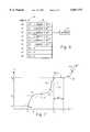
- FIG. 1is a block diagram illustrating a smart temperature sensing device 10 coupled to a field signal acquisition unit (FSAU) 12.
- the smart temperature sensing device 10senses a temperature of its environment and sends an analog electronic signal to the FSAU 12.
- the FSAU 12in turn, converts the electrical signal from the smart sensing device 10 into a value indicative of the temperature of the environment.
- FIG. 2is a schematic diagram illustrating in greater detail the smart temperature sensing device 10 coupled to the FSAU 12.
- the smart temperature sensing device 10comprises a sensor unit 14 including a handle portion 15 and a temperature sensor 16 coupled together via a spacer portion 18.
- the spacer portion 18serves to provide a suitable distance between the handle portion 15 and the temperature sensor 16 under circumstances in which the thermal environment at the temperature sensor portion 16 is substantially hot or cold to protect any plastic materials, electronics, or potting compounds associated with the sensor unit 14 from thermal damage and protect a user's hand on the handle portion 15 from suffering any discomfort.
- the smart temperature sensing device 10could operate without the spacer portion 18 and thereby incorporate the handle portion 15 and the temperature sensor 16 together on or within the same sensor unit 14.
- the smart temperature sensing device 10may further isolate the sensor unit 14 from the temperature sensor 16 by incorporating each into separate housings or subunits, wherein both remain separate from the FSAU 12.
- the smart temperature sensing device 10is coupled to the FSAU 12 through a wire connector 20.
- the FSAU 12includes a display 22, control knobs 24, and conversion circuitry (not shown) which is internal to the FSAU 12 and converts the analog electrical signal from the smart temperature sensing device 10 into a value representative of the temperature at the temperature sensor 16.
- the FSAU 12displays the temperature on the display 22 and the control knobs 24 (which are optional) are used to alter the contrast of the display 22, convert the temperature display from degrees Farenheight to degrees Celsius or alternatively to degrees Kelvin, or provide other control functions.
- the FSAU 12may include additional buttons or other control indicia to effectuate conversion functions.
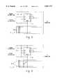
- FIG. 3is a block diagram illustrating the internal circuity of both the smart temperature sensing device 10 and the FSAU 12.
- the smart temperature sensing device 10has a memory 25 and the temperature sensor 16 coupled to a noise suppression circuit 26.
- the memory 25 and the noise suppression circuit 26are connected to the FSAU 12 through a P2 connector 27, which is a common parallel-type connector, which couples the smart temperature sensing device 10 and the FSAU 12 together.
- a different type of connectormay also be utilized such as a bundled wire harness.
- the FSAU 12includes a processor 28 connected to a memory 30, an analog-to-digital converter 32, and the display 22.
- the memory 25 of the smart temperature sensing device 10is coupled to the processor 28 via the P2 connector 27, and the noise suppression circuit 26 is coupled to the analog-to-digital converter 32 as well.
- the memory 25may be located in either the handle portion 15, the spacer portion 18 or the connector 27 where, in each case, the memory 25 is separate from the FSAU 12.
- the smart temperature sensing device 10works in conjunction with the FSAU 12 in the following manner.
- the memory 25 of the smart temperature sensing device 10contains, in one embodiment, historical calibration data that characterizes the nonlinear behavior of a class of sensors over temperature.
- the temperature sensor 16is a thermocouple-type sensor
- the nonlinear historical calibration datarepresents the average nonlinear behavior of many thermocouple-type sensors that have been calibrated in the past.
- the historical calibration datarepresents the average nonlinear behavior for thermocouple-type sensors.
- different nonlinear historical calibration datawill be used for other type temperature sensors 16 such as an RTD-type temperature sensor.
- the memory 25 of the smart temperature sensing device 10contains custom calibration data which uniquely characterizes the nonlinear behavior of the temperature sensor 16. Calibration coefficients are determined and loaded into the memory 25; how this is accomplished will be discussed infra.
- the processor 28Upon initially coupling the smart temperature sensing device 10 to the FSAU 12 (via the P2 connector 27) the processor 28 immediately accesses the memory 25 to download the custom calibration coefficients resident within the memory 25 into the memory 30 of the FSAU 12.
- the temperature sensor 16upon being placed in its respective temperature environment, senses the temperature and outputs an analog electrical signal indicative of the temperature.
- the analog electrical signalpasses through the noise suppression circuit 26, which effectively filters the analog electrical signal, preferably through a band-pass filter arrangement, and eliminates noise associated with the signal.
- the noise suppression circuit 26then passes the filtered electrical signal to the analog-to-digital converter 32 via the P2 connector 27.
- the analog-to-digital converter 32converts the analog filtered electrical signal into a digital signal (or binary word) for the processor 28 which converts, using the custom calibration coefficients now resident within the memory 30, the digital signal into a temperature value which accurately represents the temperature of the environment at the temperature sensor 16.
- the processor 28converts the electrical signal, which is a voltage (EMF) or resistance value, into a temperature through the following algorithm:
- C0, C1 . . . C8represent the custom calibration coefficients and EMF represents the voltage value (typically in millivolts) or resistance value (in ohms).
- the processor 28then displays that temperature value via the display 22.
- the memory 25 within the smart temperature sensing device 10may also contain additional data to provide improved conversion accuracy and system reliability.
- the memory 25may store a time constant associated with the particular temperature sensor 16.
- the time constantrepresents the time it takes for the temperature sensor 16 to respond to a change in temperature.
- the processor 28may use the time constant data in at least two ways: first, if the temperature sensor 16 is sensing the temperature at a number of different temperature interactions, the processor 28 knows how long to wait to convert the signal from the temperature sensor 16 to ensure that the measurement is accurate. Second, if the processor 28 is also controlling the heating or cooling of an oven apparatus, it may use the time constant data in a temperature control algorithm to more precisely control the temperature.
- Additional data within the memory 25may consist of maintenance data regarding maintenance scheduling for the temperature sensor 16. For example, if the temperature sensor 16 should be tested or checked every "X" days, the memory 25 may download "X" to the processor 28 which will begin incrementing a clock. When the clock reaches "X", the processor 28 will communicate to the user via the display 22 that the temperature sensor 28 requires maintenance.
- the data within the memory 25may include data for temperature sensor type ("X" days for RTDs, "Y” days for thermocouples, etc.) or sensor use (replace or repair every "Z” measurement).
- the memory 25may also contain intended use environment data.
- intended use environment dataFor example, temperature sensors 16 experience a known drift when measuring temperatures in a particular environment over time.
- the processor 28may use this intended use environment data to approximately offset measured temperatures in that particular environment over time, thereby accurately taking into account drift within the particular temperature sensor 16. Because drift is a function of the particular environment, the temperature sensor 16 may be uniquely customized for a particular intended use environment.
- Regulatory data specific to a particular customermay also be stored within the memory 25. For example, ISO-9000 specification requirements, internal quality control standards, or UL mandates may require that particular actions be taken at various times to monitor, replace or repair the temperature sensor 16.
- the processor 28downloads this data and provides prompts to the user via the display 22 to ensure that the regulatory requirements are addressed.
- regulatory datamay also include data on the date of the sensor's manufacture, its material lot, when and where it was tested, a serial number or other traceability information.
- Cold junction compensation coefficients for thermocouplesmay also be downloaded into the memory 25.
- a separate sensoris placed at the cold end of the thermocouple junction and the sensor must convert its output into an equivalent thermocouple signal in millivolts to subsequently calculate the temperature at its "hot" end. Since each style thermocouple (type K,C,J or T, for example) has its own unique conversion parameters, a universal conversion algorithm results in inaccuracies. Since each temperature sensor 16 (when using a thermocouple-type sensor) will know the style thermocouple being used, the unique compensation coefficient may be placed within the memory 25 for subsequent use by the processor 28. Therefore, a plethora of data may be placed within the memory 25 which is unique to each temperature sensor 16, thereby providing improved conversion accuracy and sensor reliability.
- FIG. 4illustrates a calibration system 34 having the smart temperature sensing device 10 coupled to a computer 36.
- the calibration system 34is preferably utilized prior to sale of the smart temperature sensing device 10 such that purchase of the smart temperature sensing device 10 will include the custom calibration data already resident within the memory 25.
- the calibration systemoperates by placing the sensor unit 14 in a thermal environment having a known temperature.
- the sensor unit 14outputs an analog signal to the computer 36 simultaneously with a recording of the known temperature by the computer 36.
- the thermal environment temperatureis known to the computer 36 via a signal from a standard sensing device with verified calibration provided from a reference lab such as NIST.
- the calibration system 34increments the temperature of the thermal environment to a second known temperature and repeats the thermal measurement with the smart temperature sensing device 10.
- the calibration system 34repeats the steps until a sufficient number of data points have been collected, whereby the computer 36 then has a number of signal values associated with a number of known temperatures (paired data points).
- the computer 36uses an algorithm to calculate a plurality of calibration coefficients for a polynomial which represents a curve which matches the paired data points.
- FIG. 5is a table which represents the paired data points gathered from the calibration system 34 of FIG. 4.
- FIG. 5has a calibration temperature column 38 which lists a plurality of calibration temperatures; when the calibration system 34 varies the temperature of the environment, that temperature is recorded in the calibration temperature column 38.
- a sensor output column 40lists all the analog voltage signal values or resistance from the smart temperature sensing device 10 gathered during the recordation of the calibration system 34.
- the tablehas a plurality of paired data points, namely the calibration temperature column 38 and the sensor output column 40, wherein an output voltage signal or resistance value is coupled or paired to each respective calibration temperature.
- the computer 36 of the calibration system 34takes the values for the paired data points of calibration temperature column 38 and the sensor output column 40 and uses these paired data points to calculate the calibration coefficients.
- the computer 36utilizes the plurality of paired data points, in a preferred embodiment, in a least squares fitting algorithm to find a polynomial of minimal degree of the form:
- C0,C1, etc.are the calibration coefficients.
- the computer 36downloads the calculated custom calibration coefficients into the memory 25 of the smart temperature sensing device 10 which is illustrated in conjunction with FIG. 6.
- FIG. 6is a block diagram illustrating the computer 36 connected to the memory 25 of the smart temperature sensing device 10.
- a memory address portion 43is located within the memory 25 and represents predetermined, fixed addresses (A0-A8) at which the custom calibration coefficients reside within the memory 25.
- FIG. 7is a graph illustrating a thermocouple-type sensor as an example, having temperature (T) on the X-axis and the signal voltage (V) on the Y-axis.
- Ttemperature
- Vsignal voltage
- FIG. 7is a graph illustrating a thermocouple-type sensor as an example, having temperature (T) on the X-axis and the signal voltage (V) on the Y-axis.
- Ttemperature
- Vsignal voltage
- Y-axisOn the graph is a plurality of paired data points 44 (t 1 ,v 1 ), (t 2 ,v 2 ), etc. collected in the manner described above in conjunction with FIGS. 4 and 5.
- a straight line approximation 45is made using the paired data points. Then, when a voltage signal is received (V 0 ) the corresponding temperature (T L ) on the straight line 45 is determined.
- the temperature sensor 16does not behave in a perfectly linear manner over its temperature range, but rather behaves nonlinearly.
- the voltage signal (V 0 )corresponds to a temperature T 0 which is lower than T L .
- the nonlinear coefficients for the polynomial that characterize the nonlinear voltage-temperature relationship 46eliminate the error ( ⁇ T) associated with prior art linear approximations.
- FIG. 8is a schematic diagram showing in detail the smart temperature sensing device 10 of FIG. 3, namely a resistance temperature device (RTD) 47 coupled to an EEPROM 48.
- the RTD 47 and the EEPROM 48represent a detailed representation of the temperature sensor 16 coupled to the memory 25 within the handle portion 14 (or alternatively a separate subunit) of the smart temperature sensing device 10 of FIGS. 2 and 3.
- the EEPROM 48operates in conjunction with the RTD 47 in the following manner. After the computer 36 has gathered the paired data points and calculated the calibration coefficients associated with the particular probe, which in this case is the RTD 47, and the user wishes to enable the calibration, the user places a jumper between the part enable pin and the power supply which is coupled to the voltage supply pin of the EEPROM 48.
- the chip select pinis driven high (by the computer 36) and the calibration coefficient data is incrementally read in (or clocked) through the D0 and D1 pins.
- the userdisconnects the jumper between the part enable pin up and the power supply and subsequently places the jumper between the part enable pin and the ground pin which disables the downloading of calibration coefficients into the memory 25.
- the processor 28Upon power-up, the processor 28 reads and downloads the calibration coefficients resident within the EEPROM 48 into the memory 30 associated with the FSAU 12. The processor 28 pulls the chip select pin low which enables data to be read from the memory 25. The calibration coefficient data is clocked out of the D0 and D1 pins and stored in the memory 30 for use by the processor 28. In this manner, the EEPROM 48 communicates the custom calibration coefficients to the processor 28 for use in converting analog signals received from the temperature sensor 16.
- the RTD 47in this particular embodiment, senses the temperature by generating the analog signal and communicates that either directly to the analog-to-digital converter 32 or alternatively may send that to the analog-to-digital converter 32 via the noise suppression circuit 26, as illustrated in FIG. 3.
- FIG. 9is a schematic diagram illustrating the EEPROM 48 operating in conjunction with a thermocouple sensor 52.
- the EEPROM 48operates in a similar fashion as described in conjunction with FIG. 7 and operates to enable calibration by clocking in the calibration coefficients from the processor 28. Subsequently the calibration coefficients data resident within the EEPROM 48 can be read out to the memory 30 by the processor 28 for use in accurately calculating the temperature.
Landscapes
- Physics & Mathematics (AREA)
- General Physics & Mathematics (AREA)
- Measuring Temperature Or Quantity Of Heat (AREA)
- Arrangements For Transmission Of Measured Signals (AREA)
Abstract
Description
Claims (21)
Priority Applications (3)
| Application Number | Priority Date | Filing Date | Title |
|---|---|---|---|
| US08/718,921US5857777A (en) | 1996-09-25 | 1996-09-25 | Smart temperature sensing device |
| PCT/US1997/017068WO1998013677A1 (en) | 1996-09-25 | 1997-09-24 | Smart temperature sensing device |
| AU45911/97AAU4591197A (en) | 1996-09-25 | 1997-09-24 | Smart temperature sensing device |
Applications Claiming Priority (1)
| Application Number | Priority Date | Filing Date | Title |
|---|---|---|---|
| US08/718,921US5857777A (en) | 1996-09-25 | 1996-09-25 | Smart temperature sensing device |
Publications (1)
| Publication Number | Publication Date |
|---|---|
| US5857777Atrue US5857777A (en) | 1999-01-12 |
Family
ID=24888102
Family Applications (1)
| Application Number | Title | Priority Date | Filing Date |
|---|---|---|---|
| US08/718,921Expired - LifetimeUS5857777A (en) | 1996-09-25 | 1996-09-25 | Smart temperature sensing device |
Country Status (3)
| Country | Link |
|---|---|
| US (1) | US5857777A (en) |
| AU (1) | AU4591197A (en) |
| WO (1) | WO1998013677A1 (en) |
Cited By (436)
| Publication number | Priority date | Publication date | Assignee | Title |
|---|---|---|---|---|
| US6161958A (en)* | 1997-06-04 | 2000-12-19 | Digital Security Controls Ltd. | Self diagnostic heat detector |
| WO2000079233A1 (en)* | 1999-06-18 | 2000-12-28 | Samba Sensors Ab | A method and a device for bending compensation in intensity-based fibre-optical measuring systems |
| US6167634B1 (en)* | 1998-03-28 | 2001-01-02 | Snu Precision Co., Ltd. | Measurement and compensation system for thermal errors in machine tools |
| US6517240B1 (en)* | 1999-11-05 | 2003-02-11 | Durametrics, Inc. | Ultrasonic thermometer system |
| US20030091090A1 (en)* | 1999-12-24 | 2003-05-15 | Jorg Schieferdecker | Method for the correction of the output signal of an infra red radiation multiple element sensor |
| US6609076B2 (en)* | 2001-09-28 | 2003-08-19 | Claud S. Gordon Company | Interface device and method of use with a smart sensor |
| US20030158683A1 (en)* | 2002-02-19 | 2003-08-21 | Claude Gauthier | Temperature calibration using on-chip electrical fuses |
| US6643610B1 (en)* | 1999-09-24 | 2003-11-04 | Rosemount Inc. | Process transmitter with orthogonal-polynomial fitting |
| US6655835B2 (en)* | 1999-12-21 | 2003-12-02 | Schweitzer Engineering Laboratories Inc. | Setting-free resistive temperature device (RTD) measuring module |
| US20040008752A1 (en)* | 2002-07-15 | 2004-01-15 | Jay Prabhakar | System and method of monitoring temperature |
| US20040013165A1 (en)* | 2001-02-21 | 2004-01-22 | Holger Plote | Method and device for correcting a temperature signal |
| US20040047392A1 (en)* | 2002-09-06 | 2004-03-11 | Shu-Mei Wu | Apparatus for measuring ear and forehead temperature |
| US20040052290A1 (en)* | 2002-05-21 | 2004-03-18 | Kendro Laboratory Product, Lp | Temperature sensor pre-calibration method and apparatus |
| US20040052299A1 (en)* | 2002-07-29 | 2004-03-18 | Jay Paul R. | Temperature correction calibration system and method for optical controllers |
| US20040114659A1 (en)* | 2002-10-11 | 2004-06-17 | Welch Allyn, Inc. | Thermometry probe calibration method |
| US20040135643A1 (en)* | 2003-01-09 | 2004-07-15 | International Business Machines Corporation | Method to calibrate a chip with multiple temperature sensitive ring oscillators by calibrating only TSRO |
| WO2004065896A1 (en)* | 2002-12-20 | 2004-08-05 | Thales | Method and device for magnetic measurement of the position and orientation of a mobile object relative to a fixed structure |
| US20040165646A1 (en)* | 2003-02-20 | 2004-08-26 | Shidemantle Jack P. | Digitally modified resistive output for a temperature sensor |
| US20040170213A1 (en)* | 2003-02-27 | 2004-09-02 | Richard Rund | Food safety thermometer |
| US20040170214A1 (en)* | 2003-02-27 | 2004-09-02 | Richard Rund | Food safety thermometer |
| US20040190585A1 (en)* | 2003-03-27 | 2004-09-30 | International Business Machines Corporation | Method to calibrate a temperature sensitive ring oscillator with minimal test time |
| US6811306B2 (en)* | 1998-09-15 | 2004-11-02 | Jonathan Gerlitz | Infrared ear thermometer |
| US6827488B2 (en) | 2002-10-10 | 2004-12-07 | Welch Allyn, Inc. | Sealed probe chamber for thermometry apparatus |
| US20040252750A1 (en)* | 2003-06-12 | 2004-12-16 | Gruszecki Gary A. | Patient temperature repeating system and method |
| US20050049501A1 (en)* | 1999-09-03 | 2005-03-03 | Conero Ronald S. | Smart physiologic parameter sensor and method |
| US20050052274A1 (en)* | 2003-09-09 | 2005-03-10 | Mattoon Carl V. | Resistive temperature device (RTD) module with improved noise immunity |
| US20050094705A1 (en)* | 2003-11-05 | 2005-05-05 | Microlife Intellectual Property Gmbh | Infrared thermometer and method for determining temperature |
| WO2005057152A1 (en)* | 2003-12-03 | 2005-06-23 | Watlow Electric Manufacturing Company | Sensor drift compensation by lot |
| WO2005073671A1 (en)* | 2004-01-28 | 2005-08-11 | Expert Monitoring Limited | Wireless sensor monitoring systems |
| US20050259517A1 (en)* | 2004-05-10 | 2005-11-24 | Airmar Technology Corporation | Transducer identification |
| US20060045164A1 (en)* | 2004-08-31 | 2006-03-02 | Schuh William C | System and method of compensation for device mounting and thermal transfer error |
| US20060079792A1 (en)* | 2004-10-07 | 2006-04-13 | Finburgh Simon E | Compact apparatus and methods for non-invasively measuring hemodynamic parameters |
| US20060123915A1 (en)* | 2004-12-14 | 2006-06-15 | Helix Technology Corporation | Method and apparatus for storing vacuum gauge calibration parameters and measurement data on a vacuum gauge structure |
| US20060153276A1 (en)* | 2004-12-07 | 2006-07-13 | Jens Hartmann | Temperature measuring system and method |
| US20060222048A1 (en)* | 1997-06-24 | 2006-10-05 | Francesco Pompei | Ambient and perfusion normalized temperature detector |
| US20070083088A1 (en)* | 2003-09-12 | 2007-04-12 | Laborie Medical Technologies Inc. | Apparatus and method for medical measurement |
| US7223014B2 (en) | 2003-03-28 | 2007-05-29 | Intempco Controls Ltd. | Remotely programmable integrated sensor transmitter |
| US20070179400A1 (en)* | 2002-07-12 | 2007-08-02 | Laborie Medical Technologies, Inc. | Apparatus and Method for Medical Measurement |
| US7309157B1 (en)* | 2004-09-28 | 2007-12-18 | National Semiconductor Corporation | Apparatus and method for calibration of a temperature sensor |
| US20080053242A1 (en)* | 2006-08-29 | 2008-03-06 | Schumacher Mark S | Process device with density measurement |
| WO2008116069A1 (en)* | 2007-03-22 | 2008-09-25 | Baker Hughes Incorporated | Location dependent calibration for distributed temperature sensor measurements |
| US7461974B1 (en) | 2004-06-09 | 2008-12-09 | National Semiconductor Corporation | Beta variation cancellation in temperature sensors |
| US20090010302A1 (en)* | 2006-03-01 | 2009-01-08 | E.G.O. Elektro-Geraetebau Gmbh | Method and device for identifying a temperature sensor connected to a control unit |
| US20090027659A1 (en)* | 1999-06-18 | 2009-01-29 | Sambra Sensors Ab | Measuring system for measuring a physical parameter influencing a sensor element |
| US20090041086A1 (en)* | 2007-08-09 | 2009-02-12 | The Edward Orton, Jr. Ceramic Foundation | Furnace temperature monitoring device and method |
| US20090052498A1 (en)* | 2007-08-24 | 2009-02-26 | Asm America, Inc. | Thermocouple |
| US20090080490A1 (en)* | 2007-09-21 | 2009-03-26 | Siemens Energy & Automation, Inc. | Systems, Devices, and/or Methods for Managing a Thermocouple Module |
| US20090201972A1 (en)* | 2005-12-23 | 2009-08-13 | Endress + Hauser Gmbh + Co.Kg | Sensor System for Determining a Physical Measured Variable |
| US20090292484A1 (en)* | 2008-05-23 | 2009-11-26 | Wiklund David E | Multivariable process fluid flow device with energy flow calculation |
| US20100128753A1 (en)* | 2008-11-26 | 2010-05-27 | Rubbermaid Incorporated | Multiple-Stage Thermometer and Temperature Monitoring |
| US20100161270A1 (en)* | 2008-12-18 | 2010-06-24 | Vijit Paul Jayasheela | Method For Processing A Temperature Sensor Signal |
| US20100286842A1 (en)* | 2009-05-06 | 2010-11-11 | Asm America, Inc. | Smart Temperature Measuring Device |
| US20110010035A1 (en)* | 2009-07-13 | 2011-01-13 | Ford Global Technologies, Llc | Smart vehicle sensor |
| US20110090935A1 (en)* | 2009-10-16 | 2011-04-21 | John Michael Cuffe | Method for performing ultrasonic testing |
| US20110158283A1 (en)* | 2009-12-31 | 2011-06-30 | Welch Allyn, Inc. | Temperature-measurement probe |
| US20110224940A1 (en)* | 2010-03-09 | 2011-09-15 | Howe Spencer K | Temperature Prediction Transmitter |
| US20120065923A1 (en)* | 2010-09-14 | 2012-03-15 | General Electric Company | Integrated cold junction compensation circuit for thermocouple connections |
| US20120065540A1 (en)* | 2010-09-12 | 2012-03-15 | Medisim Ltd | Temperature sensor with calibrated analog resistive output |
| WO2012119829A1 (en)* | 2011-03-04 | 2012-09-13 | Endress+Hauser Wetzer Gmbh+Co. Kg | Measuring device with compensation for a delayed response behavior |
| CN102879121A (en)* | 2012-09-13 | 2013-01-16 | 北京百纳威尔科技有限公司 | Temperature measuring method and communication equipment |
| US8449173B1 (en)* | 2008-04-10 | 2013-05-28 | Google Inc. | Method and system for thermal testing of computing system components |
| US8616765B2 (en) | 2008-12-08 | 2013-12-31 | Asm America, Inc. | Thermocouple |
| CN103698056A (en)* | 2013-12-16 | 2014-04-02 | 杭州华安医疗保健用品有限公司 | Calibrated temperature error correction device and correction method |
| USD702188S1 (en) | 2013-03-08 | 2014-04-08 | Asm Ip Holding B.V. | Thermocouple |
| CN104048777A (en)* | 2014-06-24 | 2014-09-17 | 中国东方电气集团有限公司 | Temperature value and resistance value conversion method for NTC-type thermistor |
| WO2014153035A1 (en)* | 2013-03-14 | 2014-09-25 | Primex Wireless, Inc. | Method and apparatus for probe calibration |
| CN105092095A (en)* | 2014-05-04 | 2015-11-25 | 睿励科学仪器(上海)有限公司 | Temperature calibrating method and device |
| US9267850B2 (en) | 2009-05-06 | 2016-02-23 | Asm America, Inc. | Thermocouple assembly with guarded thermocouple junction |
| US20160377489A1 (en)* | 2015-06-24 | 2016-12-29 | Lsis Co., Ltd. | Method for temperature drift compensation of temperature measurement device using thermocouple |
| US9599521B2 (en) | 2014-01-27 | 2017-03-21 | Medisim, Ltd. | Interface between vital-signs sensors and patient monitor |
| US9947184B2 (en)* | 2016-04-11 | 2018-04-17 | Verizon Patent And Licensing, Inc. | Enabling interchangeability of sensor devices associated with a user device |
| CN109283955A (en)* | 2018-09-20 | 2019-01-29 | 广东美的暖通设备有限公司 | The control method and household electrical appliance of temperature sampling |
| US10229833B2 (en) | 2016-11-01 | 2019-03-12 | Asm Ip Holding B.V. | Methods for forming a transition metal nitride film on a substrate by atomic layer deposition and related semiconductor device structures |
| US10249577B2 (en) | 2016-05-17 | 2019-04-02 | Asm Ip Holding B.V. | Method of forming metal interconnection and method of fabricating semiconductor apparatus using the method |
| US10249524B2 (en) | 2017-08-09 | 2019-04-02 | Asm Ip Holding B.V. | Cassette holder assembly for a substrate cassette and holding member for use in such assembly |
| US10262859B2 (en) | 2016-03-24 | 2019-04-16 | Asm Ip Holding B.V. | Process for forming a film on a substrate using multi-port injection assemblies |
| US10269558B2 (en) | 2016-12-22 | 2019-04-23 | Asm Ip Holding B.V. | Method of forming a structure on a substrate |
| US10276355B2 (en) | 2015-03-12 | 2019-04-30 | Asm Ip Holding B.V. | Multi-zone reactor, system including the reactor, and method of using the same |
| US10283353B2 (en) | 2017-03-29 | 2019-05-07 | Asm Ip Holding B.V. | Method of reforming insulating film deposited on substrate with recess pattern |
| US10290508B1 (en) | 2017-12-05 | 2019-05-14 | Asm Ip Holding B.V. | Method for forming vertical spacers for spacer-defined patterning |
| US10285598B2 (en) | 2006-05-13 | 2019-05-14 | United States Gtm Medical Devices | Continuous positioning apparatus and methods |
| US10312129B2 (en) | 2015-09-29 | 2019-06-04 | Asm Ip Holding B.V. | Variable adjustment for precise matching of multiple chamber cavity housings |
| US10312055B2 (en) | 2017-07-26 | 2019-06-04 | Asm Ip Holding B.V. | Method of depositing film by PEALD using negative bias |
| US10319588B2 (en) | 2017-10-10 | 2019-06-11 | Asm Ip Holding B.V. | Method for depositing a metal chalcogenide on a substrate by cyclical deposition |
| US10322384B2 (en) | 2015-11-09 | 2019-06-18 | Asm Ip Holding B.V. | Counter flow mixer for process chamber |
| US10340125B2 (en) | 2013-03-08 | 2019-07-02 | Asm Ip Holding B.V. | Pulsed remote plasma method and system |
| US10340135B2 (en) | 2016-11-28 | 2019-07-02 | Asm Ip Holding B.V. | Method of topologically restricted plasma-enhanced cyclic deposition of silicon or metal nitride |
| US10335081B2 (en) | 2002-01-30 | 2019-07-02 | United States Gtm Medical Devices | Apparatus and method for interfacing time-variant signals |
| US10343920B2 (en) | 2016-03-18 | 2019-07-09 | Asm Ip Holding B.V. | Aligned carbon nanotubes |
| US10361201B2 (en) | 2013-09-27 | 2019-07-23 | Asm Ip Holding B.V. | Semiconductor structure and device formed using selective epitaxial process |
| US10367080B2 (en) | 2016-05-02 | 2019-07-30 | Asm Ip Holding B.V. | Method of forming a germanium oxynitride film |
| US10364493B2 (en) | 2016-08-25 | 2019-07-30 | Asm Ip Holding B.V. | Exhaust apparatus and substrate processing apparatus having an exhaust line with a first ring having at least one hole on a lateral side thereof placed in the exhaust line |
| US10364496B2 (en) | 2011-06-27 | 2019-07-30 | Asm Ip Holding B.V. | Dual section module having shared and unshared mass flow controllers |
| US10366864B2 (en) | 2013-03-08 | 2019-07-30 | Asm Ip Holding B.V. | Method and system for in-situ formation of intermediate reactive species |
| US10378106B2 (en) | 2008-11-14 | 2019-08-13 | Asm Ip Holding B.V. | Method of forming insulation film by modified PEALD |
| US10381219B1 (en) | 2018-10-25 | 2019-08-13 | Asm Ip Holding B.V. | Methods for forming a silicon nitride film |
| US10381226B2 (en) | 2016-07-27 | 2019-08-13 | Asm Ip Holding B.V. | Method of processing substrate |
| US10388513B1 (en) | 2018-07-03 | 2019-08-20 | Asm Ip Holding B.V. | Method for depositing silicon-free carbon-containing film as gap-fill layer by pulse plasma-assisted deposition |
| US10388509B2 (en) | 2016-06-28 | 2019-08-20 | Asm Ip Holding B.V. | Formation of epitaxial layers via dislocation filtering |
| US10395919B2 (en) | 2016-07-28 | 2019-08-27 | Asm Ip Holding B.V. | Method and apparatus for filling a gap |
| US10403504B2 (en) | 2017-10-05 | 2019-09-03 | Asm Ip Holding B.V. | Method for selectively depositing a metallic film on a substrate |
| US10410943B2 (en) | 2016-10-13 | 2019-09-10 | Asm Ip Holding B.V. | Method for passivating a surface of a semiconductor and related systems |
| WO2019191639A1 (en) | 2018-03-29 | 2019-10-03 | Cooper-Atkins Corporation | Systems and methods for smart thermocouple temperature probe |
| US10435790B2 (en) | 2016-11-01 | 2019-10-08 | Asm Ip Holding B.V. | Method of subatmospheric plasma-enhanced ALD using capacitively coupled electrodes with narrow gap |
| US10438965B2 (en) | 2014-12-22 | 2019-10-08 | Asm Ip Holding B.V. | Semiconductor device and manufacturing method thereof |
| US10446393B2 (en) | 2017-05-08 | 2019-10-15 | Asm Ip Holding B.V. | Methods for forming silicon-containing epitaxial layers and related semiconductor device structures |
| US10458018B2 (en) | 2015-06-26 | 2019-10-29 | Asm Ip Holding B.V. | Structures including metal carbide material, devices including the structures, and methods of forming same |
| US10468261B2 (en) | 2017-02-15 | 2019-11-05 | Asm Ip Holding B.V. | Methods for forming a metallic film on a substrate by cyclical deposition and related semiconductor device structures |
| US10468251B2 (en) | 2016-02-19 | 2019-11-05 | Asm Ip Holding B.V. | Method for forming spacers using silicon nitride film for spacer-defined multiple patterning |
| US10483099B1 (en) | 2018-07-26 | 2019-11-19 | Asm Ip Holding B.V. | Method for forming thermally stable organosilicon polymer film |
| US10480072B2 (en) | 2009-04-06 | 2019-11-19 | Asm Ip Holding B.V. | Semiconductor processing reactor and components thereof |
| US10504742B2 (en) | 2017-05-31 | 2019-12-10 | Asm Ip Holding B.V. | Method of atomic layer etching using hydrogen plasma |
| US10501866B2 (en) | 2016-03-09 | 2019-12-10 | Asm Ip Holding B.V. | Gas distribution apparatus for improved film uniformity in an epitaxial system |
| US10510536B2 (en) | 2018-03-29 | 2019-12-17 | Asm Ip Holding B.V. | Method of depositing a co-doped polysilicon film on a surface of a substrate within a reaction chamber |
| US10529563B2 (en) | 2017-03-29 | 2020-01-07 | Asm Ip Holdings B.V. | Method for forming doped metal oxide films on a substrate by cyclical deposition and related semiconductor device structures |
| US10529542B2 (en) | 2015-03-11 | 2020-01-07 | Asm Ip Holdings B.V. | Cross-flow reactor and method |
| US10529554B2 (en) | 2016-02-19 | 2020-01-07 | Asm Ip Holding B.V. | Method for forming silicon nitride film selectively on sidewalls or flat surfaces of trenches |
| US10535516B2 (en) | 2018-02-01 | 2020-01-14 | Asm Ip Holdings B.V. | Method for depositing a semiconductor structure on a surface of a substrate and related semiconductor structures |
| US10541173B2 (en) | 2016-07-08 | 2020-01-21 | Asm Ip Holding B.V. | Selective deposition method to form air gaps |
| US10541333B2 (en) | 2017-07-19 | 2020-01-21 | Asm Ip Holding B.V. | Method for depositing a group IV semiconductor and related semiconductor device structures |
| US10559458B1 (en) | 2018-11-26 | 2020-02-11 | Asm Ip Holding B.V. | Method of forming oxynitride film |
| US10566223B2 (en) | 2012-08-28 | 2020-02-18 | Asm Ip Holdings B.V. | Systems and methods for dynamic semiconductor process scheduling |
| US10561975B2 (en) | 2014-10-07 | 2020-02-18 | Asm Ip Holdings B.V. | Variable conductance gas distribution apparatus and method |
| DE102018121051A1 (en)* | 2018-08-29 | 2020-03-05 | SIKA Dr. Siebert & Kühn GmbH & Co. KG | Method for calibrating a temperature measuring device |
| US10590535B2 (en) | 2017-07-26 | 2020-03-17 | Asm Ip Holdings B.V. | Chemical treatment, deposition and/or infiltration apparatus and method for using the same |
| US10600673B2 (en) | 2015-07-07 | 2020-03-24 | Asm Ip Holding B.V. | Magnetic susceptor to baseplate seal |
| US10607895B2 (en) | 2017-09-18 | 2020-03-31 | Asm Ip Holdings B.V. | Method for forming a semiconductor device structure comprising a gate fill metal |
| US10604847B2 (en) | 2014-03-18 | 2020-03-31 | Asm Ip Holding B.V. | Gas distribution system, reactor including the system, and methods of using the same |
| US10605530B2 (en) | 2017-07-26 | 2020-03-31 | Asm Ip Holding B.V. | Assembly of a liner and a flange for a vertical furnace as well as the liner and the vertical furnace |
| USD880437S1 (en) | 2018-02-01 | 2020-04-07 | Asm Ip Holding B.V. | Gas supply plate for semiconductor manufacturing apparatus |
| US10612137B2 (en) | 2016-07-08 | 2020-04-07 | Asm Ip Holdings B.V. | Organic reactants for atomic layer deposition |
| US10612136B2 (en) | 2018-06-29 | 2020-04-07 | ASM IP Holding, B.V. | Temperature-controlled flange and reactor system including same |
| US10622375B2 (en) | 2016-11-07 | 2020-04-14 | Asm Ip Holding B.V. | Method of processing a substrate and a device manufactured by using the method |
| US10643826B2 (en) | 2016-10-26 | 2020-05-05 | Asm Ip Holdings B.V. | Methods for thermally calibrating reaction chambers |
| US10643904B2 (en) | 2016-11-01 | 2020-05-05 | Asm Ip Holdings B.V. | Methods for forming a semiconductor device and related semiconductor device structures |
| US10658181B2 (en) | 2018-02-20 | 2020-05-19 | Asm Ip Holding B.V. | Method of spacer-defined direct patterning in semiconductor fabrication |
| US10658205B2 (en) | 2017-09-28 | 2020-05-19 | Asm Ip Holdings B.V. | Chemical dispensing apparatus and methods for dispensing a chemical to a reaction chamber |
| US10655221B2 (en) | 2017-02-09 | 2020-05-19 | Asm Ip Holding B.V. | Method for depositing oxide film by thermal ALD and PEALD |
| US10665452B2 (en) | 2016-05-02 | 2020-05-26 | Asm Ip Holdings B.V. | Source/drain performance through conformal solid state doping |
| US10677621B1 (en) | 2017-09-20 | 2020-06-09 | Continental Control Systems Llc | Sensor apparatus for two-wire sensor measurement and information read-out system |
| US10685834B2 (en) | 2017-07-05 | 2020-06-16 | Asm Ip Holdings B.V. | Methods for forming a silicon germanium tin layer and related semiconductor device structures |
| US10683571B2 (en) | 2014-02-25 | 2020-06-16 | Asm Ip Holding B.V. | Gas supply manifold and method of supplying gases to chamber using same |
| US10692741B2 (en) | 2017-08-08 | 2020-06-23 | Asm Ip Holdings B.V. | Radiation shield |
| US10707106B2 (en) | 2011-06-06 | 2020-07-07 | Asm Ip Holding B.V. | High-throughput semiconductor-processing apparatus equipped with multiple dual-chamber modules |
| US10714315B2 (en) | 2012-10-12 | 2020-07-14 | Asm Ip Holdings B.V. | Semiconductor reaction chamber showerhead |
| US10714385B2 (en) | 2016-07-19 | 2020-07-14 | Asm Ip Holding B.V. | Selective deposition of tungsten |
| US10714350B2 (en) | 2016-11-01 | 2020-07-14 | ASM IP Holdings, B.V. | Methods for forming a transition metal niobium nitride film on a substrate by atomic layer deposition and related semiconductor device structures |
| US10714335B2 (en) | 2017-04-25 | 2020-07-14 | Asm Ip Holding B.V. | Method of depositing thin film and method of manufacturing semiconductor device |
| US10734244B2 (en) | 2017-11-16 | 2020-08-04 | Asm Ip Holding B.V. | Method of processing a substrate and a device manufactured by the same |
| US10734497B2 (en) | 2017-07-18 | 2020-08-04 | Asm Ip Holding B.V. | Methods for forming a semiconductor device structure and related semiconductor device structures |
| US10731249B2 (en) | 2018-02-15 | 2020-08-04 | Asm Ip Holding B.V. | Method of forming a transition metal containing film on a substrate by a cyclical deposition process, a method for supplying a transition metal halide compound to a reaction chamber, and related vapor deposition apparatus |
| US10741385B2 (en) | 2016-07-28 | 2020-08-11 | Asm Ip Holding B.V. | Method and apparatus for filling a gap |
| US10755922B2 (en) | 2018-07-03 | 2020-08-25 | Asm Ip Holding B.V. | Method for depositing silicon-free carbon-containing film as gap-fill layer by pulse plasma-assisted deposition |
| US10770286B2 (en) | 2017-05-08 | 2020-09-08 | Asm Ip Holdings B.V. | Methods for selectively forming a silicon nitride film on a substrate and related semiconductor device structures |
| US10767789B2 (en) | 2018-07-16 | 2020-09-08 | Asm Ip Holding B.V. | Diaphragm valves, valve components, and methods for forming valve components |
| US10770336B2 (en) | 2017-08-08 | 2020-09-08 | Asm Ip Holding B.V. | Substrate lift mechanism and reactor including same |
| US10787741B2 (en) | 2014-08-21 | 2020-09-29 | Asm Ip Holding B.V. | Method and system for in situ formation of gas-phase compounds |
| US10797133B2 (en) | 2018-06-21 | 2020-10-06 | Asm Ip Holding B.V. | Method for depositing a phosphorus doped silicon arsenide film and related semiconductor device structures |
| US10804098B2 (en) | 2009-08-14 | 2020-10-13 | Asm Ip Holding B.V. | Systems and methods for thin-film deposition of metal oxides using excited nitrogen-oxygen species |
| US10811256B2 (en) | 2018-10-16 | 2020-10-20 | Asm Ip Holding B.V. | Method for etching a carbon-containing feature |
| US10818758B2 (en) | 2018-11-16 | 2020-10-27 | Asm Ip Holding B.V. | Methods for forming a metal silicate film on a substrate in a reaction chamber and related semiconductor device structures |
| USD900036S1 (en) | 2017-08-24 | 2020-10-27 | Asm Ip Holding B.V. | Heater electrical connector and adapter |
| US10832903B2 (en) | 2011-10-28 | 2020-11-10 | Asm Ip Holding B.V. | Process feed management for semiconductor substrate processing |
| US10829852B2 (en) | 2018-08-16 | 2020-11-10 | Asm Ip Holding B.V. | Gas distribution device for a wafer processing apparatus |
| US10844484B2 (en) | 2017-09-22 | 2020-11-24 | Asm Ip Holding B.V. | Apparatus for dispensing a vapor phase reactant to a reaction chamber and related methods |
| US10847366B2 (en) | 2018-11-16 | 2020-11-24 | Asm Ip Holding B.V. | Methods for depositing a transition metal chalcogenide film on a substrate by a cyclical deposition process |
| US10847371B2 (en) | 2018-03-27 | 2020-11-24 | Asm Ip Holding B.V. | Method of forming an electrode on a substrate and a semiconductor device structure including an electrode |
| US10847365B2 (en) | 2018-10-11 | 2020-11-24 | Asm Ip Holding B.V. | Method of forming conformal silicon carbide film by cyclic CVD |
| USD903477S1 (en) | 2018-01-24 | 2020-12-01 | Asm Ip Holdings B.V. | Metal clamp |
| US10854498B2 (en) | 2011-07-15 | 2020-12-01 | Asm Ip Holding B.V. | Wafer-supporting device and method for producing same |
| US10851456B2 (en) | 2016-04-21 | 2020-12-01 | Asm Ip Holding B.V. | Deposition of metal borides |
| US10858737B2 (en) | 2014-07-28 | 2020-12-08 | Asm Ip Holding B.V. | Showerhead assembly and components thereof |
| US10867788B2 (en) | 2016-12-28 | 2020-12-15 | Asm Ip Holding B.V. | Method of forming a structure on a substrate |
| US10865475B2 (en) | 2016-04-21 | 2020-12-15 | Asm Ip Holding B.V. | Deposition of metal borides and silicides |
| US10867786B2 (en) | 2018-03-30 | 2020-12-15 | Asm Ip Holding B.V. | Substrate processing method |
| US10872771B2 (en) | 2018-01-16 | 2020-12-22 | Asm Ip Holding B. V. | Method for depositing a material film on a substrate within a reaction chamber by a cyclical deposition process and related device structures |
| US10883175B2 (en) | 2018-08-09 | 2021-01-05 | Asm Ip Holding B.V. | Vertical furnace for processing substrates and a liner for use therein |
| US10886123B2 (en) | 2017-06-02 | 2021-01-05 | Asm Ip Holding B.V. | Methods for forming low temperature semiconductor layers and related semiconductor device structures |
| US20210003461A1 (en)* | 2018-03-22 | 2021-01-07 | University Of Helsinki | Sensor calibration |
| US10892156B2 (en) | 2017-05-08 | 2021-01-12 | Asm Ip Holding B.V. | Methods for forming a silicon nitride film on a substrate and related semiconductor device structures |
| US10896820B2 (en) | 2018-02-14 | 2021-01-19 | Asm Ip Holding B.V. | Method for depositing a ruthenium-containing film on a substrate by a cyclical deposition process |
| US10910262B2 (en) | 2017-11-16 | 2021-02-02 | Asm Ip Holding B.V. | Method of selectively depositing a capping layer structure on a semiconductor device structure |
| US10914004B2 (en) | 2018-06-29 | 2021-02-09 | Asm Ip Holding B.V. | Thin-film deposition method and manufacturing method of semiconductor device |
| US10923344B2 (en) | 2017-10-30 | 2021-02-16 | Asm Ip Holding B.V. | Methods for forming a semiconductor structure and related semiconductor structures |
| US10928731B2 (en) | 2017-09-21 | 2021-02-23 | Asm Ip Holding B.V. | Method of sequential infiltration synthesis treatment of infiltrateable material and structures and devices formed using same |
| US10934619B2 (en) | 2016-11-15 | 2021-03-02 | Asm Ip Holding B.V. | Gas supply unit and substrate processing apparatus including the gas supply unit |
| US10941490B2 (en) | 2014-10-07 | 2021-03-09 | Asm Ip Holding B.V. | Multiple temperature range susceptor, assembly, reactor and system including the susceptor, and methods of using the same |
| US10952675B2 (en) | 2007-10-12 | 2021-03-23 | Shangyi Medical Technology (Hangzhou) Co., Ltd | Apparatus and methods for non-invasively measuring a patient's arterial blood pressure |
| US10975470B2 (en) | 2018-02-23 | 2021-04-13 | Asm Ip Holding B.V. | Apparatus for detecting or monitoring for a chemical precursor in a high temperature environment |
| US11001925B2 (en) | 2016-12-19 | 2021-05-11 | Asm Ip Holding B.V. | Substrate processing apparatus |
| CN112816101A (en)* | 2021-02-20 | 2021-05-18 | 河南中烟工业有限责任公司 | Drum temperature calibration device based on high-temperature battery power supply |
| US11018002B2 (en) | 2017-07-19 | 2021-05-25 | Asm Ip Holding B.V. | Method for selectively depositing a Group IV semiconductor and related semiconductor device structures |
| US11015245B2 (en) | 2014-03-19 | 2021-05-25 | Asm Ip Holding B.V. | Gas-phase reactor and system having exhaust plenum and components thereof |
| US11018047B2 (en) | 2018-01-25 | 2021-05-25 | Asm Ip Holding B.V. | Hybrid lift pin |
| US11022879B2 (en) | 2017-11-24 | 2021-06-01 | Asm Ip Holding B.V. | Method of forming an enhanced unexposed photoresist layer |
| US11024523B2 (en) | 2018-09-11 | 2021-06-01 | Asm Ip Holding B.V. | Substrate processing apparatus and method |
| US11031242B2 (en) | 2018-11-07 | 2021-06-08 | Asm Ip Holding B.V. | Methods for depositing a boron doped silicon germanium film |
| USD922229S1 (en) | 2019-06-05 | 2021-06-15 | Asm Ip Holding B.V. | Device for controlling a temperature of a gas supply unit |
| US11049751B2 (en) | 2018-09-14 | 2021-06-29 | Asm Ip Holding B.V. | Cassette supply system to store and handle cassettes and processing apparatus equipped therewith |
| US11053591B2 (en) | 2018-08-06 | 2021-07-06 | Asm Ip Holding B.V. | Multi-port gas injection system and reactor system including same |
| US11056567B2 (en) | 2018-05-11 | 2021-07-06 | Asm Ip Holding B.V. | Method of forming a doped metal carbide film on a substrate and related semiconductor device structures |
| US11056344B2 (en) | 2017-08-30 | 2021-07-06 | Asm Ip Holding B.V. | Layer forming method |
| US11069510B2 (en) | 2017-08-30 | 2021-07-20 | Asm Ip Holding B.V. | Substrate processing apparatus |
| US11081345B2 (en) | 2018-02-06 | 2021-08-03 | Asm Ip Holding B.V. | Method of post-deposition treatment for silicon oxide film |
| US11088002B2 (en) | 2018-03-29 | 2021-08-10 | Asm Ip Holding B.V. | Substrate rack and a substrate processing system and method |
| US11087997B2 (en) | 2018-10-31 | 2021-08-10 | Asm Ip Holding B.V. | Substrate processing apparatus for processing substrates |
| US11114294B2 (en) | 2019-03-08 | 2021-09-07 | Asm Ip Holding B.V. | Structure including SiOC layer and method of forming same |
| US11114283B2 (en) | 2018-03-16 | 2021-09-07 | Asm Ip Holding B.V. | Reactor, system including the reactor, and methods of manufacturing and using same |
| USD930782S1 (en) | 2019-08-22 | 2021-09-14 | Asm Ip Holding B.V. | Gas distributor |
| US11127589B2 (en) | 2019-02-01 | 2021-09-21 | Asm Ip Holding B.V. | Method of topology-selective film formation of silicon oxide |
| US11127617B2 (en) | 2017-11-27 | 2021-09-21 | Asm Ip Holding B.V. | Storage device for storing wafer cassettes for use with a batch furnace |
| USD931978S1 (en) | 2019-06-27 | 2021-09-28 | Asm Ip Holding B.V. | Showerhead vacuum transport |
| US11139191B2 (en) | 2017-08-09 | 2021-10-05 | Asm Ip Holding B.V. | Storage apparatus for storing cassettes for substrates and processing apparatus equipped therewith |
| US11139308B2 (en) | 2015-12-29 | 2021-10-05 | Asm Ip Holding B.V. | Atomic layer deposition of III-V compounds to form V-NAND devices |
| US11158513B2 (en) | 2018-12-13 | 2021-10-26 | Asm Ip Holding B.V. | Methods for forming a rhenium-containing film on a substrate by a cyclical deposition process and related semiconductor device structures |
| US11171025B2 (en) | 2019-01-22 | 2021-11-09 | Asm Ip Holding B.V. | Substrate processing device |
| USD935572S1 (en) | 2019-05-24 | 2021-11-09 | Asm Ip Holding B.V. | Gas channel plate |
| US11205585B2 (en) | 2016-07-28 | 2021-12-21 | Asm Ip Holding B.V. | Substrate processing apparatus and method of operating the same |
| US11217444B2 (en) | 2018-11-30 | 2022-01-04 | Asm Ip Holding B.V. | Method for forming an ultraviolet radiation responsive metal oxide-containing film |
| US11222772B2 (en) | 2016-12-14 | 2022-01-11 | Asm Ip Holding B.V. | Substrate processing apparatus |
| USD940837S1 (en) | 2019-08-22 | 2022-01-11 | Asm Ip Holding B.V. | Electrode |
| US11227782B2 (en) | 2019-07-31 | 2022-01-18 | Asm Ip Holding B.V. | Vertical batch furnace assembly |
| US11227789B2 (en) | 2019-02-20 | 2022-01-18 | Asm Ip Holding B.V. | Method and apparatus for filling a recess formed within a substrate surface |
| US11233133B2 (en) | 2015-10-21 | 2022-01-25 | Asm Ip Holding B.V. | NbMC layers |
| US11232963B2 (en) | 2018-10-03 | 2022-01-25 | Asm Ip Holding B.V. | Substrate processing apparatus and method |
| US11230766B2 (en) | 2018-03-29 | 2022-01-25 | Asm Ip Holding B.V. | Substrate processing apparatus and method |
| US11251040B2 (en) | 2019-02-20 | 2022-02-15 | Asm Ip Holding B.V. | Cyclical deposition method including treatment step and apparatus for same |
| US11251068B2 (en) | 2018-10-19 | 2022-02-15 | Asm Ip Holding B.V. | Substrate processing apparatus and substrate processing method |
| USD944946S1 (en) | 2019-06-14 | 2022-03-01 | Asm Ip Holding B.V. | Shower plate |
| US11270899B2 (en) | 2018-06-04 | 2022-03-08 | Asm Ip Holding B.V. | Wafer handling chamber with moisture reduction |
| US11274369B2 (en) | 2018-09-11 | 2022-03-15 | Asm Ip Holding B.V. | Thin film deposition method |
| US11282698B2 (en) | 2019-07-19 | 2022-03-22 | Asm Ip Holding B.V. | Method of forming topology-controlled amorphous carbon polymer film |
| US11286562B2 (en) | 2018-06-08 | 2022-03-29 | Asm Ip Holding B.V. | Gas-phase chemical reactor and method of using same |
| US11286558B2 (en) | 2019-08-23 | 2022-03-29 | Asm Ip Holding B.V. | Methods for depositing a molybdenum nitride film on a surface of a substrate by a cyclical deposition process and related semiconductor device structures including a molybdenum nitride film |
| US11289326B2 (en) | 2019-05-07 | 2022-03-29 | Asm Ip Holding B.V. | Method for reforming amorphous carbon polymer film |
| USD947913S1 (en) | 2019-05-17 | 2022-04-05 | Asm Ip Holding B.V. | Susceptor shaft |
| US11295980B2 (en) | 2017-08-30 | 2022-04-05 | Asm Ip Holding B.V. | Methods for depositing a molybdenum metal film over a dielectric surface of a substrate by a cyclical deposition process and related semiconductor device structures |
| USD948463S1 (en) | 2018-10-24 | 2022-04-12 | Asm Ip Holding B.V. | Susceptor for semiconductor substrate supporting apparatus |
| USD949319S1 (en) | 2019-08-22 | 2022-04-19 | Asm Ip Holding B.V. | Exhaust duct |
| US11306395B2 (en) | 2017-06-28 | 2022-04-19 | Asm Ip Holding B.V. | Methods for depositing a transition metal nitride film on a substrate by atomic layer deposition and related deposition apparatus |
| US11315794B2 (en) | 2019-10-21 | 2022-04-26 | Asm Ip Holding B.V. | Apparatus and methods for selectively etching films |
| US11339476B2 (en) | 2019-10-08 | 2022-05-24 | Asm Ip Holding B.V. | Substrate processing device having connection plates, substrate processing method |
| US11342216B2 (en) | 2019-02-20 | 2022-05-24 | Asm Ip Holding B.V. | Cyclical deposition method and apparatus for filling a recess formed within a substrate surface |
| US11345999B2 (en) | 2019-06-06 | 2022-05-31 | Asm Ip Holding B.V. | Method of using a gas-phase reactor system including analyzing exhausted gas |
| US11355338B2 (en) | 2019-05-10 | 2022-06-07 | Asm Ip Holding B.V. | Method of depositing material onto a surface and structure formed according to the method |
| CN114599949A (en)* | 2019-09-20 | 2022-06-07 | 光子控制器有限公司 | Calibration system for fiber optic temperature probe |
| US11361990B2 (en) | 2018-05-28 | 2022-06-14 | Asm Ip Holding B.V. | Substrate processing method and device manufactured by using the same |
| US11374112B2 (en) | 2017-07-19 | 2022-06-28 | Asm Ip Holding B.V. | Method for depositing a group IV semiconductor and related semiconductor device structures |
| US11378337B2 (en) | 2019-03-28 | 2022-07-05 | Asm Ip Holding B.V. | Door opener and substrate processing apparatus provided therewith |
| US11393690B2 (en) | 2018-01-19 | 2022-07-19 | Asm Ip Holding B.V. | Deposition method |
| US11390945B2 (en) | 2019-07-03 | 2022-07-19 | Asm Ip Holding B.V. | Temperature control assembly for substrate processing apparatus and method of using same |
| US11390946B2 (en) | 2019-01-17 | 2022-07-19 | Asm Ip Holding B.V. | Methods of forming a transition metal containing film on a substrate by a cyclical deposition process |
| US11401605B2 (en) | 2019-11-26 | 2022-08-02 | Asm Ip Holding B.V. | Substrate processing apparatus |
| US11414760B2 (en) | 2018-10-08 | 2022-08-16 | Asm Ip Holding B.V. | Substrate support unit, thin film deposition apparatus including the same, and substrate processing apparatus including the same |
| US11424119B2 (en) | 2019-03-08 | 2022-08-23 | Asm Ip Holding B.V. | Method for selective deposition of silicon nitride layer and structure including selectively-deposited silicon nitride layer |
| US11430674B2 (en) | 2018-08-22 | 2022-08-30 | Asm Ip Holding B.V. | Sensor array, apparatus for dispensing a vapor phase reactant to a reaction chamber and related methods |
| US11430640B2 (en) | 2019-07-30 | 2022-08-30 | Asm Ip Holding B.V. | Substrate processing apparatus |
| US11437241B2 (en) | 2020-04-08 | 2022-09-06 | Asm Ip Holding B.V. | Apparatus and methods for selectively etching silicon oxide films |
| US11443926B2 (en) | 2019-07-30 | 2022-09-13 | Asm Ip Holding B.V. | Substrate processing apparatus |
| US11447861B2 (en) | 2016-12-15 | 2022-09-20 | Asm Ip Holding B.V. | Sequential infiltration synthesis apparatus and a method of forming a patterned structure |
| US11447864B2 (en) | 2019-04-19 | 2022-09-20 | Asm Ip Holding B.V. | Layer forming method and apparatus |
| USD965044S1 (en) | 2019-08-19 | 2022-09-27 | Asm Ip Holding B.V. | Susceptor shaft |
| US11453943B2 (en) | 2016-05-25 | 2022-09-27 | Asm Ip Holding B.V. | Method for forming carbon-containing silicon/metal oxide or nitride film by ALD using silicon precursor and hydrocarbon precursor |
| USD965524S1 (en) | 2019-08-19 | 2022-10-04 | Asm Ip Holding B.V. | Susceptor support |
| US11469098B2 (en) | 2018-05-08 | 2022-10-11 | Asm Ip Holding B.V. | Methods for depositing an oxide film on a substrate by a cyclical deposition process and related device structures |
| US20220326090A1 (en)* | 2013-03-13 | 2022-10-13 | Marvell Asia Pte Ltd. | Voltage And Temperature Sensor For A Serializer/Deserializer Communication Application |
| US11476109B2 (en) | 2019-06-11 | 2022-10-18 | Asm Ip Holding B.V. | Method of forming an electronic structure using reforming gas, system for performing the method, and structure formed using the method |
| US11473195B2 (en) | 2018-03-01 | 2022-10-18 | Asm Ip Holding B.V. | Semiconductor processing apparatus and a method for processing a substrate |
| US11482418B2 (en) | 2018-02-20 | 2022-10-25 | Asm Ip Holding B.V. | Substrate processing method and apparatus |
| US11482533B2 (en) | 2019-02-20 | 2022-10-25 | Asm Ip Holding B.V. | Apparatus and methods for plug fill deposition in 3-D NAND applications |
| US11482412B2 (en) | 2018-01-19 | 2022-10-25 | Asm Ip Holding B.V. | Method for depositing a gap-fill layer by plasma-assisted deposition |
| US11488819B2 (en) | 2018-12-04 | 2022-11-01 | Asm Ip Holding B.V. | Method of cleaning substrate processing apparatus |
| US11488854B2 (en) | 2020-03-11 | 2022-11-01 | Asm Ip Holding B.V. | Substrate handling device with adjustable joints |
| US11495459B2 (en) | 2019-09-04 | 2022-11-08 | Asm Ip Holding B.V. | Methods for selective deposition using a sacrificial capping layer |
| US11492703B2 (en) | 2018-06-27 | 2022-11-08 | Asm Ip Holding B.V. | Cyclic deposition methods for forming metal-containing material and films and structures including the metal-containing material |
| US20220357212A1 (en)* | 2021-05-06 | 2022-11-10 | Apple Inc. | Process-Insensitive Sensor Circuit |
| US11499222B2 (en) | 2018-06-27 | 2022-11-15 | Asm Ip Holding B.V. | Cyclic deposition methods for forming metal-containing material and films and structures including the metal-containing material |
| US11501968B2 (en) | 2019-11-15 | 2022-11-15 | Asm Ip Holding B.V. | Method for providing a semiconductor device with silicon filled gaps |
| US11499226B2 (en) | 2018-11-02 | 2022-11-15 | Asm Ip Holding B.V. | Substrate supporting unit and a substrate processing device including the same |
| US11515188B2 (en) | 2019-05-16 | 2022-11-29 | Asm Ip Holding B.V. | Wafer boat handling device, vertical batch furnace and method |
| US11515187B2 (en) | 2020-05-01 | 2022-11-29 | Asm Ip Holding B.V. | Fast FOUP swapping with a FOUP handler |
| US11521851B2 (en) | 2020-02-03 | 2022-12-06 | Asm Ip Holding B.V. | Method of forming structures including a vanadium or indium layer |
| CN115452197A (en)* | 2021-06-08 | 2022-12-09 | 上海思路迪生物医学科技有限公司 | Temperature detection method, system and device and detection device calibration method |
| US11527403B2 (en) | 2019-12-19 | 2022-12-13 | Asm Ip Holding B.V. | Methods for filling a gap feature on a substrate surface and related semiconductor structures |
| US11527400B2 (en) | 2019-08-23 | 2022-12-13 | Asm Ip Holding B.V. | Method for depositing silicon oxide film having improved quality by peald using bis(diethylamino)silane |
| US11530483B2 (en) | 2018-06-21 | 2022-12-20 | Asm Ip Holding B.V. | Substrate processing system |
| US11532757B2 (en) | 2016-10-27 | 2022-12-20 | Asm Ip Holding B.V. | Deposition of charge trapping layers |
| US11530876B2 (en) | 2020-04-24 | 2022-12-20 | Asm Ip Holding B.V. | Vertical batch furnace assembly comprising a cooling gas supply |
| US11551912B2 (en) | 2020-01-20 | 2023-01-10 | Asm Ip Holding B.V. | Method of forming thin film and method of modifying surface of thin film |
| US11551925B2 (en) | 2019-04-01 | 2023-01-10 | Asm Ip Holding B.V. | Method for manufacturing a semiconductor device |
| USD975665S1 (en) | 2019-05-17 | 2023-01-17 | Asm Ip Holding B.V. | Susceptor shaft |
| US11557474B2 (en) | 2019-07-29 | 2023-01-17 | Asm Ip Holding B.V. | Methods for selective deposition utilizing n-type dopants and/or alternative dopants to achieve high dopant incorporation |
| US11562901B2 (en) | 2019-09-25 | 2023-01-24 | Asm Ip Holding B.V. | Substrate processing method |
| US11572620B2 (en) | 2018-11-06 | 2023-02-07 | Asm Ip Holding B.V. | Methods for selectively depositing an amorphous silicon film on a substrate |
| US11581186B2 (en) | 2016-12-15 | 2023-02-14 | Asm Ip Holding B.V. | Sequential infiltration synthesis apparatus |
| US11587814B2 (en) | 2019-07-31 | 2023-02-21 | Asm Ip Holding B.V. | Vertical batch furnace assembly |
| US11587815B2 (en) | 2019-07-31 | 2023-02-21 | Asm Ip Holding B.V. | Vertical batch furnace assembly |
| US11594450B2 (en) | 2019-08-22 | 2023-02-28 | Asm Ip Holding B.V. | Method for forming a structure with a hole |
| US11594600B2 (en) | 2019-11-05 | 2023-02-28 | Asm Ip Holding B.V. | Structures with doped semiconductor layers and methods and systems for forming same |
| USD979506S1 (en) | 2019-08-22 | 2023-02-28 | Asm Ip Holding B.V. | Insulator |
| USD980814S1 (en) | 2021-05-11 | 2023-03-14 | Asm Ip Holding B.V. | Gas distributor for substrate processing apparatus |
| US11605528B2 (en) | 2019-07-09 | 2023-03-14 | Asm Ip Holding B.V. | Plasma device using coaxial waveguide, and substrate treatment method |
| USD980813S1 (en) | 2021-05-11 | 2023-03-14 | Asm Ip Holding B.V. | Gas flow control plate for substrate processing apparatus |
| US11610774B2 (en) | 2019-10-02 | 2023-03-21 | Asm Ip Holding B.V. | Methods for forming a topographically selective silicon oxide film by a cyclical plasma-enhanced deposition process |
| US11610775B2 (en) | 2016-07-28 | 2023-03-21 | Asm Ip Holding B.V. | Method and apparatus for filling a gap |
| US11615970B2 (en) | 2019-07-17 | 2023-03-28 | Asm Ip Holding B.V. | Radical assist ignition plasma system and method |
| USD981973S1 (en) | 2021-05-11 | 2023-03-28 | Asm Ip Holding B.V. | Reactor wall for substrate processing apparatus |
| US11626308B2 (en) | 2020-05-13 | 2023-04-11 | Asm Ip Holding B.V. | Laser alignment fixture for a reactor system |
| US11626316B2 (en) | 2019-11-20 | 2023-04-11 | Asm Ip Holding B.V. | Method of depositing carbon-containing material on a surface of a substrate, structure formed using the method, and system for forming the structure |
| US11629407B2 (en) | 2019-02-22 | 2023-04-18 | Asm Ip Holding B.V. | Substrate processing apparatus and method for processing substrates |
| US11629406B2 (en) | 2018-03-09 | 2023-04-18 | Asm Ip Holding B.V. | Semiconductor processing apparatus comprising one or more pyrometers for measuring a temperature of a substrate during transfer of the substrate |
| US11637014B2 (en) | 2019-10-17 | 2023-04-25 | Asm Ip Holding B.V. | Methods for selective deposition of doped semiconductor material |
| US11637011B2 (en) | 2019-10-16 | 2023-04-25 | Asm Ip Holding B.V. | Method of topology-selective film formation of silicon oxide |
| US11639548B2 (en) | 2019-08-21 | 2023-05-02 | Asm Ip Holding B.V. | Film-forming material mixed-gas forming device and film forming device |
| US11639811B2 (en) | 2017-11-27 | 2023-05-02 | Asm Ip Holding B.V. | Apparatus including a clean mini environment |
| US11646204B2 (en) | 2020-06-24 | 2023-05-09 | Asm Ip Holding B.V. | Method for forming a layer provided with silicon |
| US11643724B2 (en) | 2019-07-18 | 2023-05-09 | Asm Ip Holding B.V. | Method of forming structures using a neutral beam |
| US11646184B2 (en) | 2019-11-29 | 2023-05-09 | Asm Ip Holding B.V. | Substrate processing apparatus |
| US11646205B2 (en) | 2019-10-29 | 2023-05-09 | Asm Ip Holding B.V. | Methods of selectively forming n-type doped material on a surface, systems for selectively forming n-type doped material, and structures formed using same |
| US11644758B2 (en) | 2020-07-17 | 2023-05-09 | Asm Ip Holding B.V. | Structures and methods for use in photolithography |
| US11658029B2 (en) | 2018-12-14 | 2023-05-23 | Asm Ip Holding B.V. | Method of forming a device structure using selective deposition of gallium nitride and system for same |
| US11658035B2 (en) | 2020-06-30 | 2023-05-23 | Asm Ip Holding B.V. | Substrate processing method |
| US11664267B2 (en) | 2019-07-10 | 2023-05-30 | Asm Ip Holding B.V. | Substrate support assembly and substrate processing device including the same |
| US11664245B2 (en) | 2019-07-16 | 2023-05-30 | Asm Ip Holding B.V. | Substrate processing device |
| US11664199B2 (en) | 2018-10-19 | 2023-05-30 | Asm Ip Holding B.V. | Substrate processing apparatus and substrate processing method |
| US11674220B2 (en) | 2020-07-20 | 2023-06-13 | Asm Ip Holding B.V. | Method for depositing molybdenum layers using an underlayer |
| US11680839B2 (en) | 2019-08-05 | 2023-06-20 | Asm Ip Holding B.V. | Liquid level sensor for a chemical source vessel |
| US11688603B2 (en) | 2019-07-17 | 2023-06-27 | Asm Ip Holding B.V. | Methods of forming silicon germanium structures |
| US11685991B2 (en) | 2018-02-14 | 2023-06-27 | Asm Ip Holding B.V. | Method for depositing a ruthenium-containing film on a substrate by a cyclical deposition process |
| USD990441S1 (en) | 2021-09-07 | 2023-06-27 | Asm Ip Holding B.V. | Gas flow control plate |
| USD990534S1 (en) | 2020-09-11 | 2023-06-27 | Asm Ip Holding B.V. | Weighted lift pin |
| US11705333B2 (en) | 2020-05-21 | 2023-07-18 | Asm Ip Holding B.V. | Structures including multiple carbon layers and methods of forming and using same |
| US11718913B2 (en) | 2018-06-04 | 2023-08-08 | Asm Ip Holding B.V. | Gas distribution system and reactor system including same |
| US11725277B2 (en) | 2011-07-20 | 2023-08-15 | Asm Ip Holding B.V. | Pressure transmitter for a semiconductor processing environment |
| US11725280B2 (en) | 2020-08-26 | 2023-08-15 | Asm Ip Holding B.V. | Method for forming metal silicon oxide and metal silicon oxynitride layers |
| US11735422B2 (en) | 2019-10-10 | 2023-08-22 | Asm Ip Holding B.V. | Method of forming a photoresist underlayer and structure including same |
| US11742198B2 (en) | 2019-03-08 | 2023-08-29 | Asm Ip Holding B.V. | Structure including SiOCN layer and method of forming same |
| US11767589B2 (en) | 2020-05-29 | 2023-09-26 | Asm Ip Holding B.V. | Substrate processing device |
| US11769682B2 (en) | 2017-08-09 | 2023-09-26 | Asm Ip Holding B.V. | Storage apparatus for storing cassettes for substrates and processing apparatus equipped therewith |
| US11776846B2 (en) | 2020-02-07 | 2023-10-03 | Asm Ip Holding B.V. | Methods for depositing gap filling fluids and related systems and devices |
| US11781221B2 (en) | 2019-05-07 | 2023-10-10 | Asm Ip Holding B.V. | Chemical source vessel with dip tube |
| US11781243B2 (en) | 2020-02-17 | 2023-10-10 | Asm Ip Holding B.V. | Method for depositing low temperature phosphorous-doped silicon |
| US11804364B2 (en) | 2020-05-19 | 2023-10-31 | Asm Ip Holding B.V. | Substrate processing apparatus |
| US11814747B2 (en) | 2019-04-24 | 2023-11-14 | Asm Ip Holding B.V. | Gas-phase reactor system-with a reaction chamber, a solid precursor source vessel, a gas distribution system, and a flange assembly |
| US11821078B2 (en) | 2020-04-15 | 2023-11-21 | Asm Ip Holding B.V. | Method for forming precoat film and method for forming silicon-containing film |
| US11823876B2 (en) | 2019-09-05 | 2023-11-21 | Asm Ip Holding B.V. | Substrate processing apparatus |
| US11823866B2 (en) | 2020-04-02 | 2023-11-21 | Asm Ip Holding B.V. | Thin film forming method |
| US11827981B2 (en) | 2020-10-14 | 2023-11-28 | Asm Ip Holding B.V. | Method of depositing material on stepped structure |
| US11828707B2 (en) | 2020-02-04 | 2023-11-28 | Asm Ip Holding B.V. | Method and apparatus for transmittance measurements of large articles |
| US11830730B2 (en) | 2017-08-29 | 2023-11-28 | Asm Ip Holding B.V. | Layer forming method and apparatus |
| US11830738B2 (en) | 2020-04-03 | 2023-11-28 | Asm Ip Holding B.V. | Method for forming barrier layer and method for manufacturing semiconductor device |
| US11840761B2 (en) | 2019-12-04 | 2023-12-12 | Asm Ip Holding B.V. | Substrate processing apparatus |
| US11873557B2 (en) | 2020-10-22 | 2024-01-16 | Asm Ip Holding B.V. | Method of depositing vanadium metal |
| US11876356B2 (en) | 2020-03-11 | 2024-01-16 | Asm Ip Holding B.V. | Lockout tagout assembly and system and method of using same |
| US11885020B2 (en) | 2020-12-22 | 2024-01-30 | Asm Ip Holding B.V. | Transition metal deposition method |
| US11887857B2 (en) | 2020-04-24 | 2024-01-30 | Asm Ip Holding B.V. | Methods and systems for depositing a layer comprising vanadium, nitrogen, and a further element |
| US11885013B2 (en) | 2019-12-17 | 2024-01-30 | Asm Ip Holding B.V. | Method of forming vanadium nitride layer and structure including the vanadium nitride layer |
| US11885023B2 (en) | 2018-10-01 | 2024-01-30 | Asm Ip Holding B.V. | Substrate retaining apparatus, system including the apparatus, and method of using same |
| USD1012873S1 (en) | 2020-09-24 | 2024-01-30 | Asm Ip Holding B.V. | Electrode for semiconductor processing apparatus |
| US11891696B2 (en) | 2020-11-30 | 2024-02-06 | Asm Ip Holding B.V. | Injector configured for arrangement within a reaction chamber of a substrate processing apparatus |
| US11898243B2 (en) | 2020-04-24 | 2024-02-13 | Asm Ip Holding B.V. | Method of forming vanadium nitride-containing layer |
| US11901179B2 (en) | 2020-10-28 | 2024-02-13 | Asm Ip Holding B.V. | Method and device for depositing silicon onto substrates |
| US11915929B2 (en) | 2019-11-26 | 2024-02-27 | Asm Ip Holding B.V. | Methods for selectively forming a target film on a substrate comprising a first dielectric surface and a second metallic surface |
| US11923181B2 (en) | 2019-11-29 | 2024-03-05 | Asm Ip Holding B.V. | Substrate processing apparatus for minimizing the effect of a filling gas during substrate processing |
| US11929251B2 (en) | 2019-12-02 | 2024-03-12 | Asm Ip Holding B.V. | Substrate processing apparatus having electrostatic chuck and substrate processing method |
| US11946137B2 (en) | 2020-12-16 | 2024-04-02 | Asm Ip Holding B.V. | Runout and wobble measurement fixtures |
| US11961741B2 (en) | 2020-03-12 | 2024-04-16 | Asm Ip Holding B.V. | Method for fabricating layer structure having target topological profile |
| US11959168B2 (en) | 2020-04-29 | 2024-04-16 | Asm Ip Holding B.V. | Solid source precursor vessel |
| USD1023959S1 (en) | 2021-05-11 | 2024-04-23 | Asm Ip Holding B.V. | Electrode for substrate processing apparatus |
| US11967488B2 (en) | 2013-02-01 | 2024-04-23 | Asm Ip Holding B.V. | Method for treatment of deposition reactor |
| US11976359B2 (en) | 2020-01-06 | 2024-05-07 | Asm Ip Holding B.V. | Gas supply assembly, components thereof, and reactor system including same |
| US11987881B2 (en) | 2020-05-22 | 2024-05-21 | Asm Ip Holding B.V. | Apparatus for depositing thin films using hydrogen peroxide |
| US11986868B2 (en) | 2020-02-28 | 2024-05-21 | Asm Ip Holding B.V. | System dedicated for parts cleaning |
| US11993847B2 (en) | 2020-01-08 | 2024-05-28 | Asm Ip Holding B.V. | Injector |
| US11996309B2 (en) | 2019-05-16 | 2024-05-28 | Asm Ip Holding B.V. | Wafer boat handling device, vertical batch furnace and method |
| US11996289B2 (en) | 2020-04-16 | 2024-05-28 | Asm Ip Holding B.V. | Methods of forming structures including silicon germanium and silicon layers, devices formed using the methods, and systems for performing the methods |
| US11993843B2 (en) | 2017-08-31 | 2024-05-28 | Asm Ip Holding B.V. | Substrate processing apparatus |
| US11996292B2 (en) | 2019-10-25 | 2024-05-28 | Asm Ip Holding B.V. | Methods for filling a gap feature on a substrate surface and related semiconductor structures |
| US12006572B2 (en) | 2019-10-08 | 2024-06-11 | Asm Ip Holding B.V. | Reactor system including a gas distribution assembly for use with activated species and method of using same |
| US12009224B2 (en) | 2020-09-29 | 2024-06-11 | Asm Ip Holding B.V. | Apparatus and method for etching metal nitrides |
| US12009241B2 (en) | 2019-10-14 | 2024-06-11 | Asm Ip Holding B.V. | Vertical batch furnace assembly with detector to detect cassette |
| US12020934B2 (en) | 2020-07-08 | 2024-06-25 | Asm Ip Holding B.V. | Substrate processing method |
| US12027365B2 (en) | 2020-11-24 | 2024-07-02 | Asm Ip Holding B.V. | Methods for filling a gap and related systems and devices |
| US12025484B2 (en) | 2018-05-08 | 2024-07-02 | Asm Ip Holding B.V. | Thin film forming method |
| US12033885B2 (en) | 2020-01-06 | 2024-07-09 | Asm Ip Holding B.V. | Channeled lift pin |
| US12040199B2 (en) | 2018-11-28 | 2024-07-16 | Asm Ip Holding B.V. | Substrate processing apparatus for processing substrates |
| US12040200B2 (en) | 2017-06-20 | 2024-07-16 | Asm Ip Holding B.V. | Semiconductor processing apparatus and methods for calibrating a semiconductor processing apparatus |
| US12040177B2 (en) | 2020-08-18 | 2024-07-16 | Asm Ip Holding B.V. | Methods for forming a laminate film by cyclical plasma-enhanced deposition processes |
| US12043899B2 (en) | 2017-01-10 | 2024-07-23 | Asm Ip Holding B.V. | Reactor system and method to reduce residue buildup during a film deposition process |
| US12051567B2 (en) | 2020-10-07 | 2024-07-30 | Asm Ip Holding B.V. | Gas supply unit and substrate processing apparatus including gas supply unit |
| US12051602B2 (en) | 2020-05-04 | 2024-07-30 | Asm Ip Holding B.V. | Substrate processing system for processing substrates with an electronics module located behind a door in a front wall of the substrate processing system |
| US12057314B2 (en) | 2020-05-15 | 2024-08-06 | Asm Ip Holding B.V. | Methods for silicon germanium uniformity control using multiple precursors |
| US12074022B2 (en) | 2020-08-27 | 2024-08-27 | Asm Ip Holding B.V. | Method and system for forming patterned structures using multiple patterning process |
| US12087586B2 (en) | 2020-04-15 | 2024-09-10 | Asm Ip Holding B.V. | Method of forming chromium nitride layer and structure including the chromium nitride layer |
| US12107005B2 (en) | 2020-10-06 | 2024-10-01 | Asm Ip Holding B.V. | Deposition method and an apparatus for depositing a silicon-containing material |
| US12106944B2 (en) | 2020-06-02 | 2024-10-01 | Asm Ip Holding B.V. | Rotating substrate support |
| US12112940B2 (en) | 2019-07-19 | 2024-10-08 | Asm Ip Holding B.V. | Method of forming topology-controlled amorphous carbon polymer film |
| US12125700B2 (en) | 2020-01-16 | 2024-10-22 | Asm Ip Holding B.V. | Method of forming high aspect ratio features |
| US12129545B2 (en) | 2020-12-22 | 2024-10-29 | Asm Ip Holding B.V. | Precursor capsule, a vessel and a method |
| US12131885B2 (en) | 2020-12-22 | 2024-10-29 | Asm Ip Holding B.V. | Plasma treatment device having matching box |
| US12148609B2 (en) | 2020-09-16 | 2024-11-19 | Asm Ip Holding B.V. | Silicon oxide deposition method |
| US12154824B2 (en) | 2020-08-14 | 2024-11-26 | Asm Ip Holding B.V. | Substrate processing method |
| US12159788B2 (en) | 2020-12-14 | 2024-12-03 | Asm Ip Holding B.V. | Method of forming structures for threshold voltage control |
| US12169361B2 (en) | 2019-07-30 | 2024-12-17 | Asm Ip Holding B.V. | Substrate processing apparatus and method |
| US12173404B2 (en) | 2020-03-17 | 2024-12-24 | Asm Ip Holding B.V. | Method of depositing epitaxial material, structure formed using the method, and system for performing the method |
| US12195852B2 (en) | 2020-11-23 | 2025-01-14 | Asm Ip Holding B.V. | Substrate processing apparatus with an injector |
| US12203166B2 (en) | 2020-05-07 | 2025-01-21 | Asm Ip Holding B.V. | Apparatus and methods for performing an in-situ etch of reaction chambers with fluorine-based radicals |
| US12211742B2 (en) | 2020-09-10 | 2025-01-28 | Asm Ip Holding B.V. | Methods for depositing gap filling fluid |
| US12209308B2 (en) | 2020-11-12 | 2025-01-28 | Asm Ip Holding B.V. | Reactor and related methods |
| USD1060598S1 (en) | 2021-12-03 | 2025-02-04 | Asm Ip Holding B.V. | Split showerhead cover |
| US12218000B2 (en) | 2020-09-25 | 2025-02-04 | Asm Ip Holding B.V. | Semiconductor processing method |
| US12217946B2 (en) | 2020-10-15 | 2025-02-04 | Asm Ip Holding B.V. | Method of manufacturing semiconductor device, and substrate treatment apparatus using ether-CAT |
| US12218269B2 (en) | 2020-02-13 | 2025-02-04 | Asm Ip Holding B.V. | Substrate processing apparatus including light receiving device and calibration method of light receiving device |
| US12217954B2 (en) | 2020-08-25 | 2025-02-04 | Asm Ip Holding B.V. | Method of cleaning a surface |
| US12221357B2 (en) | 2020-04-24 | 2025-02-11 | Asm Ip Holding B.V. | Methods and apparatus for stabilizing vanadium compounds |
| US12230531B2 (en) | 2018-04-09 | 2025-02-18 | Asm Ip Holding B.V. | Substrate supporting apparatus, substrate processing apparatus including the same, and substrate processing method |
| US12243757B2 (en) | 2020-05-21 | 2025-03-04 | Asm Ip Holding B.V. | Flange and apparatus for processing substrates |
| US12243742B2 (en) | 2020-04-21 | 2025-03-04 | Asm Ip Holding B.V. | Method for processing a substrate |
| US12241158B2 (en) | 2020-07-20 | 2025-03-04 | Asm Ip Holding B.V. | Method for forming structures including transition metal layers |
| US12243747B2 (en) | 2020-04-24 | 2025-03-04 | Asm Ip Holding B.V. | Methods of forming structures including vanadium boride and vanadium phosphide layers |
| US12247286B2 (en) | 2019-08-09 | 2025-03-11 | Asm Ip Holding B.V. | Heater assembly including cooling apparatus and method of using same |
| US12252785B2 (en) | 2019-06-10 | 2025-03-18 | Asm Ip Holding B.V. | Method for cleaning quartz epitaxial chambers |
| US12255053B2 (en) | 2020-12-10 | 2025-03-18 | Asm Ip Holding B.V. | Methods and systems for depositing a layer |
| US12266524B2 (en) | 2020-06-16 | 2025-04-01 | Asm Ip Holding B.V. | Method for depositing boron containing silicon germanium layers |
| US12272527B2 (en) | 2018-05-09 | 2025-04-08 | Asm Ip Holding B.V. | Apparatus for use with hydrogen radicals and method of using same |
| US12278129B2 (en) | 2020-03-04 | 2025-04-15 | Asm Ip Holding B.V. | Alignment fixture for a reactor system |
| US12276023B2 (en) | 2017-08-04 | 2025-04-15 | Asm Ip Holding B.V. | Showerhead assembly for distributing a gas within a reaction chamber |
| US12288710B2 (en) | 2020-12-18 | 2025-04-29 | Asm Ip Holding B.V. | Wafer processing apparatus with a rotatable table |
| US12322591B2 (en) | 2020-07-27 | 2025-06-03 | Asm Ip Holding B.V. | Thin film deposition process |
| US12378665B2 (en) | 2018-10-26 | 2025-08-05 | Asm Ip Holding B.V. | High temperature coatings for a preclean and etch apparatus and related methods |
| US12406846B2 (en) | 2020-05-26 | 2025-09-02 | Asm Ip Holding B.V. | Method for depositing boron and gallium containing silicon germanium layers |
| US12410515B2 (en) | 2020-01-29 | 2025-09-09 | Asm Ip Holding B.V. | Contaminant trap system for a reactor system |
| US12431354B2 (en) | 2020-07-01 | 2025-09-30 | Asm Ip Holding B.V. | Silicon nitride and silicon oxide deposition methods using fluorine inhibitor |
| US12431334B2 (en) | 2020-02-13 | 2025-09-30 | Asm Ip Holding B.V. | Gas distribution assembly |
| US12428726B2 (en) | 2019-10-08 | 2025-09-30 | Asm Ip Holding B.V. | Gas injection system and reactor system including same |
| US12442082B2 (en) | 2021-05-04 | 2025-10-14 | Asm Ip Holding B.V. | Reactor system comprising a tuning circuit |
Families Citing this family (27)
| Publication number | Priority date | Publication date | Assignee | Title |
|---|---|---|---|---|
| US7630861B2 (en) | 1996-03-28 | 2009-12-08 | Rosemount Inc. | Dedicated process diagnostic device |
| US7085610B2 (en) | 1996-03-28 | 2006-08-01 | Fisher-Rosemount Systems, Inc. | Root cause diagnostics |
| US7623932B2 (en) | 1996-03-28 | 2009-11-24 | Fisher-Rosemount Systems, Inc. | Rule set for root cause diagnostics |
| US7254518B2 (en) | 1996-03-28 | 2007-08-07 | Rosemount Inc. | Pressure transmitter with diagnostics |
| US6907383B2 (en) | 1996-03-28 | 2005-06-14 | Rosemount Inc. | Flow diagnostic system |
| US6519546B1 (en)* | 1996-11-07 | 2003-02-11 | Rosemount Inc. | Auto correcting temperature transmitter with resistance based sensor |
| US7010459B2 (en) | 1999-06-25 | 2006-03-07 | Rosemount Inc. | Process device diagnostics using process variable sensor signal |
| DE19954177A1 (en)* | 1999-11-10 | 2001-05-23 | Bosch Gmbh Robert | Procedure for checking the functionality and / or for adjusting an exhaust gas temperature sensor |
| DE19955972C2 (en)* | 1999-11-19 | 2002-03-14 | Heraeus Electro Nite Int | Procedure for calibrating a temperature sensor |
| US6970003B2 (en) | 2001-03-05 | 2005-11-29 | Rosemount Inc. | Electronics board life prediction of microprocessor-based transmitters |
| US6859755B2 (en) | 2001-05-14 | 2005-02-22 | Rosemount Inc. | Diagnostics for industrial process control and measurement systems |
| US20030002562A1 (en)* | 2001-06-27 | 2003-01-02 | Yerlikaya Y. Denis | Temperature probe adapter |
| EP1646864B1 (en) | 2003-07-18 | 2018-11-07 | Rosemount Inc. | Process diagnostics |
| US7018800B2 (en) | 2003-08-07 | 2006-03-28 | Rosemount Inc. | Process device with quiescent current diagnostics |
| US7627441B2 (en) | 2003-09-30 | 2009-12-01 | Rosemount Inc. | Process device with vibration based diagnostics |
| US7523667B2 (en) | 2003-12-23 | 2009-04-28 | Rosemount Inc. | Diagnostics of impulse piping in an industrial process |
| US6920799B1 (en) | 2004-04-15 | 2005-07-26 | Rosemount Inc. | Magnetic flow meter with reference electrode |
| US7046180B2 (en) | 2004-04-21 | 2006-05-16 | Rosemount Inc. | Analog-to-digital converter with range error detection |
| US9634858B2 (en) | 2005-07-20 | 2017-04-25 | Rosemount Inc. | Field device with power over Ethernet |
| US7321846B1 (en) | 2006-10-05 | 2008-01-22 | Rosemount Inc. | Two-wire process control loop diagnostics |
| US8898036B2 (en) | 2007-08-06 | 2014-11-25 | Rosemount Inc. | Process variable transmitter with acceleration sensor |
| US7590511B2 (en) | 2007-09-25 | 2009-09-15 | Rosemount Inc. | Field device for digital process control loop diagnostics |
| US9207670B2 (en) | 2011-03-21 | 2015-12-08 | Rosemount Inc. | Degrading sensor detection implemented within a transmitter |
| US9052240B2 (en) | 2012-06-29 | 2015-06-09 | Rosemount Inc. | Industrial process temperature transmitter with sensor stress diagnostics |
| US9207129B2 (en) | 2012-09-27 | 2015-12-08 | Rosemount Inc. | Process variable transmitter with EMF detection and correction |
| US9602122B2 (en) | 2012-09-28 | 2017-03-21 | Rosemount Inc. | Process variable measurement noise diagnostic |
| CN114235205A (en)* | 2021-12-15 | 2022-03-25 | 北京奕斯伟计算技术有限公司 | Temperature detection method and device, electronic equipment and computer readable storage medium |
Citations (18)
| Publication number | Priority date | Publication date | Assignee | Title |
|---|---|---|---|---|
| US4210024A (en)* | 1977-12-05 | 1980-07-01 | Matsushita Electric Industrial Co., Ltd. | Temperature measurement apparatus |
| US4303984A (en)* | 1979-12-14 | 1981-12-01 | Honeywell Inc. | Sensor output correction circuit |
| JPS5868633A (en)* | 1981-10-20 | 1983-04-23 | Citizen Watch Co Ltd | Temperature compensating circuit |
| US4443117A (en)* | 1980-09-26 | 1984-04-17 | Terumo Corporation | Measuring apparatus, method of manufacture thereof, and method of writing data into same |
| US4541734A (en)* | 1982-06-24 | 1985-09-17 | Terumo Kabushiki Kaisha | Electronic clinical thermometer, and method of measuring body temperature |
| US4559954A (en)* | 1982-01-13 | 1985-12-24 | Terumo Kabushiki Kaisha | Electronic clinical thermometer |
| US4728881A (en)* | 1986-02-19 | 1988-03-01 | Haven Automation Limited | Circuit for providing a controlled resistance |
| US4875042A (en)* | 1986-01-10 | 1989-10-17 | Omron Tateisi Electronics Co. | Multi channel temperature controller utilizing electronic multiplexer |
| US4958936A (en)* | 1984-06-13 | 1990-09-25 | Omron Tateisi Electronics Co. | Electric thermometer |
| US5056048A (en)* | 1989-07-18 | 1991-10-08 | Horst Seperant | Integrated digital standardized precision thermometer |
| US5271407A (en)* | 1988-12-06 | 1993-12-21 | Exergen Corporation | Radiation detector suitable for tympanic temperature measurement |
| WO1994012940A1 (en)* | 1992-11-25 | 1994-06-09 | Mcbean Ronald V | Instrumentation system with multiple sensor modules |
| US5332315A (en)* | 1991-04-27 | 1994-07-26 | Gec Avery Limited | Apparatus and sensor unit for monitoring changes in a physical quantity with time |
| US5361218A (en)* | 1992-08-11 | 1994-11-01 | Itt Corporation | Self-calibrating sensor |
| US5425375A (en)* | 1993-09-09 | 1995-06-20 | Cardiac Pathways Corporation | Reusable medical device with usage memory, system using same |
| US5498079A (en)* | 1994-12-23 | 1996-03-12 | Rosemount Inc. | Temperature transmitter |
| US5655305A (en)* | 1995-04-03 | 1997-08-12 | Fletcher; Taylor C. | High precision electronic digital thermometer |
| US5655841A (en)* | 1992-07-01 | 1997-08-12 | Whessoe Varec, Inc. | Error-compensated temperature measuring system |
- 1996
- 1996-09-25USUS08/718,921patent/US5857777A/ennot_activeExpired - Lifetime
- 1997
- 1997-09-24AUAU45911/97Apatent/AU4591197A/ennot_activeAbandoned
- 1997-09-24WOPCT/US1997/017068patent/WO1998013677A1/enactiveApplication Filing
Patent Citations (18)
| Publication number | Priority date | Publication date | Assignee | Title |
|---|---|---|---|---|
| US4210024A (en)* | 1977-12-05 | 1980-07-01 | Matsushita Electric Industrial Co., Ltd. | Temperature measurement apparatus |
| US4303984A (en)* | 1979-12-14 | 1981-12-01 | Honeywell Inc. | Sensor output correction circuit |
| US4443117A (en)* | 1980-09-26 | 1984-04-17 | Terumo Corporation | Measuring apparatus, method of manufacture thereof, and method of writing data into same |
| JPS5868633A (en)* | 1981-10-20 | 1983-04-23 | Citizen Watch Co Ltd | Temperature compensating circuit |
| US4559954A (en)* | 1982-01-13 | 1985-12-24 | Terumo Kabushiki Kaisha | Electronic clinical thermometer |
| US4541734A (en)* | 1982-06-24 | 1985-09-17 | Terumo Kabushiki Kaisha | Electronic clinical thermometer, and method of measuring body temperature |
| US4958936A (en)* | 1984-06-13 | 1990-09-25 | Omron Tateisi Electronics Co. | Electric thermometer |
| US4875042A (en)* | 1986-01-10 | 1989-10-17 | Omron Tateisi Electronics Co. | Multi channel temperature controller utilizing electronic multiplexer |
| US4728881A (en)* | 1986-02-19 | 1988-03-01 | Haven Automation Limited | Circuit for providing a controlled resistance |
| US5271407A (en)* | 1988-12-06 | 1993-12-21 | Exergen Corporation | Radiation detector suitable for tympanic temperature measurement |
| US5056048A (en)* | 1989-07-18 | 1991-10-08 | Horst Seperant | Integrated digital standardized precision thermometer |
| US5332315A (en)* | 1991-04-27 | 1994-07-26 | Gec Avery Limited | Apparatus and sensor unit for monitoring changes in a physical quantity with time |
| US5655841A (en)* | 1992-07-01 | 1997-08-12 | Whessoe Varec, Inc. | Error-compensated temperature measuring system |
| US5361218A (en)* | 1992-08-11 | 1994-11-01 | Itt Corporation | Self-calibrating sensor |
| WO1994012940A1 (en)* | 1992-11-25 | 1994-06-09 | Mcbean Ronald V | Instrumentation system with multiple sensor modules |
| US5425375A (en)* | 1993-09-09 | 1995-06-20 | Cardiac Pathways Corporation | Reusable medical device with usage memory, system using same |
| US5498079A (en)* | 1994-12-23 | 1996-03-12 | Rosemount Inc. | Temperature transmitter |
| US5655305A (en)* | 1995-04-03 | 1997-08-12 | Fletcher; Taylor C. | High precision electronic digital thermometer |
Cited By (609)
| Publication number | Priority date | Publication date | Assignee | Title |
|---|---|---|---|---|
| US6161958A (en)* | 1997-06-04 | 2000-12-19 | Digital Security Controls Ltd. | Self diagnostic heat detector |
| US20060222048A1 (en)* | 1997-06-24 | 2006-10-05 | Francesco Pompei | Ambient and perfusion normalized temperature detector |
| US7314309B2 (en)* | 1997-06-24 | 2008-01-01 | Exergen Corporation | Ambient and perfusion normalized temperature detector |
| US6167634B1 (en)* | 1998-03-28 | 2001-01-02 | Snu Precision Co., Ltd. | Measurement and compensation system for thermal errors in machine tools |
| US6991368B2 (en) | 1998-09-15 | 2006-01-31 | Jonathan Gerlitz | Infrared thermometer |
| US6811306B2 (en)* | 1998-09-15 | 2004-11-02 | Jonathan Gerlitz | Infrared ear thermometer |
| US6934015B1 (en) | 1999-06-18 | 2005-08-23 | Samba Sensors Ab | Method and a device for bending compensation in intensity-based fibre-optical measuring systems |
| US20090027659A1 (en)* | 1999-06-18 | 2009-01-29 | Sambra Sensors Ab | Measuring system for measuring a physical parameter influencing a sensor element |
| US20050243308A1 (en)* | 1999-06-18 | 2005-11-03 | Samba Sensors Ab | Method and a device for bending compensation in intensity-based fibre-optical measuring systems |
| WO2000079233A1 (en)* | 1999-06-18 | 2000-12-28 | Samba Sensors Ab | A method and a device for bending compensation in intensity-based fibre-optical measuring systems |
| US20050049501A1 (en)* | 1999-09-03 | 2005-03-03 | Conero Ronald S. | Smart physiologic parameter sensor and method |
| US6643610B1 (en)* | 1999-09-24 | 2003-11-04 | Rosemount Inc. | Process transmitter with orthogonal-polynomial fitting |
| US6517240B1 (en)* | 1999-11-05 | 2003-02-11 | Durametrics, Inc. | Ultrasonic thermometer system |
| US6655835B2 (en)* | 1999-12-21 | 2003-12-02 | Schweitzer Engineering Laboratories Inc. | Setting-free resistive temperature device (RTD) measuring module |
| US20030091090A1 (en)* | 1999-12-24 | 2003-05-15 | Jorg Schieferdecker | Method for the correction of the output signal of an infra red radiation multiple element sensor |
| US20040013165A1 (en)* | 2001-02-21 | 2004-01-22 | Holger Plote | Method and device for correcting a temperature signal |
| US6609076B2 (en)* | 2001-09-28 | 2003-08-19 | Claud S. Gordon Company | Interface device and method of use with a smart sensor |
| US10335081B2 (en) | 2002-01-30 | 2019-07-02 | United States Gtm Medical Devices | Apparatus and method for interfacing time-variant signals |
| US20030158683A1 (en)* | 2002-02-19 | 2003-08-21 | Claude Gauthier | Temperature calibration using on-chip electrical fuses |
| US6908224B2 (en)* | 2002-05-21 | 2005-06-21 | Kendro Laboratory Products, Lp | Temperature sensor pre-calibration method and apparatus |
| US20040052290A1 (en)* | 2002-05-21 | 2004-03-18 | Kendro Laboratory Product, Lp | Temperature sensor pre-calibration method and apparatus |
| US20100168608A1 (en)* | 2002-07-12 | 2010-07-01 | Laborie Medical Technologies, Inc. | Apparatus and Method for Medical Measurement |
| US20070179400A1 (en)* | 2002-07-12 | 2007-08-02 | Laborie Medical Technologies, Inc. | Apparatus and Method for Medical Measurement |
| US7959579B2 (en)* | 2002-07-12 | 2011-06-14 | Laborie Medical Technologies, Inc. | Apparatus for medical measurement |
| US8708927B2 (en) | 2002-07-12 | 2014-04-29 | Laborie Medical Technologies Canada Ulc | Apparatus and method for medical measurement |
| US7140768B2 (en)* | 2002-07-15 | 2006-11-28 | Cold Chain Technologies, Inc. | System and method of monitoring temperature |
| US20040008752A1 (en)* | 2002-07-15 | 2004-01-15 | Jay Prabhakar | System and method of monitoring temperature |
| US20040052299A1 (en)* | 2002-07-29 | 2004-03-18 | Jay Paul R. | Temperature correction calibration system and method for optical controllers |
| US20040047392A1 (en)* | 2002-09-06 | 2004-03-11 | Shu-Mei Wu | Apparatus for measuring ear and forehead temperature |
| US6827488B2 (en) | 2002-10-10 | 2004-12-07 | Welch Allyn, Inc. | Sealed probe chamber for thermometry apparatus |
| US20060072645A1 (en)* | 2002-10-11 | 2006-04-06 | Welch Allyn, Inc. | Thermometry probe calibration method |
| US7255475B2 (en)* | 2002-10-11 | 2007-08-14 | Welch Allyn, Inc. | Thermometry probe calibration method |
| US6971790B2 (en) | 2002-10-11 | 2005-12-06 | Welch Allyn, Inc. | Thermometry probe calibration method |
| US20040114659A1 (en)* | 2002-10-11 | 2004-06-17 | Welch Allyn, Inc. | Thermometry probe calibration method |
| US20060181271A1 (en)* | 2002-12-20 | 2006-08-17 | Thales | Method and device for magnetic measurement of the position and orientation of a mobile object relative to a fixed structure |
| WO2004065896A1 (en)* | 2002-12-20 | 2004-08-05 | Thales | Method and device for magnetic measurement of the position and orientation of a mobile object relative to a fixed structure |
| US7285951B2 (en) | 2002-12-20 | 2007-10-23 | Thales | Method and device for magnetic measurement of the position and orientation of a mobile object relative to a fixed structure |
| US20040135643A1 (en)* | 2003-01-09 | 2004-07-15 | International Business Machines Corporation | Method to calibrate a chip with multiple temperature sensitive ring oscillators by calibrating only TSRO |
| US7044633B2 (en) | 2003-01-09 | 2006-05-16 | International Business Machines Corporation | Method to calibrate a chip with multiple temperature sensitive ring oscillators by calibrating only TSRO |
| US7484887B2 (en)* | 2003-02-20 | 2009-02-03 | Ysis Incorporated | Digitally modified resistive output for a temperature sensor |
| US7641390B2 (en) | 2003-02-20 | 2010-01-05 | Ysis Incorporated | Digitally modified resistive output for a temperature sensor |
| US20040165646A1 (en)* | 2003-02-20 | 2004-08-26 | Shidemantle Jack P. | Digitally modified resistive output for a temperature sensor |
| US20080195348A1 (en)* | 2003-02-20 | 2008-08-14 | Ysi Incorporated | Digitally modified resistive output for a temperature sensor |
| US20040170213A1 (en)* | 2003-02-27 | 2004-09-02 | Richard Rund | Food safety thermometer |
| US20040170214A1 (en)* | 2003-02-27 | 2004-09-02 | Richard Rund | Food safety thermometer |
| US6854883B2 (en)* | 2003-02-27 | 2005-02-15 | F.O.B. Instruments, Ltd. | Food safety thermometer |
| US20040190585A1 (en)* | 2003-03-27 | 2004-09-30 | International Business Machines Corporation | Method to calibrate a temperature sensitive ring oscillator with minimal test time |
| US7223014B2 (en) | 2003-03-28 | 2007-05-29 | Intempco Controls Ltd. | Remotely programmable integrated sensor transmitter |
| WO2004112640A3 (en)* | 2003-06-12 | 2005-03-31 | Medivance Inc | Patient temperature repeating system and method |
| US20040252750A1 (en)* | 2003-06-12 | 2004-12-16 | Gruszecki Gary A. | Patient temperature repeating system and method |
| US6921198B2 (en)* | 2003-06-12 | 2005-07-26 | Medivance Incorporated | Patient temperature repeating system and method |
| US20050052274A1 (en)* | 2003-09-09 | 2005-03-10 | Mattoon Carl V. | Resistive temperature device (RTD) module with improved noise immunity |
| US6910804B2 (en)* | 2003-09-09 | 2005-06-28 | Schweitzer Engineering Laboratories, Inc. | Resistive temperature device (RTD) module with improved noise immunity |
| US20070083088A1 (en)* | 2003-09-12 | 2007-04-12 | Laborie Medical Technologies Inc. | Apparatus and method for medical measurement |
| US7976475B2 (en) | 2003-09-12 | 2011-07-12 | Laborie Medical Technologies, Inc. | Method for preparation and use of a two part medical measurement device |
| US20050094705A1 (en)* | 2003-11-05 | 2005-05-05 | Microlife Intellectual Property Gmbh | Infrared thermometer and method for determining temperature |
| WO2005057152A1 (en)* | 2003-12-03 | 2005-06-23 | Watlow Electric Manufacturing Company | Sensor drift compensation by lot |
| WO2005073671A1 (en)* | 2004-01-28 | 2005-08-11 | Expert Monitoring Limited | Wireless sensor monitoring systems |
| US7369458B2 (en) | 2004-05-10 | 2008-05-06 | Airmar Technology Corporation | Transducer identification |
| US20050259517A1 (en)* | 2004-05-10 | 2005-11-24 | Airmar Technology Corporation | Transducer identification |
| US7461974B1 (en) | 2004-06-09 | 2008-12-09 | National Semiconductor Corporation | Beta variation cancellation in temperature sensors |
| US7447607B2 (en) | 2004-08-31 | 2008-11-04 | Watow Electric Manufacturing | System and method of compensation for device mounting and thermal transfer error |
| US20090024348A1 (en)* | 2004-08-31 | 2009-01-22 | Watlow Electric Manufacturing Company | System and method of compensating for device mounting and thermal transfer errors |
| US8311763B2 (en) | 2004-08-31 | 2012-11-13 | Watlow Electric Manufacturing Company | System and method of compensating for device mounting and thermal transfer errors |
| US20060045164A1 (en)* | 2004-08-31 | 2006-03-02 | Schuh William C | System and method of compensation for device mounting and thermal transfer error |
| US7309157B1 (en)* | 2004-09-28 | 2007-12-18 | National Semiconductor Corporation | Apparatus and method for calibration of a temperature sensor |
| US7946994B2 (en) | 2004-10-07 | 2011-05-24 | Tensys Medical, Inc. | Compact apparatus and methods for non-invasively measuring hemodynamic parameters |
| US20060079792A1 (en)* | 2004-10-07 | 2006-04-13 | Finburgh Simon E | Compact apparatus and methods for non-invasively measuring hemodynamic parameters |
| US9247886B2 (en) | 2004-10-07 | 2016-02-02 | Tensys Medical, Inc. | Compact apparatus and methods for non-invasively measuring hemodynamic parameters |
| US20060153276A1 (en)* | 2004-12-07 | 2006-07-13 | Jens Hartmann | Temperature measuring system and method |
| US20060123915A1 (en)* | 2004-12-14 | 2006-06-15 | Helix Technology Corporation | Method and apparatus for storing vacuum gauge calibration parameters and measurement data on a vacuum gauge structure |
| US7921719B2 (en) | 2004-12-14 | 2011-04-12 | Brooks Automation, Inc. | Method and apparatus for storing vacuum gauge calibration parameters and measurement data on a vacuum gauge structure |
| US20070251293A1 (en)* | 2004-12-14 | 2007-11-01 | Arnold Paul C | Method and apparatus for storing vacuum gauge calibration parameters and measurement data on a vacuum gauge structure |
| US7313966B2 (en) | 2004-12-14 | 2008-01-01 | Brooks Automation, Inc. | Method and apparatus for storing vacuum gauge calibration parameters and measurement data on a vacuum gauge structure |
| US8197135B2 (en)* | 2005-12-23 | 2012-06-12 | Endress + Hauser Gmbh + Co. Kg | Sensor system for determining a physical, measured variable |
| US20090201972A1 (en)* | 2005-12-23 | 2009-08-13 | Endress + Hauser Gmbh + Co.Kg | Sensor System for Determining a Physical Measured Variable |
| US7654733B2 (en) | 2006-03-01 | 2010-02-02 | E.G.O. Elektro-Geraetebau Gmbh | Method and device for identifying a temperature sensor connected to a control unit |
| US20090010302A1 (en)* | 2006-03-01 | 2009-01-08 | E.G.O. Elektro-Geraetebau Gmbh | Method and device for identifying a temperature sensor connected to a control unit |
| US10285598B2 (en) | 2006-05-13 | 2019-05-14 | United States Gtm Medical Devices | Continuous positioning apparatus and methods |
| US7461562B2 (en) | 2006-08-29 | 2008-12-09 | Rosemount Inc. | Process device with density measurement |
| US20080053242A1 (en)* | 2006-08-29 | 2008-03-06 | Schumacher Mark S | Process device with density measurement |
| WO2008116069A1 (en)* | 2007-03-22 | 2008-09-25 | Baker Hughes Incorporated | Location dependent calibration for distributed temperature sensor measurements |
| GB2459426B (en)* | 2007-03-22 | 2012-09-05 | Baker Hughes Inc | Location dependent calibration for distributed temperature sensor measurements |
| GB2459426A (en)* | 2007-03-22 | 2009-10-28 | Baker Hughes Inc | Location dependent calibration for distributed temperature sensor measurements |
| US8757870B2 (en) | 2007-03-22 | 2014-06-24 | Baker Hughes Incorporated | Location dependent calibration for distributed temperature sensor measurements |
| US20080232425A1 (en)* | 2007-03-22 | 2008-09-25 | Baker Hughes Incorporated | Location dependent calibration for distributed temperature sensor measurements |
| US20090041086A1 (en)* | 2007-08-09 | 2009-02-12 | The Edward Orton, Jr. Ceramic Foundation | Furnace temperature monitoring device and method |
| US8388223B2 (en)* | 2007-08-09 | 2013-03-05 | The Edward Orton Jr. Ceramic Foundation | Furnace temperature monitoring device and method |
| US20110150032A1 (en)* | 2007-08-09 | 2011-06-23 | Gary Childress | Furnace Temperature Monitoring Device and Method |
| US20090052498A1 (en)* | 2007-08-24 | 2009-02-26 | Asm America, Inc. | Thermocouple |
| US20090080490A1 (en)* | 2007-09-21 | 2009-03-26 | Siemens Energy & Automation, Inc. | Systems, Devices, and/or Methods for Managing a Thermocouple Module |
| US8702306B2 (en)* | 2007-09-21 | 2014-04-22 | Siemens Industry, Inc. | Systems, devices, and/or methods for managing a thermocouple module |
| US20140185646A1 (en)* | 2007-09-21 | 2014-07-03 | Siemens Industry, Inc. | Systems, devices, and/or methods for managing a thermocouple module |
| US9995640B2 (en)* | 2007-09-21 | 2018-06-12 | Siemens Industry, Inc. | Systems, devices, and/or methods for managing a thermocouple module |
| US10952675B2 (en) | 2007-10-12 | 2021-03-23 | Shangyi Medical Technology (Hangzhou) Co., Ltd | Apparatus and methods for non-invasively measuring a patient's arterial blood pressure |
| US8449173B1 (en)* | 2008-04-10 | 2013-05-28 | Google Inc. | Method and system for thermal testing of computing system components |
| US8849589B2 (en) | 2008-05-23 | 2014-09-30 | Rosemount Inc. | Multivariable process fluid flow device with energy flow calculation |
| US20090292484A1 (en)* | 2008-05-23 | 2009-11-26 | Wiklund David E | Multivariable process fluid flow device with energy flow calculation |
| US10378106B2 (en) | 2008-11-14 | 2019-08-13 | Asm Ip Holding B.V. | Method of forming insulation film by modified PEALD |
| US20100128753A1 (en)* | 2008-11-26 | 2010-05-27 | Rubbermaid Incorporated | Multiple-Stage Thermometer and Temperature Monitoring |
| US8616765B2 (en) | 2008-12-08 | 2013-12-31 | Asm America, Inc. | Thermocouple |
| US8478558B2 (en) | 2008-12-18 | 2013-07-02 | Kohler Co. | Method for processing a temperature sensor signal |
| US20100161270A1 (en)* | 2008-12-18 | 2010-06-24 | Vijit Paul Jayasheela | Method For Processing A Temperature Sensor Signal |
| US10844486B2 (en) | 2009-04-06 | 2020-11-24 | Asm Ip Holding B.V. | Semiconductor processing reactor and components thereof |
| US10480072B2 (en) | 2009-04-06 | 2019-11-19 | Asm Ip Holding B.V. | Semiconductor processing reactor and components thereof |
| US9297705B2 (en)* | 2009-05-06 | 2016-03-29 | Asm America, Inc. | Smart temperature measuring device |
| US20100286842A1 (en)* | 2009-05-06 | 2010-11-11 | Asm America, Inc. | Smart Temperature Measuring Device |
| US9267850B2 (en) | 2009-05-06 | 2016-02-23 | Asm America, Inc. | Thermocouple assembly with guarded thermocouple junction |
| CN101954911B (en)* | 2009-07-13 | 2016-04-27 | 福特环球技术公司 | Smart vehicle sensor |
| US8370017B2 (en) | 2009-07-13 | 2013-02-05 | Ford Global Technologies, Llc | Smart vehicle sensor |
| US9341131B2 (en) | 2009-07-13 | 2016-05-17 | Ford Global Technologies, Llc | Smart vehicle sensor |
| US8909410B2 (en) | 2009-07-13 | 2014-12-09 | Ford Global Technologies, Llc | Smart vehicle sensor |
| CN101954911A (en)* | 2009-07-13 | 2011-01-26 | 福特环球技术公司 | The intelligent vehicle sensor |
| US20110010035A1 (en)* | 2009-07-13 | 2011-01-13 | Ford Global Technologies, Llc | Smart vehicle sensor |
| US10804098B2 (en) | 2009-08-14 | 2020-10-13 | Asm Ip Holding B.V. | Systems and methods for thin-film deposition of metal oxides using excited nitrogen-oxygen species |
| US20110090935A1 (en)* | 2009-10-16 | 2011-04-21 | John Michael Cuffe | Method for performing ultrasonic testing |
| US8434936B2 (en)* | 2009-10-16 | 2013-05-07 | Ge Inspection Technologies, Lp | Method for performing ultrasonic testing |
| US10054498B2 (en)* | 2009-12-31 | 2018-08-21 | Welch Allyn, Inc. | Temperature-measurement probe |
| US20140297215A1 (en)* | 2009-12-31 | 2014-10-02 | Welch Allyn, Inc. | Temperature-Measurement Probe |
| US8794829B2 (en)* | 2009-12-31 | 2014-08-05 | Welch Allyn, Inc. | Temperature-measurement probe |
| US20110158283A1 (en)* | 2009-12-31 | 2011-06-30 | Welch Allyn, Inc. | Temperature-measurement probe |
| US20170328787A1 (en)* | 2009-12-31 | 2017-11-16 | Welch Allyn, Inc. | Temperature-measurement probe |
| US9719862B2 (en)* | 2009-12-31 | 2017-08-01 | Welch Allyn, Inc. | Temperature-measurement probe |
| AU2010337180B2 (en)* | 2009-12-31 | 2014-05-01 | Welch Allyn, Inc. | Temperature-measurement probe |
| US20110224940A1 (en)* | 2010-03-09 | 2011-09-15 | Howe Spencer K | Temperature Prediction Transmitter |
| US8714816B2 (en)* | 2010-09-12 | 2014-05-06 | Medisim Ltd. | Temperature sensor with calibrated analog resistive output |
| US20120065540A1 (en)* | 2010-09-12 | 2012-03-15 | Medisim Ltd | Temperature sensor with calibrated analog resistive output |
| US20120065923A1 (en)* | 2010-09-14 | 2012-03-15 | General Electric Company | Integrated cold junction compensation circuit for thermocouple connections |
| CN102435338A (en)* | 2010-09-14 | 2012-05-02 | 通用电气公司 | Integrated cold junction compensation circuit for thermocouple connections |
| WO2012119829A1 (en)* | 2011-03-04 | 2012-09-13 | Endress+Hauser Wetzer Gmbh+Co. Kg | Measuring device with compensation for a delayed response behavior |
| US10707106B2 (en) | 2011-06-06 | 2020-07-07 | Asm Ip Holding B.V. | High-throughput semiconductor-processing apparatus equipped with multiple dual-chamber modules |
| US10364496B2 (en) | 2011-06-27 | 2019-07-30 | Asm Ip Holding B.V. | Dual section module having shared and unshared mass flow controllers |
| US10854498B2 (en) | 2011-07-15 | 2020-12-01 | Asm Ip Holding B.V. | Wafer-supporting device and method for producing same |
| US11725277B2 (en) | 2011-07-20 | 2023-08-15 | Asm Ip Holding B.V. | Pressure transmitter for a semiconductor processing environment |
| US10832903B2 (en) | 2011-10-28 | 2020-11-10 | Asm Ip Holding B.V. | Process feed management for semiconductor substrate processing |
| US10566223B2 (en) | 2012-08-28 | 2020-02-18 | Asm Ip Holdings B.V. | Systems and methods for dynamic semiconductor process scheduling |
| CN102879121A (en)* | 2012-09-13 | 2013-01-16 | 北京百纳威尔科技有限公司 | Temperature measuring method and communication equipment |
| CN102879121B (en)* | 2012-09-13 | 2014-10-22 | 北京百纳威尔科技有限公司 | Temperature measuring method and communication equipment |
| US10714315B2 (en) | 2012-10-12 | 2020-07-14 | Asm Ip Holdings B.V. | Semiconductor reaction chamber showerhead |
| US11501956B2 (en) | 2012-10-12 | 2022-11-15 | Asm Ip Holding B.V. | Semiconductor reaction chamber showerhead |
| US11967488B2 (en) | 2013-02-01 | 2024-04-23 | Asm Ip Holding B.V. | Method for treatment of deposition reactor |
| USD702188S1 (en) | 2013-03-08 | 2014-04-08 | Asm Ip Holding B.V. | Thermocouple |
| US10340125B2 (en) | 2013-03-08 | 2019-07-02 | Asm Ip Holding B.V. | Pulsed remote plasma method and system |
| US10366864B2 (en) | 2013-03-08 | 2019-07-30 | Asm Ip Holding B.V. | Method and system for in-situ formation of intermediate reactive species |
| US12066335B2 (en)* | 2013-03-13 | 2024-08-20 | Marvell Asia Pte Ltd. | Single calibration temperature based temperature sensing with differential signal generation |
| US20220326090A1 (en)* | 2013-03-13 | 2022-10-13 | Marvell Asia Pte Ltd. | Voltage And Temperature Sensor For A Serializer/Deserializer Communication Application |
| WO2014153035A1 (en)* | 2013-03-14 | 2014-09-25 | Primex Wireless, Inc. | Method and apparatus for probe calibration |
| US10361201B2 (en) | 2013-09-27 | 2019-07-23 | Asm Ip Holding B.V. | Semiconductor structure and device formed using selective epitaxial process |
| CN103698056B (en)* | 2013-12-16 | 2016-01-27 | 杭州华安医疗保健用品有限公司 | Demarcate temperature error correcting device and modification method |
| CN103698056A (en)* | 2013-12-16 | 2014-04-02 | 杭州华安医疗保健用品有限公司 | Calibrated temperature error correction device and correction method |
| US9599521B2 (en) | 2014-01-27 | 2017-03-21 | Medisim, Ltd. | Interface between vital-signs sensors and patient monitor |
| US10683571B2 (en) | 2014-02-25 | 2020-06-16 | Asm Ip Holding B.V. | Gas supply manifold and method of supplying gases to chamber using same |
| US10604847B2 (en) | 2014-03-18 | 2020-03-31 | Asm Ip Holding B.V. | Gas distribution system, reactor including the system, and methods of using the same |
| US11015245B2 (en) | 2014-03-19 | 2021-05-25 | Asm Ip Holding B.V. | Gas-phase reactor and system having exhaust plenum and components thereof |
| CN105092095A (en)* | 2014-05-04 | 2015-11-25 | 睿励科学仪器(上海)有限公司 | Temperature calibrating method and device |
| CN105092095B (en)* | 2014-05-04 | 2019-08-20 | 睿励科学仪器(上海)有限公司 | Temperature calibration method and device |
| CN104048777B (en)* | 2014-06-24 | 2017-02-01 | 中国东方电气集团有限公司 | Temperature value and resistance value conversion method for NTC-type thermistor |
| CN104048777A (en)* | 2014-06-24 | 2014-09-17 | 中国东方电气集团有限公司 | Temperature value and resistance value conversion method for NTC-type thermistor |
| US10858737B2 (en) | 2014-07-28 | 2020-12-08 | Asm Ip Holding B.V. | Showerhead assembly and components thereof |
| US10787741B2 (en) | 2014-08-21 | 2020-09-29 | Asm Ip Holding B.V. | Method and system for in situ formation of gas-phase compounds |
| US10561975B2 (en) | 2014-10-07 | 2020-02-18 | Asm Ip Holdings B.V. | Variable conductance gas distribution apparatus and method |
| US11795545B2 (en) | 2014-10-07 | 2023-10-24 | Asm Ip Holding B.V. | Multiple temperature range susceptor, assembly, reactor and system including the susceptor, and methods of using the same |
| US10941490B2 (en) | 2014-10-07 | 2021-03-09 | Asm Ip Holding B.V. | Multiple temperature range susceptor, assembly, reactor and system including the susceptor, and methods of using the same |
| US10438965B2 (en) | 2014-12-22 | 2019-10-08 | Asm Ip Holding B.V. | Semiconductor device and manufacturing method thereof |
| US10529542B2 (en) | 2015-03-11 | 2020-01-07 | Asm Ip Holdings B.V. | Cross-flow reactor and method |
| US11742189B2 (en) | 2015-03-12 | 2023-08-29 | Asm Ip Holding B.V. | Multi-zone reactor, system including the reactor, and method of using the same |
| US10276355B2 (en) | 2015-03-12 | 2019-04-30 | Asm Ip Holding B.V. | Multi-zone reactor, system including the reactor, and method of using the same |
| US20160377489A1 (en)* | 2015-06-24 | 2016-12-29 | Lsis Co., Ltd. | Method for temperature drift compensation of temperature measurement device using thermocouple |
| US10101217B2 (en)* | 2015-06-24 | 2018-10-16 | Lsis Co., Ltd. | Method for temperature drift compensation of temperature measurement device using thermocouple |
| US10458018B2 (en) | 2015-06-26 | 2019-10-29 | Asm Ip Holding B.V. | Structures including metal carbide material, devices including the structures, and methods of forming same |
| US11242598B2 (en) | 2015-06-26 | 2022-02-08 | Asm Ip Holding B.V. | Structures including metal carbide material, devices including the structures, and methods of forming same |
| US10600673B2 (en) | 2015-07-07 | 2020-03-24 | Asm Ip Holding B.V. | Magnetic susceptor to baseplate seal |
| US10312129B2 (en) | 2015-09-29 | 2019-06-04 | Asm Ip Holding B.V. | Variable adjustment for precise matching of multiple chamber cavity housings |
| US11233133B2 (en) | 2015-10-21 | 2022-01-25 | Asm Ip Holding B.V. | NbMC layers |
| US10322384B2 (en) | 2015-11-09 | 2019-06-18 | Asm Ip Holding B.V. | Counter flow mixer for process chamber |
| US11139308B2 (en) | 2015-12-29 | 2021-10-05 | Asm Ip Holding B.V. | Atomic layer deposition of III-V compounds to form V-NAND devices |
| US11956977B2 (en) | 2015-12-29 | 2024-04-09 | Asm Ip Holding B.V. | Atomic layer deposition of III-V compounds to form V-NAND devices |
| US10468251B2 (en) | 2016-02-19 | 2019-11-05 | Asm Ip Holding B.V. | Method for forming spacers using silicon nitride film for spacer-defined multiple patterning |
| US10720322B2 (en) | 2016-02-19 | 2020-07-21 | Asm Ip Holding B.V. | Method for forming silicon nitride film selectively on top surface |
| US11676812B2 (en) | 2016-02-19 | 2023-06-13 | Asm Ip Holding B.V. | Method for forming silicon nitride film selectively on top/bottom portions |
| US10529554B2 (en) | 2016-02-19 | 2020-01-07 | Asm Ip Holding B.V. | Method for forming silicon nitride film selectively on sidewalls or flat surfaces of trenches |
| US10501866B2 (en) | 2016-03-09 | 2019-12-10 | Asm Ip Holding B.V. | Gas distribution apparatus for improved film uniformity in an epitaxial system |
| US12240760B2 (en) | 2016-03-18 | 2025-03-04 | Asm Ip Holding B.V. | Aligned carbon nanotubes |
| US10343920B2 (en) | 2016-03-18 | 2019-07-09 | Asm Ip Holding B.V. | Aligned carbon nanotubes |
| US10262859B2 (en) | 2016-03-24 | 2019-04-16 | Asm Ip Holding B.V. | Process for forming a film on a substrate using multi-port injection assemblies |
| US9947184B2 (en)* | 2016-04-11 | 2018-04-17 | Verizon Patent And Licensing, Inc. | Enabling interchangeability of sensor devices associated with a user device |
| US10865475B2 (en) | 2016-04-21 | 2020-12-15 | Asm Ip Holding B.V. | Deposition of metal borides and silicides |
| US10851456B2 (en) | 2016-04-21 | 2020-12-01 | Asm Ip Holding B.V. | Deposition of metal borides |
| US11101370B2 (en) | 2016-05-02 | 2021-08-24 | Asm Ip Holding B.V. | Method of forming a germanium oxynitride film |
| US10367080B2 (en) | 2016-05-02 | 2019-07-30 | Asm Ip Holding B.V. | Method of forming a germanium oxynitride film |
| US10665452B2 (en) | 2016-05-02 | 2020-05-26 | Asm Ip Holdings B.V. | Source/drain performance through conformal solid state doping |
| US10249577B2 (en) | 2016-05-17 | 2019-04-02 | Asm Ip Holding B.V. | Method of forming metal interconnection and method of fabricating semiconductor apparatus using the method |
| US11453943B2 (en) | 2016-05-25 | 2022-09-27 | Asm Ip Holding B.V. | Method for forming carbon-containing silicon/metal oxide or nitride film by ALD using silicon precursor and hydrocarbon precursor |
| US10388509B2 (en) | 2016-06-28 | 2019-08-20 | Asm Ip Holding B.V. | Formation of epitaxial layers via dislocation filtering |
| US10541173B2 (en) | 2016-07-08 | 2020-01-21 | Asm Ip Holding B.V. | Selective deposition method to form air gaps |
| US11749562B2 (en) | 2016-07-08 | 2023-09-05 | Asm Ip Holding B.V. | Selective deposition method to form air gaps |
| US11094582B2 (en) | 2016-07-08 | 2021-08-17 | Asm Ip Holding B.V. | Selective deposition method to form air gaps |
| US10612137B2 (en) | 2016-07-08 | 2020-04-07 | Asm Ip Holdings B.V. | Organic reactants for atomic layer deposition |
| US11649546B2 (en) | 2016-07-08 | 2023-05-16 | Asm Ip Holding B.V. | Organic reactants for atomic layer deposition |
| US10714385B2 (en) | 2016-07-19 | 2020-07-14 | Asm Ip Holding B.V. | Selective deposition of tungsten |
| US10381226B2 (en) | 2016-07-27 | 2019-08-13 | Asm Ip Holding B.V. | Method of processing substrate |
| US11610775B2 (en) | 2016-07-28 | 2023-03-21 | Asm Ip Holding B.V. | Method and apparatus for filling a gap |
| US11694892B2 (en) | 2016-07-28 | 2023-07-04 | Asm Ip Holding B.V. | Method and apparatus for filling a gap |
| US10741385B2 (en) | 2016-07-28 | 2020-08-11 | Asm Ip Holding B.V. | Method and apparatus for filling a gap |
| US10395919B2 (en) | 2016-07-28 | 2019-08-27 | Asm Ip Holding B.V. | Method and apparatus for filling a gap |
| US11107676B2 (en) | 2016-07-28 | 2021-08-31 | Asm Ip Holding B.V. | Method and apparatus for filling a gap |
| US11205585B2 (en) | 2016-07-28 | 2021-12-21 | Asm Ip Holding B.V. | Substrate processing apparatus and method of operating the same |
| US10364493B2 (en) | 2016-08-25 | 2019-07-30 | Asm Ip Holding B.V. | Exhaust apparatus and substrate processing apparatus having an exhaust line with a first ring having at least one hole on a lateral side thereof placed in the exhaust line |
| US10410943B2 (en) | 2016-10-13 | 2019-09-10 | Asm Ip Holding B.V. | Method for passivating a surface of a semiconductor and related systems |
| US10943771B2 (en) | 2016-10-26 | 2021-03-09 | Asm Ip Holding B.V. | Methods for thermally calibrating reaction chambers |
| US10643826B2 (en) | 2016-10-26 | 2020-05-05 | Asm Ip Holdings B.V. | Methods for thermally calibrating reaction chambers |
| US11532757B2 (en) | 2016-10-27 | 2022-12-20 | Asm Ip Holding B.V. | Deposition of charge trapping layers |
| US11810788B2 (en) | 2016-11-01 | 2023-11-07 | Asm Ip Holding B.V. | Methods for forming a transition metal niobium nitride film on a substrate by atomic layer deposition and related semiconductor device structures |
| US10229833B2 (en) | 2016-11-01 | 2019-03-12 | Asm Ip Holding B.V. | Methods for forming a transition metal nitride film on a substrate by atomic layer deposition and related semiconductor device structures |
| US10435790B2 (en) | 2016-11-01 | 2019-10-08 | Asm Ip Holding B.V. | Method of subatmospheric plasma-enhanced ALD using capacitively coupled electrodes with narrow gap |
| US10714350B2 (en) | 2016-11-01 | 2020-07-14 | ASM IP Holdings, B.V. | Methods for forming a transition metal niobium nitride film on a substrate by atomic layer deposition and related semiconductor device structures |
| US10643904B2 (en) | 2016-11-01 | 2020-05-05 | Asm Ip Holdings B.V. | Methods for forming a semiconductor device and related semiconductor device structures |
| US10720331B2 (en) | 2016-11-01 | 2020-07-21 | ASM IP Holdings, B.V. | Methods for forming a transition metal nitride film on a substrate by atomic layer deposition and related semiconductor device structures |
| US10644025B2 (en) | 2016-11-07 | 2020-05-05 | Asm Ip Holding B.V. | Method of processing a substrate and a device manufactured by using the method |
| US10622375B2 (en) | 2016-11-07 | 2020-04-14 | Asm Ip Holding B.V. | Method of processing a substrate and a device manufactured by using the method |
| US10934619B2 (en) | 2016-11-15 | 2021-03-02 | Asm Ip Holding B.V. | Gas supply unit and substrate processing apparatus including the gas supply unit |
| US11396702B2 (en) | 2016-11-15 | 2022-07-26 | Asm Ip Holding B.V. | Gas supply unit and substrate processing apparatus including the gas supply unit |
| US10340135B2 (en) | 2016-11-28 | 2019-07-02 | Asm Ip Holding B.V. | Method of topologically restricted plasma-enhanced cyclic deposition of silicon or metal nitride |
| US11222772B2 (en) | 2016-12-14 | 2022-01-11 | Asm Ip Holding B.V. | Substrate processing apparatus |
| US11581186B2 (en) | 2016-12-15 | 2023-02-14 | Asm Ip Holding B.V. | Sequential infiltration synthesis apparatus |
| US11447861B2 (en) | 2016-12-15 | 2022-09-20 | Asm Ip Holding B.V. | Sequential infiltration synthesis apparatus and a method of forming a patterned structure |
| US11970766B2 (en) | 2016-12-15 | 2024-04-30 | Asm Ip Holding B.V. | Sequential infiltration synthesis apparatus |
| US12000042B2 (en) | 2016-12-15 | 2024-06-04 | Asm Ip Holding B.V. | Sequential infiltration synthesis apparatus and a method of forming a patterned structure |
| US11851755B2 (en) | 2016-12-15 | 2023-12-26 | Asm Ip Holding B.V. | Sequential infiltration synthesis apparatus and a method of forming a patterned structure |
| US11001925B2 (en) | 2016-12-19 | 2021-05-11 | Asm Ip Holding B.V. | Substrate processing apparatus |
| US11251035B2 (en) | 2016-12-22 | 2022-02-15 | Asm Ip Holding B.V. | Method of forming a structure on a substrate |
| US10784102B2 (en) | 2016-12-22 | 2020-09-22 | Asm Ip Holding B.V. | Method of forming a structure on a substrate |
| US10269558B2 (en) | 2016-12-22 | 2019-04-23 | Asm Ip Holding B.V. | Method of forming a structure on a substrate |
| US10867788B2 (en) | 2016-12-28 | 2020-12-15 | Asm Ip Holding B.V. | Method of forming a structure on a substrate |
| US12043899B2 (en) | 2017-01-10 | 2024-07-23 | Asm Ip Holding B.V. | Reactor system and method to reduce residue buildup during a film deposition process |
| US10655221B2 (en) | 2017-02-09 | 2020-05-19 | Asm Ip Holding B.V. | Method for depositing oxide film by thermal ALD and PEALD |
| US10468262B2 (en) | 2017-02-15 | 2019-11-05 | Asm Ip Holding B.V. | Methods for forming a metallic film on a substrate by a cyclical deposition and related semiconductor device structures |
| US11410851B2 (en) | 2017-02-15 | 2022-08-09 | Asm Ip Holding B.V. | Methods for forming a metallic film on a substrate by cyclical deposition and related semiconductor device structures |
| US10468261B2 (en) | 2017-02-15 | 2019-11-05 | Asm Ip Holding B.V. | Methods for forming a metallic film on a substrate by cyclical deposition and related semiconductor device structures |
| US12106965B2 (en) | 2017-02-15 | 2024-10-01 | Asm Ip Holding B.V. | Methods for forming a metallic film on a substrate by cyclical deposition and related semiconductor device structures |
| US11658030B2 (en) | 2017-03-29 | 2023-05-23 | Asm Ip Holding B.V. | Method for forming doped metal oxide films on a substrate by cyclical deposition and related semiconductor device structures |
| US10283353B2 (en) | 2017-03-29 | 2019-05-07 | Asm Ip Holding B.V. | Method of reforming insulating film deposited on substrate with recess pattern |
| US10529563B2 (en) | 2017-03-29 | 2020-01-07 | Asm Ip Holdings B.V. | Method for forming doped metal oxide films on a substrate by cyclical deposition and related semiconductor device structures |
| US10950432B2 (en) | 2017-04-25 | 2021-03-16 | Asm Ip Holding B.V. | Method of depositing thin film and method of manufacturing semiconductor device |
| US10714335B2 (en) | 2017-04-25 | 2020-07-14 | Asm Ip Holding B.V. | Method of depositing thin film and method of manufacturing semiconductor device |
| US10892156B2 (en) | 2017-05-08 | 2021-01-12 | Asm Ip Holding B.V. | Methods for forming a silicon nitride film on a substrate and related semiconductor device structures |
| US11848200B2 (en) | 2017-05-08 | 2023-12-19 | Asm Ip Holding B.V. | Methods for selectively forming a silicon nitride film on a substrate and related semiconductor device structures |
| US10446393B2 (en) | 2017-05-08 | 2019-10-15 | Asm Ip Holding B.V. | Methods for forming silicon-containing epitaxial layers and related semiconductor device structures |
| US10770286B2 (en) | 2017-05-08 | 2020-09-08 | Asm Ip Holdings B.V. | Methods for selectively forming a silicon nitride film on a substrate and related semiconductor device structures |
| US10504742B2 (en) | 2017-05-31 | 2019-12-10 | Asm Ip Holding B.V. | Method of atomic layer etching using hydrogen plasma |
| US10886123B2 (en) | 2017-06-02 | 2021-01-05 | Asm Ip Holding B.V. | Methods for forming low temperature semiconductor layers and related semiconductor device structures |
| US12040200B2 (en) | 2017-06-20 | 2024-07-16 | Asm Ip Holding B.V. | Semiconductor processing apparatus and methods for calibrating a semiconductor processing apparatus |
| US11976361B2 (en) | 2017-06-28 | 2024-05-07 | Asm Ip Holding B.V. | Methods for depositing a transition metal nitride film on a substrate by atomic layer deposition and related deposition apparatus |
| US11306395B2 (en) | 2017-06-28 | 2022-04-19 | Asm Ip Holding B.V. | Methods for depositing a transition metal nitride film on a substrate by atomic layer deposition and related deposition apparatus |
| US10685834B2 (en) | 2017-07-05 | 2020-06-16 | Asm Ip Holdings B.V. | Methods for forming a silicon germanium tin layer and related semiconductor device structures |
| US10734497B2 (en) | 2017-07-18 | 2020-08-04 | Asm Ip Holding B.V. | Methods for forming a semiconductor device structure and related semiconductor device structures |
| US11695054B2 (en) | 2017-07-18 | 2023-07-04 | Asm Ip Holding B.V. | Methods for forming a semiconductor device structure and related semiconductor device structures |
| US11164955B2 (en) | 2017-07-18 | 2021-11-02 | Asm Ip Holding B.V. | Methods for forming a semiconductor device structure and related semiconductor device structures |
| US12363960B2 (en) | 2017-07-19 | 2025-07-15 | Asm Ip Holding B.V. | Method for depositing a Group IV semiconductor and related semiconductor device structures |
| US11374112B2 (en) | 2017-07-19 | 2022-06-28 | Asm Ip Holding B.V. | Method for depositing a group IV semiconductor and related semiconductor device structures |
| US11004977B2 (en) | 2017-07-19 | 2021-05-11 | Asm Ip Holding B.V. | Method for depositing a group IV semiconductor and related semiconductor device structures |
| US10541333B2 (en) | 2017-07-19 | 2020-01-21 | Asm Ip Holding B.V. | Method for depositing a group IV semiconductor and related semiconductor device structures |
| US11018002B2 (en) | 2017-07-19 | 2021-05-25 | Asm Ip Holding B.V. | Method for selectively depositing a Group IV semiconductor and related semiconductor device structures |
| US11802338B2 (en) | 2017-07-26 | 2023-10-31 | Asm Ip Holding B.V. | Chemical treatment, deposition and/or infiltration apparatus and method for using the same |
| US10312055B2 (en) | 2017-07-26 | 2019-06-04 | Asm Ip Holding B.V. | Method of depositing film by PEALD using negative bias |
| US10590535B2 (en) | 2017-07-26 | 2020-03-17 | Asm Ip Holdings B.V. | Chemical treatment, deposition and/or infiltration apparatus and method for using the same |
| US10605530B2 (en) | 2017-07-26 | 2020-03-31 | Asm Ip Holding B.V. | Assembly of a liner and a flange for a vertical furnace as well as the liner and the vertical furnace |
| US12276023B2 (en) | 2017-08-04 | 2025-04-15 | Asm Ip Holding B.V. | Showerhead assembly for distributing a gas within a reaction chamber |
| US10692741B2 (en) | 2017-08-08 | 2020-06-23 | Asm Ip Holdings B.V. | Radiation shield |
| US10770336B2 (en) | 2017-08-08 | 2020-09-08 | Asm Ip Holding B.V. | Substrate lift mechanism and reactor including same |
| US11587821B2 (en) | 2017-08-08 | 2023-02-21 | Asm Ip Holding B.V. | Substrate lift mechanism and reactor including same |
| US11417545B2 (en) | 2017-08-08 | 2022-08-16 | Asm Ip Holding B.V. | Radiation shield |
| US11139191B2 (en) | 2017-08-09 | 2021-10-05 | Asm Ip Holding B.V. | Storage apparatus for storing cassettes for substrates and processing apparatus equipped therewith |
| US10672636B2 (en) | 2017-08-09 | 2020-06-02 | Asm Ip Holding B.V. | Cassette holder assembly for a substrate cassette and holding member for use in such assembly |
| US11769682B2 (en) | 2017-08-09 | 2023-09-26 | Asm Ip Holding B.V. | Storage apparatus for storing cassettes for substrates and processing apparatus equipped therewith |
| US10249524B2 (en) | 2017-08-09 | 2019-04-02 | Asm Ip Holding B.V. | Cassette holder assembly for a substrate cassette and holding member for use in such assembly |
| USD900036S1 (en) | 2017-08-24 | 2020-10-27 | Asm Ip Holding B.V. | Heater electrical connector and adapter |
| US11830730B2 (en) | 2017-08-29 | 2023-11-28 | Asm Ip Holding B.V. | Layer forming method and apparatus |
| US11295980B2 (en) | 2017-08-30 | 2022-04-05 | Asm Ip Holding B.V. | Methods for depositing a molybdenum metal film over a dielectric surface of a substrate by a cyclical deposition process and related semiconductor device structures |
| US11581220B2 (en) | 2017-08-30 | 2023-02-14 | Asm Ip Holding B.V. | Methods for depositing a molybdenum metal film over a dielectric surface of a substrate by a cyclical deposition process and related semiconductor device structures |
| US11056344B2 (en) | 2017-08-30 | 2021-07-06 | Asm Ip Holding B.V. | Layer forming method |
| US11069510B2 (en) | 2017-08-30 | 2021-07-20 | Asm Ip Holding B.V. | Substrate processing apparatus |
| US11993843B2 (en) | 2017-08-31 | 2024-05-28 | Asm Ip Holding B.V. | Substrate processing apparatus |
| US10607895B2 (en) | 2017-09-18 | 2020-03-31 | Asm Ip Holdings B.V. | Method for forming a semiconductor device structure comprising a gate fill metal |
| US10677621B1 (en) | 2017-09-20 | 2020-06-09 | Continental Control Systems Llc | Sensor apparatus for two-wire sensor measurement and information read-out system |
| US10928731B2 (en) | 2017-09-21 | 2021-02-23 | Asm Ip Holding B.V. | Method of sequential infiltration synthesis treatment of infiltrateable material and structures and devices formed using same |
| US10844484B2 (en) | 2017-09-22 | 2020-11-24 | Asm Ip Holding B.V. | Apparatus for dispensing a vapor phase reactant to a reaction chamber and related methods |
| US10658205B2 (en) | 2017-09-28 | 2020-05-19 | Asm Ip Holdings B.V. | Chemical dispensing apparatus and methods for dispensing a chemical to a reaction chamber |
| US11387120B2 (en) | 2017-09-28 | 2022-07-12 | Asm Ip Holding B.V. | Chemical dispensing apparatus and methods for dispensing a chemical to a reaction chamber |
| US12033861B2 (en) | 2017-10-05 | 2024-07-09 | Asm Ip Holding B.V. | Method for selectively depositing a metallic film on a substrate |
| US11094546B2 (en) | 2017-10-05 | 2021-08-17 | Asm Ip Holding B.V. | Method for selectively depositing a metallic film on a substrate |
| US10403504B2 (en) | 2017-10-05 | 2019-09-03 | Asm Ip Holding B.V. | Method for selectively depositing a metallic film on a substrate |
| US10734223B2 (en) | 2017-10-10 | 2020-08-04 | Asm Ip Holding B.V. | Method for depositing a metal chalcogenide on a substrate by cyclical deposition |
| US10319588B2 (en) | 2017-10-10 | 2019-06-11 | Asm Ip Holding B.V. | Method for depositing a metal chalcogenide on a substrate by cyclical deposition |
| US12040184B2 (en) | 2017-10-30 | 2024-07-16 | Asm Ip Holding B.V. | Methods for forming a semiconductor structure and related semiconductor structures |
| US10923344B2 (en) | 2017-10-30 | 2021-02-16 | Asm Ip Holding B.V. | Methods for forming a semiconductor structure and related semiconductor structures |
| US10734244B2 (en) | 2017-11-16 | 2020-08-04 | Asm Ip Holding B.V. | Method of processing a substrate and a device manufactured by the same |
| US10910262B2 (en) | 2017-11-16 | 2021-02-02 | Asm Ip Holding B.V. | Method of selectively depositing a capping layer structure on a semiconductor device structure |
| US11022879B2 (en) | 2017-11-24 | 2021-06-01 | Asm Ip Holding B.V. | Method of forming an enhanced unexposed photoresist layer |
| US11682572B2 (en) | 2017-11-27 | 2023-06-20 | Asm Ip Holdings B.V. | Storage device for storing wafer cassettes for use with a batch furnace |
| US11127617B2 (en) | 2017-11-27 | 2021-09-21 | Asm Ip Holding B.V. | Storage device for storing wafer cassettes for use with a batch furnace |
| US11639811B2 (en) | 2017-11-27 | 2023-05-02 | Asm Ip Holding B.V. | Apparatus including a clean mini environment |
| US10290508B1 (en) | 2017-12-05 | 2019-05-14 | Asm Ip Holding B.V. | Method for forming vertical spacers for spacer-defined patterning |
| US10872771B2 (en) | 2018-01-16 | 2020-12-22 | Asm Ip Holding B. V. | Method for depositing a material film on a substrate within a reaction chamber by a cyclical deposition process and related device structures |
| US11501973B2 (en) | 2018-01-16 | 2022-11-15 | Asm Ip Holding B.V. | Method for depositing a material film on a substrate within a reaction chamber by a cyclical deposition process and related device structures |
| US11482412B2 (en) | 2018-01-19 | 2022-10-25 | Asm Ip Holding B.V. | Method for depositing a gap-fill layer by plasma-assisted deposition |
| US11393690B2 (en) | 2018-01-19 | 2022-07-19 | Asm Ip Holding B.V. | Deposition method |
| US12119228B2 (en) | 2018-01-19 | 2024-10-15 | Asm Ip Holding B.V. | Deposition method |
| US11972944B2 (en) | 2018-01-19 | 2024-04-30 | Asm Ip Holding B.V. | Method for depositing a gap-fill layer by plasma-assisted deposition |
| USD903477S1 (en) | 2018-01-24 | 2020-12-01 | Asm Ip Holdings B.V. | Metal clamp |
| US11018047B2 (en) | 2018-01-25 | 2021-05-25 | Asm Ip Holding B.V. | Hybrid lift pin |
| USD913980S1 (en) | 2018-02-01 | 2021-03-23 | Asm Ip Holding B.V. | Gas supply plate for semiconductor manufacturing apparatus |
| USD880437S1 (en) | 2018-02-01 | 2020-04-07 | Asm Ip Holding B.V. | Gas supply plate for semiconductor manufacturing apparatus |
| US10535516B2 (en) | 2018-02-01 | 2020-01-14 | Asm Ip Holdings B.V. | Method for depositing a semiconductor structure on a surface of a substrate and related semiconductor structures |
| US11735414B2 (en) | 2018-02-06 | 2023-08-22 | Asm Ip Holding B.V. | Method of post-deposition treatment for silicon oxide film |
| US11081345B2 (en) | 2018-02-06 | 2021-08-03 | Asm Ip Holding B.V. | Method of post-deposition treatment for silicon oxide film |
| US11387106B2 (en) | 2018-02-14 | 2022-07-12 | Asm Ip Holding B.V. | Method for depositing a ruthenium-containing film on a substrate by a cyclical deposition process |
| US10896820B2 (en) | 2018-02-14 | 2021-01-19 | Asm Ip Holding B.V. | Method for depositing a ruthenium-containing film on a substrate by a cyclical deposition process |
| US11685991B2 (en) | 2018-02-14 | 2023-06-27 | Asm Ip Holding B.V. | Method for depositing a ruthenium-containing film on a substrate by a cyclical deposition process |
| US10731249B2 (en) | 2018-02-15 | 2020-08-04 | Asm Ip Holding B.V. | Method of forming a transition metal containing film on a substrate by a cyclical deposition process, a method for supplying a transition metal halide compound to a reaction chamber, and related vapor deposition apparatus |
| US12173402B2 (en) | 2018-02-15 | 2024-12-24 | Asm Ip Holding B.V. | Method of forming a transition metal containing film on a substrate by a cyclical deposition process, a method for supplying a transition metal halide compound to a reaction chamber, and related vapor deposition apparatus |
| US11482418B2 (en) | 2018-02-20 | 2022-10-25 | Asm Ip Holding B.V. | Substrate processing method and apparatus |
| US10658181B2 (en) | 2018-02-20 | 2020-05-19 | Asm Ip Holding B.V. | Method of spacer-defined direct patterning in semiconductor fabrication |
| US10975470B2 (en) | 2018-02-23 | 2021-04-13 | Asm Ip Holding B.V. | Apparatus for detecting or monitoring for a chemical precursor in a high temperature environment |
| US11939673B2 (en) | 2018-02-23 | 2024-03-26 | Asm Ip Holding B.V. | Apparatus for detecting or monitoring for a chemical precursor in a high temperature environment |
| US11473195B2 (en) | 2018-03-01 | 2022-10-18 | Asm Ip Holding B.V. | Semiconductor processing apparatus and a method for processing a substrate |
| US11629406B2 (en) | 2018-03-09 | 2023-04-18 | Asm Ip Holding B.V. | Semiconductor processing apparatus comprising one or more pyrometers for measuring a temperature of a substrate during transfer of the substrate |
| US11114283B2 (en) | 2018-03-16 | 2021-09-07 | Asm Ip Holding B.V. | Reactor, system including the reactor, and methods of manufacturing and using same |
| US12247886B2 (en)* | 2018-03-22 | 2025-03-11 | University Of Helsinki | Sensor calibration |
| US20210003461A1 (en)* | 2018-03-22 | 2021-01-07 | University Of Helsinki | Sensor calibration |
| US10847371B2 (en) | 2018-03-27 | 2020-11-24 | Asm Ip Holding B.V. | Method of forming an electrode on a substrate and a semiconductor device structure including an electrode |
| US11398382B2 (en) | 2018-03-27 | 2022-07-26 | Asm Ip Holding B.V. | Method of forming an electrode on a substrate and a semiconductor device structure including an electrode |
| US12020938B2 (en) | 2018-03-27 | 2024-06-25 | Asm Ip Holding B.V. | Method of forming an electrode on a substrate and a semiconductor device structure including an electrode |
| EP3775812A4 (en)* | 2018-03-29 | 2021-12-08 | Cooper-Atkins Corporation | SYSTEMS AND PROCEDURES FOR AN INTELLIGENT THERMOCOUPLE TEMPERATURE PROBE |
| US11274973B2 (en) | 2018-03-29 | 2022-03-15 | Emerson Digital Cold Chain, Inc. | Systems and methods for smart thermocouple temperature probe |
| US11703394B2 (en) | 2018-03-29 | 2023-07-18 | Emerson Digital Cold Chain, Inc. | Systems and methods for smart thermocouple temperature probe |
| US11088002B2 (en) | 2018-03-29 | 2021-08-10 | Asm Ip Holding B.V. | Substrate rack and a substrate processing system and method |
| WO2019191639A1 (en) | 2018-03-29 | 2019-10-03 | Cooper-Atkins Corporation | Systems and methods for smart thermocouple temperature probe |
| US11230766B2 (en) | 2018-03-29 | 2022-01-25 | Asm Ip Holding B.V. | Substrate processing apparatus and method |
| US10510536B2 (en) | 2018-03-29 | 2019-12-17 | Asm Ip Holding B.V. | Method of depositing a co-doped polysilicon film on a surface of a substrate within a reaction chamber |
| US10867786B2 (en) | 2018-03-30 | 2020-12-15 | Asm Ip Holding B.V. | Substrate processing method |
| US12230531B2 (en) | 2018-04-09 | 2025-02-18 | Asm Ip Holding B.V. | Substrate supporting apparatus, substrate processing apparatus including the same, and substrate processing method |
| US11469098B2 (en) | 2018-05-08 | 2022-10-11 | Asm Ip Holding B.V. | Methods for depositing an oxide film on a substrate by a cyclical deposition process and related device structures |
| US12025484B2 (en) | 2018-05-08 | 2024-07-02 | Asm Ip Holding B.V. | Thin film forming method |
| US12272527B2 (en) | 2018-05-09 | 2025-04-08 | Asm Ip Holding B.V. | Apparatus for use with hydrogen radicals and method of using same |
| US11056567B2 (en) | 2018-05-11 | 2021-07-06 | Asm Ip Holding B.V. | Method of forming a doped metal carbide film on a substrate and related semiconductor device structures |
| US11908733B2 (en) | 2018-05-28 | 2024-02-20 | Asm Ip Holding B.V. | Substrate processing method and device manufactured by using the same |
| US11361990B2 (en) | 2018-05-28 | 2022-06-14 | Asm Ip Holding B.V. | Substrate processing method and device manufactured by using the same |
| US11718913B2 (en) | 2018-06-04 | 2023-08-08 | Asm Ip Holding B.V. | Gas distribution system and reactor system including same |
| US11270899B2 (en) | 2018-06-04 | 2022-03-08 | Asm Ip Holding B.V. | Wafer handling chamber with moisture reduction |
| US11837483B2 (en) | 2018-06-04 | 2023-12-05 | Asm Ip Holding B.V. | Wafer handling chamber with moisture reduction |
| US11286562B2 (en) | 2018-06-08 | 2022-03-29 | Asm Ip Holding B.V. | Gas-phase chemical reactor and method of using same |
| US11530483B2 (en) | 2018-06-21 | 2022-12-20 | Asm Ip Holding B.V. | Substrate processing system |
| US10797133B2 (en) | 2018-06-21 | 2020-10-06 | Asm Ip Holding B.V. | Method for depositing a phosphorus doped silicon arsenide film and related semiconductor device structures |
| US11296189B2 (en) | 2018-06-21 | 2022-04-05 | Asm Ip Holding B.V. | Method for depositing a phosphorus doped silicon arsenide film and related semiconductor device structures |
| US11499222B2 (en) | 2018-06-27 | 2022-11-15 | Asm Ip Holding B.V. | Cyclic deposition methods for forming metal-containing material and films and structures including the metal-containing material |
| US11952658B2 (en) | 2018-06-27 | 2024-04-09 | Asm Ip Holding B.V. | Cyclic deposition methods for forming metal-containing material and films and structures including the metal-containing material |
| US11492703B2 (en) | 2018-06-27 | 2022-11-08 | Asm Ip Holding B.V. | Cyclic deposition methods for forming metal-containing material and films and structures including the metal-containing material |
| US11814715B2 (en) | 2018-06-27 | 2023-11-14 | Asm Ip Holding B.V. | Cyclic deposition methods for forming metal-containing material and films and structures including the metal-containing material |
| US10914004B2 (en) | 2018-06-29 | 2021-02-09 | Asm Ip Holding B.V. | Thin-film deposition method and manufacturing method of semiconductor device |
| US10612136B2 (en) | 2018-06-29 | 2020-04-07 | ASM IP Holding, B.V. | Temperature-controlled flange and reactor system including same |
| US11168395B2 (en) | 2018-06-29 | 2021-11-09 | Asm Ip Holding B.V. | Temperature-controlled flange and reactor system including same |
| US10755922B2 (en) | 2018-07-03 | 2020-08-25 | Asm Ip Holding B.V. | Method for depositing silicon-free carbon-containing film as gap-fill layer by pulse plasma-assisted deposition |
| US11923190B2 (en) | 2018-07-03 | 2024-03-05 | Asm Ip Holding B.V. | Method for depositing silicon-free carbon-containing film as gap-fill layer by pulse plasma-assisted deposition |
| US11646197B2 (en) | 2018-07-03 | 2023-05-09 | Asm Ip Holding B.V. | Method for depositing silicon-free carbon-containing film as gap-fill layer by pulse plasma-assisted deposition |
| US10388513B1 (en) | 2018-07-03 | 2019-08-20 | Asm Ip Holding B.V. | Method for depositing silicon-free carbon-containing film as gap-fill layer by pulse plasma-assisted deposition |
| US10755923B2 (en) | 2018-07-03 | 2020-08-25 | Asm Ip Holding B.V. | Method for depositing silicon-free carbon-containing film as gap-fill layer by pulse plasma-assisted deposition |
| US10767789B2 (en) | 2018-07-16 | 2020-09-08 | Asm Ip Holding B.V. | Diaphragm valves, valve components, and methods for forming valve components |
| US10483099B1 (en) | 2018-07-26 | 2019-11-19 | Asm Ip Holding B.V. | Method for forming thermally stable organosilicon polymer film |
| US11053591B2 (en) | 2018-08-06 | 2021-07-06 | Asm Ip Holding B.V. | Multi-port gas injection system and reactor system including same |
| US10883175B2 (en) | 2018-08-09 | 2021-01-05 | Asm Ip Holding B.V. | Vertical furnace for processing substrates and a liner for use therein |
| US10829852B2 (en) | 2018-08-16 | 2020-11-10 | Asm Ip Holding B.V. | Gas distribution device for a wafer processing apparatus |
| US11430674B2 (en) | 2018-08-22 | 2022-08-30 | Asm Ip Holding B.V. | Sensor array, apparatus for dispensing a vapor phase reactant to a reaction chamber and related methods |
| DE102018121051A1 (en)* | 2018-08-29 | 2020-03-05 | SIKA Dr. Siebert & Kühn GmbH & Co. KG | Method for calibrating a temperature measuring device |
| US10983014B2 (en) | 2018-08-29 | 2021-04-20 | SIKA Dr. Siebert & Kühn GmbH & Co. KG | Method for calibrating a temperature measuring device |
| US11274369B2 (en) | 2018-09-11 | 2022-03-15 | Asm Ip Holding B.V. | Thin film deposition method |
| US11804388B2 (en) | 2018-09-11 | 2023-10-31 | Asm Ip Holding B.V. | Substrate processing apparatus and method |
| US11024523B2 (en) | 2018-09-11 | 2021-06-01 | Asm Ip Holding B.V. | Substrate processing apparatus and method |
| US11049751B2 (en) | 2018-09-14 | 2021-06-29 | Asm Ip Holding B.V. | Cassette supply system to store and handle cassettes and processing apparatus equipped therewith |
| CN109283955A (en)* | 2018-09-20 | 2019-01-29 | 广东美的暖通设备有限公司 | The control method and household electrical appliance of temperature sampling |
| CN109283955B (en)* | 2018-09-20 | 2021-01-29 | 广东美的暖通设备有限公司 | Temperature sampling control method and household appliance |
| US11885023B2 (en) | 2018-10-01 | 2024-01-30 | Asm Ip Holding B.V. | Substrate retaining apparatus, system including the apparatus, and method of using same |
| US11232963B2 (en) | 2018-10-03 | 2022-01-25 | Asm Ip Holding B.V. | Substrate processing apparatus and method |
| US11414760B2 (en) | 2018-10-08 | 2022-08-16 | Asm Ip Holding B.V. | Substrate support unit, thin film deposition apparatus including the same, and substrate processing apparatus including the same |
| US10847365B2 (en) | 2018-10-11 | 2020-11-24 | Asm Ip Holding B.V. | Method of forming conformal silicon carbide film by cyclic CVD |
| US10811256B2 (en) | 2018-10-16 | 2020-10-20 | Asm Ip Holding B.V. | Method for etching a carbon-containing feature |
| US11664199B2 (en) | 2018-10-19 | 2023-05-30 | Asm Ip Holding B.V. | Substrate processing apparatus and substrate processing method |
| US11251068B2 (en) | 2018-10-19 | 2022-02-15 | Asm Ip Holding B.V. | Substrate processing apparatus and substrate processing method |
| USD948463S1 (en) | 2018-10-24 | 2022-04-12 | Asm Ip Holding B.V. | Susceptor for semiconductor substrate supporting apparatus |
| US10381219B1 (en) | 2018-10-25 | 2019-08-13 | Asm Ip Holding B.V. | Methods for forming a silicon nitride film |
| US12378665B2 (en) | 2018-10-26 | 2025-08-05 | Asm Ip Holding B.V. | High temperature coatings for a preclean and etch apparatus and related methods |
| US11735445B2 (en) | 2018-10-31 | 2023-08-22 | Asm Ip Holding B.V. | Substrate processing apparatus for processing substrates |
| US11087997B2 (en) | 2018-10-31 | 2021-08-10 | Asm Ip Holding B.V. | Substrate processing apparatus for processing substrates |
| US11866823B2 (en) | 2018-11-02 | 2024-01-09 | Asm Ip Holding B.V. | Substrate supporting unit and a substrate processing device including the same |
| US11499226B2 (en) | 2018-11-02 | 2022-11-15 | Asm Ip Holding B.V. | Substrate supporting unit and a substrate processing device including the same |
| US11572620B2 (en) | 2018-11-06 | 2023-02-07 | Asm Ip Holding B.V. | Methods for selectively depositing an amorphous silicon film on a substrate |
| US11031242B2 (en) | 2018-11-07 | 2021-06-08 | Asm Ip Holding B.V. | Methods for depositing a boron doped silicon germanium film |
| US11411088B2 (en) | 2018-11-16 | 2022-08-09 | Asm Ip Holding B.V. | Methods for forming a metal silicate film on a substrate in a reaction chamber and related semiconductor device structures |
| US11244825B2 (en) | 2018-11-16 | 2022-02-08 | Asm Ip Holding B.V. | Methods for depositing a transition metal chalcogenide film on a substrate by a cyclical deposition process |
| US10818758B2 (en) | 2018-11-16 | 2020-10-27 | Asm Ip Holding B.V. | Methods for forming a metal silicate film on a substrate in a reaction chamber and related semiconductor device structures |
| US10847366B2 (en) | 2018-11-16 | 2020-11-24 | Asm Ip Holding B.V. | Methods for depositing a transition metal chalcogenide film on a substrate by a cyclical deposition process |
| US11798999B2 (en) | 2018-11-16 | 2023-10-24 | Asm Ip Holding B.V. | Methods for forming a metal silicate film on a substrate in a reaction chamber and related semiconductor device structures |
| US10559458B1 (en) | 2018-11-26 | 2020-02-11 | Asm Ip Holding B.V. | Method of forming oxynitride film |
| US12040199B2 (en) | 2018-11-28 | 2024-07-16 | Asm Ip Holding B.V. | Substrate processing apparatus for processing substrates |
| US11217444B2 (en) | 2018-11-30 | 2022-01-04 | Asm Ip Holding B.V. | Method for forming an ultraviolet radiation responsive metal oxide-containing film |
| US11488819B2 (en) | 2018-12-04 | 2022-11-01 | Asm Ip Holding B.V. | Method of cleaning substrate processing apparatus |
| US11158513B2 (en) | 2018-12-13 | 2021-10-26 | Asm Ip Holding B.V. | Methods for forming a rhenium-containing film on a substrate by a cyclical deposition process and related semiconductor device structures |
| US11769670B2 (en) | 2018-12-13 | 2023-09-26 | Asm Ip Holding B.V. | Methods for forming a rhenium-containing film on a substrate by a cyclical deposition process and related semiconductor device structures |
| US11658029B2 (en) | 2018-12-14 | 2023-05-23 | Asm Ip Holding B.V. | Method of forming a device structure using selective deposition of gallium nitride and system for same |
| US11959171B2 (en) | 2019-01-17 | 2024-04-16 | Asm Ip Holding B.V. | Methods of forming a transition metal containing film on a substrate by a cyclical deposition process |
| US11390946B2 (en) | 2019-01-17 | 2022-07-19 | Asm Ip Holding B.V. | Methods of forming a transition metal containing film on a substrate by a cyclical deposition process |
| US11171025B2 (en) | 2019-01-22 | 2021-11-09 | Asm Ip Holding B.V. | Substrate processing device |
| US11127589B2 (en) | 2019-02-01 | 2021-09-21 | Asm Ip Holding B.V. | Method of topology-selective film formation of silicon oxide |
| US11615980B2 (en) | 2019-02-20 | 2023-03-28 | Asm Ip Holding B.V. | Method and apparatus for filling a recess formed within a substrate surface |
| US11798834B2 (en) | 2019-02-20 | 2023-10-24 | Asm Ip Holding B.V. | Cyclical deposition method and apparatus for filling a recess formed within a substrate surface |
| US12176243B2 (en) | 2019-02-20 | 2024-12-24 | Asm Ip Holding B.V. | Method and apparatus for filling a recess formed within a substrate surface |
| US11251040B2 (en) | 2019-02-20 | 2022-02-15 | Asm Ip Holding B.V. | Cyclical deposition method including treatment step and apparatus for same |
| US11227789B2 (en) | 2019-02-20 | 2022-01-18 | Asm Ip Holding B.V. | Method and apparatus for filling a recess formed within a substrate surface |
| US11342216B2 (en) | 2019-02-20 | 2022-05-24 | Asm Ip Holding B.V. | Cyclical deposition method and apparatus for filling a recess formed within a substrate surface |
| US11482533B2 (en) | 2019-02-20 | 2022-10-25 | Asm Ip Holding B.V. | Apparatus and methods for plug fill deposition in 3-D NAND applications |
| US11629407B2 (en) | 2019-02-22 | 2023-04-18 | Asm Ip Holding B.V. | Substrate processing apparatus and method for processing substrates |
| US12410522B2 (en) | 2019-02-22 | 2025-09-09 | Asm Ip Holding B.V. | Substrate processing apparatus and method for processing substrates |
| US11424119B2 (en) | 2019-03-08 | 2022-08-23 | Asm Ip Holding B.V. | Method for selective deposition of silicon nitride layer and structure including selectively-deposited silicon nitride layer |
| US11742198B2 (en) | 2019-03-08 | 2023-08-29 | Asm Ip Holding B.V. | Structure including SiOCN layer and method of forming same |
| US11901175B2 (en) | 2019-03-08 | 2024-02-13 | Asm Ip Holding B.V. | Method for selective deposition of silicon nitride layer and structure including selectively-deposited silicon nitride layer |
| US11114294B2 (en) | 2019-03-08 | 2021-09-07 | Asm Ip Holding B.V. | Structure including SiOC layer and method of forming same |
| US11378337B2 (en) | 2019-03-28 | 2022-07-05 | Asm Ip Holding B.V. | Door opener and substrate processing apparatus provided therewith |
| US11551925B2 (en) | 2019-04-01 | 2023-01-10 | Asm Ip Holding B.V. | Method for manufacturing a semiconductor device |
| US11447864B2 (en) | 2019-04-19 | 2022-09-20 | Asm Ip Holding B.V. | Layer forming method and apparatus |
| US11814747B2 (en) | 2019-04-24 | 2023-11-14 | Asm Ip Holding B.V. | Gas-phase reactor system-with a reaction chamber, a solid precursor source vessel, a gas distribution system, and a flange assembly |
| US11781221B2 (en) | 2019-05-07 | 2023-10-10 | Asm Ip Holding B.V. | Chemical source vessel with dip tube |
| US11289326B2 (en) | 2019-05-07 | 2022-03-29 | Asm Ip Holding B.V. | Method for reforming amorphous carbon polymer film |
| US11355338B2 (en) | 2019-05-10 | 2022-06-07 | Asm Ip Holding B.V. | Method of depositing material onto a surface and structure formed according to the method |
| US11996309B2 (en) | 2019-05-16 | 2024-05-28 | Asm Ip Holding B.V. | Wafer boat handling device, vertical batch furnace and method |
| US11515188B2 (en) | 2019-05-16 | 2022-11-29 | Asm Ip Holding B.V. | Wafer boat handling device, vertical batch furnace and method |
| USD947913S1 (en) | 2019-05-17 | 2022-04-05 | Asm Ip Holding B.V. | Susceptor shaft |
| USD975665S1 (en) | 2019-05-17 | 2023-01-17 | Asm Ip Holding B.V. | Susceptor shaft |
| USD935572S1 (en) | 2019-05-24 | 2021-11-09 | Asm Ip Holding B.V. | Gas channel plate |
| USD922229S1 (en) | 2019-06-05 | 2021-06-15 | Asm Ip Holding B.V. | Device for controlling a temperature of a gas supply unit |
| US11453946B2 (en) | 2019-06-06 | 2022-09-27 | Asm Ip Holding B.V. | Gas-phase reactor system including a gas detector |
| US12195855B2 (en) | 2019-06-06 | 2025-01-14 | Asm Ip Holding B.V. | Gas-phase reactor system including a gas detector |
| US11345999B2 (en) | 2019-06-06 | 2022-05-31 | Asm Ip Holding B.V. | Method of using a gas-phase reactor system including analyzing exhausted gas |
| US12252785B2 (en) | 2019-06-10 | 2025-03-18 | Asm Ip Holding B.V. | Method for cleaning quartz epitaxial chambers |
| US11908684B2 (en) | 2019-06-11 | 2024-02-20 | Asm Ip Holding B.V. | Method of forming an electronic structure using reforming gas, system for performing the method, and structure formed using the method |
| US11476109B2 (en) | 2019-06-11 | 2022-10-18 | Asm Ip Holding B.V. | Method of forming an electronic structure using reforming gas, system for performing the method, and structure formed using the method |
| USD944946S1 (en) | 2019-06-14 | 2022-03-01 | Asm Ip Holding B.V. | Shower plate |
| USD931978S1 (en) | 2019-06-27 | 2021-09-28 | Asm Ip Holding B.V. | Showerhead vacuum transport |
| US11746414B2 (en) | 2019-07-03 | 2023-09-05 | Asm Ip Holding B.V. | Temperature control assembly for substrate processing apparatus and method of using same |
| US11390945B2 (en) | 2019-07-03 | 2022-07-19 | Asm Ip Holding B.V. | Temperature control assembly for substrate processing apparatus and method of using same |
| US11605528B2 (en) | 2019-07-09 | 2023-03-14 | Asm Ip Holding B.V. | Plasma device using coaxial waveguide, and substrate treatment method |
| US11664267B2 (en) | 2019-07-10 | 2023-05-30 | Asm Ip Holding B.V. | Substrate support assembly and substrate processing device including the same |
| US12107000B2 (en) | 2019-07-10 | 2024-10-01 | Asm Ip Holding B.V. | Substrate support assembly and substrate processing device including the same |
| US11664245B2 (en) | 2019-07-16 | 2023-05-30 | Asm Ip Holding B.V. | Substrate processing device |
| US11996304B2 (en) | 2019-07-16 | 2024-05-28 | Asm Ip Holding B.V. | Substrate processing device |
| US11615970B2 (en) | 2019-07-17 | 2023-03-28 | Asm Ip Holding B.V. | Radical assist ignition plasma system and method |
| US11688603B2 (en) | 2019-07-17 | 2023-06-27 | Asm Ip Holding B.V. | Methods of forming silicon germanium structures |
| US11643724B2 (en) | 2019-07-18 | 2023-05-09 | Asm Ip Holding B.V. | Method of forming structures using a neutral beam |
| US12129548B2 (en) | 2019-07-18 | 2024-10-29 | Asm Ip Holding B.V. | Method of forming structures using a neutral beam |
| US11282698B2 (en) | 2019-07-19 | 2022-03-22 | Asm Ip Holding B.V. | Method of forming topology-controlled amorphous carbon polymer film |
| US12112940B2 (en) | 2019-07-19 | 2024-10-08 | Asm Ip Holding B.V. | Method of forming topology-controlled amorphous carbon polymer film |
| US11557474B2 (en) | 2019-07-29 | 2023-01-17 | Asm Ip Holding B.V. | Methods for selective deposition utilizing n-type dopants and/or alternative dopants to achieve high dopant incorporation |
| US11443926B2 (en) | 2019-07-30 | 2022-09-13 | Asm Ip Holding B.V. | Substrate processing apparatus |
| US12169361B2 (en) | 2019-07-30 | 2024-12-17 | Asm Ip Holding B.V. | Substrate processing apparatus and method |
| US11430640B2 (en) | 2019-07-30 | 2022-08-30 | Asm Ip Holding B.V. | Substrate processing apparatus |
| US11876008B2 (en) | 2019-07-31 | 2024-01-16 | Asm Ip Holding B.V. | Vertical batch furnace assembly |
| US11227782B2 (en) | 2019-07-31 | 2022-01-18 | Asm Ip Holding B.V. | Vertical batch furnace assembly |
| US11587814B2 (en) | 2019-07-31 | 2023-02-21 | Asm Ip Holding B.V. | Vertical batch furnace assembly |
| US11587815B2 (en) | 2019-07-31 | 2023-02-21 | Asm Ip Holding B.V. | Vertical batch furnace assembly |
| US11680839B2 (en) | 2019-08-05 | 2023-06-20 | Asm Ip Holding B.V. | Liquid level sensor for a chemical source vessel |
| US12247286B2 (en) | 2019-08-09 | 2025-03-11 | Asm Ip Holding B.V. | Heater assembly including cooling apparatus and method of using same |
| USD965524S1 (en) | 2019-08-19 | 2022-10-04 | Asm Ip Holding B.V. | Susceptor support |
| USD965044S1 (en) | 2019-08-19 | 2022-09-27 | Asm Ip Holding B.V. | Susceptor shaft |
| US11639548B2 (en) | 2019-08-21 | 2023-05-02 | Asm Ip Holding B.V. | Film-forming material mixed-gas forming device and film forming device |
| US12040229B2 (en) | 2019-08-22 | 2024-07-16 | Asm Ip Holding B.V. | Method for forming a structure with a hole |
| USD979506S1 (en) | 2019-08-22 | 2023-02-28 | Asm Ip Holding B.V. | Insulator |
| USD930782S1 (en) | 2019-08-22 | 2021-09-14 | Asm Ip Holding B.V. | Gas distributor |
| USD949319S1 (en) | 2019-08-22 | 2022-04-19 | Asm Ip Holding B.V. | Exhaust duct |
| USD940837S1 (en) | 2019-08-22 | 2022-01-11 | Asm Ip Holding B.V. | Electrode |
| US11594450B2 (en) | 2019-08-22 | 2023-02-28 | Asm Ip Holding B.V. | Method for forming a structure with a hole |
| US11827978B2 (en) | 2019-08-23 | 2023-11-28 | Asm Ip Holding B.V. | Methods for depositing a molybdenum nitride film on a surface of a substrate by a cyclical deposition process and related semiconductor device structures including a molybdenum nitride film |
| US11898242B2 (en) | 2019-08-23 | 2024-02-13 | Asm Ip Holding B.V. | Methods for forming a polycrystalline molybdenum film over a surface of a substrate and related structures including a polycrystalline molybdenum film |
| US11527400B2 (en) | 2019-08-23 | 2022-12-13 | Asm Ip Holding B.V. | Method for depositing silicon oxide film having improved quality by peald using bis(diethylamino)silane |
| US12033849B2 (en) | 2019-08-23 | 2024-07-09 | Asm Ip Holding B.V. | Method for depositing silicon oxide film having improved quality by PEALD using bis(diethylamino)silane |
| US11286558B2 (en) | 2019-08-23 | 2022-03-29 | Asm Ip Holding B.V. | Methods for depositing a molybdenum nitride film on a surface of a substrate by a cyclical deposition process and related semiconductor device structures including a molybdenum nitride film |
| US11495459B2 (en) | 2019-09-04 | 2022-11-08 | Asm Ip Holding B.V. | Methods for selective deposition using a sacrificial capping layer |
| US11823876B2 (en) | 2019-09-05 | 2023-11-21 | Asm Ip Holding B.V. | Substrate processing apparatus |
| CN114599949A (en)* | 2019-09-20 | 2022-06-07 | 光子控制器有限公司 | Calibration system for fiber optic temperature probe |
| US11562901B2 (en) | 2019-09-25 | 2023-01-24 | Asm Ip Holding B.V. | Substrate processing method |
| US12230497B2 (en) | 2019-10-02 | 2025-02-18 | Asm Ip Holding B.V. | Methods for forming a topographically selective silicon oxide film by a cyclical plasma-enhanced deposition process |
| US11610774B2 (en) | 2019-10-02 | 2023-03-21 | Asm Ip Holding B.V. | Methods for forming a topographically selective silicon oxide film by a cyclical plasma-enhanced deposition process |
| US12428726B2 (en) | 2019-10-08 | 2025-09-30 | Asm Ip Holding B.V. | Gas injection system and reactor system including same |
| US11339476B2 (en) | 2019-10-08 | 2022-05-24 | Asm Ip Holding B.V. | Substrate processing device having connection plates, substrate processing method |
| US12006572B2 (en) | 2019-10-08 | 2024-06-11 | Asm Ip Holding B.V. | Reactor system including a gas distribution assembly for use with activated species and method of using same |
| US11735422B2 (en) | 2019-10-10 | 2023-08-22 | Asm Ip Holding B.V. | Method of forming a photoresist underlayer and structure including same |
| US12009241B2 (en) | 2019-10-14 | 2024-06-11 | Asm Ip Holding B.V. | Vertical batch furnace assembly with detector to detect cassette |
| US11637011B2 (en) | 2019-10-16 | 2023-04-25 | Asm Ip Holding B.V. | Method of topology-selective film formation of silicon oxide |
| US11637014B2 (en) | 2019-10-17 | 2023-04-25 | Asm Ip Holding B.V. | Methods for selective deposition of doped semiconductor material |
| US11315794B2 (en) | 2019-10-21 | 2022-04-26 | Asm Ip Holding B.V. | Apparatus and methods for selectively etching films |
| US11996292B2 (en) | 2019-10-25 | 2024-05-28 | Asm Ip Holding B.V. | Methods for filling a gap feature on a substrate surface and related semiconductor structures |
| US11646205B2 (en) | 2019-10-29 | 2023-05-09 | Asm Ip Holding B.V. | Methods of selectively forming n-type doped material on a surface, systems for selectively forming n-type doped material, and structures formed using same |
| US11594600B2 (en) | 2019-11-05 | 2023-02-28 | Asm Ip Holding B.V. | Structures with doped semiconductor layers and methods and systems for forming same |
| US12266695B2 (en) | 2019-11-05 | 2025-04-01 | Asm Ip Holding B.V. | Structures with doped semiconductor layers and methods and systems for forming same |
| US11501968B2 (en) | 2019-11-15 | 2022-11-15 | Asm Ip Holding B.V. | Method for providing a semiconductor device with silicon filled gaps |
| US11626316B2 (en) | 2019-11-20 | 2023-04-11 | Asm Ip Holding B.V. | Method of depositing carbon-containing material on a surface of a substrate, structure formed using the method, and system for forming the structure |
| US11915929B2 (en) | 2019-11-26 | 2024-02-27 | Asm Ip Holding B.V. | Methods for selectively forming a target film on a substrate comprising a first dielectric surface and a second metallic surface |
| US11401605B2 (en) | 2019-11-26 | 2022-08-02 | Asm Ip Holding B.V. | Substrate processing apparatus |
| US11923181B2 (en) | 2019-11-29 | 2024-03-05 | Asm Ip Holding B.V. | Substrate processing apparatus for minimizing the effect of a filling gas during substrate processing |
| US11646184B2 (en) | 2019-11-29 | 2023-05-09 | Asm Ip Holding B.V. | Substrate processing apparatus |
| US11929251B2 (en) | 2019-12-02 | 2024-03-12 | Asm Ip Holding B.V. | Substrate processing apparatus having electrostatic chuck and substrate processing method |
| US11840761B2 (en) | 2019-12-04 | 2023-12-12 | Asm Ip Holding B.V. | Substrate processing apparatus |
| US11885013B2 (en) | 2019-12-17 | 2024-01-30 | Asm Ip Holding B.V. | Method of forming vanadium nitride layer and structure including the vanadium nitride layer |
| US12119220B2 (en) | 2019-12-19 | 2024-10-15 | Asm Ip Holding B.V. | Methods for filling a gap feature on a substrate surface and related semiconductor structures |
| US11527403B2 (en) | 2019-12-19 | 2022-12-13 | Asm Ip Holding B.V. | Methods for filling a gap feature on a substrate surface and related semiconductor structures |
| US12033885B2 (en) | 2020-01-06 | 2024-07-09 | Asm Ip Holding B.V. | Channeled lift pin |
| US11976359B2 (en) | 2020-01-06 | 2024-05-07 | Asm Ip Holding B.V. | Gas supply assembly, components thereof, and reactor system including same |
| US11993847B2 (en) | 2020-01-08 | 2024-05-28 | Asm Ip Holding B.V. | Injector |
| US12125700B2 (en) | 2020-01-16 | 2024-10-22 | Asm Ip Holding B.V. | Method of forming high aspect ratio features |
| US11551912B2 (en) | 2020-01-20 | 2023-01-10 | Asm Ip Holding B.V. | Method of forming thin film and method of modifying surface of thin film |
| US12410515B2 (en) | 2020-01-29 | 2025-09-09 | Asm Ip Holding B.V. | Contaminant trap system for a reactor system |
| US11521851B2 (en) | 2020-02-03 | 2022-12-06 | Asm Ip Holding B.V. | Method of forming structures including a vanadium or indium layer |
| US11828707B2 (en) | 2020-02-04 | 2023-11-28 | Asm Ip Holding B.V. | Method and apparatus for transmittance measurements of large articles |
| US11776846B2 (en) | 2020-02-07 | 2023-10-03 | Asm Ip Holding B.V. | Methods for depositing gap filling fluids and related systems and devices |
| US12218269B2 (en) | 2020-02-13 | 2025-02-04 | Asm Ip Holding B.V. | Substrate processing apparatus including light receiving device and calibration method of light receiving device |
| US12431334B2 (en) | 2020-02-13 | 2025-09-30 | Asm Ip Holding B.V. | Gas distribution assembly |
| US11781243B2 (en) | 2020-02-17 | 2023-10-10 | Asm Ip Holding B.V. | Method for depositing low temperature phosphorous-doped silicon |
| US11986868B2 (en) | 2020-02-28 | 2024-05-21 | Asm Ip Holding B.V. | System dedicated for parts cleaning |
| US12278129B2 (en) | 2020-03-04 | 2025-04-15 | Asm Ip Holding B.V. | Alignment fixture for a reactor system |
| US11837494B2 (en) | 2020-03-11 | 2023-12-05 | Asm Ip Holding B.V. | Substrate handling device with adjustable joints |
| US11488854B2 (en) | 2020-03-11 | 2022-11-01 | Asm Ip Holding B.V. | Substrate handling device with adjustable joints |
| US11876356B2 (en) | 2020-03-11 | 2024-01-16 | Asm Ip Holding B.V. | Lockout tagout assembly and system and method of using same |
| US11961741B2 (en) | 2020-03-12 | 2024-04-16 | Asm Ip Holding B.V. | Method for fabricating layer structure having target topological profile |
| US12173404B2 (en) | 2020-03-17 | 2024-12-24 | Asm Ip Holding B.V. | Method of depositing epitaxial material, structure formed using the method, and system for performing the method |
| US11823866B2 (en) | 2020-04-02 | 2023-11-21 | Asm Ip Holding B.V. | Thin film forming method |
| US11830738B2 (en) | 2020-04-03 | 2023-11-28 | Asm Ip Holding B.V. | Method for forming barrier layer and method for manufacturing semiconductor device |
| US11437241B2 (en) | 2020-04-08 | 2022-09-06 | Asm Ip Holding B.V. | Apparatus and methods for selectively etching silicon oxide films |
| US12087586B2 (en) | 2020-04-15 | 2024-09-10 | Asm Ip Holding B.V. | Method of forming chromium nitride layer and structure including the chromium nitride layer |
| US11821078B2 (en) | 2020-04-15 | 2023-11-21 | Asm Ip Holding B.V. | Method for forming precoat film and method for forming silicon-containing film |
| US11996289B2 (en) | 2020-04-16 | 2024-05-28 | Asm Ip Holding B.V. | Methods of forming structures including silicon germanium and silicon layers, devices formed using the methods, and systems for performing the methods |
| US12243742B2 (en) | 2020-04-21 | 2025-03-04 | Asm Ip Holding B.V. | Method for processing a substrate |
| US11530876B2 (en) | 2020-04-24 | 2022-12-20 | Asm Ip Holding B.V. | Vertical batch furnace assembly comprising a cooling gas supply |
| US11887857B2 (en) | 2020-04-24 | 2024-01-30 | Asm Ip Holding B.V. | Methods and systems for depositing a layer comprising vanadium, nitrogen, and a further element |
| US12130084B2 (en) | 2020-04-24 | 2024-10-29 | Asm Ip Holding B.V. | Vertical batch furnace assembly comprising a cooling gas supply |
| US11898243B2 (en) | 2020-04-24 | 2024-02-13 | Asm Ip Holding B.V. | Method of forming vanadium nitride-containing layer |
| US12221357B2 (en) | 2020-04-24 | 2025-02-11 | Asm Ip Holding B.V. | Methods and apparatus for stabilizing vanadium compounds |
| US12243747B2 (en) | 2020-04-24 | 2025-03-04 | Asm Ip Holding B.V. | Methods of forming structures including vanadium boride and vanadium phosphide layers |
| US11959168B2 (en) | 2020-04-29 | 2024-04-16 | Asm Ip Holding B.V. | Solid source precursor vessel |
| US11798830B2 (en) | 2020-05-01 | 2023-10-24 | Asm Ip Holding B.V. | Fast FOUP swapping with a FOUP handler |
| US11515187B2 (en) | 2020-05-01 | 2022-11-29 | Asm Ip Holding B.V. | Fast FOUP swapping with a FOUP handler |
| US12051602B2 (en) | 2020-05-04 | 2024-07-30 | Asm Ip Holding B.V. | Substrate processing system for processing substrates with an electronics module located behind a door in a front wall of the substrate processing system |
| US12203166B2 (en) | 2020-05-07 | 2025-01-21 | Asm Ip Holding B.V. | Apparatus and methods for performing an in-situ etch of reaction chambers with fluorine-based radicals |
| US11626308B2 (en) | 2020-05-13 | 2023-04-11 | Asm Ip Holding B.V. | Laser alignment fixture for a reactor system |
| US12057314B2 (en) | 2020-05-15 | 2024-08-06 | Asm Ip Holding B.V. | Methods for silicon germanium uniformity control using multiple precursors |
| US11804364B2 (en) | 2020-05-19 | 2023-10-31 | Asm Ip Holding B.V. | Substrate processing apparatus |
| US11705333B2 (en) | 2020-05-21 | 2023-07-18 | Asm Ip Holding B.V. | Structures including multiple carbon layers and methods of forming and using same |
| US12243757B2 (en) | 2020-05-21 | 2025-03-04 | Asm Ip Holding B.V. | Flange and apparatus for processing substrates |
| US11987881B2 (en) | 2020-05-22 | 2024-05-21 | Asm Ip Holding B.V. | Apparatus for depositing thin films using hydrogen peroxide |
| US12406846B2 (en) | 2020-05-26 | 2025-09-02 | Asm Ip Holding B.V. | Method for depositing boron and gallium containing silicon germanium layers |
| US11767589B2 (en) | 2020-05-29 | 2023-09-26 | Asm Ip Holding B.V. | Substrate processing device |
| US12106944B2 (en) | 2020-06-02 | 2024-10-01 | Asm Ip Holding B.V. | Rotating substrate support |
| US12266524B2 (en) | 2020-06-16 | 2025-04-01 | Asm Ip Holding B.V. | Method for depositing boron containing silicon germanium layers |
| US11646204B2 (en) | 2020-06-24 | 2023-05-09 | Asm Ip Holding B.V. | Method for forming a layer provided with silicon |
| US11658035B2 (en) | 2020-06-30 | 2023-05-23 | Asm Ip Holding B.V. | Substrate processing method |
| US12431354B2 (en) | 2020-07-01 | 2025-09-30 | Asm Ip Holding B.V. | Silicon nitride and silicon oxide deposition methods using fluorine inhibitor |
| US12020934B2 (en) | 2020-07-08 | 2024-06-25 | Asm Ip Holding B.V. | Substrate processing method |
| US12055863B2 (en) | 2020-07-17 | 2024-08-06 | Asm Ip Holding B.V. | Structures and methods for use in photolithography |
| US11644758B2 (en) | 2020-07-17 | 2023-05-09 | Asm Ip Holding B.V. | Structures and methods for use in photolithography |
| US11674220B2 (en) | 2020-07-20 | 2023-06-13 | Asm Ip Holding B.V. | Method for depositing molybdenum layers using an underlayer |
| US12241158B2 (en) | 2020-07-20 | 2025-03-04 | Asm Ip Holding B.V. | Method for forming structures including transition metal layers |
| US12322591B2 (en) | 2020-07-27 | 2025-06-03 | Asm Ip Holding B.V. | Thin film deposition process |
| US12154824B2 (en) | 2020-08-14 | 2024-11-26 | Asm Ip Holding B.V. | Substrate processing method |
| US12040177B2 (en) | 2020-08-18 | 2024-07-16 | Asm Ip Holding B.V. | Methods for forming a laminate film by cyclical plasma-enhanced deposition processes |
| US12217954B2 (en) | 2020-08-25 | 2025-02-04 | Asm Ip Holding B.V. | Method of cleaning a surface |
| US11725280B2 (en) | 2020-08-26 | 2023-08-15 | Asm Ip Holding B.V. | Method for forming metal silicon oxide and metal silicon oxynitride layers |
| US12074022B2 (en) | 2020-08-27 | 2024-08-27 | Asm Ip Holding B.V. | Method and system for forming patterned structures using multiple patterning process |
| US12211742B2 (en) | 2020-09-10 | 2025-01-28 | Asm Ip Holding B.V. | Methods for depositing gap filling fluid |
| USD990534S1 (en) | 2020-09-11 | 2023-06-27 | Asm Ip Holding B.V. | Weighted lift pin |
| US12148609B2 (en) | 2020-09-16 | 2024-11-19 | Asm Ip Holding B.V. | Silicon oxide deposition method |
| USD1012873S1 (en) | 2020-09-24 | 2024-01-30 | Asm Ip Holding B.V. | Electrode for semiconductor processing apparatus |
| US12218000B2 (en) | 2020-09-25 | 2025-02-04 | Asm Ip Holding B.V. | Semiconductor processing method |
| US12009224B2 (en) | 2020-09-29 | 2024-06-11 | Asm Ip Holding B.V. | Apparatus and method for etching metal nitrides |
| US12107005B2 (en) | 2020-10-06 | 2024-10-01 | Asm Ip Holding B.V. | Deposition method and an apparatus for depositing a silicon-containing material |
| US12051567B2 (en) | 2020-10-07 | 2024-07-30 | Asm Ip Holding B.V. | Gas supply unit and substrate processing apparatus including gas supply unit |
| US11827981B2 (en) | 2020-10-14 | 2023-11-28 | Asm Ip Holding B.V. | Method of depositing material on stepped structure |
| US12217946B2 (en) | 2020-10-15 | 2025-02-04 | Asm Ip Holding B.V. | Method of manufacturing semiconductor device, and substrate treatment apparatus using ether-CAT |
| US11873557B2 (en) | 2020-10-22 | 2024-01-16 | Asm Ip Holding B.V. | Method of depositing vanadium metal |
| US11901179B2 (en) | 2020-10-28 | 2024-02-13 | Asm Ip Holding B.V. | Method and device for depositing silicon onto substrates |
| US12209308B2 (en) | 2020-11-12 | 2025-01-28 | Asm Ip Holding B.V. | Reactor and related methods |
| US12195852B2 (en) | 2020-11-23 | 2025-01-14 | Asm Ip Holding B.V. | Substrate processing apparatus with an injector |
| US12027365B2 (en) | 2020-11-24 | 2024-07-02 | Asm Ip Holding B.V. | Methods for filling a gap and related systems and devices |
| US11891696B2 (en) | 2020-11-30 | 2024-02-06 | Asm Ip Holding B.V. | Injector configured for arrangement within a reaction chamber of a substrate processing apparatus |
| US12255053B2 (en) | 2020-12-10 | 2025-03-18 | Asm Ip Holding B.V. | Methods and systems for depositing a layer |
| US12159788B2 (en) | 2020-12-14 | 2024-12-03 | Asm Ip Holding B.V. | Method of forming structures for threshold voltage control |
| US11946137B2 (en) | 2020-12-16 | 2024-04-02 | Asm Ip Holding B.V. | Runout and wobble measurement fixtures |
| US12288710B2 (en) | 2020-12-18 | 2025-04-29 | Asm Ip Holding B.V. | Wafer processing apparatus with a rotatable table |
| US12129545B2 (en) | 2020-12-22 | 2024-10-29 | Asm Ip Holding B.V. | Precursor capsule, a vessel and a method |
| US12131885B2 (en) | 2020-12-22 | 2024-10-29 | Asm Ip Holding B.V. | Plasma treatment device having matching box |
| US11885020B2 (en) | 2020-12-22 | 2024-01-30 | Asm Ip Holding B.V. | Transition metal deposition method |
| CN112816101A (en)* | 2021-02-20 | 2021-05-18 | 河南中烟工业有限责任公司 | Drum temperature calibration device based on high-temperature battery power supply |
| US12442082B2 (en) | 2021-05-04 | 2025-10-14 | Asm Ip Holding B.V. | Reactor system comprising a tuning circuit |
| US20220357212A1 (en)* | 2021-05-06 | 2022-11-10 | Apple Inc. | Process-Insensitive Sensor Circuit |
| US11988565B2 (en)* | 2021-05-06 | 2024-05-21 | Apple Inc. | Process-insensitive sensor circuit |
| USD981973S1 (en) | 2021-05-11 | 2023-03-28 | Asm Ip Holding B.V. | Reactor wall for substrate processing apparatus |
| USD980813S1 (en) | 2021-05-11 | 2023-03-14 | Asm Ip Holding B.V. | Gas flow control plate for substrate processing apparatus |
| USD980814S1 (en) | 2021-05-11 | 2023-03-14 | Asm Ip Holding B.V. | Gas distributor for substrate processing apparatus |
| USD1023959S1 (en) | 2021-05-11 | 2024-04-23 | Asm Ip Holding B.V. | Electrode for substrate processing apparatus |
| CN115452197A (en)* | 2021-06-08 | 2022-12-09 | 上海思路迪生物医学科技有限公司 | Temperature detection method, system and device and detection device calibration method |
| USD990441S1 (en) | 2021-09-07 | 2023-06-27 | Asm Ip Holding B.V. | Gas flow control plate |
| USD1060598S1 (en) | 2021-12-03 | 2025-02-04 | Asm Ip Holding B.V. | Split showerhead cover |
| US12444599B2 (en) | 2021-12-08 | 2025-10-14 | Asm Ip Holding B.V. | Method for forming an ultraviolet radiation responsive metal oxide-containing film |
Also Published As
| Publication number | Publication date |
|---|---|
| AU4591197A (en) | 1998-04-17 |
| WO1998013677A1 (en) | 1998-04-02 |
Similar Documents
| Publication | Publication Date | Title |
|---|---|---|
| US5857777A (en) | Smart temperature sensing device | |
| US6045260A (en) | Switch for selectively coupling a sensor or calibration element to a terminal block | |
| EP2057447B1 (en) | Compensation for thermal tranfer errors | |
| WO1998013677B1 (en) | Smart temperature sensing device | |
| US7255475B2 (en) | Thermometry probe calibration method | |
| US6609076B2 (en) | Interface device and method of use with a smart sensor | |
| EP1087217B1 (en) | Calibrated isothermal assembly for a thermocouple thermometer | |
| US6179785B1 (en) | Ambient sensing feature for thermometer recalibration system | |
| US4403296A (en) | Measuring and determination device for calculating an output determination based on a mathematical relationship between multiple different input responsive transducers | |
| JP5009374B2 (en) | Detection of temperature sensor configuration in a process variable transmitter | |
| US5295746A (en) | High resolution digital thermometer | |
| US20040071182A1 (en) | Thermometry probe calibration method | |
| US8043001B2 (en) | Apparatus and method for determining and/or monitoring temperature | |
| US20090067474A1 (en) | Adjusting method and system thereof for a temperature sensing element | |
| JPH05115443A (en) | System for temperature determination and calibration in biomedical thermometers | |
| JPS60169729A (en) | Calibration method of thermosensor and temperature measurement method using thermosensor | |
| CN116007775A (en) | Food temperature measurement method and device, storage medium and electronic equipment | |
| JP2707765B2 (en) | thermometer | |
| JP3619356B2 (en) | Data writing system | |
| CN219842090U (en) | Wide-range calibration device for short thermocouple | |
| JPH05288611A (en) | Temperature measuring device | |
| CN115574980A (en) | Temperature calibration method and electronic equipment | |
| Risse et al. | High accuracy temperature measurements: Are they worth the investment? | |
| JP2005028155A (en) | Data writer |
Legal Events
| Date | Code | Title | Description |
|---|---|---|---|
| AS | Assignment | Owner name:CLAUD S. GORDON COMPANY, ILLINOIS Free format text:ASSIGNMENT OF ASSIGNORS INTEREST;ASSIGNOR:SCHUH, WILLIAM C.;REEL/FRAME:008219/0307 Effective date:19961104 | |
| STCF | Information on status: patent grant | Free format text:PATENTED CASE | |
| FPAY | Fee payment | Year of fee payment:4 | |
| AS | Assignment | Owner name:WATLOW ELECTRIC MANUFACTURING COMPANY, MISSOURI Free format text:CORRECTIVE ASSIGNMENT TO CORRECT THE ZIP CODE IS INCORRECT ON COVERSHEET PREVIOUSLY RECORDED ON REEL 016769 FRAME 0747;ASSIGNOR:CLAUD S. GORDON COMPANY;REEL/FRAME:016769/0903 Effective date:20051004 Owner name:WATLOW ELECTRIC MANUFACTURING COMPANY, MISSOURI Free format text:CORRECTIVE ASSIGNMENT TO CORRECT THE ZIP CODE 63105 INCORRECT PREVIOUSLY RECORDED ON REEL 016769 FRAME 0692;ASSIGNOR:CLAUD S. GORDON COMPANY;REEL/FRAME:016769/0917 Effective date:20051004 Owner name:WATLOW ELECTRIC MANUFACTURING COMPANY, MISSOURI Free format text:ASSIGNMENT OF ASSIGNORS INTEREST;ASSIGNOR:CLAUD S. GORDON COMPANY;REEL/FRAME:016769/0692 Effective date:20051004 Owner name:WATLOW ELECTRIC MANUFACTURING COMPANY, MISSOURI Free format text:ASSIGNMENT OF ASSIGNORS INTEREST;ASSIGNOR:CLAUD S. GORDON COMPANY;REEL/FRAME:016769/0747 Effective date:20051004 | |
| FPAY | Fee payment | Year of fee payment:8 | |
| FPAY | Fee payment | Year of fee payment:12 |