US5857108A - Device and method for generating interrupts - Google Patents
Device and method for generating interruptsDownload PDFInfo
- Publication number
- US5857108A US5857108AUS08/649,099US64909996AUS5857108AUS 5857108 AUS5857108 AUS 5857108AUS 64909996 AUS64909996 AUS 64909996AUS 5857108 AUS5857108 AUS 5857108A
- Authority
- US
- United States
- Prior art keywords
- interrupt
- signals
- generating
- input
- circuit
- Prior art date
- Legal status (The legal status is an assumption and is not a legal conclusion. Google has not performed a legal analysis and makes no representation as to the accuracy of the status listed.)
- Expired - Fee Related
Links
Images

Classifications
- G—PHYSICS
- G06—COMPUTING OR CALCULATING; COUNTING
- G06F—ELECTRIC DIGITAL DATA PROCESSING
- G06F13/00—Interconnection of, or transfer of information or other signals between, memories, input/output devices or central processing units
- G06F13/14—Handling requests for interconnection or transfer
- G—PHYSICS
- G06—COMPUTING OR CALCULATING; COUNTING
- G06F—ELECTRIC DIGITAL DATA PROCESSING
- G06F13/00—Interconnection of, or transfer of information or other signals between, memories, input/output devices or central processing units
- G06F13/14—Handling requests for interconnection or transfer
- G06F13/20—Handling requests for interconnection or transfer for access to input/output bus
- G06F13/24—Handling requests for interconnection or transfer for access to input/output bus using interrupt
Definitions
- the present inventionrelates to an interrupt generating device and, more particularly, to an interrupt generating device which generates an interrupt signal based on a number of input/output state signals being at a "high” or “low” level in a micro-controller (MCU).
- MCUmicro-controller
- a microcomputeruses a microprocessor as a central processing unit (CPU) for processing and controlling logic data.
- a microcomputerincludes an input/output device (I/O part) for data input/output and a memory for storing programs and data. Therefore, a one-chip microcomputer or an MCU is a computer in which a microcomputer is integrated on a single chip.
- FIG. 1is a block diagram of a conventional interrupt generating circuit.
- the conventional interrupt generating circuitincludes an interrupt edge detecting circuit 1, an edge selecting register circuit 2, an interrupt request signal generating circuit 3, an interrupt enabling circuit 4 and a bus 5.
- the interrupt edge detecting circuit 1detects edges of signals received from peripheral devices through input/output ports (Ports A-N).
- the edge selecting register circuit 2selects the detected edge signals in the detecting circuit 1.
- the interrupt request signal generating circuit 3receives the selected edge signal from the interrupt edge detecting circuit 1, generates and applies an interrupt request signal to the MCU, and sets interrupt information bits.
- the interrupt enabling circuit 4determines whether to use the interrupt information bits set in the interrupt request signal generating circuit 3.
- the bus 5is connected to the edge selecting register circuit 2 and the interrupt enabling circuit 4, for applying signals thereto from the MCU to write data thereon.
- the interrupt request signal generated from the interrupt request signal generating circuit 3represents a request for an interrupt of the CPU, i.e., the MCU, from a certain peripheral device to the MCU.
- the MCUdetermines whether the MCU should proceed with the interrupt according to its own interrupt priority or ignore it. If it is in an interrupt permitting situation, the MCU issues an interrupt response to the peripheral device, according to which the peripheral device applies an interrupt signal to the MCU to activate interrupt of the MCU.
- the interrupt edge detecting circuit 1discriminates whether a signal applied to input ports A-N is in transit from logic "high” to logic “low” or vice versa.
- the edge selecting register circuit 2selects one of the ports A-N so that only the signal input to the selected port is discriminated by the detecting circuit 1.
- the edge signal detected in the interrupt edge detecting circuit 1is applied to the interrupt request signal generating circuit 3.
- the edge signalsets the interrupt request signal generating circuit 3, which generates and applies an interrupt request signal to the MCU.
- the MCUIn response, among the enable bits corresponding to the input/output ports A-N, the MCU only sets the bits which it intends to use as interrupt information bits and applies them to the interrupt enabling circuit 4 through the bus 5. In this time, if the interrupt request signal generating circuit 3 is set and interrupt information bits are set, the interrupt is generated according to a preset priority.
- the aforementioned conventional interrupt generating deviceonly detects one port signal according to the selection of ports and thereby generates only one interrupt.
- malfunctioning of the MCUcan occur due to the high driving current when many input/output ports become high level.
- the present inventionis designed to solve the aforementioned various problems of the conventional techniques.
- An object of the present inventionis to provide an interrupt generating device and a method, in which an interrupt is generated when a predetermined number of input/output ports of an MCU are at logic "high” or “low” level, for preventing malfunction of the MCU from overcurrent.
- an interrupt generating deviceincluding first storing means for storing signals received/transmitted through a plurality of input/output ports; first comparing means for receiving signals stored in the first storing means, comparing the received signals to a reference voltage, and determining a level of the received signals; encoding means for encoding signals (O 1 -O N ) from the first comparing means according to the number of signals being at a high or low level; second storing means for storing a signal received through an MCU bus; second comparing means for comparing the encoded signal (X 1 -X i ) received from the encoding means with the signal stored in the second comparing means and determining a level of the encoded signal; interrupt request generating means for generating an interrupt requesting signal based on the level of the encoded signal received from the second comparing means; and interrupt enabling means for enabling an interrupt in response to the interrupt requesting signal from the interrupt request generating means and a condition of the MCU.
- a method for generating an interruptincluding a step of storing signals applied through a plurality of input/output ports and signals transmitted through an MCU bus; a step of comparing the signals stored at the storing step to a reference voltage and determining logic "high” or logic “low” of the signals; a step of encoding the logic “high” or “low” level of the signals (O 1 -O N ) compared and determined in the previous step, comparing the encoded signal to a signal stored through the MCU bus, and generating a logic "high” signal based on the comparison result; a step of setting interrupt generation information bits and generating an interrupt requesting signal in response to the logic "high” signal generated in the previous step, applying the interrupt requesting signal to the MCU, and determining an interrupt enable situation of the MCU; and a step of, when it is determined to be an interrupt enable situation, providing an interrupt response for determining use of an interrupt, whereby an interrupt is generated according to the set interrupt generation bits.
- FIG. 1is a block diagram of a conventional interrupt generating circuit
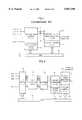
- FIG. 2is a block diagram of an interrupt generating circuit in accordance with the embodiments of the present invention.
- FIG. 3is a detailed circuit diagram of the first comparing circuit in FIG. 2;
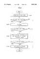
- FIG. 4is a flowchart for explaining an operation of generating an interrupt in accordance with the embodiments of the present invention.
- FIG. 2is a block diagram of an interrupt generating circuit of the present invention
- FIG. 3is a detailed circuit diagram of the first comparing circuit in FIG. 2
- FIG. 4is a flowchart for explaining an operation of generating an interrupt in accordance with the present invention.
- the interrupt generating device of the present inventionincludes a first storing circuit 6, a first comparing circuit 7, an encoding circuit 8, a second comparing circuit 9, a second storing circuit 10, an interrupt request generating circuit 11, and an interrupt enabling circuit 12.
- the first storing circuit 6stores the input/output states of data which are input/output through a plurality of input/output ports A-N.
- the first comparing circuit 7compares the signals A-N received from the first storing circuit 6 with a reference signal and determines whether the signals are in a high-state or a low-state. Based on the determination, the first comparing circuit 7 outputs signals O 1 -O N to the encoding circuit 8.
- the encoding circuit 8encodes the signals O 1 -O N according to the number of signals O 1 -O N being in a high or low state, and outputs encoded signals X 1 -X i to the second comparing circuit 9.
- the second storing circuit 10stores data transmitted from the MCU through a bus 13, and the second comparing circuit 9 compares the data stored in the second storing circuit 10 with the encoded signals X 1 -X i from the encoding circuit 8. The result of the comparison is applied to the interrupt request generating circuit 11.
- the interrupt request generating circuit 11generates an interrupt requesting signal to the MCU through the MCU bus 13.
- the MCUdetermines whether to permit the interrupt and controls the interrupt enabling circuit 12 to enable interrupt, if the interrupt is permitted.
- the first comparing circuit 7includes a PMOS transistor having a power voltage Vcc applied to a drain terminal and a grounded gate terminal, a plurality of NMOS transistors connected to one another in parallel, and a plurality of inverters C 1 -C N connected to the PMOS and NMOS transistors.
- Each of the NMOS transistorshas a gate terminal for receiving one of the signals A-N and a drain terminal connected to a source terminal of the PMOS transistor.
- the plurality of inverters C 1 -C Nare connected to each other in parallel and each of them has an input terminal connected to the drain terminals of the NMOS transistors.
- the first storing circuit 6includes a portion for determining input/output of input/output ports A-N, and a portion for storing the data input or output through the ports A-N.
- the first storing circuit 6stores signals input or output through the plurality of the ports A-N (S101 in FIG. 4). These signals A-N are applied to the first comparing circuit 7.
- the first comparing circuit 7receives the data from the first storing circuit 6, and compares them with a reference signal to detect any high states of the signals (S102).
- the NMOS transistorsreceives the signals A-N applied from the first storing circuit 6, with the gate of the PMOS transistor being grounded.
- each of the NMOS transistors in the first comparing circuit 7has the same size to provide a compact device.
- N-levels of voltageswill appear at node 14 in FIG. 3 depending on the N value of the signal.
- the NMOS transistorsproduce voltages different from one another. These voltages are applied to the inverters C 1 -C N , each inverter having a logic threshold voltage different from one another.
- the inverters C 1 -C Nhave N number of different logic threshold voltages. Therefore, at the node 14, the N-number of voltages different from one another are present from the N number of NMOS transistors, which results in signals O 1 -O N being output by the inverters C 1 -C N .
- the encoding circuit 8receives and encodes the signals O 1 -O N from the inverters C 1 -C N according to a number of high level signals detected, and outputs encoded signals X 1 -X i (S103).
- the encoded signals X 1 -X i from the encoding circuit 8are applied to the second comparing circuit 9.
- the second comparing circuit 9compares the encoded signals received from the encoding circuit 8 with the data in the second storing circuit 10 received through the bus 13, and applies the comparison values to the interrupt request generating circuit 11 (S104).
- the interrupt request generating circuit 11Upon the receipt of the comparison values from the second comparing circuit 9, the interrupt request generating circuit 11 generates an interrupt requesting signal (S105) and applies it to the through the MCU bus 13. In response, the MCU determines whether to permit the interrupt according to its interrupt priority or ignore the interrupt request (S106).
- the MCUapplies to the interrupt request generating circuit 11 an interrupt response by the interrupt enabling circuit 12 outputting an enabling signal.
- the interrupt request generating circuit 11generates an interrupt (S107) and activates the actual interrupt process.
- the request for the interrupt generated by the generating circuit 11is either given a permission or ignored depending on a set or reset signal from the bus 13, i.e., depending on an enable state.
- the interrupt response time period of the MCUis a time period from the time of the interrupt generation to the starting time of an interrupt subroutine. It is known that a shorter response period is desirable.
- the interrupt generating device and method of the present inventiongenerates an interrupt depending on the number of high level voltages received at the input/output ports, and thus prevents the MCU from malfunctioning due to an excessive current flow arising from the activation of many input/output ports.
Landscapes
- Engineering & Computer Science (AREA)
- Theoretical Computer Science (AREA)
- Physics & Mathematics (AREA)
- General Engineering & Computer Science (AREA)
- General Physics & Mathematics (AREA)
- Bus Control (AREA)
- Microcomputers (AREA)
Abstract
Description
Claims (17)
Applications Claiming Priority (2)
| Application Number | Priority Date | Filing Date | Title |
|---|---|---|---|
| KR1019950042552AKR0156173B1 (en) | 1995-11-21 | 1995-11-21 | Interrupt Generation Circuit |
| KR199542552 | 1995-11-21 |
Publications (1)
| Publication Number | Publication Date |
|---|---|
| US5857108Atrue US5857108A (en) | 1999-01-05 |
Family
ID=19434962
Family Applications (1)
| Application Number | Title | Priority Date | Filing Date |
|---|---|---|---|
| US08/649,099Expired - Fee RelatedUS5857108A (en) | 1995-11-21 | 1996-05-17 | Device and method for generating interrupts |
Country Status (4)
| Country | Link |
|---|---|
| US (1) | US5857108A (en) |
| JP (1) | JP2826998B2 (en) |
| KR (1) | KR0156173B1 (en) |
| DE (1) | DE19648078A1 (en) |
Cited By (14)
| Publication number | Priority date | Publication date | Assignee | Title |
|---|---|---|---|---|
| US5931936A (en)* | 1996-12-04 | 1999-08-03 | Electronics And Telecommunications Research Institute | Multiple interrupt controller and control method using an intelligent priority-decision mechanism |
| US6035361A (en)* | 1997-11-28 | 2000-03-07 | Electronics And Telecommunications Research Institute | Cell bus arbitration device and method arbitrating the same |
| US6223246B1 (en)* | 1997-12-24 | 2001-04-24 | Kabushiki Kaisha Toshiba | Computer system having an interrupt handler |
| US6510480B1 (en)* | 1998-08-25 | 2003-01-21 | Matsushita Electric Industrial Co., Ltd. | Data transfer circuit and data processing method using data transfer circuit for handling interruption processing |
| EP1134665A3 (en)* | 2000-03-17 | 2004-01-14 | Exar Corporation | UART with compressed user accessible interrupt codes |
| US20050054384A1 (en)* | 2003-08-22 | 2005-03-10 | Sbc Knowledge Ventures, L.P. | System and method for prioritized interface design |
| US20050273540A1 (en)* | 2004-05-11 | 2005-12-08 | Stmicroelectronics Limited | Interrupt handling system |
| US20060010206A1 (en)* | 2003-10-15 | 2006-01-12 | Microsoft Corporation | Guiding sensing and preferences for context-sensitive services |
| US20070005860A1 (en)* | 2005-06-29 | 2007-01-04 | Inventec Corporation | Interrupt control system and method |
| US20070255876A1 (en)* | 2006-04-28 | 2007-11-01 | Nec Electronics Corporation | Interrupt control circuit and method |
| US20090204739A1 (en)* | 2008-02-12 | 2009-08-13 | Broadcom Corporation | Interruptible write block and method for using same |
| US20120277642A1 (en)* | 2011-04-28 | 2012-11-01 | Zoll Circulation, Inc. | System and method for automated detection of battery insert |
| TWI695268B (en)* | 2015-08-03 | 2020-06-01 | 巴貝多商馬維爾國際貿易有限公司 | Systems and methods for transmitting interrupts between nodes |
| US11177667B2 (en) | 2011-04-28 | 2021-11-16 | Zoll Circulation, Inc. | Viral distribution of battery management parameters |
Families Citing this family (1)
| Publication number | Priority date | Publication date | Assignee | Title |
|---|---|---|---|---|
| KR100517499B1 (en)* | 2002-10-18 | 2005-09-28 | 삼성전자주식회사 | Method and apparatus for detecting connection condition between transmitter and receiver |
Citations (17)
| Publication number | Priority date | Publication date | Assignee | Title |
|---|---|---|---|---|
| US4961067A (en)* | 1986-07-28 | 1990-10-02 | Motorola, Inc. | Pattern driven interrupt in a digital data processor |
| US5101497A (en)* | 1988-09-09 | 1992-03-31 | Compaq Computer Corporation | Programmable interrupt controller |
| US5133056A (en)* | 1988-09-05 | 1992-07-21 | Kabushiki Kaisha Toshiba | Interrupt controller |
| US5179704A (en)* | 1991-03-13 | 1993-01-12 | Ncr Corporation | Method and apparatus for generating disk array interrupt signals |
| US5193195A (en)* | 1989-09-22 | 1993-03-09 | Nec Corporation | Microcomputer having easily testable interrupt controller |
| US5410715A (en)* | 1990-02-20 | 1995-04-25 | Nec Corporation | Interrupt controller with selectable interrupt nesting function |
| US5471620A (en)* | 1993-06-29 | 1995-11-28 | Mitsubishi Denki Kabushiki Kaisha | Data processor with means for separately receiving and processing different types of interrupts |
| US5530903A (en)* | 1992-06-30 | 1996-06-25 | International Business Machines Corporation | System for reassigning a higher priority to an interrupted user by inhibiting the access of other users until the interrupted user has completed its task |
| US5555413A (en)* | 1995-02-17 | 1996-09-10 | International Business Machines Corporation | Computer system and method with integrated level and edge interrupt requests at the same interrupt priority |
| US5560019A (en)* | 1991-09-27 | 1996-09-24 | Sun Microsystems, Inc. | Method and apparatus for handling interrupts in a multiprocessor computer system |
| US5572151A (en)* | 1994-08-08 | 1996-11-05 | Hitachi, Ltd. | Pass transistor type selector circuit and digital logic circuit |
| US5581771A (en)* | 1993-10-08 | 1996-12-03 | Nec Corporation | Microcomputer having interrupt control circuit to determine priority level |
| US5584028A (en)* | 1990-05-14 | 1996-12-10 | At&T Global Information Solutions Company | Method and device for processing multiple, asynchronous interrupt signals |
| US5615375A (en)* | 1992-11-17 | 1997-03-25 | Fujitsu Limited | Interrupt control circuit |
| US5617429A (en)* | 1993-08-30 | 1997-04-01 | Mitsubishi Denki Kabushiki Kaisha | Failure detection system for detecting failure of functional blocks of integrated circuits |
| US5640571A (en)* | 1995-03-01 | 1997-06-17 | Intel Corporation | Interrupt steering for a computer system |
| US5659760A (en)* | 1992-02-18 | 1997-08-19 | Nec Corporation | Microprocessor having interrupt vector generation unit and vector fetching command unit to initiate interrupt processing prior to returning interrupt acknowledge information |
Family Cites Families (6)
| Publication number | Priority date | Publication date | Assignee | Title |
|---|---|---|---|---|
| JPS6118059A (en)* | 1984-07-05 | 1986-01-25 | Nec Corp | Memory circuit |
| JPH025141A (en)* | 1988-06-24 | 1990-01-10 | Nec Corp | Microcomputer |
| JPH0237422A (en)* | 1988-07-28 | 1990-02-07 | Oki Electric Ind Co Ltd | Numerical management system |
| US5187781A (en)* | 1989-12-19 | 1993-02-16 | International Business Machines Corp. | Shared hardware interrupt circuit for personal computers |
| JPH05134807A (en)* | 1991-11-11 | 1993-06-01 | Matsushita Electron Corp | A/d converter |
| US5455774A (en)* | 1992-10-22 | 1995-10-03 | Motorola, Inc. | Interrupt programmable analog-to-digital port |
- 1995
- 1995-11-21KRKR1019950042552Apatent/KR0156173B1/ennot_activeExpired - Fee Related
- 1996
- 1996-05-17USUS08/649,099patent/US5857108A/ennot_activeExpired - Fee Related
- 1996-11-11JPJP8312621Apatent/JP2826998B2/ennot_activeExpired - Fee Related
- 1996-11-20DEDE19648078Apatent/DE19648078A1/ennot_activeCeased
Patent Citations (17)
| Publication number | Priority date | Publication date | Assignee | Title |
|---|---|---|---|---|
| US4961067A (en)* | 1986-07-28 | 1990-10-02 | Motorola, Inc. | Pattern driven interrupt in a digital data processor |
| US5133056A (en)* | 1988-09-05 | 1992-07-21 | Kabushiki Kaisha Toshiba | Interrupt controller |
| US5101497A (en)* | 1988-09-09 | 1992-03-31 | Compaq Computer Corporation | Programmable interrupt controller |
| US5193195A (en)* | 1989-09-22 | 1993-03-09 | Nec Corporation | Microcomputer having easily testable interrupt controller |
| US5410715A (en)* | 1990-02-20 | 1995-04-25 | Nec Corporation | Interrupt controller with selectable interrupt nesting function |
| US5584028A (en)* | 1990-05-14 | 1996-12-10 | At&T Global Information Solutions Company | Method and device for processing multiple, asynchronous interrupt signals |
| US5179704A (en)* | 1991-03-13 | 1993-01-12 | Ncr Corporation | Method and apparatus for generating disk array interrupt signals |
| US5560019A (en)* | 1991-09-27 | 1996-09-24 | Sun Microsystems, Inc. | Method and apparatus for handling interrupts in a multiprocessor computer system |
| US5659760A (en)* | 1992-02-18 | 1997-08-19 | Nec Corporation | Microprocessor having interrupt vector generation unit and vector fetching command unit to initiate interrupt processing prior to returning interrupt acknowledge information |
| US5530903A (en)* | 1992-06-30 | 1996-06-25 | International Business Machines Corporation | System for reassigning a higher priority to an interrupted user by inhibiting the access of other users until the interrupted user has completed its task |
| US5615375A (en)* | 1992-11-17 | 1997-03-25 | Fujitsu Limited | Interrupt control circuit |
| US5471620A (en)* | 1993-06-29 | 1995-11-28 | Mitsubishi Denki Kabushiki Kaisha | Data processor with means for separately receiving and processing different types of interrupts |
| US5617429A (en)* | 1993-08-30 | 1997-04-01 | Mitsubishi Denki Kabushiki Kaisha | Failure detection system for detecting failure of functional blocks of integrated circuits |
| US5581771A (en)* | 1993-10-08 | 1996-12-03 | Nec Corporation | Microcomputer having interrupt control circuit to determine priority level |
| US5572151A (en)* | 1994-08-08 | 1996-11-05 | Hitachi, Ltd. | Pass transistor type selector circuit and digital logic circuit |
| US5555413A (en)* | 1995-02-17 | 1996-09-10 | International Business Machines Corporation | Computer system and method with integrated level and edge interrupt requests at the same interrupt priority |
| US5640571A (en)* | 1995-03-01 | 1997-06-17 | Intel Corporation | Interrupt steering for a computer system |
Cited By (20)
| Publication number | Priority date | Publication date | Assignee | Title |
|---|---|---|---|---|
| US5931936A (en)* | 1996-12-04 | 1999-08-03 | Electronics And Telecommunications Research Institute | Multiple interrupt controller and control method using an intelligent priority-decision mechanism |
| US6035361A (en)* | 1997-11-28 | 2000-03-07 | Electronics And Telecommunications Research Institute | Cell bus arbitration device and method arbitrating the same |
| US6223246B1 (en)* | 1997-12-24 | 2001-04-24 | Kabushiki Kaisha Toshiba | Computer system having an interrupt handler |
| US6510480B1 (en)* | 1998-08-25 | 2003-01-21 | Matsushita Electric Industrial Co., Ltd. | Data transfer circuit and data processing method using data transfer circuit for handling interruption processing |
| EP1134665A3 (en)* | 2000-03-17 | 2004-01-14 | Exar Corporation | UART with compressed user accessible interrupt codes |
| US6947999B1 (en) | 2000-03-17 | 2005-09-20 | Exar Corporation | UART with compressed user accessible interrupt codes |
| US20050054384A1 (en)* | 2003-08-22 | 2005-03-10 | Sbc Knowledge Ventures, L.P. | System and method for prioritized interface design |
| US7831679B2 (en)* | 2003-10-15 | 2010-11-09 | Microsoft Corporation | Guiding sensing and preferences for context-sensitive services |
| US20060010206A1 (en)* | 2003-10-15 | 2006-01-12 | Microsoft Corporation | Guiding sensing and preferences for context-sensitive services |
| US20050273540A1 (en)* | 2004-05-11 | 2005-12-08 | Stmicroelectronics Limited | Interrupt handling system |
| US20070005860A1 (en)* | 2005-06-29 | 2007-01-04 | Inventec Corporation | Interrupt control system and method |
| US20070255876A1 (en)* | 2006-04-28 | 2007-11-01 | Nec Electronics Corporation | Interrupt control circuit and method |
| US7707343B2 (en)* | 2006-04-28 | 2010-04-27 | Nec Electronics Corporation | Interrupt control circuit and method |
| US20090204739A1 (en)* | 2008-02-12 | 2009-08-13 | Broadcom Corporation | Interruptible write block and method for using same |
| US8433857B2 (en)* | 2008-02-12 | 2013-04-30 | Broadcom Corporation | Interruptible write block and method for using same |
| US20120277642A1 (en)* | 2011-04-28 | 2012-11-01 | Zoll Circulation, Inc. | System and method for automated detection of battery insert |
| US9825475B2 (en)* | 2011-04-28 | 2017-11-21 | Zoll Circulation, Inc. | System and method for automated detection of battery insert |
| US11177667B2 (en) | 2011-04-28 | 2021-11-16 | Zoll Circulation, Inc. | Viral distribution of battery management parameters |
| US12107444B2 (en) | 2011-04-28 | 2024-10-01 | Zoll Circulation, Inc. | Viral distribution of battery management parameters |
| TWI695268B (en)* | 2015-08-03 | 2020-06-01 | 巴貝多商馬維爾國際貿易有限公司 | Systems and methods for transmitting interrupts between nodes |
Also Published As
| Publication number | Publication date |
|---|---|
| JP2826998B2 (en) | 1998-11-18 |
| KR970029097A (en) | 1997-06-26 |
| DE19648078A1 (en) | 1997-05-22 |
| KR0156173B1 (en) | 1998-11-16 |
| JPH09160785A (en) | 1997-06-20 |
Similar Documents
| Publication | Publication Date | Title |
|---|---|---|
| US5857108A (en) | Device and method for generating interrupts | |
| JP4115494B2 (en) | Automatic voltage detection when multiple voltages are applied | |
| US5473635A (en) | Data communication circuit | |
| US5613130A (en) | Card voltage switching and protection | |
| KR20190099933A (en) | Memory Device determining operation mode based on external voltage and Operating Method thereof | |
| US4543494A (en) | MOS type output driver circuit having a protective circuit | |
| US6327635B1 (en) | Add-on card with automatic bus power line selection circuit | |
| US6529422B1 (en) | Input stage apparatus and method having a variable reference voltage | |
| US5477172A (en) | Configurable input buffer dependent on supply voltage | |
| KR102799338B1 (en) | Calibration control circuit and stroage device comprising the calibration control circuit | |
| US4419592A (en) | Bidirection data switch sequencing circuit | |
| US6857040B2 (en) | Bi-directional bus bridge in which multiple devices can assert bus concurrently | |
| US5642480A (en) | Method and apparatus for enhanced security of a data processor | |
| US7073078B2 (en) | Power control unit that provides one of a plurality of voltages on a common power rail | |
| US5737571A (en) | System for discriminating that an external processor is permitted to access a data storage device utilizing prescribed control signals including access enable signal | |
| US20050185449A1 (en) | Nonvolatile data storage apparatus | |
| KR100424451B1 (en) | Method and apparatus for fast production programming and low-voltage in-system writes for programmable logic device | |
| US5265256A (en) | Data processing system having a programmable mode for selecting operation at one of a plurality of power supply potentials | |
| US7080185B2 (en) | Bus control device altering drive capability according to condition | |
| US5870623A (en) | I/O port for determining accidents in an external device | |
| KR0169604B1 (en) | Data output buffer selecting apparatus in semiconductor | |
| KR100345878B1 (en) | Improved output circuit for a low voltage eprom | |
| KR0167261B1 (en) | The control circuit for power supply | |
| EP1243111A1 (en) | Method and circuit for protection of a universal serial bus transceiver against short-circuit | |
| US6784691B2 (en) | Integrated circuit having a connection pad for stipulating one of a plurality of organization forms, and method for operating the circuit |
Legal Events
| Date | Code | Title | Description |
|---|---|---|---|
| AS | Assignment | Owner name:LG SEMICON CO., LTD., KOREA, REPUBLIC OF Free format text:ASSIGNMENT OF ASSIGNORS INTEREST;ASSIGNOR:HONG, SANG PYO;REEL/FRAME:008221/0425 Effective date:19960921 | |
| FEPP | Fee payment procedure | Free format text:PAYOR NUMBER ASSIGNED (ORIGINAL EVENT CODE: ASPN); ENTITY STATUS OF PATENT OWNER: LARGE ENTITY | |
| FPAY | Fee payment | Year of fee payment:4 | |
| AS | Assignment | Owner name:HYNIX SEMICONDUCTOR INC., KOREA, REPUBLIC OF Free format text:CHANGE OF NAME;ASSIGNOR:LG SEMICON CO., LTD.;REEL/FRAME:015246/0634 Effective date:19990726 | |
| AS | Assignment | Owner name:MAGNACHIP SEMICONDUCTOR, LTD., KOREA, REPUBLIC OF Free format text:ASSIGNMENT OF ASSIGNORS INTEREST;ASSIGNOR:HYNIX SEMICONDUCTOR, INC.;REEL/FRAME:016216/0649 Effective date:20041004 | |
| AS | Assignment | Owner name:U.S. BANK NATIONAL ASSOCIATION, AS COLLATERAL TRUS Free format text:SECURITY INTEREST;ASSIGNOR:MAGNACHIP SEMICONDUCTOR, LTD.;REEL/FRAME:016470/0530 Effective date:20041223 | |
| REMI | Maintenance fee reminder mailed | ||
| LAPS | Lapse for failure to pay maintenance fees | ||
| STCH | Information on status: patent discontinuation | Free format text:PATENT EXPIRED DUE TO NONPAYMENT OF MAINTENANCE FEES UNDER 37 CFR 1.362 | |
| FP | Lapsed due to failure to pay maintenance fee | Effective date:20070105 |