US5855687A - Substrate support shield in wafer processing reactors - Google Patents
Substrate support shield in wafer processing reactorsDownload PDFInfo
- Publication number
- US5855687A US5855687AUS08/326,506US32650694AUS5855687AUS 5855687 AUS5855687 AUS 5855687AUS 32650694 AUS32650694 AUS 32650694AUS 5855687 AUS5855687 AUS 5855687A
- Authority
- US
- United States
- Prior art keywords
- susceptor
- wafer
- chamber
- substrate
- recited
- Prior art date
- Legal status (The legal status is an assumption and is not a legal conclusion. Google has not performed a legal analysis and makes no representation as to the accuracy of the status listed.)
- Expired - Lifetime
Links
Images


Classifications
- C—CHEMISTRY; METALLURGY
- C23—COATING METALLIC MATERIAL; COATING MATERIAL WITH METALLIC MATERIAL; CHEMICAL SURFACE TREATMENT; DIFFUSION TREATMENT OF METALLIC MATERIAL; COATING BY VACUUM EVAPORATION, BY SPUTTERING, BY ION IMPLANTATION OR BY CHEMICAL VAPOUR DEPOSITION, IN GENERAL; INHIBITING CORROSION OF METALLIC MATERIAL OR INCRUSTATION IN GENERAL
- C23C—COATING METALLIC MATERIAL; COATING MATERIAL WITH METALLIC MATERIAL; SURFACE TREATMENT OF METALLIC MATERIAL BY DIFFUSION INTO THE SURFACE, BY CHEMICAL CONVERSION OR SUBSTITUTION; COATING BY VACUUM EVAPORATION, BY SPUTTERING, BY ION IMPLANTATION OR BY CHEMICAL VAPOUR DEPOSITION, IN GENERAL
- C23C16/00—Chemical coating by decomposition of gaseous compounds, without leaving reaction products of surface material in the coating, i.e. chemical vapour deposition [CVD] processes
- C23C16/44—Chemical coating by decomposition of gaseous compounds, without leaving reaction products of surface material in the coating, i.e. chemical vapour deposition [CVD] processes characterised by the method of coating
- C23C16/455—Chemical coating by decomposition of gaseous compounds, without leaving reaction products of surface material in the coating, i.e. chemical vapour deposition [CVD] processes characterised by the method of coating characterised by the method used for introducing gases into reaction chamber or for modifying gas flows in reaction chamber
- C23C16/45519—Inert gas curtains
- C23C16/45521—Inert gas curtains the gas, other than thermal contact gas, being introduced the rear of the substrate to flow around its periphery
- C—CHEMISTRY; METALLURGY
- C23—COATING METALLIC MATERIAL; COATING MATERIAL WITH METALLIC MATERIAL; CHEMICAL SURFACE TREATMENT; DIFFUSION TREATMENT OF METALLIC MATERIAL; COATING BY VACUUM EVAPORATION, BY SPUTTERING, BY ION IMPLANTATION OR BY CHEMICAL VAPOUR DEPOSITION, IN GENERAL; INHIBITING CORROSION OF METALLIC MATERIAL OR INCRUSTATION IN GENERAL
- C23C—COATING METALLIC MATERIAL; COATING MATERIAL WITH METALLIC MATERIAL; SURFACE TREATMENT OF METALLIC MATERIAL BY DIFFUSION INTO THE SURFACE, BY CHEMICAL CONVERSION OR SUBSTITUTION; COATING BY VACUUM EVAPORATION, BY SPUTTERING, BY ION IMPLANTATION OR BY CHEMICAL VAPOUR DEPOSITION, IN GENERAL
- C23C16/00—Chemical coating by decomposition of gaseous compounds, without leaving reaction products of surface material in the coating, i.e. chemical vapour deposition [CVD] processes
- C23C16/04—Coating on selected surface areas, e.g. using masks
- C23C16/042—Coating on selected surface areas, e.g. using masks using masks
- C—CHEMISTRY; METALLURGY
- C23—COATING METALLIC MATERIAL; COATING MATERIAL WITH METALLIC MATERIAL; CHEMICAL SURFACE TREATMENT; DIFFUSION TREATMENT OF METALLIC MATERIAL; COATING BY VACUUM EVAPORATION, BY SPUTTERING, BY ION IMPLANTATION OR BY CHEMICAL VAPOUR DEPOSITION, IN GENERAL; INHIBITING CORROSION OF METALLIC MATERIAL OR INCRUSTATION IN GENERAL
- C23C—COATING METALLIC MATERIAL; COATING MATERIAL WITH METALLIC MATERIAL; SURFACE TREATMENT OF METALLIC MATERIAL BY DIFFUSION INTO THE SURFACE, BY CHEMICAL CONVERSION OR SUBSTITUTION; COATING BY VACUUM EVAPORATION, BY SPUTTERING, BY ION IMPLANTATION OR BY CHEMICAL VAPOUR DEPOSITION, IN GENERAL
- C23C16/00—Chemical coating by decomposition of gaseous compounds, without leaving reaction products of surface material in the coating, i.e. chemical vapour deposition [CVD] processes
- C23C16/44—Chemical coating by decomposition of gaseous compounds, without leaving reaction products of surface material in the coating, i.e. chemical vapour deposition [CVD] processes characterised by the method of coating
- C23C16/458—Chemical coating by decomposition of gaseous compounds, without leaving reaction products of surface material in the coating, i.e. chemical vapour deposition [CVD] processes characterised by the method of coating characterised by the method used for supporting substrates in the reaction chamber
- C23C16/4582—Rigid and flat substrates, e.g. plates or discs
- C23C16/4583—Rigid and flat substrates, e.g. plates or discs the substrate being supported substantially horizontally
- C23C16/4585—Devices at or outside the perimeter of the substrate support, e.g. clamping rings, shrouds
- H—ELECTRICITY
- H01—ELECTRIC ELEMENTS
- H01L—SEMICONDUCTOR DEVICES NOT COVERED BY CLASS H10
- H01L21/00—Processes or apparatus adapted for the manufacture or treatment of semiconductor or solid state devices or of parts thereof
- H01L21/67—Apparatus specially adapted for handling semiconductor or electric solid state devices during manufacture or treatment thereof; Apparatus specially adapted for handling wafers during manufacture or treatment of semiconductor or electric solid state devices or components ; Apparatus not specifically provided for elsewhere
- H01L21/683—Apparatus specially adapted for handling semiconductor or electric solid state devices during manufacture or treatment thereof; Apparatus specially adapted for handling wafers during manufacture or treatment of semiconductor or electric solid state devices or components ; Apparatus not specifically provided for elsewhere for supporting or gripping
- H01L21/687—Apparatus specially adapted for handling semiconductor or electric solid state devices during manufacture or treatment thereof; Apparatus specially adapted for handling wafers during manufacture or treatment of semiconductor or electric solid state devices or components ; Apparatus not specifically provided for elsewhere for supporting or gripping using mechanical means, e.g. chucks, clamps or pinches
- H01L21/68714—Apparatus specially adapted for handling semiconductor or electric solid state devices during manufacture or treatment thereof; Apparatus specially adapted for handling wafers during manufacture or treatment of semiconductor or electric solid state devices or components ; Apparatus not specifically provided for elsewhere for supporting or gripping using mechanical means, e.g. chucks, clamps or pinches the wafers being placed on a susceptor, stage or support
- H01L21/68735—Apparatus specially adapted for handling semiconductor or electric solid state devices during manufacture or treatment thereof; Apparatus specially adapted for handling wafers during manufacture or treatment of semiconductor or electric solid state devices or components ; Apparatus not specifically provided for elsewhere for supporting or gripping using mechanical means, e.g. chucks, clamps or pinches the wafers being placed on a susceptor, stage or support characterised by edge profile or support profile
Definitions
- This inventionrelates to apparatus for chemical vapor deposition (CVD) on semiconductor wafers and, more specifically, to a shield for shielding the upper edge of a susceptor to prevent deposition thereon.
- CVDchemical vapor deposition
- CVDchemical vapor deposition
- FIG. 1a typical reactor used for CVD processing of a semiconductor wafer is illustrated in FIG. 1.
- a wafer 10is supported on a circular susceptor 11 beneath a gas inlet or shower head 12.
- Processing/deposition gas containing molecules comprising a metallic cation, such as Tungstenenters the CVD chamber through the shower head 12 and reacts adjacent to the wafer so that the metal is deposited on the face or top surface of the wafer 10.
- a shadow ring 13overhangs and is supported by the edge of the wafer 10.
- the shadow ring 13defines an exclusionary zone, typically 1.5 to 2.0 mm wide around the perimeter of the wafer, onto which no deposition occurs.
- the purpose of creating this zoneis to exclude deposited materials from this zone, the edge and the backside of the wafer and thereby reduce the generation of unwanted particles in the chamber. This is a particularly important where the deposited material does not adhere to such areas.
- Tungstendoes not readily adhere to certain surfaces and before it is deposited over silicon oxide on a semiconductor wafer, the oxide surfaces must be pretreated for the tungsten being deposited to properly adhere to the surfaces (e.g. by deposition of a Titanium Tungsten (TiW)) or Titanium Nitride (TiN)). Typically, the edge and backside of the wafer surfaces have not been pretreated and any deposited Tungsten would not adhere properly and tend to flake off in particles.
- TiWTitanium Tungsten
- TiNTitanium Nitride
- the exclusionary zonealso provides a "buffer" zone which, when contacted by wafer handling equipment, does not readily chip or flake as would a fully/or inadequately processed surface. Such chipping and flaking could also result in unwanted particle generation.
- a pumping ring 14is located on a supporting lip or shoulder 15 inside the chamber and has an inner diameter such that an annular gap is defined between the ring 14 and the outer edge of the susceptor 11.
- a non-reactive purge gasis introduced, at a pressure greater than the pressure of the deposition gas, into the chamber from a position below the susceptor. This purging gas flows from below the susceptor 11 to the region above it through the annular gap.
- the purpose of the purging gas flowis to inhibit passage of the deposition gas into the region below the susceptor and, thereby, help prevent unwanted deposition on the surfaces of the elements of the reactor that are located in this region.
- the shadow ring 13rests on both the susceptor 11 and the pumping ring 14. As such, it partially obstructs the annular gap, defined between the susceptor and the pumping ring, and thereby further controls the flow of purging gas from below to beneath the susceptor.
- the problem with the apparatus illustrated in this figureis that it cannot be used in applications where deposition is to occur over the entire surface of the wafer. This is so even if the shadow ring were removed, because of how a wafer is heated in processing reactors.
- Depositionis effected by, amongst others, the temperature of the wafer.
- the susceptoris heated by means of, for example, heater lamps. The heated susceptor then conductively heats the wafer.
- any heated susceptorIn any heated susceptor a certain amount of heat loss will occur at the edges resulting in a temperature drop off toward the edges of the susceptor, with its perimeter regions being cooler than its central region.
- susceptor described abovewhich is approximately the same diameter as the wafer, heats the wafer less at the edges than at the center. This, in turn, leads to non-uniform and less easily controlled deposition over the entire wafer.
- the susceptordoes not solve the problem.
- An enlarged susceptorwould have surface areas that are exposed to deposition.
- Such depositionmust be removed, before the next process cycle commences, by means of a cleaning process that usually is achieved by plasma etching.
- plasma etchingis very effective on the quartz and alumina components or surfaces in the chamber, the susceptor is made of anodized aluminum. This material is not as resistive to the plasma etch and would rapidly wear away. Accordingly, any deposition on the susceptor which would need to be removed by plasma etching would be very disadvantageous.
- the apparatusshould preferably also minimize edge and backside deposition on the wafer, for the reasons set out above.
- a single substrate CVD wafer processing reactorincludes a chamber housing a wafer supporting susceptor and a shower head for introducing processing gas into the chamber towards the top face of the wafer.
- the susceptorhas an outer diameter that is greater than the outer diameter of the wafer.
- a shield ringrests on and covers a substantial portion of the susceptor which protrudes beyond the outer perimeter of the wafer. This prevents disadvantageous deposition on the susceptor.
- the waferis typically supported within a pocket in the upper face of the susceptor.
- a grooveis formed in the floor of the pocket at its perimeter and acts both as a "thermal choke” to improve the uniformity of temperature within the portion of the susceptor directly below the wafer and as a receptacle for deposition build-up at the edge of the wafer.
- the shield ringmay include a plurality of centering protrusions, at least some of which engage the susceptor as it moves upwards to lift the shield ring off its supports in the chamber.
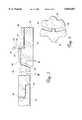
- FIG. 1is a schematic cross section illustrating a prior art reactor
- FIG. 2is a similar cross section illustrating the reactor of the invention
- FIG. 3is a cross sectional detail of the interface between the shield ring and the susceptor further illustrating the invention.
- FIG. 4is sectional detail of the shield ring taken along line 4--4 in FIG. 3.
- FIG. 2is a schematic cross section through a typical single wafer, CVD, semiconductor wafer processing reactor.
- the reactor 20includes a housing 22 that defines a processing chamber 24 inside which a susceptor 26 is located.
- the susceptor 26divides the chamber into upper and lower portions 24a and 24b, respectively.
- the susceptorsupports on its upper surface a semiconductor wafer 28 beneath a shower head 30 having a planar array of closely spaced apertures through which gas containing metal atoms can be injected into the chamber 24 for deposition on the wafer 28.
- the susceptor 26is moveable vertically along and is rotatable about a central axis 31 that is perpendicular to the primary plane of the wafer 28, under action of a lift mechanism 32.
- the susceptor and the chamber interiorare heated by radiant energy sources such as heater lamps 34 located below the housing 22 or alternatively by a resistive heater in the susceptor 26.
- the lower wall 36 of the housing 22is of a material, such as quartz, which is transparent to radiant energy from the heater lamps 34.
- the heated susceptor 26,heats the wafer 28, at least partially through conduction.
- the susceptorhas a larger diameter than the wafer.
- the susceptorwill have a diameter of 6.394 inches (163 mm) leaving a projecting portion beyond the outer perimeter of the wafer.
- a shield ring 40is positioned around the outer perimeter of the susceptor 26.
- the pumping plate 42is secured to the outer wall of the chamber 24 in a conventional manner at a point approximately 1" (25.4 mm) below the shower head 30.
- the shield ring 40is lifted off the pumping plate 42 by the susceptor 26 and is supported by the peripheral projecting portion of the susceptor 26.
- This figurealso illustrates that the housing 22 includes a purge gas inlet 38 through which purge gas is injected into the lower portion 24b of the chamber.
- FIG. 3is an enlarged cross section of these components. It should be noted here the specific dimensions given below with respect to this figure are illustrative in nature and should accordingly not be seen as limiting the concept of this invention.
- the susceptor 26includes a recessed pocket 43 formed therein.
- This pocketis sized to receive the wafer 28 and is dimensioned to have a slightly larger diameter and be slightly deeper than the wafer's diameter and thickness, respectively. So, for example, for a wafer that is 150 mm in diameter, the pocket may have an interior diameter of 5.995" to 6.0" (152.27 to 152.40 mm). Typically, such 150 mm wafer is 0.028" to 0.034" inches (0.711 to 0.864 mm) thick. In this case the corresponding pocket would be 0.035" to 0.040" (0.889 to 1.016 mm) deep.
- a groove 44 of semi-circular cross-sectionis cut into its floor.
- This grooveis peripherally approximately 0.035" to 0.040" (0.889 to 1.016 mm) wide at the top and formed with a radius of approximately 0.018 to 0.020" (0.457 to 0.508 mm).
- the groove 44the wafer edge bevel 45.
- the groove 44has two functions. Firstly, it functions as a thermal "choke” as it reduces the cross section of the susceptor 26 at the perimeter of the wafer. It is known that thermal conduction within a body of material, such as the susceptor 26, is related to the cross section of the material making up the body. As the cross sectional area of the material decreases so too does its ability to transfer thermal energy (heat) across such zone of decreased cross sectional area. As described above, the susceptor 26 heats the wafer 28 by conduction, at least within the susceptor itself. In CVD applications it is generally preferable for the wafer 28 to be uniformly heated across its entire surface. To best achieve this, the portion of the susceptor 26 located directly below the wafer 28 should have a uniform temperature.
- the groove 44in reducing the cross sectional area of the susceptor at the perimeter of the wafer, and thereby acting as a thermal choke, assists in this. If it were not for the thermal choke effect of the groove 44, the temperature of the susceptor 26, which would otherwise naturally drop off towards its outer perimeter, would reduce from within the portion of the susceptor 26 beneath the wafer 28.
- the grooveacts to receive deposition which would otherwise build up at the edge of the wafer. This deposition build-up could detrimentally lift the wafer off the susceptor's surface resulting in unwanted backside deposition and possible effecting the heating of the wafer by conduction from the susceptor.
- the shield ring 40is typically 0.2" (5.08 mm) thick across its thickest portion. In applications with 150-mm diameter wafers, the internal diameter of the ring 40 is slightly greater than 150 mm and the maximum external diameter of the ring 40 is approximately 7.808" (195.2 mm).
- the ring 40has a first step 46 formed in its bottom surface. This first step, which is typically 0.064" (1.63 mm) thick and approximately 0.621 “ (15.78 mm) wide, is shaped to interact with a complementarily shaped step formed in the top of pumping plate 42.
- a second stepis formed in the bottom surface to define a roof 48 overhanging the susceptor.
- the overhanging roof portionis approximately 0.62 inches (15.75 mm) wide and 0.035" (0.89 mm) thick at its thickest portion 50, being is the portion of the roof 48 closest to the central axis 31.
- this thickest portion of the roof 48engages the susceptor 26 at a line of contact 52.
- the roof 48tapers at approximately 0° 3.3' away from the susceptor 26 to become thinner in cross section further away from the central axis 31.
- This arrangementensures that the shield ring 40 contacts the susceptor 26 at the line of contact 52 as close to the wafer as possible and, thereby, minimizes deposition on the upper surface of the susceptor 26.
- the interior edge 54 of the roof 48slopes inwardly and upwardly from the line of contact 52 at an angle of approximately 5° from the vertical. This creates a "shadow" on the susceptor 26 which reduces deposition on any exposed portions of the upper surface of the susceptor 26. It also reduces the amount of deposition in the groove 44 formed at the edge of the pocket 43.
- this figureshows that the inner face 56 of the main body of the shield ring 40 is sloped downwardly and outwardly. In practice, this slope is at an angle of approximately 30°.
- This sloping inner face 56is generally parallel with a sloping outer surface of the susceptor 26 and serves to assist centering the susceptor within the shield ring 40 as the susceptor 26 is moved up and down during processing cycles.
- the shield ring 40includes six tabs 60, one of which is illustrated plan cross-section in FIG. 4. These six tabs 60 are equally spaced around the inner face 56 of the shield ring 40 and extend generally vertically upward along the entire inward sloping surface 56 of the shield ring 40. Typically, these tabs are 0.09 inches (2.286 mm) in cross sectional width and protrude 0.10 inches (0.25 mm) toward the center of the wafer from the sloping face 56. It has been found that, as the susceptor 26 moves up to engage the shield ring 40, at least three of these tabs 60 make contact with the sloping outer surface 56 of the susceptor.
- the tabs 60provide point contacts which substantially reduce the "heat sink” effect of the shield ring 40 by substantially reducing the contact area available for conductive transfer of heat between the susceptor 26 and the shield ring 40. This substantially reduced area of contact also reduces the chance of sticking between the shield ring and the susceptor 26.
- these tabs 60serve, as indicated above, to center the shield 40 and the susceptor 26 with respect to each other. These tabs 60 increase the machining tolerances and provide, at a minimum, a stable, three point contact between the susceptor 26 and the shield ring 40.
- the reactor 20 described aboveoperates as follows. To commence processing, the susceptor 26 moves downwardly under action of lift 32 into the lower portion 24b of the chamber 20. A wafer 28 is inserted into the chamber and placed onto the susceptor 26 by conventional robot arm and lift pins (not shown). The susceptor 26 then moves back up to make contact, at line of contact 52, with the shield ring 40. As the susceptor 26 moves upwardly, and as described above, the six tabs 60 located along the inner face 56 of the shield ring ensure that the shield ring is properly centered with respect to the susceptor 26.
- the susceptor 26As the susceptor 26 continues to move upwardly it lifts the shield ring 40 slightly up from the pumping plate 42 to form a serpentine space 58 between the shield ring 40 and the pumping plate 42. At a point when the wafer is approximately 0.250" to 0.500" (6.35 to 12.7 mm) from the shower head 30, the susceptor 26 stops and processing is initiated.
- the interior of chamber and, more particularly, the susceptor 26are heated by means of radiant energy from the heater lamps 34. As the susceptor heats up, it heats the wafer 28 by means of conduction. To ensure uniformity of heating and uniformity of deposition, the susceptor 26 is rotated about the central axis 31. This rotation is achieved by conventional means by a lift mechanism 32 which can further rotate.
- purge gasis introduced into the lower portion 24b of the chamber 20 via the purge gas inlet 38 at a somewhat higher pressure than that of the processing gas in the upper portion 24a.
- deposition of metal atomstypically Copper or Tungsten
- the deposition gasis typically introduced at a pressure slightly less than the purge gas.
- the purge gasflows from the lower portion 24b to the upper portion 24a of the chamber, via the space 58 (FIG.
- the gap between the horizontal face of step formation 46 and the pumping ring 42is about 12.7 to 19 mm. This has the advantage that the deposition gas is prevented from penetrating the lower portion 24b of the chamber 24. If the gas did penetrate, it would produce unwanted deposition on the components in the lower portion 24b.
- the shield ring 40shields the upper face of the susceptor 26. Deposition is prevented in all areas of the susceptor 26 which lie “behind” (radially outward of) the line of contact 52. In addition, the upwardly and inwardly sloping interior edge 54 of the roof 48 also "shadows" the upper surface of the susceptor 26 and at least a part of the groove 44. Nonetheless, some deposition does occur within the groove 44. This illustrates a second function (apart from the thermal "choke” effect) of the groove 44. It acts as a receptacle for deposited material which occurs around the edge of the wafer 28.
- any deposition in the groove 44can be etched away during plasma etch cleaning. Although such plasma etch cleaning is detrimental to the flat upper surface, it is not so detrimental to the groove. This is because the groove can be etched away without adversely effecting its functions or that of the susceptor.
- the inventive apparatus of this inventionhas, therefore, a number of advantages.
- the roof 48 of the shield ring 40prevents deposition of material on the upper portion of the upper face of the susceptor 26 which is protruding beyond the outer edge wafer 28.
- its inner edgeslopes inwardly and upwardly as described above.
- the susceptor 26has a larger diameter than the wafer 28. This results in a more uniform heating of the wafer as the temperature drop off towards the edge of the susceptor occurs in the portion of susceptor which lies beyond the outer edge of the wafer 28.
- the groove 44operates to ensure that the temperature drop-off occurs beyond the edge of the wafer 28.
- the groove 44has a further advantage in that it acts as a trap for deposition build up around the edge of the wafer 28.
- Another advantage of the apparatus describedis that purge gas, which is at a higher pressure than the deposition gas, is able to pass from the lower to the upper portions of the chamber 24 via the space 58 between the shadow ring 40 and its supporting ring 42. This prevents deposition on the surfaces of the components located within the lower portion 24b of the chamber 24.
Landscapes
- Chemical & Material Sciences (AREA)
- Engineering & Computer Science (AREA)
- Mechanical Engineering (AREA)
- General Chemical & Material Sciences (AREA)
- Organic Chemistry (AREA)
- Metallurgy (AREA)
- Materials Engineering (AREA)
- Chemical Kinetics & Catalysis (AREA)
- Microelectronics & Electronic Packaging (AREA)
- Condensed Matter Physics & Semiconductors (AREA)
- Power Engineering (AREA)
- General Physics & Mathematics (AREA)
- Physics & Mathematics (AREA)
- Computer Hardware Design (AREA)
- Manufacturing & Machinery (AREA)
- Chemical Vapour Deposition (AREA)
- Container, Conveyance, Adherence, Positioning, Of Wafer (AREA)
- Electrodes Of Semiconductors (AREA)
Abstract
Description
This application is a continuation-in-part of co-pending U.S. patent application in the name Cheng, et al., Ser. No. 08/218,209, Mar. 25, 1994, which is a divisional of application Ser. No. 07/823,942, Jan. 22, 1992, now issued as U.S. Pat. No. 5,304,248, which is a continuation-in-part of U.S. Ser. No. 07/622,664, Dec. 5, 1990,now abandoned, all of which are assigned to Applied Materials, Inc. of Santa Clara, Calif.
1. Field of the Invention
This invention relates to apparatus for chemical vapor deposition (CVD) on semiconductor wafers and, more specifically, to a shield for shielding the upper edge of a susceptor to prevent deposition thereon.
2. Description of Related Art
During the formation of an integrated circuit structure, various layers of materials are deposited on a semiconductor wafer. One of the processes commonly used to achieve this is chemical vapor deposition (CVD).
As disclosed in U.S. Pat. No. 5,304,248, the disclosure of which is incorporated herein by reference, a typical reactor used for CVD processing of a semiconductor wafer is illustrated in FIG. 1. In this CVD reactor, awafer 10 is supported on acircular susceptor 11 beneath a gas inlet orshower head 12. Processing/deposition gas containing molecules comprising a metallic cation, such as Tungsten, enters the CVD chamber through theshower head 12 and reacts adjacent to the wafer so that the metal is deposited on the face or top surface of thewafer 10.
Ashadow ring 13 overhangs and is supported by the edge of thewafer 10.
Theshadow ring 13 defines an exclusionary zone, typically 1.5 to 2.0 mm wide around the perimeter of the wafer, onto which no deposition occurs. The purpose of creating this zone is to exclude deposited materials from this zone, the edge and the backside of the wafer and thereby reduce the generation of unwanted particles in the chamber. This is a particularly important where the deposited material does not adhere to such areas.
The deposition of Tungsten is a good example. Tungsten does not readily adhere to certain surfaces and before it is deposited over silicon oxide on a semiconductor wafer, the oxide surfaces must be pretreated for the tungsten being deposited to properly adhere to the surfaces (e.g. by deposition of a Titanium Tungsten (TiW)) or Titanium Nitride (TiN)). Typically, the edge and backside of the wafer surfaces have not been pretreated and any deposited Tungsten would not adhere properly and tend to flake off in particles.
Furthermore, the exclusionary zone also provides a "buffer" zone which, when contacted by wafer handling equipment, does not readily chip or flake as would a fully/or inadequately processed surface. Such chipping and flaking could also result in unwanted particle generation.
As can also be seen from FIG. 1, apumping ring 14 is located on a supporting lip orshoulder 15 inside the chamber and has an inner diameter such that an annular gap is defined between thering 14 and the outer edge of thesusceptor 11. During processing, a non-reactive purge gas is introduced, at a pressure greater than the pressure of the deposition gas, into the chamber from a position below the susceptor. This purging gas flows from below thesusceptor 11 to the region above it through the annular gap. The purpose of the purging gas flow is to inhibit passage of the deposition gas into the region below the susceptor and, thereby, help prevent unwanted deposition on the surfaces of the elements of the reactor that are located in this region.
Theshadow ring 13, as is illustrated in this figure, rests on both thesusceptor 11 and thepumping ring 14. As such, it partially obstructs the annular gap, defined between the susceptor and the pumping ring, and thereby further controls the flow of purging gas from below to beneath the susceptor.
The problem with the apparatus illustrated in this figure is that it cannot be used in applications where deposition is to occur over the entire surface of the wafer. This is so even if the shadow ring were removed, because of how a wafer is heated in processing reactors. Deposition is effected by, amongst others, the temperature of the wafer. Typically, the susceptor is heated by means of, for example, heater lamps. The heated susceptor then conductively heats the wafer.
In any heated susceptor a certain amount of heat loss will occur at the edges resulting in a temperature drop off toward the edges of the susceptor, with its perimeter regions being cooler than its central region. As the wafer is heated by conduction, susceptor described above, which is approximately the same diameter as the wafer, heats the wafer less at the edges than at the center. This, in turn, leads to non-uniform and less easily controlled deposition over the entire wafer.
Merely enlarging the susceptor does not solve the problem. An enlarged susceptor would have surface areas that are exposed to deposition. Such deposition must be removed, before the next process cycle commences, by means of a cleaning process that usually is achieved by plasma etching. Although plasma etching is very effective on the quartz and alumina components or surfaces in the chamber, the susceptor is made of anodized aluminum. This material is not as resistive to the plasma etch and would rapidly wear away. Accordingly, any deposition on the susceptor which would need to be removed by plasma etching would be very disadvantageous.
Thus, the need exists for a processing apparatus that allows for processing of the entire wafer's surface and that, at the same time, heats the wafer uniformly. In addition, the apparatus should preferably also minimize edge and backside deposition on the wafer, for the reasons set out above.
Briefly, accordingly to this invention, a single substrate CVD wafer processing reactor includes a chamber housing a wafer supporting susceptor and a shower head for introducing processing gas into the chamber towards the top face of the wafer. The susceptor has an outer diameter that is greater than the outer diameter of the wafer. During processing a shield ring rests on and covers a substantial portion of the susceptor which protrudes beyond the outer perimeter of the wafer. This prevents disadvantageous deposition on the susceptor.
The wafer is typically supported within a pocket in the upper face of the susceptor. A groove is formed in the floor of the pocket at its perimeter and acts both as a "thermal choke" to improve the uniformity of temperature within the portion of the susceptor directly below the wafer and as a receptacle for deposition build-up at the edge of the wafer.
To center the shield ring and the susceptor with respect to each other, the shield ring may include a plurality of centering protrusions, at least some of which engage the susceptor as it moves upwards to lift the shield ring off its supports in the chamber.
Further, features of the present invention will become apparent from the following detailed description when taken in conjunction with the accompanying drawings.
In the accompanying drawings:
FIG. 1 is a schematic cross section illustrating a prior art reactor;
FIG. 2 is a similar cross section illustrating the reactor of the invention;
FIG. 3 is a cross sectional detail of the interface between the shield ring and the susceptor further illustrating the invention; and
FIG. 4 is sectional detail of the shield ring taken alongline 4--4 in FIG. 3.
This invention is generally illustrated with respect to FIG. 2, which is a schematic cross section through a typical single wafer, CVD, semiconductor wafer processing reactor. As illustrated, thereactor 20 includes ahousing 22 that defines aprocessing chamber 24 inside which asusceptor 26 is located.
Thesusceptor 26 divides the chamber into upper andlower portions semiconductor wafer 28 beneath ashower head 30 having a planar array of closely spaced apertures through which gas containing metal atoms can be injected into thechamber 24 for deposition on thewafer 28. Further, thesusceptor 26 is moveable vertically along and is rotatable about acentral axis 31 that is perpendicular to the primary plane of thewafer 28, under action of alift mechanism 32. During wafer processing, the susceptor and the chamber interior are heated by radiant energy sources such asheater lamps 34 located below thehousing 22 or alternatively by a resistive heater in thesusceptor 26. To facilitate the radiant heating, thelower wall 36 of thehousing 22 is of a material, such as quartz, which is transparent to radiant energy from theheater lamps 34. Theheated susceptor 26, in turn, heats thewafer 28, at least partially through conduction.
Further, as illustrated in this figure, the susceptor has a larger diameter than the wafer. Typically, for a 150 mm wafer, the susceptor will have a diameter of 6.394 inches (163 mm) leaving a projecting portion beyond the outer perimeter of the wafer. Ashield ring 40 is positioned around the outer perimeter of thesusceptor 26. When the reactor is idle, theshield ring 40 rests on apumping plate 42. The pumpingplate 42, in turn, is secured to the outer wall of thechamber 24 in a conventional manner at a point approximately 1" (25.4 mm) below theshower head 30. During deposition of metal or other material onto the wafer, however, theshield ring 40 is lifted off thepumping plate 42 by thesusceptor 26 and is supported by the peripheral projecting portion of thesusceptor 26.
This figure also illustrates that thehousing 22 includes apurge gas inlet 38 through which purge gas is injected into thelower portion 24b of the chamber.
Thesusceptor 26 and theshield ring 40 are illustrated in greater detail with reference to FIG. 3, which is an enlarged cross section of these components. It should be noted here the specific dimensions given below with respect to this figure are illustrative in nature and should accordingly not be seen as limiting the concept of this invention.
From this figure it can be seen that thesusceptor 26 includes a recessedpocket 43 formed therein. This pocket is sized to receive thewafer 28 and is dimensioned to have a slightly larger diameter and be slightly deeper than the wafer's diameter and thickness, respectively. So, for example, for a wafer that is 150 mm in diameter, the pocket may have an interior diameter of 5.995" to 6.0" (152.27 to 152.40 mm). Typically, such 150 mm wafer is 0.028" to 0.034" inches (0.711 to 0.864 mm) thick. In this case the corresponding pocket would be 0.035" to 0.040" (0.889 to 1.016 mm) deep.
At the peripheral edge of the pocket 43 agroove 44 of semi-circular cross-section is cut into its floor. This groove is peripherally approximately 0.035" to 0.040" (0.889 to 1.016 mm) wide at the top and formed with a radius of approximately 0.018 to 0.020" (0.457 to 0.508 mm). Preferably, thegroove 44 thewafer edge bevel 45.
Thegroove 44 has two functions. Firstly, it functions as a thermal "choke" as it reduces the cross section of thesusceptor 26 at the perimeter of the wafer. It is known that thermal conduction within a body of material, such as thesusceptor 26, is related to the cross section of the material making up the body. As the cross sectional area of the material decreases so too does its ability to transfer thermal energy (heat) across such zone of decreased cross sectional area. As described above, the susceptor 26 heats thewafer 28 by conduction, at least within the susceptor itself. In CVD applications it is generally preferable for thewafer 28 to be uniformly heated across its entire surface. To best achieve this, the portion of thesusceptor 26 located directly below thewafer 28 should have a uniform temperature. Thegroove 44, in reducing the cross sectional area of the susceptor at the perimeter of the wafer, and thereby acting as a thermal choke, assists in this. If it were not for the thermal choke effect of thegroove 44, the temperature of thesusceptor 26, which would otherwise naturally drop off towards its outer perimeter, would reduce from within the portion of thesusceptor 26 beneath thewafer 28.
Secondly, and as will be described below, the groove acts to receive deposition which would otherwise build up at the edge of the wafer. This deposition build-up could detrimentally lift the wafer off the susceptor's surface resulting in unwanted backside deposition and possible effecting the heating of the wafer by conduction from the susceptor.
Theshield ring 40 is typically 0.2" (5.08 mm) thick across its thickest portion. In applications with 150-mm diameter wafers, the internal diameter of thering 40 is slightly greater than 150 mm and the maximum external diameter of thering 40 is approximately 7.808" (195.2 mm). Along its outer edge, thering 40 has afirst step 46 formed in its bottom surface. This first step, which is typically 0.064" (1.63 mm) thick and approximately 0.621 " (15.78 mm) wide, is shaped to interact with a complementarily shaped step formed in the top of pumpingplate 42.
At the inner edge of theshield ring 40, a second step is formed in the bottom surface to define aroof 48 overhanging the susceptor. The overhanging roof portion is approximately 0.62 inches (15.75 mm) wide and 0.035" (0.89 mm) thick at itsthickest portion 50, being is the portion of theroof 48 closest to thecentral axis 31. During processing, this thickest portion of theroof 48 engages thesusceptor 26 at a line ofcontact 52. Theroof 48 tapers at approximately 0° 3.3' away from thesusceptor 26 to become thinner in cross section further away from thecentral axis 31. This arrangement ensures that theshield ring 40 contacts thesusceptor 26 at the line ofcontact 52 as close to the wafer as possible and, thereby, minimizes deposition on the upper surface of thesusceptor 26. To further reduce deposition on the upper surface ofsusceptor 26, theinterior edge 54 of theroof 48 slopes inwardly and upwardly from the line ofcontact 52 at an angle of approximately 5° from the vertical. This creates a "shadow" on thesusceptor 26 which reduces deposition on any exposed portions of the upper surface of thesusceptor 26. It also reduces the amount of deposition in thegroove 44 formed at the edge of thepocket 43.
Finally, this figure shows that theinner face 56 of the main body of theshield ring 40 is sloped downwardly and outwardly. In practice, this slope is at an angle of approximately 30°. This slopinginner face 56 is generally parallel with a sloping outer surface of thesusceptor 26 and serves to assist centering the susceptor within theshield ring 40 as thesusceptor 26 is moved up and down during processing cycles.
To further ensure that thesusceptor 26 and theshield ring 40 are appropriately centered with respect to each other, theshield ring 40 includes sixtabs 60, one of which is illustrated plan cross-section in FIG. 4. These sixtabs 60 are equally spaced around theinner face 56 of theshield ring 40 and extend generally vertically upward along the entire inward slopingsurface 56 of theshield ring 40. Typically, these tabs are 0.09 inches (2.286 mm) in cross sectional width and protrude 0.10 inches (0.25 mm) toward the center of the wafer from the slopingface 56. It has been found that, as thesusceptor 26 moves up to engage theshield ring 40, at least three of thesetabs 60 make contact with the slopingouter surface 56 of the susceptor. This has two advantages. Firstly, thetabs 60 provide point contacts which substantially reduce the "heat sink" effect of theshield ring 40 by substantially reducing the contact area available for conductive transfer of heat between the susceptor 26 and theshield ring 40. This substantially reduced area of contact also reduces the chance of sticking between the shield ring and thesusceptor 26. Secondly, thesetabs 60 serve, as indicated above, to center theshield 40 and thesusceptor 26 with respect to each other. Thesetabs 60 increase the machining tolerances and provide, at a minimum, a stable, three point contact between the susceptor 26 and theshield ring 40.
Referencing again to FIG. 2, thereactor 20 described above operates as follows. To commence processing, thesusceptor 26 moves downwardly under action oflift 32 into thelower portion 24b of thechamber 20. Awafer 28 is inserted into the chamber and placed onto thesusceptor 26 by conventional robot arm and lift pins (not shown). Thesusceptor 26 then moves back up to make contact, at line ofcontact 52, with theshield ring 40. As thesusceptor 26 moves upwardly, and as described above, the sixtabs 60 located along theinner face 56 of the shield ring ensure that the shield ring is properly centered with respect to thesusceptor 26.
As thesusceptor 26 continues to move upwardly it lifts theshield ring 40 slightly up from the pumpingplate 42 to form aserpentine space 58 between theshield ring 40 and thepumping plate 42. At a point when the wafer is approximately 0.250" to 0.500" (6.35 to 12.7 mm) from theshower head 30, thesusceptor 26 stops and processing is initiated. The interior of chamber and, more particularly, thesusceptor 26 are heated by means of radiant energy from theheater lamps 34. As the susceptor heats up, it heats thewafer 28 by means of conduction. To ensure uniformity of heating and uniformity of deposition, thesusceptor 26 is rotated about thecentral axis 31. This rotation is achieved by conventional means by alift mechanism 32 which can further rotate.
Once thesusceptor 26 has reached a suitable temperature, as determined by means of temperature sensor means such as non-illustrated pyrometers, purge gas is introduced into thelower portion 24b of thechamber 20 via thepurge gas inlet 38 at a somewhat higher pressure than that of the processing gas in theupper portion 24a. At about that time, deposition of metal atoms (typically Copper or Tungsten) onto the upper surface of thewafer 28 commences by introducing gas containing the metal atoms into thechamber 24 through theshower head 30. The deposition gas is typically introduced at a pressure slightly less than the purge gas. As a result, the purge gas flows from thelower portion 24b to theupper portion 24a of the chamber, via the space 58 (FIG. 3) between the faces of the complementary step formations formed in theshield ring 40 and pumpingplate 42, respectively. As theshower head 30 is approximately 25.4 mm above the pumping plate and the wafer is lifted to a point 6.35 to 12.7 mm below the shower head, the gap between the horizontal face ofstep formation 46 and thepumping ring 42 is about 12.7 to 19 mm. This has the advantage that the deposition gas is prevented from penetrating thelower portion 24b of thechamber 24. If the gas did penetrate, it would produce unwanted deposition on the components in thelower portion 24b.
During deposition and as described above, theshield ring 40 shields the upper face of thesusceptor 26. Deposition is prevented in all areas of thesusceptor 26 which lie "behind" (radially outward of) the line ofcontact 52. In addition, the upwardly and inwardly slopinginterior edge 54 of theroof 48 also "shadows" the upper surface of thesusceptor 26 and at least a part of thegroove 44. Nonetheless, some deposition does occur within thegroove 44. This illustrates a second function (apart from the thermal "choke" effect) of thegroove 44. It acts as a receptacle for deposited material which occurs around the edge of thewafer 28. If it were not for thegroove 44, such deposition would cause a build up at the edge of the wafer which may lift the wafer slightly off thesusceptor 26. As described, this could have the detrimental effect of reducing the contact between the wafer and thesusceptor 26 which could effect the conduction of heat between the susceptor and wafer. It could also allow deposition gas to seep in underneath thewafer 28 and, thereby, cause what is known in the industry, as "backside burn."
Such backside burn or deposition on the backside of the wafer is generally unacceptable from a quality control point of view. Any deposition in thegroove 44 can be etched away during plasma etch cleaning. Although such plasma etch cleaning is detrimental to the flat upper surface, it is not so detrimental to the groove. This is because the groove can be etched away without adversely effecting its functions or that of the susceptor.
Finally, during the deposition process, purge gas and spent deposition gas is evacuated from theupper portion 24a of thechamber 24 by means of an evacuation port (not shown) in the conventional manner. The inventive apparatus of this invention has, therefore, a number of advantages. Theroof 48 of theshield ring 40 prevents deposition of material on the upper portion of the upper face of thesusceptor 26 which is protruding beyond theouter edge wafer 28. To further enhance the shielding effect of theroof 48, its inner edge slopes inwardly and upwardly as described above.
In addition, thesusceptor 26 has a larger diameter than thewafer 28. This results in a more uniform heating of the wafer as the temperature drop off towards the edge of the susceptor occurs in the portion of susceptor which lies beyond the outer edge of thewafer 28. Thegroove 44 operates to ensure that the temperature drop-off occurs beyond the edge of thewafer 28.
Thegroove 44 has a further advantage in that it acts as a trap for deposition build up around the edge of thewafer 28. Finally, another advantage of the apparatus described, is that purge gas, which is at a higher pressure than the deposition gas, is able to pass from the lower to the upper portions of thechamber 24 via thespace 58 between theshadow ring 40 and its supportingring 42. This prevents deposition on the surfaces of the components located within thelower portion 24b of thechamber 24.
Although the foregoing invention has been described in some detail by way of illustration and example for purposes of clarity of understanding, certain changes and modifications may be practiced within the scope of the claims. Accordingly, this invention should not be limited by the specific description but should rather be interpreted in the light of the claims.
Claims (11)
1. An apparatus for processing a substrate having a diameter comprising:
(a) a housing defining a substrate processing chamber;
(b) a susceptor, located within the chamber, for receiving and supporting the substrate with one face thereof exposed for processing and having a diameter greater than the diameter of the substrate;
(c) a susceptor circumscribing shield including a body and a roof overhanging an annular peripheral portions of the susceptor, the body defining a first susceptor receiving aperture dimensioned to receive the susceptor therein and the roof defining a second aperture having a diameter larger than the diameter of the substrate; and
(d) a susceptor lift for moving the susceptor with respect to the shield along an axis of symmetry perpendicular to the exposed face of the substrate into the first aperture and into engagement with the overhanging roof such that a wafer supported centrally on the susceptor is exposed to a processing environment through the second aperture, wherein the roof is engaged by the susceptor at a line of contact adjacent to the radially inward edge of said roof, wherein a spaced is formed between said susceptor and said roof radially outwardly of said line at contact.
2. The apparatus as recited in claim 1, wherein the roof includes an inner face defining an interior acute angle with respect to the exposed face of the wafer.
3. The apparatus as recited in claim 1, wherein said roof has an enlarged cross-sectional area at said line of contact.
4. The apparatus as recited in claim 1, further comprising an annular pumping ring having an interior diameter greater than the diameter of the susceptor and symmetrically arranged about the axis of symmetry within the chamber for defining an annulus between itself and the susceptor.
5. The apparatus as recited in claim 4, wherein the susceptor shield includes an outer edge having a first step formed therein and the pumping ring includes an inner edge having a second step formed therein, the first and second steps being formed to mate with one another.
6. The apparatus as recited in claim 1, wherein the susceptor receiving aperture includes an inner face on which a plurality of inwardly projecting protrusions are arranged.
7. The apparatus as recited in claim 1, wherein the susceptor includes:
(a) a substrate receiving pocket in an upper surface thereof, the pocket having a floor and generally upright sides and being sized to receive the substrate therein, and
(b) a circumscribing groove formed into the floor of the pocket and being dimensioned so that, when the substrate is received and centered in the pocket, the groove lies at the perimeter of the substrate.
8. The apparatus as recited in claim 7, wherein the receiving pocket is approximately as deep as the thickness of a substrate received therein.
9. The apparatus as recited in claim 7, further comprising:
(a) a process gas inlet for introducing substrate processing gas into the chamber of a first pressure; and
(b) a purge gas inlet for introducing purge gas into the chamber at a second pressure greater than the first pressure.
10. The apparatus as recited in claim 9, further comprising an annular pumping ring having an interior diameter greater than the diameter of the susceptor and symmetrically arranged about the axis of symmetry within the chamber for defining an annulus between itself and the susceptor.
11. The apparatus as recited in claim 10, wherein the susceptor, the shield and the pumping ring are arranged, during processing, to divide the chamber into upper and lower portions and the purge and process gases are introduced into the lower and upper portions of the chamber, whereby purge gas flows from the lower to the upper portion of the chamber through the annulus.
Priority Applications (6)
| Application Number | Priority Date | Filing Date | Title |
|---|---|---|---|
| US08/326,506US5855687A (en) | 1990-12-05 | 1994-10-20 | Substrate support shield in wafer processing reactors |
| EP95307323AEP0709486B1 (en) | 1994-10-20 | 1995-10-16 | Substrate processing reactors |
| DE69524841TDE69524841T2 (en) | 1994-10-20 | 1995-10-16 | Reactors for treating substrates |
| EP99124626AEP1004688A1 (en) | 1994-10-20 | 1995-10-16 | Substrate processing reactors |
| KR1019950036495AKR100252334B1 (en) | 1994-10-20 | 1995-10-20 | Substrate support shield in wafer processing reactors |
| JP27287995AJPH08255760A (en) | 1994-10-20 | 1995-10-20 | Substrate support shield in a wafer processing reactor |
Applications Claiming Priority (4)
| Application Number | Priority Date | Filing Date | Title |
|---|---|---|---|
| US62266490A | 1990-12-05 | 1990-12-05 | |
| US07/823,942US5304248A (en) | 1990-12-05 | 1992-01-22 | Passive shield for CVD wafer processing which provides frontside edge exclusion and prevents backside depositions |
| US08/218,209US5851299A (en) | 1990-12-05 | 1994-03-25 | Passive shield for CVD wafer processing which provides frontside edge exclusion and prevents backside depositions |
| US08/326,506US5855687A (en) | 1990-12-05 | 1994-10-20 | Substrate support shield in wafer processing reactors |
Related Parent Applications (1)
| Application Number | Title | Priority Date | Filing Date |
|---|---|---|---|
| US08/218,209Continuation-In-PartUS5851299A (en) | 1990-12-05 | 1994-03-25 | Passive shield for CVD wafer processing which provides frontside edge exclusion and prevents backside depositions |
Publications (1)
| Publication Number | Publication Date |
|---|---|
| US5855687Atrue US5855687A (en) | 1999-01-05 |
Family
ID=23272500
Family Applications (1)
| Application Number | Title | Priority Date | Filing Date |
|---|---|---|---|
| US08/326,506Expired - LifetimeUS5855687A (en) | 1990-12-05 | 1994-10-20 | Substrate support shield in wafer processing reactors |
Country Status (5)
| Country | Link |
|---|---|
| US (1) | US5855687A (en) |
| EP (2) | EP0709486B1 (en) |
| JP (1) | JPH08255760A (en) |
| KR (1) | KR100252334B1 (en) |
| DE (1) | DE69524841T2 (en) |
Cited By (283)
| Publication number | Priority date | Publication date | Assignee | Title |
|---|---|---|---|---|
| US6096135A (en)* | 1998-07-21 | 2000-08-01 | Applied Materials, Inc. | Method and apparatus for reducing contamination of a substrate in a substrate processing system |
| US6106664A (en)* | 1998-07-30 | 2000-08-22 | Promos Technologies, Inc. | Clamp for affixing a wafer in an etching chamber |
| US6223447B1 (en)* | 2000-02-15 | 2001-05-01 | Applied Materials, Inc. | Fastening device for a purge ring |
| US6343905B1 (en) | 1999-12-17 | 2002-02-05 | Nanometrics Incorporated | Edge gripped substrate lift mechanism |
| US20020050244A1 (en)* | 2000-10-31 | 2002-05-02 | Sez Semiconductor-Equipment Zubehor Fur Die Halbleiterfertigung Ag | Device for liquid treatment of wafer-shaped articles |
| US20020083896A1 (en)* | 2000-12-28 | 2002-07-04 | Bae Young Ho | Vacuum deposition apparatus |
| US6554906B1 (en)* | 2000-01-20 | 2003-04-29 | Sumitomo Electric Industries, Ltd. | Wafer holder for semiconductor manufacturing apparatus and semiconductor manufacturing apparatus using the same |
| US6599368B1 (en)* | 2000-10-05 | 2003-07-29 | Applied Materials, Inc. | System architecture of semiconductor manufacturing equipment |
| US6663714B2 (en)* | 2000-05-17 | 2003-12-16 | Anelva Corporation | CVD apparatus |
| EP1186684A3 (en)* | 2000-09-08 | 2004-01-07 | Infineon Technologies AG | Shadow ring for plasma coating apparatuses |
| US20040089232A1 (en)* | 2002-07-22 | 2004-05-13 | Koji Sasaki | Organic film formation apparatus |
| US20050034673A1 (en)* | 2003-08-11 | 2005-02-17 | Jae-Gwan Kim | Apparatus having edge frame and method of using the same |
| US20050221603A1 (en)* | 2003-06-23 | 2005-10-06 | Applied Materials, Inc. | System architecture of semiconductor manufacturing equipment |
| US20060065197A1 (en)* | 2004-09-27 | 2006-03-30 | Eiji Yamada | Vapor deposition apparatus |
| US20060138084A1 (en)* | 2004-12-23 | 2006-06-29 | Ye Sim K | Selective reactive ion etching of wafers |
| US20060174836A1 (en)* | 2005-02-05 | 2006-08-10 | Samsung Electronics Co., Ltd. | Apparatus for heating wafer |
| US20080236498A1 (en)* | 2007-03-30 | 2008-10-02 | Fujifilm Corporation | Vacuum film deposition apparatus |
| US20080295872A1 (en)* | 2007-05-30 | 2008-12-04 | Applied Materials, Inc. | Substrate cleaning chamber and components |
| US20090084317A1 (en)* | 2007-09-28 | 2009-04-02 | Applied Materials, Inc. | Atomic layer deposition chamber and components |
| US20110024041A1 (en)* | 2008-05-12 | 2011-02-03 | Nec Electronics Corporation | Method of manufacturing semiconductor device, and etching apparatus |
| US20110159211A1 (en)* | 2009-12-31 | 2011-06-30 | Applied Materials, Inc. | Shadow ring for modifying wafer edge and bevel deposition |
| US7981262B2 (en) | 2007-01-29 | 2011-07-19 | Applied Materials, Inc. | Process kit for substrate processing chamber |
| US20120003388A1 (en)* | 2010-07-02 | 2012-01-05 | Applied Materials, Inc. | Methods and apparatus for thermal based substrate processing with variable temperature capability |
| US20120055406A1 (en)* | 2006-02-21 | 2012-03-08 | Nuflare Technology, Inc. | Vapor Phase Deposition Apparatus and Support Table |
| US8277889B2 (en) | 2007-03-28 | 2012-10-02 | Tokyo Electron Limited | Film formation method and film formation apparatus |
| US8617672B2 (en) | 2005-07-13 | 2013-12-31 | Applied Materials, Inc. | Localized surface annealing of components for substrate processing chambers |
| US20140034241A1 (en)* | 2010-08-27 | 2014-02-06 | Sergy G. Belostotskiy | Temperature enhanced electrostatic chucking in plasma processing apparatus |
| US10269614B2 (en) | 2014-11-12 | 2019-04-23 | Applied Materials, Inc. | Susceptor design to reduce edge thermal peak |
| KR20190051291A (en)* | 2017-11-06 | 2019-05-15 | 세메스 주식회사 | Substrate treating apparaus and substrate supporting unit |
| US10697064B2 (en)* | 2014-09-01 | 2020-06-30 | Lg Display Co., Ltd. | Chemical vapor deposition apparatus |
| CN111742403A (en)* | 2018-02-17 | 2020-10-02 | 应用材料公司 | Processing Kits for Processing Reduced Size Substrates |
| US11164955B2 (en) | 2017-07-18 | 2021-11-02 | Asm Ip Holding B.V. | Methods for forming a semiconductor device structure and related semiconductor device structures |
| US11168395B2 (en) | 2018-06-29 | 2021-11-09 | Asm Ip Holding B.V. | Temperature-controlled flange and reactor system including same |
| US11171025B2 (en) | 2019-01-22 | 2021-11-09 | Asm Ip Holding B.V. | Substrate processing device |
| US11217444B2 (en) | 2018-11-30 | 2022-01-04 | Asm Ip Holding B.V. | Method for forming an ultraviolet radiation responsive metal oxide-containing film |
| USD940837S1 (en) | 2019-08-22 | 2022-01-11 | Asm Ip Holding B.V. | Electrode |
| US11222772B2 (en) | 2016-12-14 | 2022-01-11 | Asm Ip Holding B.V. | Substrate processing apparatus |
| US11227789B2 (en) | 2019-02-20 | 2022-01-18 | Asm Ip Holding B.V. | Method and apparatus for filling a recess formed within a substrate surface |
| US11227782B2 (en) | 2019-07-31 | 2022-01-18 | Asm Ip Holding B.V. | Vertical batch furnace assembly |
| US11232963B2 (en) | 2018-10-03 | 2022-01-25 | Asm Ip Holding B.V. | Substrate processing apparatus and method |
| US11230766B2 (en) | 2018-03-29 | 2022-01-25 | Asm Ip Holding B.V. | Substrate processing apparatus and method |
| US11233133B2 (en) | 2015-10-21 | 2022-01-25 | Asm Ip Holding B.V. | NbMC layers |
| US11242598B2 (en) | 2015-06-26 | 2022-02-08 | Asm Ip Holding B.V. | Structures including metal carbide material, devices including the structures, and methods of forming same |
| US11251068B2 (en)* | 2018-10-19 | 2022-02-15 | Asm Ip Holding B.V. | Substrate processing apparatus and substrate processing method |
| US11251035B2 (en) | 2016-12-22 | 2022-02-15 | Asm Ip Holding B.V. | Method of forming a structure on a substrate |
| US11251040B2 (en) | 2019-02-20 | 2022-02-15 | Asm Ip Holding B.V. | Cyclical deposition method including treatment step and apparatus for same |
| USD944946S1 (en) | 2019-06-14 | 2022-03-01 | Asm Ip Holding B.V. | Shower plate |
| US11270899B2 (en) | 2018-06-04 | 2022-03-08 | Asm Ip Holding B.V. | Wafer handling chamber with moisture reduction |
| US11274369B2 (en) | 2018-09-11 | 2022-03-15 | Asm Ip Holding B.V. | Thin film deposition method |
| US11282698B2 (en) | 2019-07-19 | 2022-03-22 | Asm Ip Holding B.V. | Method of forming topology-controlled amorphous carbon polymer film |
| US11286558B2 (en) | 2019-08-23 | 2022-03-29 | Asm Ip Holding B.V. | Methods for depositing a molybdenum nitride film on a surface of a substrate by a cyclical deposition process and related semiconductor device structures including a molybdenum nitride film |
| US11286562B2 (en) | 2018-06-08 | 2022-03-29 | Asm Ip Holding B.V. | Gas-phase chemical reactor and method of using same |
| US11289326B2 (en) | 2019-05-07 | 2022-03-29 | Asm Ip Holding B.V. | Method for reforming amorphous carbon polymer film |
| US11296189B2 (en) | 2018-06-21 | 2022-04-05 | Asm Ip Holding B.V. | Method for depositing a phosphorus doped silicon arsenide film and related semiconductor device structures |
| USD947913S1 (en) | 2019-05-17 | 2022-04-05 | Asm Ip Holding B.V. | Susceptor shaft |
| US11295980B2 (en) | 2017-08-30 | 2022-04-05 | Asm Ip Holding B.V. | Methods for depositing a molybdenum metal film over a dielectric surface of a substrate by a cyclical deposition process and related semiconductor device structures |
| US11306395B2 (en) | 2017-06-28 | 2022-04-19 | Asm Ip Holding B.V. | Methods for depositing a transition metal nitride film on a substrate by atomic layer deposition and related deposition apparatus |
| USD949319S1 (en) | 2019-08-22 | 2022-04-19 | Asm Ip Holding B.V. | Exhaust duct |
| US11315794B2 (en) | 2019-10-21 | 2022-04-26 | Asm Ip Holding B.V. | Apparatus and methods for selectively etching films |
| US11339476B2 (en) | 2019-10-08 | 2022-05-24 | Asm Ip Holding B.V. | Substrate processing device having connection plates, substrate processing method |
| US11342216B2 (en) | 2019-02-20 | 2022-05-24 | Asm Ip Holding B.V. | Cyclical deposition method and apparatus for filling a recess formed within a substrate surface |
| US11345999B2 (en) | 2019-06-06 | 2022-05-31 | Asm Ip Holding B.V. | Method of using a gas-phase reactor system including analyzing exhausted gas |
| US11355338B2 (en) | 2019-05-10 | 2022-06-07 | Asm Ip Holding B.V. | Method of depositing material onto a surface and structure formed according to the method |
| US11361990B2 (en) | 2018-05-28 | 2022-06-14 | Asm Ip Holding B.V. | Substrate processing method and device manufactured by using the same |
| US11374112B2 (en) | 2017-07-19 | 2022-06-28 | Asm Ip Holding B.V. | Method for depositing a group IV semiconductor and related semiconductor device structures |
| US11378337B2 (en) | 2019-03-28 | 2022-07-05 | Asm Ip Holding B.V. | Door opener and substrate processing apparatus provided therewith |
| US11387120B2 (en) | 2017-09-28 | 2022-07-12 | Asm Ip Holding B.V. | Chemical dispensing apparatus and methods for dispensing a chemical to a reaction chamber |
| US11387106B2 (en) | 2018-02-14 | 2022-07-12 | Asm Ip Holding B.V. | Method for depositing a ruthenium-containing film on a substrate by a cyclical deposition process |
| US11390945B2 (en) | 2019-07-03 | 2022-07-19 | Asm Ip Holding B.V. | Temperature control assembly for substrate processing apparatus and method of using same |
| US11390946B2 (en) | 2019-01-17 | 2022-07-19 | Asm Ip Holding B.V. | Methods of forming a transition metal containing film on a substrate by a cyclical deposition process |
| US11393690B2 (en) | 2018-01-19 | 2022-07-19 | Asm Ip Holding B.V. | Deposition method |
| US11390950B2 (en) | 2017-01-10 | 2022-07-19 | Asm Ip Holding B.V. | Reactor system and method to reduce residue buildup during a film deposition process |
| US11396702B2 (en) | 2016-11-15 | 2022-07-26 | Asm Ip Holding B.V. | Gas supply unit and substrate processing apparatus including the gas supply unit |
| US11398382B2 (en) | 2018-03-27 | 2022-07-26 | Asm Ip Holding B.V. | Method of forming an electrode on a substrate and a semiconductor device structure including an electrode |
| US11401605B2 (en) | 2019-11-26 | 2022-08-02 | Asm Ip Holding B.V. | Substrate processing apparatus |
| US11410851B2 (en) | 2017-02-15 | 2022-08-09 | Asm Ip Holding B.V. | Methods for forming a metallic film on a substrate by cyclical deposition and related semiconductor device structures |
| US11411088B2 (en) | 2018-11-16 | 2022-08-09 | Asm Ip Holding B.V. | Methods for forming a metal silicate film on a substrate in a reaction chamber and related semiconductor device structures |
| US11417545B2 (en) | 2017-08-08 | 2022-08-16 | Asm Ip Holding B.V. | Radiation shield |
| US11414760B2 (en) | 2018-10-08 | 2022-08-16 | Asm Ip Holding B.V. | Substrate support unit, thin film deposition apparatus including the same, and substrate processing apparatus including the same |
| US11424119B2 (en) | 2019-03-08 | 2022-08-23 | Asm Ip Holding B.V. | Method for selective deposition of silicon nitride layer and structure including selectively-deposited silicon nitride layer |
| US11430640B2 (en) | 2019-07-30 | 2022-08-30 | Asm Ip Holding B.V. | Substrate processing apparatus |
| US11430674B2 (en) | 2018-08-22 | 2022-08-30 | Asm Ip Holding B.V. | Sensor array, apparatus for dispensing a vapor phase reactant to a reaction chamber and related methods |
| US11437241B2 (en) | 2020-04-08 | 2022-09-06 | Asm Ip Holding B.V. | Apparatus and methods for selectively etching silicon oxide films |
| US11443926B2 (en) | 2019-07-30 | 2022-09-13 | Asm Ip Holding B.V. | Substrate processing apparatus |
| US11447861B2 (en) | 2016-12-15 | 2022-09-20 | Asm Ip Holding B.V. | Sequential infiltration synthesis apparatus and a method of forming a patterned structure |
| US11447864B2 (en) | 2019-04-19 | 2022-09-20 | Asm Ip Holding B.V. | Layer forming method and apparatus |
| US11450529B2 (en) | 2019-11-26 | 2022-09-20 | Asm Ip Holding B.V. | Methods for selectively forming a target film on a substrate comprising a first dielectric surface and a second metallic surface |
| US11453943B2 (en) | 2016-05-25 | 2022-09-27 | Asm Ip Holding B.V. | Method for forming carbon-containing silicon/metal oxide or nitride film by ALD using silicon precursor and hydrocarbon precursor |
| USD965044S1 (en) | 2019-08-19 | 2022-09-27 | Asm Ip Holding B.V. | Susceptor shaft |
| USD965524S1 (en) | 2019-08-19 | 2022-10-04 | Asm Ip Holding B.V. | Susceptor support |
| US11469098B2 (en) | 2018-05-08 | 2022-10-11 | Asm Ip Holding B.V. | Methods for depositing an oxide film on a substrate by a cyclical deposition process and related device structures |
| US11473195B2 (en) | 2018-03-01 | 2022-10-18 | Asm Ip Holding B.V. | Semiconductor processing apparatus and a method for processing a substrate |
| US11476109B2 (en) | 2019-06-11 | 2022-10-18 | Asm Ip Holding B.V. | Method of forming an electronic structure using reforming gas, system for performing the method, and structure formed using the method |
| US11482418B2 (en) | 2018-02-20 | 2022-10-25 | Asm Ip Holding B.V. | Substrate processing method and apparatus |
| US11482533B2 (en) | 2019-02-20 | 2022-10-25 | Asm Ip Holding B.V. | Apparatus and methods for plug fill deposition in 3-D NAND applications |
| US11482412B2 (en) | 2018-01-19 | 2022-10-25 | Asm Ip Holding B.V. | Method for depositing a gap-fill layer by plasma-assisted deposition |
| US11488819B2 (en) | 2018-12-04 | 2022-11-01 | Asm Ip Holding B.V. | Method of cleaning substrate processing apparatus |
| US11488854B2 (en) | 2020-03-11 | 2022-11-01 | Asm Ip Holding B.V. | Substrate handling device with adjustable joints |
| US11492703B2 (en) | 2018-06-27 | 2022-11-08 | Asm Ip Holding B.V. | Cyclic deposition methods for forming metal-containing material and films and structures including the metal-containing material |
| US11495459B2 (en) | 2019-09-04 | 2022-11-08 | Asm Ip Holding B.V. | Methods for selective deposition using a sacrificial capping layer |
| US11499226B2 (en) | 2018-11-02 | 2022-11-15 | Asm Ip Holding B.V. | Substrate supporting unit and a substrate processing device including the same |
| US11501968B2 (en) | 2019-11-15 | 2022-11-15 | Asm Ip Holding B.V. | Method for providing a semiconductor device with silicon filled gaps |
| US11501956B2 (en) | 2012-10-12 | 2022-11-15 | Asm Ip Holding B.V. | Semiconductor reaction chamber showerhead |
| US11501973B2 (en) | 2018-01-16 | 2022-11-15 | Asm Ip Holding B.V. | Method for depositing a material film on a substrate within a reaction chamber by a cyclical deposition process and related device structures |
| US11499222B2 (en) | 2018-06-27 | 2022-11-15 | Asm Ip Holding B.V. | Cyclic deposition methods for forming metal-containing material and films and structures including the metal-containing material |
| US11515188B2 (en) | 2019-05-16 | 2022-11-29 | Asm Ip Holding B.V. | Wafer boat handling device, vertical batch furnace and method |
| US11515187B2 (en) | 2020-05-01 | 2022-11-29 | Asm Ip Holding B.V. | Fast FOUP swapping with a FOUP handler |
| US11521851B2 (en) | 2020-02-03 | 2022-12-06 | Asm Ip Holding B.V. | Method of forming structures including a vanadium or indium layer |
| US11527403B2 (en) | 2019-12-19 | 2022-12-13 | Asm Ip Holding B.V. | Methods for filling a gap feature on a substrate surface and related semiconductor structures |
| US11527400B2 (en) | 2019-08-23 | 2022-12-13 | Asm Ip Holding B.V. | Method for depositing silicon oxide film having improved quality by peald using bis(diethylamino)silane |
| US11530483B2 (en) | 2018-06-21 | 2022-12-20 | Asm Ip Holding B.V. | Substrate processing system |
| US11532757B2 (en) | 2016-10-27 | 2022-12-20 | Asm Ip Holding B.V. | Deposition of charge trapping layers |
| US11530876B2 (en) | 2020-04-24 | 2022-12-20 | Asm Ip Holding B.V. | Vertical batch furnace assembly comprising a cooling gas supply |
| US11551925B2 (en) | 2019-04-01 | 2023-01-10 | Asm Ip Holding B.V. | Method for manufacturing a semiconductor device |
| US11551912B2 (en) | 2020-01-20 | 2023-01-10 | Asm Ip Holding B.V. | Method of forming thin film and method of modifying surface of thin film |
| US11557474B2 (en) | 2019-07-29 | 2023-01-17 | Asm Ip Holding B.V. | Methods for selective deposition utilizing n-type dopants and/or alternative dopants to achieve high dopant incorporation |
| USD975665S1 (en) | 2019-05-17 | 2023-01-17 | Asm Ip Holding B.V. | Susceptor shaft |
| US11562901B2 (en) | 2019-09-25 | 2023-01-24 | Asm Ip Holding B.V. | Substrate processing method |
| US11572620B2 (en) | 2018-11-06 | 2023-02-07 | Asm Ip Holding B.V. | Methods for selectively depositing an amorphous silicon film on a substrate |
| US11581186B2 (en) | 2016-12-15 | 2023-02-14 | Asm Ip Holding B.V. | Sequential infiltration synthesis apparatus |
| US11587815B2 (en) | 2019-07-31 | 2023-02-21 | Asm Ip Holding B.V. | Vertical batch furnace assembly |
| US11587821B2 (en) | 2017-08-08 | 2023-02-21 | Asm Ip Holding B.V. | Substrate lift mechanism and reactor including same |
| US11587814B2 (en) | 2019-07-31 | 2023-02-21 | Asm Ip Holding B.V. | Vertical batch furnace assembly |
| USD979506S1 (en) | 2019-08-22 | 2023-02-28 | Asm Ip Holding B.V. | Insulator |
| US11594600B2 (en) | 2019-11-05 | 2023-02-28 | Asm Ip Holding B.V. | Structures with doped semiconductor layers and methods and systems for forming same |
| US11594450B2 (en) | 2019-08-22 | 2023-02-28 | Asm Ip Holding B.V. | Method for forming a structure with a hole |
| USD980814S1 (en) | 2021-05-11 | 2023-03-14 | Asm Ip Holding B.V. | Gas distributor for substrate processing apparatus |
| USD980813S1 (en) | 2021-05-11 | 2023-03-14 | Asm Ip Holding B.V. | Gas flow control plate for substrate processing apparatus |
| US11605528B2 (en) | 2019-07-09 | 2023-03-14 | Asm Ip Holding B.V. | Plasma device using coaxial waveguide, and substrate treatment method |
| US11610775B2 (en) | 2016-07-28 | 2023-03-21 | Asm Ip Holding B.V. | Method and apparatus for filling a gap |
| US11610774B2 (en) | 2019-10-02 | 2023-03-21 | Asm Ip Holding B.V. | Methods for forming a topographically selective silicon oxide film by a cyclical plasma-enhanced deposition process |
| US11615970B2 (en) | 2019-07-17 | 2023-03-28 | Asm Ip Holding B.V. | Radical assist ignition plasma system and method |
| USD981973S1 (en) | 2021-05-11 | 2023-03-28 | Asm Ip Holding B.V. | Reactor wall for substrate processing apparatus |
| US11626316B2 (en) | 2019-11-20 | 2023-04-11 | Asm Ip Holding B.V. | Method of depositing carbon-containing material on a surface of a substrate, structure formed using the method, and system for forming the structure |
| US11626308B2 (en) | 2020-05-13 | 2023-04-11 | Asm Ip Holding B.V. | Laser alignment fixture for a reactor system |
| US11629407B2 (en) | 2019-02-22 | 2023-04-18 | Asm Ip Holding B.V. | Substrate processing apparatus and method for processing substrates |
| US11629406B2 (en) | 2018-03-09 | 2023-04-18 | Asm Ip Holding B.V. | Semiconductor processing apparatus comprising one or more pyrometers for measuring a temperature of a substrate during transfer of the substrate |
| US11637011B2 (en) | 2019-10-16 | 2023-04-25 | Asm Ip Holding B.V. | Method of topology-selective film formation of silicon oxide |
| US11637014B2 (en) | 2019-10-17 | 2023-04-25 | Asm Ip Holding B.V. | Methods for selective deposition of doped semiconductor material |
| US11639811B2 (en) | 2017-11-27 | 2023-05-02 | Asm Ip Holding B.V. | Apparatus including a clean mini environment |
| US11639548B2 (en) | 2019-08-21 | 2023-05-02 | Asm Ip Holding B.V. | Film-forming material mixed-gas forming device and film forming device |
| US11644758B2 (en) | 2020-07-17 | 2023-05-09 | Asm Ip Holding B.V. | Structures and methods for use in photolithography |
| US11646197B2 (en) | 2018-07-03 | 2023-05-09 | Asm Ip Holding B.V. | Method for depositing silicon-free carbon-containing film as gap-fill layer by pulse plasma-assisted deposition |
| US11646184B2 (en) | 2019-11-29 | 2023-05-09 | Asm Ip Holding B.V. | Substrate processing apparatus |
| US11646204B2 (en) | 2020-06-24 | 2023-05-09 | Asm Ip Holding B.V. | Method for forming a layer provided with silicon |
| US11646205B2 (en) | 2019-10-29 | 2023-05-09 | Asm Ip Holding B.V. | Methods of selectively forming n-type doped material on a surface, systems for selectively forming n-type doped material, and structures formed using same |
| US11643724B2 (en) | 2019-07-18 | 2023-05-09 | Asm Ip Holding B.V. | Method of forming structures using a neutral beam |
| US11649546B2 (en) | 2016-07-08 | 2023-05-16 | Asm Ip Holding B.V. | Organic reactants for atomic layer deposition |
| US11658035B2 (en) | 2020-06-30 | 2023-05-23 | Asm Ip Holding B.V. | Substrate processing method |
| US11658029B2 (en) | 2018-12-14 | 2023-05-23 | Asm Ip Holding B.V. | Method of forming a device structure using selective deposition of gallium nitride and system for same |
| US11664199B2 (en) | 2018-10-19 | 2023-05-30 | Asm Ip Holding B.V. | Substrate processing apparatus and substrate processing method |
| US11664267B2 (en) | 2019-07-10 | 2023-05-30 | Asm Ip Holding B.V. | Substrate support assembly and substrate processing device including the same |
| US11664245B2 (en) | 2019-07-16 | 2023-05-30 | Asm Ip Holding B.V. | Substrate processing device |
| US11676812B2 (en) | 2016-02-19 | 2023-06-13 | Asm Ip Holding B.V. | Method for forming silicon nitride film selectively on top/bottom portions |
| US11674220B2 (en) | 2020-07-20 | 2023-06-13 | Asm Ip Holding B.V. | Method for depositing molybdenum layers using an underlayer |
| US11682572B2 (en) | 2017-11-27 | 2023-06-20 | Asm Ip Holdings B.V. | Storage device for storing wafer cassettes for use with a batch furnace |
| US11680839B2 (en) | 2019-08-05 | 2023-06-20 | Asm Ip Holding B.V. | Liquid level sensor for a chemical source vessel |
| US11685991B2 (en) | 2018-02-14 | 2023-06-27 | Asm Ip Holding B.V. | Method for depositing a ruthenium-containing film on a substrate by a cyclical deposition process |
| USD990441S1 (en) | 2021-09-07 | 2023-06-27 | Asm Ip Holding B.V. | Gas flow control plate |
| USD990534S1 (en) | 2020-09-11 | 2023-06-27 | Asm Ip Holding B.V. | Weighted lift pin |
| US11688603B2 (en) | 2019-07-17 | 2023-06-27 | Asm Ip Holding B.V. | Methods of forming silicon germanium structures |
| US11694892B2 (en) | 2016-07-28 | 2023-07-04 | Asm Ip Holding B.V. | Method and apparatus for filling a gap |
| US11705333B2 (en) | 2020-05-21 | 2023-07-18 | Asm Ip Holding B.V. | Structures including multiple carbon layers and methods of forming and using same |
| US11718913B2 (en) | 2018-06-04 | 2023-08-08 | Asm Ip Holding B.V. | Gas distribution system and reactor system including same |
| US11725280B2 (en) | 2020-08-26 | 2023-08-15 | Asm Ip Holding B.V. | Method for forming metal silicon oxide and metal silicon oxynitride layers |
| US11725277B2 (en) | 2011-07-20 | 2023-08-15 | Asm Ip Holding B.V. | Pressure transmitter for a semiconductor processing environment |
| US11735414B2 (en) | 2018-02-06 | 2023-08-22 | Asm Ip Holding B.V. | Method of post-deposition treatment for silicon oxide film |
| US11735445B2 (en) | 2018-10-31 | 2023-08-22 | Asm Ip Holding B.V. | Substrate processing apparatus for processing substrates |
| US11735422B2 (en) | 2019-10-10 | 2023-08-22 | Asm Ip Holding B.V. | Method of forming a photoresist underlayer and structure including same |
| US11742189B2 (en) | 2015-03-12 | 2023-08-29 | Asm Ip Holding B.V. | Multi-zone reactor, system including the reactor, and method of using the same |
| US11742198B2 (en) | 2019-03-08 | 2023-08-29 | Asm Ip Holding B.V. | Structure including SiOCN layer and method of forming same |
| US11749562B2 (en) | 2016-07-08 | 2023-09-05 | Asm Ip Holding B.V. | Selective deposition method to form air gaps |
| US11769682B2 (en) | 2017-08-09 | 2023-09-26 | Asm Ip Holding B.V. | Storage apparatus for storing cassettes for substrates and processing apparatus equipped therewith |
| US11769670B2 (en) | 2018-12-13 | 2023-09-26 | Asm Ip Holding B.V. | Methods for forming a rhenium-containing film on a substrate by a cyclical deposition process and related semiconductor device structures |
| US11767589B2 (en) | 2020-05-29 | 2023-09-26 | Asm Ip Holding B.V. | Substrate processing device |
| US11776846B2 (en) | 2020-02-07 | 2023-10-03 | Asm Ip Holding B.V. | Methods for depositing gap filling fluids and related systems and devices |
| US11781221B2 (en) | 2019-05-07 | 2023-10-10 | Asm Ip Holding B.V. | Chemical source vessel with dip tube |
| US11781243B2 (en) | 2020-02-17 | 2023-10-10 | Asm Ip Holding B.V. | Method for depositing low temperature phosphorous-doped silicon |
| US11795545B2 (en) | 2014-10-07 | 2023-10-24 | Asm Ip Holding B.V. | Multiple temperature range susceptor, assembly, reactor and system including the susceptor, and methods of using the same |
| US11804364B2 (en) | 2020-05-19 | 2023-10-31 | Asm Ip Holding B.V. | Substrate processing apparatus |
| US11804388B2 (en) | 2018-09-11 | 2023-10-31 | Asm Ip Holding B.V. | Substrate processing apparatus and method |
| US11802338B2 (en) | 2017-07-26 | 2023-10-31 | Asm Ip Holding B.V. | Chemical treatment, deposition and/or infiltration apparatus and method for using the same |
| US11810788B2 (en) | 2016-11-01 | 2023-11-07 | Asm Ip Holding B.V. | Methods for forming a transition metal niobium nitride film on a substrate by atomic layer deposition and related semiconductor device structures |
| US11814747B2 (en) | 2019-04-24 | 2023-11-14 | Asm Ip Holding B.V. | Gas-phase reactor system-with a reaction chamber, a solid precursor source vessel, a gas distribution system, and a flange assembly |
| US11821078B2 (en) | 2020-04-15 | 2023-11-21 | Asm Ip Holding B.V. | Method for forming precoat film and method for forming silicon-containing film |
| US11823876B2 (en) | 2019-09-05 | 2023-11-21 | Asm Ip Holding B.V. | Substrate processing apparatus |
| US11823866B2 (en) | 2020-04-02 | 2023-11-21 | Asm Ip Holding B.V. | Thin film forming method |
| US11830738B2 (en) | 2020-04-03 | 2023-11-28 | Asm Ip Holding B.V. | Method for forming barrier layer and method for manufacturing semiconductor device |
| US11828707B2 (en) | 2020-02-04 | 2023-11-28 | Asm Ip Holding B.V. | Method and apparatus for transmittance measurements of large articles |
| US11830730B2 (en) | 2017-08-29 | 2023-11-28 | Asm Ip Holding B.V. | Layer forming method and apparatus |
| US11827981B2 (en) | 2020-10-14 | 2023-11-28 | Asm Ip Holding B.V. | Method of depositing material on stepped structure |
| US11840761B2 (en) | 2019-12-04 | 2023-12-12 | Asm Ip Holding B.V. | Substrate processing apparatus |
| US11848200B2 (en) | 2017-05-08 | 2023-12-19 | Asm Ip Holding B.V. | Methods for selectively forming a silicon nitride film on a substrate and related semiconductor device structures |
| US11873557B2 (en) | 2020-10-22 | 2024-01-16 | Asm Ip Holding B.V. | Method of depositing vanadium metal |
| US11876356B2 (en) | 2020-03-11 | 2024-01-16 | Asm Ip Holding B.V. | Lockout tagout assembly and system and method of using same |
| US11887857B2 (en) | 2020-04-24 | 2024-01-30 | Asm Ip Holding B.V. | Methods and systems for depositing a layer comprising vanadium, nitrogen, and a further element |
| US11885020B2 (en) | 2020-12-22 | 2024-01-30 | Asm Ip Holding B.V. | Transition metal deposition method |
| US11885023B2 (en) | 2018-10-01 | 2024-01-30 | Asm Ip Holding B.V. | Substrate retaining apparatus, system including the apparatus, and method of using same |
| US11885013B2 (en) | 2019-12-17 | 2024-01-30 | Asm Ip Holding B.V. | Method of forming vanadium nitride layer and structure including the vanadium nitride layer |
| USD1012873S1 (en) | 2020-09-24 | 2024-01-30 | Asm Ip Holding B.V. | Electrode for semiconductor processing apparatus |
| US11891696B2 (en) | 2020-11-30 | 2024-02-06 | Asm Ip Holding B.V. | Injector configured for arrangement within a reaction chamber of a substrate processing apparatus |
| US11901179B2 (en) | 2020-10-28 | 2024-02-13 | Asm Ip Holding B.V. | Method and device for depositing silicon onto substrates |
| US11898243B2 (en) | 2020-04-24 | 2024-02-13 | Asm Ip Holding B.V. | Method of forming vanadium nitride-containing layer |
| US11923181B2 (en) | 2019-11-29 | 2024-03-05 | Asm Ip Holding B.V. | Substrate processing apparatus for minimizing the effect of a filling gas during substrate processing |
| US11923190B2 (en) | 2018-07-03 | 2024-03-05 | Asm Ip Holding B.V. | Method for depositing silicon-free carbon-containing film as gap-fill layer by pulse plasma-assisted deposition |
| US11929251B2 (en) | 2019-12-02 | 2024-03-12 | Asm Ip Holding B.V. | Substrate processing apparatus having electrostatic chuck and substrate processing method |
| US11939673B2 (en) | 2018-02-23 | 2024-03-26 | Asm Ip Holding B.V. | Apparatus for detecting or monitoring for a chemical precursor in a high temperature environment |
| US11946137B2 (en) | 2020-12-16 | 2024-04-02 | Asm Ip Holding B.V. | Runout and wobble measurement fixtures |
| US11956977B2 (en) | 2015-12-29 | 2024-04-09 | Asm Ip Holding B.V. | Atomic layer deposition of III-V compounds to form V-NAND devices |
| US11959168B2 (en) | 2020-04-29 | 2024-04-16 | Asm Ip Holding B.V. | Solid source precursor vessel |
| US11961741B2 (en) | 2020-03-12 | 2024-04-16 | Asm Ip Holding B.V. | Method for fabricating layer structure having target topological profile |
| USD1023959S1 (en) | 2021-05-11 | 2024-04-23 | Asm Ip Holding B.V. | Electrode for substrate processing apparatus |
| US11967488B2 (en) | 2013-02-01 | 2024-04-23 | Asm Ip Holding B.V. | Method for treatment of deposition reactor |
| US11976359B2 (en) | 2020-01-06 | 2024-05-07 | Asm Ip Holding B.V. | Gas supply assembly, components thereof, and reactor system including same |
| US11987881B2 (en) | 2020-05-22 | 2024-05-21 | Asm Ip Holding B.V. | Apparatus for depositing thin films using hydrogen peroxide |
| US11986868B2 (en) | 2020-02-28 | 2024-05-21 | Asm Ip Holding B.V. | System dedicated for parts cleaning |
| US11993847B2 (en) | 2020-01-08 | 2024-05-28 | Asm Ip Holding B.V. | Injector |
| US11996292B2 (en) | 2019-10-25 | 2024-05-28 | Asm Ip Holding B.V. | Methods for filling a gap feature on a substrate surface and related semiconductor structures |
| US11996309B2 (en) | 2019-05-16 | 2024-05-28 | Asm Ip Holding B.V. | Wafer boat handling device, vertical batch furnace and method |
| US11996289B2 (en) | 2020-04-16 | 2024-05-28 | Asm Ip Holding B.V. | Methods of forming structures including silicon germanium and silicon layers, devices formed using the methods, and systems for performing the methods |
| US12009224B2 (en) | 2020-09-29 | 2024-06-11 | Asm Ip Holding B.V. | Apparatus and method for etching metal nitrides |
| US12009241B2 (en) | 2019-10-14 | 2024-06-11 | Asm Ip Holding B.V. | Vertical batch furnace assembly with detector to detect cassette |
| US12006572B2 (en) | 2019-10-08 | 2024-06-11 | Asm Ip Holding B.V. | Reactor system including a gas distribution assembly for use with activated species and method of using same |
| US12020934B2 (en) | 2020-07-08 | 2024-06-25 | Asm Ip Holding B.V. | Substrate processing method |
| US12027365B2 (en) | 2020-11-24 | 2024-07-02 | Asm Ip Holding B.V. | Methods for filling a gap and related systems and devices |
| US12025484B2 (en) | 2018-05-08 | 2024-07-02 | Asm Ip Holding B.V. | Thin film forming method |
| US12033885B2 (en) | 2020-01-06 | 2024-07-09 | Asm Ip Holding B.V. | Channeled lift pin |
| US12033861B2 (en) | 2017-10-05 | 2024-07-09 | Asm Ip Holding B.V. | Method for selectively depositing a metallic film on a substrate |
| US12040199B2 (en) | 2018-11-28 | 2024-07-16 | Asm Ip Holding B.V. | Substrate processing apparatus for processing substrates |
| US12040200B2 (en) | 2017-06-20 | 2024-07-16 | Asm Ip Holding B.V. | Semiconductor processing apparatus and methods for calibrating a semiconductor processing apparatus |
| US12040184B2 (en) | 2017-10-30 | 2024-07-16 | Asm Ip Holding B.V. | Methods for forming a semiconductor structure and related semiconductor structures |
| US12040177B2 (en) | 2020-08-18 | 2024-07-16 | Asm Ip Holding B.V. | Methods for forming a laminate film by cyclical plasma-enhanced deposition processes |
| US12051567B2 (en) | 2020-10-07 | 2024-07-30 | Asm Ip Holding B.V. | Gas supply unit and substrate processing apparatus including gas supply unit |
| US12051602B2 (en) | 2020-05-04 | 2024-07-30 | Asm Ip Holding B.V. | Substrate processing system for processing substrates with an electronics module located behind a door in a front wall of the substrate processing system |
| US12057314B2 (en) | 2020-05-15 | 2024-08-06 | Asm Ip Holding B.V. | Methods for silicon germanium uniformity control using multiple precursors |
| US12068154B2 (en) | 2020-04-13 | 2024-08-20 | Asm Ip Holding B.V. | Method of forming a nitrogen-containing carbon film and system for performing the method |
| US12074022B2 (en) | 2020-08-27 | 2024-08-27 | Asm Ip Holding B.V. | Method and system for forming patterned structures using multiple patterning process |
| US12087586B2 (en) | 2020-04-15 | 2024-09-10 | Asm Ip Holding B.V. | Method of forming chromium nitride layer and structure including the chromium nitride layer |
| US12106944B2 (en) | 2020-06-02 | 2024-10-01 | Asm Ip Holding B.V. | Rotating substrate support |
| US12107005B2 (en) | 2020-10-06 | 2024-10-01 | Asm Ip Holding B.V. | Deposition method and an apparatus for depositing a silicon-containing material |
| US12112940B2 (en) | 2019-07-19 | 2024-10-08 | Asm Ip Holding B.V. | Method of forming topology-controlled amorphous carbon polymer film |
| US12125700B2 (en) | 2020-01-16 | 2024-10-22 | Asm Ip Holding B.V. | Method of forming high aspect ratio features |
| US12131885B2 (en) | 2020-12-22 | 2024-10-29 | Asm Ip Holding B.V. | Plasma treatment device having matching box |
| US12129545B2 (en) | 2020-12-22 | 2024-10-29 | Asm Ip Holding B.V. | Precursor capsule, a vessel and a method |
| US12148609B2 (en) | 2020-09-16 | 2024-11-19 | Asm Ip Holding B.V. | Silicon oxide deposition method |
| US12154824B2 (en) | 2020-08-14 | 2024-11-26 | Asm Ip Holding B.V. | Substrate processing method |
| US12159788B2 (en) | 2020-12-14 | 2024-12-03 | Asm Ip Holding B.V. | Method of forming structures for threshold voltage control |
| US12169361B2 (en) | 2019-07-30 | 2024-12-17 | Asm Ip Holding B.V. | Substrate processing apparatus and method |
| US12173402B2 (en) | 2018-02-15 | 2024-12-24 | Asm Ip Holding B.V. | Method of forming a transition metal containing film on a substrate by a cyclical deposition process, a method for supplying a transition metal halide compound to a reaction chamber, and related vapor deposition apparatus |
| US12173404B2 (en) | 2020-03-17 | 2024-12-24 | Asm Ip Holding B.V. | Method of depositing epitaxial material, structure formed using the method, and system for performing the method |
| US12195852B2 (en) | 2020-11-23 | 2025-01-14 | Asm Ip Holding B.V. | Substrate processing apparatus with an injector |
| US12203166B2 (en) | 2020-05-07 | 2025-01-21 | Asm Ip Holding B.V. | Apparatus and methods for performing an in-situ etch of reaction chambers with fluorine-based radicals |
| US12209308B2 (en) | 2020-11-12 | 2025-01-28 | Asm Ip Holding B.V. | Reactor and related methods |
| US12211742B2 (en) | 2020-09-10 | 2025-01-28 | Asm Ip Holding B.V. | Methods for depositing gap filling fluid |
| US12217954B2 (en) | 2020-08-25 | 2025-02-04 | Asm Ip Holding B.V. | Method of cleaning a surface |
| US12217946B2 (en) | 2020-10-15 | 2025-02-04 | Asm Ip Holding B.V. | Method of manufacturing semiconductor device, and substrate treatment apparatus using ether-CAT |
| US12218269B2 (en) | 2020-02-13 | 2025-02-04 | Asm Ip Holding B.V. | Substrate processing apparatus including light receiving device and calibration method of light receiving device |
| US12218000B2 (en) | 2020-09-25 | 2025-02-04 | Asm Ip Holding B.V. | Semiconductor processing method |
| USD1060598S1 (en) | 2021-12-03 | 2025-02-04 | Asm Ip Holding B.V. | Split showerhead cover |
| US12221357B2 (en) | 2020-04-24 | 2025-02-11 | Asm Ip Holding B.V. | Methods and apparatus for stabilizing vanadium compounds |
| US12230531B2 (en) | 2018-04-09 | 2025-02-18 | Asm Ip Holding B.V. | Substrate supporting apparatus, substrate processing apparatus including the same, and substrate processing method |
| US12243747B2 (en) | 2020-04-24 | 2025-03-04 | Asm Ip Holding B.V. | Methods of forming structures including vanadium boride and vanadium phosphide layers |
| US12243742B2 (en) | 2020-04-21 | 2025-03-04 | Asm Ip Holding B.V. | Method for processing a substrate |
| US12243757B2 (en) | 2020-05-21 | 2025-03-04 | Asm Ip Holding B.V. | Flange and apparatus for processing substrates |
| US12241158B2 (en) | 2020-07-20 | 2025-03-04 | Asm Ip Holding B.V. | Method for forming structures including transition metal layers |
| US12240760B2 (en) | 2016-03-18 | 2025-03-04 | Asm Ip Holding B.V. | Aligned carbon nanotubes |
| US12247286B2 (en) | 2019-08-09 | 2025-03-11 | Asm Ip Holding B.V. | Heater assembly including cooling apparatus and method of using same |
| US12255053B2 (en) | 2020-12-10 | 2025-03-18 | Asm Ip Holding B.V. | Methods and systems for depositing a layer |
| US12252785B2 (en) | 2019-06-10 | 2025-03-18 | Asm Ip Holding B.V. | Method for cleaning quartz epitaxial chambers |
| US12266524B2 (en) | 2020-06-16 | 2025-04-01 | Asm Ip Holding B.V. | Method for depositing boron containing silicon germanium layers |
| US12272527B2 (en) | 2018-05-09 | 2025-04-08 | Asm Ip Holding B.V. | Apparatus for use with hydrogen radicals and method of using same |
| US12276023B2 (en) | 2017-08-04 | 2025-04-15 | Asm Ip Holding B.V. | Showerhead assembly for distributing a gas within a reaction chamber |
| US12278129B2 (en) | 2020-03-04 | 2025-04-15 | Asm Ip Holding B.V. | Alignment fixture for a reactor system |
| CN119876894A (en)* | 2025-03-31 | 2025-04-25 | 上海陛通半导体能源科技股份有限公司 | Shielding assembly and vapor deposition equipment |
| US12288710B2 (en) | 2020-12-18 | 2025-04-29 | Asm Ip Holding B.V. | Wafer processing apparatus with a rotatable table |
| US12322591B2 (en) | 2020-07-27 | 2025-06-03 | Asm Ip Holding B.V. | Thin film deposition process |
| US12378665B2 (en) | 2018-10-26 | 2025-08-05 | Asm Ip Holding B.V. | High temperature coatings for a preclean and etch apparatus and related methods |
| US12406846B2 (en) | 2020-05-26 | 2025-09-02 | Asm Ip Holding B.V. | Method for depositing boron and gallium containing silicon germanium layers |
| US12410515B2 (en) | 2020-01-29 | 2025-09-09 | Asm Ip Holding B.V. | Contaminant trap system for a reactor system |
| US12428726B2 (en) | 2019-10-08 | 2025-09-30 | Asm Ip Holding B.V. | Gas injection system and reactor system including same |
| US12431334B2 (en) | 2020-02-13 | 2025-09-30 | Asm Ip Holding B.V. | Gas distribution assembly |
| US12431354B2 (en) | 2020-07-01 | 2025-09-30 | Asm Ip Holding B.V. | Silicon nitride and silicon oxide deposition methods using fluorine inhibitor |
| US12444599B2 (en) | 2021-12-08 | 2025-10-14 | Asm Ip Holding B.V. | Method for forming an ultraviolet radiation responsive metal oxide-containing film |
Families Citing this family (21)
| Publication number | Priority date | Publication date | Assignee | Title |
|---|---|---|---|---|
| US6133152A (en)* | 1997-05-16 | 2000-10-17 | Applied Materials, Inc. | Co-rotating edge ring extension for use in a semiconductor processing chamber |
| US6293749B1 (en)* | 1997-11-21 | 2001-09-25 | Asm America, Inc. | Substrate transfer system for semiconductor processing equipment |
| KR100358045B1 (en) | 1999-12-22 | 2002-10-25 | 주식회사 하이닉스반도체 | Method of forming a copper wiring in a semiconductor device |
| US6521292B1 (en)* | 2000-08-04 | 2003-02-18 | Applied Materials, Inc. | Substrate support including purge ring having inner edge aligned to wafer edge |
| KR100875183B1 (en)* | 2002-04-26 | 2008-12-22 | 엘지디스플레이 주식회사 | Plasma chemical vapor deposition apparatus and deposition method |
| KR100875817B1 (en)* | 2002-06-12 | 2008-12-24 | 동부일렉트로닉스 주식회사 | Gap adjustment device of susceptor and dispersion head |
| DE102004029466A1 (en)* | 2004-06-18 | 2006-01-05 | Leybold Optics Gmbh | Medieninjektor |
| TWI327339B (en)* | 2005-07-29 | 2010-07-11 | Nuflare Technology Inc | Vapor phase growing apparatus and vapor phase growing method |
| KR100775960B1 (en)* | 2005-09-15 | 2007-11-16 | 삼성전자주식회사 | Plasma Chemical Vapor Deposition Film Forming Device With Mask |
| WO2010023109A1 (en)* | 2008-08-25 | 2010-03-04 | Applied Materials Inc. | Coating chamber with a moveable shield |
| EP2159302B1 (en)* | 2008-08-25 | 2015-12-09 | Applied Materials, Inc. | Coating chamber with a moveable shield |
| JP2013062376A (en)* | 2011-09-13 | 2013-04-04 | Toyota Motor Corp | Rotary deposition apparatus |
| US20130272928A1 (en) | 2012-04-12 | 2013-10-17 | Devi Shanker Misra | Apparatus for the deposition of diamonds by microwave plasma chemical vapour deposition process and substrate stage used therein |
| JP6080571B2 (en)* | 2013-01-31 | 2017-02-15 | 東京エレクトロン株式会社 | Mounting table and plasma processing apparatus |
| KR101443792B1 (en)* | 2013-02-20 | 2014-09-26 | 국제엘렉트릭코리아 주식회사 | Gas Phase Etcher Apparatus |
| TWI491758B (en)* | 2013-05-14 | 2015-07-11 | Global Material Science Co Ltd | Deposition apparatus for photoelectrical semiconductor manufacturing process and shadow frame thereof |
| JP5800964B1 (en)* | 2014-07-22 | 2015-10-28 | 株式会社日立国際電気 | Substrate processing apparatus, semiconductor device manufacturing method, and recording medium |
| US9698042B1 (en)* | 2016-07-22 | 2017-07-04 | Lam Research Corporation | Wafer centering in pocket to improve azimuthal thickness uniformity at wafer edge |
| CN108103473B (en)* | 2017-12-18 | 2020-04-24 | 沈阳拓荆科技有限公司 | Shielding device for semiconductor processing cavity and using method thereof |
| CN113764328B (en)* | 2020-06-02 | 2024-06-21 | 拓荆科技股份有限公司 | Device and method for processing wafer |
| CN115125519B (en)* | 2022-06-30 | 2023-09-08 | 北京北方华创微电子装备有限公司 | Process chamber of semiconductor device, semiconductor device and semiconductor process method |
Citations (24)
| Publication number | Priority date | Publication date | Assignee | Title |
|---|---|---|---|---|
| US4978412A (en)* | 1989-04-11 | 1990-12-18 | Tokyo Electron Limited | Plasma processing device |
| JPH0313577A (en)* | 1989-06-08 | 1991-01-22 | Agency Of Ind Science & Technol | Substrate holder for sputtering device |
| US4990374A (en)* | 1989-11-28 | 1991-02-05 | Cvd Incorporated | Selective area chemical vapor deposition |
| US5033407A (en)* | 1989-02-14 | 1991-07-23 | Anelva Corporation | Low pressure vapor phase growth apparatus |
| EP0467623A2 (en)* | 1990-07-16 | 1992-01-22 | Novellus Systems, Inc. | Apparatus for and method of protection during substrate processing |
| EP0553691A1 (en)* | 1992-01-22 | 1993-08-04 | Applied Materials, Inc. | Passive shield for CVD wafer processing which prevents frontside edge and backside deposition |
| US5262029A (en)* | 1988-05-23 | 1993-11-16 | Lam Research | Method and system for clamping semiconductor wafers |
| US5292554A (en)* | 1992-11-12 | 1994-03-08 | Applied Materials, Inc. | Deposition apparatus using a perforated pumping plate |
| US5328722A (en)* | 1992-11-06 | 1994-07-12 | Applied Materials, Inc. | Metal chemical vapor deposition process using a shadow ring |
| EP0606751A1 (en)* | 1993-01-13 | 1994-07-20 | Applied Materials, Inc. | Method for depositing polysilicon films having improved uniformity and apparatus therefor |
| US5352294A (en)* | 1993-01-28 | 1994-10-04 | White John M | Alignment of a shadow frame and large flat substrates on a support |
| EP0619381A1 (en)* | 1993-04-05 | 1994-10-12 | Applied Materials, Inc. | Chemical vapor deposition chamber |
| US5421401A (en)* | 1994-01-25 | 1995-06-06 | Applied Materials, Inc. | Compound clamp ring for semiconductor wafers |
| JP3013577U (en) | 1995-01-11 | 1995-07-18 | 株式会社北村鉄工所 | Hinges for hinges |
| US5437757A (en)* | 1994-01-21 | 1995-08-01 | Applied Materials, Inc. | Clamp ring for domed pedestal in wafer processing chamber |
| US5476548A (en)* | 1994-06-20 | 1995-12-19 | Applied Materials, Inc. | Reducing backside deposition in a substrate processing apparatus through the use of a shadow ring |
| US5518593A (en)* | 1994-04-29 | 1996-05-21 | Applied Komatsu Technology, Inc. | Shield configuration for vacuum chamber |
| US5534072A (en)* | 1992-06-24 | 1996-07-09 | Anelva Corporation | Integrated module multi-chamber CVD processing system and its method for processing subtrates |
| US5534110A (en)* | 1993-07-30 | 1996-07-09 | Lam Research Corporation | Shadow clamp |
| US5540821A (en)* | 1993-07-16 | 1996-07-30 | Applied Materials, Inc. | Method and apparatus for adjustment of spacing between wafer and PVD target during semiconductor processing |
| US5578532A (en)* | 1990-07-16 | 1996-11-26 | Novellus Systems, Inc. | Wafer surface protection in a gas deposition process |
| US5620525A (en)* | 1990-07-16 | 1997-04-15 | Novellus Systems, Inc. | Apparatus for supporting a substrate and introducing gas flow doximate to an edge of the substrate |
| US5643366A (en)* | 1994-01-31 | 1997-07-01 | Applied Materials, Inc. | Wafer handling within a vacuum chamber using vacuum |
| US5725718A (en)* | 1992-10-27 | 1998-03-10 | Applied Materials, Inc. | Clamp ring for domed heated pedestal in wafer processing chamber |
Family Cites Families (1)
| Publication number | Priority date | Publication date | Assignee | Title |
|---|---|---|---|---|
| US5326725A (en)* | 1993-03-11 | 1994-07-05 | Applied Materials, Inc. | Clamping ring and susceptor therefor |
- 1994
- 1994-10-20USUS08/326,506patent/US5855687A/ennot_activeExpired - Lifetime
- 1995
- 1995-10-16EPEP95307323Apatent/EP0709486B1/ennot_activeExpired - Lifetime
- 1995-10-16DEDE69524841Tpatent/DE69524841T2/ennot_activeExpired - Fee Related
- 1995-10-16EPEP99124626Apatent/EP1004688A1/ennot_activeWithdrawn
- 1995-10-20JPJP27287995Apatent/JPH08255760A/enactivePending
- 1995-10-20KRKR1019950036495Apatent/KR100252334B1/ennot_activeExpired - Fee Related
Patent Citations (28)
| Publication number | Priority date | Publication date | Assignee | Title |
|---|---|---|---|---|
| US5262029A (en)* | 1988-05-23 | 1993-11-16 | Lam Research | Method and system for clamping semiconductor wafers |
| US5033407A (en)* | 1989-02-14 | 1991-07-23 | Anelva Corporation | Low pressure vapor phase growth apparatus |
| US4978412A (en)* | 1989-04-11 | 1990-12-18 | Tokyo Electron Limited | Plasma processing device |
| JPH0313577A (en)* | 1989-06-08 | 1991-01-22 | Agency Of Ind Science & Technol | Substrate holder for sputtering device |
| US4990374A (en)* | 1989-11-28 | 1991-02-05 | Cvd Incorporated | Selective area chemical vapor deposition |
| US5620525A (en)* | 1990-07-16 | 1997-04-15 | Novellus Systems, Inc. | Apparatus for supporting a substrate and introducing gas flow doximate to an edge of the substrate |
| EP0467623A2 (en)* | 1990-07-16 | 1992-01-22 | Novellus Systems, Inc. | Apparatus for and method of protection during substrate processing |
| US5238499A (en)* | 1990-07-16 | 1993-08-24 | Novellus Systems, Inc. | Gas-based substrate protection during processing |
| US5578532A (en)* | 1990-07-16 | 1996-11-26 | Novellus Systems, Inc. | Wafer surface protection in a gas deposition process |
| US5304248A (en)* | 1990-12-05 | 1994-04-19 | Applied Materials, Inc. | Passive shield for CVD wafer processing which provides frontside edge exclusion and prevents backside depositions |
| EP0553691A1 (en)* | 1992-01-22 | 1993-08-04 | Applied Materials, Inc. | Passive shield for CVD wafer processing which prevents frontside edge and backside deposition |
| US5534072A (en)* | 1992-06-24 | 1996-07-09 | Anelva Corporation | Integrated module multi-chamber CVD processing system and its method for processing subtrates |
| US5725718A (en)* | 1992-10-27 | 1998-03-10 | Applied Materials, Inc. | Clamp ring for domed heated pedestal in wafer processing chamber |
| US5328722A (en)* | 1992-11-06 | 1994-07-12 | Applied Materials, Inc. | Metal chemical vapor deposition process using a shadow ring |
| US5292554A (en)* | 1992-11-12 | 1994-03-08 | Applied Materials, Inc. | Deposition apparatus using a perforated pumping plate |
| EP0606751A1 (en)* | 1993-01-13 | 1994-07-20 | Applied Materials, Inc. | Method for depositing polysilicon films having improved uniformity and apparatus therefor |
| US5576059A (en)* | 1993-01-13 | 1996-11-19 | Applied Materials, Inc. | Depositing polysilicon films having improved uniformity and apparatus therefor |
| US5352294A (en)* | 1993-01-28 | 1994-10-04 | White John M | Alignment of a shadow frame and large flat substrates on a support |
| US5611865A (en)* | 1993-01-28 | 1997-03-18 | Applied Materials, Inc. | Alignment of a shadow frame and large flat substrates on a heated support |
| EP0619381A1 (en)* | 1993-04-05 | 1994-10-12 | Applied Materials, Inc. | Chemical vapor deposition chamber |
| US5540821A (en)* | 1993-07-16 | 1996-07-30 | Applied Materials, Inc. | Method and apparatus for adjustment of spacing between wafer and PVD target during semiconductor processing |
| US5534110A (en)* | 1993-07-30 | 1996-07-09 | Lam Research Corporation | Shadow clamp |
| US5437757A (en)* | 1994-01-21 | 1995-08-01 | Applied Materials, Inc. | Clamp ring for domed pedestal in wafer processing chamber |
| US5421401A (en)* | 1994-01-25 | 1995-06-06 | Applied Materials, Inc. | Compound clamp ring for semiconductor wafers |
| US5643366A (en)* | 1994-01-31 | 1997-07-01 | Applied Materials, Inc. | Wafer handling within a vacuum chamber using vacuum |
| US5518593A (en)* | 1994-04-29 | 1996-05-21 | Applied Komatsu Technology, Inc. | Shield configuration for vacuum chamber |
| US5476548A (en)* | 1994-06-20 | 1995-12-19 | Applied Materials, Inc. | Reducing backside deposition in a substrate processing apparatus through the use of a shadow ring |
| JP3013577U (en) | 1995-01-11 | 1995-07-18 | 株式会社北村鉄工所 | Hinges for hinges |
Cited By (347)
| Publication number | Priority date | Publication date | Assignee | Title |
|---|---|---|---|---|
| US6096135A (en)* | 1998-07-21 | 2000-08-01 | Applied Materials, Inc. | Method and apparatus for reducing contamination of a substrate in a substrate processing system |
| US6374512B1 (en)* | 1998-07-21 | 2002-04-23 | Applied Materials, Inc. | Method for reducing contamination of a substrate in a substrate processing system |
| US6106664A (en)* | 1998-07-30 | 2000-08-22 | Promos Technologies, Inc. | Clamp for affixing a wafer in an etching chamber |
| US6343905B1 (en) | 1999-12-17 | 2002-02-05 | Nanometrics Incorporated | Edge gripped substrate lift mechanism |
| US6485253B1 (en) | 1999-12-17 | 2002-11-26 | Nanometrics Incorporated | Edge gripped substrate loading and unloading method |
| US6554906B1 (en)* | 2000-01-20 | 2003-04-29 | Sumitomo Electric Industries, Ltd. | Wafer holder for semiconductor manufacturing apparatus and semiconductor manufacturing apparatus using the same |
| US6223447B1 (en)* | 2000-02-15 | 2001-05-01 | Applied Materials, Inc. | Fastening device for a purge ring |
| KR100764534B1 (en) | 2000-05-17 | 2007-10-09 | 캐논 아네르바 가부시키가이샤 | Cvd device |
| KR100779445B1 (en)* | 2000-05-17 | 2007-11-26 | 캐논 아네르바 가부시키가이샤 | CD device |
| US6663714B2 (en)* | 2000-05-17 | 2003-12-16 | Anelva Corporation | CVD apparatus |
| EP1186684A3 (en)* | 2000-09-08 | 2004-01-07 | Infineon Technologies AG | Shadow ring for plasma coating apparatuses |
| US6599368B1 (en)* | 2000-10-05 | 2003-07-29 | Applied Materials, Inc. | System architecture of semiconductor manufacturing equipment |
| US20020050244A1 (en)* | 2000-10-31 | 2002-05-02 | Sez Semiconductor-Equipment Zubehor Fur Die Halbleiterfertigung Ag | Device for liquid treatment of wafer-shaped articles |
| US20050026448A1 (en)* | 2000-10-31 | 2005-02-03 | Sez Ag | Device for liquid treatment of wafer-shaped articles |
| US7988818B2 (en) | 2000-10-31 | 2011-08-02 | Lam Research Ag | Device for liquid treatment of wafer-shaped articles |
| US7799695B2 (en) | 2000-10-31 | 2010-09-21 | Lam Research Ag | Device for liquid treatment of wafer-shaped articles |
| US7172674B2 (en)* | 2000-10-31 | 2007-02-06 | Sez Ag | Device for liquid treatment of wafer-shaped articles |
| US20070084561A1 (en)* | 2000-10-31 | 2007-04-19 | Sez Ag | Device for liquid treatment of wafer-shaped articles |
| US20020083896A1 (en)* | 2000-12-28 | 2002-07-04 | Bae Young Ho | Vacuum deposition apparatus |
| US20040089232A1 (en)* | 2002-07-22 | 2004-05-13 | Koji Sasaki | Organic film formation apparatus |
| US20050221603A1 (en)* | 2003-06-23 | 2005-10-06 | Applied Materials, Inc. | System architecture of semiconductor manufacturing equipment |
| US20050034673A1 (en)* | 2003-08-11 | 2005-02-17 | Jae-Gwan Kim | Apparatus having edge frame and method of using the same |
| CN100451745C (en)* | 2003-08-11 | 2009-01-14 | 周星工程股份有限公司 | Apparatus having edge frame and its using method |
| US20060065197A1 (en)* | 2004-09-27 | 2006-03-30 | Eiji Yamada | Vapor deposition apparatus |
| US20070095786A1 (en)* | 2004-12-23 | 2007-05-03 | Systems On Silicon Manufacturing Co. Pte. Ltd. | Selective reactive ion etching of wafers |
| US20060138084A1 (en)* | 2004-12-23 | 2006-06-29 | Ye Sim K | Selective reactive ion etching of wafers |
| US20060174836A1 (en)* | 2005-02-05 | 2006-08-10 | Samsung Electronics Co., Ltd. | Apparatus for heating wafer |
| US9481608B2 (en) | 2005-07-13 | 2016-11-01 | Applied Materials, Inc. | Surface annealing of components for substrate processing chambers |
| US8617672B2 (en) | 2005-07-13 | 2013-12-31 | Applied Materials, Inc. | Localized surface annealing of components for substrate processing chambers |
| US8460470B2 (en)* | 2006-02-21 | 2013-06-11 | Nuflare Technology, Inc. | Vapor phase deposition apparatus and support table |
| US20120055406A1 (en)* | 2006-02-21 | 2012-03-08 | Nuflare Technology, Inc. | Vapor Phase Deposition Apparatus and Support Table |
| US7981262B2 (en) | 2007-01-29 | 2011-07-19 | Applied Materials, Inc. | Process kit for substrate processing chamber |
| US8277889B2 (en) | 2007-03-28 | 2012-10-02 | Tokyo Electron Limited | Film formation method and film formation apparatus |
| US20080236498A1 (en)* | 2007-03-30 | 2008-10-02 | Fujifilm Corporation | Vacuum film deposition apparatus |
| US8268079B2 (en)* | 2007-03-30 | 2012-09-18 | Fujifilm Corporation | Vacuum film deposition apparatus |
| US8980045B2 (en) | 2007-05-30 | 2015-03-17 | Applied Materials, Inc. | Substrate cleaning chamber and components |
| US7942969B2 (en) | 2007-05-30 | 2011-05-17 | Applied Materials, Inc. | Substrate cleaning chamber and components |
| US20080295872A1 (en)* | 2007-05-30 | 2008-12-04 | Applied Materials, Inc. | Substrate cleaning chamber and components |
| US20090084317A1 (en)* | 2007-09-28 | 2009-04-02 | Applied Materials, Inc. | Atomic layer deposition chamber and components |
| US20110024041A1 (en)* | 2008-05-12 | 2011-02-03 | Nec Electronics Corporation | Method of manufacturing semiconductor device, and etching apparatus |
| US11136665B2 (en) | 2009-12-31 | 2021-10-05 | Applied Materials, Inc. | Shadow ring for modifying wafer edge and bevel deposition |
| US10227695B2 (en)* | 2009-12-31 | 2019-03-12 | Applied Materials, Inc. | Shadow ring for modifying wafer edge and bevel deposition |
| US20110159211A1 (en)* | 2009-12-31 | 2011-06-30 | Applied Materials, Inc. | Shadow ring for modifying wafer edge and bevel deposition |
| US20120003388A1 (en)* | 2010-07-02 | 2012-01-05 | Applied Materials, Inc. | Methods and apparatus for thermal based substrate processing with variable temperature capability |
| US8920564B2 (en)* | 2010-07-02 | 2014-12-30 | Applied Materials, Inc. | Methods and apparatus for thermal based substrate processing with variable temperature capability |
| US20140034241A1 (en)* | 2010-08-27 | 2014-02-06 | Sergy G. Belostotskiy | Temperature enhanced electrostatic chucking in plasma processing apparatus |
| US11725277B2 (en) | 2011-07-20 | 2023-08-15 | Asm Ip Holding B.V. | Pressure transmitter for a semiconductor processing environment |
| US11501956B2 (en) | 2012-10-12 | 2022-11-15 | Asm Ip Holding B.V. | Semiconductor reaction chamber showerhead |
| US11967488B2 (en) | 2013-02-01 | 2024-04-23 | Asm Ip Holding B.V. | Method for treatment of deposition reactor |
| US10697064B2 (en)* | 2014-09-01 | 2020-06-30 | Lg Display Co., Ltd. | Chemical vapor deposition apparatus |
| US11795545B2 (en) | 2014-10-07 | 2023-10-24 | Asm Ip Holding B.V. | Multiple temperature range susceptor, assembly, reactor and system including the susceptor, and methods of using the same |
| US10269614B2 (en) | 2014-11-12 | 2019-04-23 | Applied Materials, Inc. | Susceptor design to reduce edge thermal peak |
| US11742189B2 (en) | 2015-03-12 | 2023-08-29 | Asm Ip Holding B.V. | Multi-zone reactor, system including the reactor, and method of using the same |
| US11242598B2 (en) | 2015-06-26 | 2022-02-08 | Asm Ip Holding B.V. | Structures including metal carbide material, devices including the structures, and methods of forming same |
| US11233133B2 (en) | 2015-10-21 | 2022-01-25 | Asm Ip Holding B.V. | NbMC layers |
| US11956977B2 (en) | 2015-12-29 | 2024-04-09 | Asm Ip Holding B.V. | Atomic layer deposition of III-V compounds to form V-NAND devices |
| US11676812B2 (en) | 2016-02-19 | 2023-06-13 | Asm Ip Holding B.V. | Method for forming silicon nitride film selectively on top/bottom portions |
| US12240760B2 (en) | 2016-03-18 | 2025-03-04 | Asm Ip Holding B.V. | Aligned carbon nanotubes |
| US11453943B2 (en) | 2016-05-25 | 2022-09-27 | Asm Ip Holding B.V. | Method for forming carbon-containing silicon/metal oxide or nitride film by ALD using silicon precursor and hydrocarbon precursor |
| US11749562B2 (en) | 2016-07-08 | 2023-09-05 | Asm Ip Holding B.V. | Selective deposition method to form air gaps |
| US11649546B2 (en) | 2016-07-08 | 2023-05-16 | Asm Ip Holding B.V. | Organic reactants for atomic layer deposition |
| US11694892B2 (en) | 2016-07-28 | 2023-07-04 | Asm Ip Holding B.V. | Method and apparatus for filling a gap |
| US11610775B2 (en) | 2016-07-28 | 2023-03-21 | Asm Ip Holding B.V. | Method and apparatus for filling a gap |
| US11532757B2 (en) | 2016-10-27 | 2022-12-20 | Asm Ip Holding B.V. | Deposition of charge trapping layers |
| US11810788B2 (en) | 2016-11-01 | 2023-11-07 | Asm Ip Holding B.V. | Methods for forming a transition metal niobium nitride film on a substrate by atomic layer deposition and related semiconductor device structures |
| US11396702B2 (en) | 2016-11-15 | 2022-07-26 | Asm Ip Holding B.V. | Gas supply unit and substrate processing apparatus including the gas supply unit |
| US11222772B2 (en) | 2016-12-14 | 2022-01-11 | Asm Ip Holding B.V. | Substrate processing apparatus |
| US11851755B2 (en) | 2016-12-15 | 2023-12-26 | Asm Ip Holding B.V. | Sequential infiltration synthesis apparatus and a method of forming a patterned structure |
| US12000042B2 (en) | 2016-12-15 | 2024-06-04 | Asm Ip Holding B.V. | Sequential infiltration synthesis apparatus and a method of forming a patterned structure |
| US11447861B2 (en) | 2016-12-15 | 2022-09-20 | Asm Ip Holding B.V. | Sequential infiltration synthesis apparatus and a method of forming a patterned structure |
| US11581186B2 (en) | 2016-12-15 | 2023-02-14 | Asm Ip Holding B.V. | Sequential infiltration synthesis apparatus |
| US11970766B2 (en) | 2016-12-15 | 2024-04-30 | Asm Ip Holding B.V. | Sequential infiltration synthesis apparatus |
| US11251035B2 (en) | 2016-12-22 | 2022-02-15 | Asm Ip Holding B.V. | Method of forming a structure on a substrate |
| US12043899B2 (en) | 2017-01-10 | 2024-07-23 | Asm Ip Holding B.V. | Reactor system and method to reduce residue buildup during a film deposition process |
| US11390950B2 (en) | 2017-01-10 | 2022-07-19 | Asm Ip Holding B.V. | Reactor system and method to reduce residue buildup during a film deposition process |
| US11410851B2 (en) | 2017-02-15 | 2022-08-09 | Asm Ip Holding B.V. | Methods for forming a metallic film on a substrate by cyclical deposition and related semiconductor device structures |
| US12106965B2 (en) | 2017-02-15 | 2024-10-01 | Asm Ip Holding B.V. | Methods for forming a metallic film on a substrate by cyclical deposition and related semiconductor device structures |
| US11848200B2 (en) | 2017-05-08 | 2023-12-19 | Asm Ip Holding B.V. | Methods for selectively forming a silicon nitride film on a substrate and related semiconductor device structures |
| US12040200B2 (en) | 2017-06-20 | 2024-07-16 | Asm Ip Holding B.V. | Semiconductor processing apparatus and methods for calibrating a semiconductor processing apparatus |
| US11306395B2 (en) | 2017-06-28 | 2022-04-19 | Asm Ip Holding B.V. | Methods for depositing a transition metal nitride film on a substrate by atomic layer deposition and related deposition apparatus |
| US11976361B2 (en) | 2017-06-28 | 2024-05-07 | Asm Ip Holding B.V. | Methods for depositing a transition metal nitride film on a substrate by atomic layer deposition and related deposition apparatus |
| US11164955B2 (en) | 2017-07-18 | 2021-11-02 | Asm Ip Holding B.V. | Methods for forming a semiconductor device structure and related semiconductor device structures |
| US11695054B2 (en) | 2017-07-18 | 2023-07-04 | Asm Ip Holding B.V. | Methods for forming a semiconductor device structure and related semiconductor device structures |
| US12363960B2 (en) | 2017-07-19 | 2025-07-15 | Asm Ip Holding B.V. | Method for depositing a Group IV semiconductor and related semiconductor device structures |
| US11374112B2 (en) | 2017-07-19 | 2022-06-28 | Asm Ip Holding B.V. | Method for depositing a group IV semiconductor and related semiconductor device structures |
| US11802338B2 (en) | 2017-07-26 | 2023-10-31 | Asm Ip Holding B.V. | Chemical treatment, deposition and/or infiltration apparatus and method for using the same |
| US12276023B2 (en) | 2017-08-04 | 2025-04-15 | Asm Ip Holding B.V. | Showerhead assembly for distributing a gas within a reaction chamber |
| US11587821B2 (en) | 2017-08-08 | 2023-02-21 | Asm Ip Holding B.V. | Substrate lift mechanism and reactor including same |
| US11417545B2 (en) | 2017-08-08 | 2022-08-16 | Asm Ip Holding B.V. | Radiation shield |
| US11769682B2 (en) | 2017-08-09 | 2023-09-26 | Asm Ip Holding B.V. | Storage apparatus for storing cassettes for substrates and processing apparatus equipped therewith |
| US11830730B2 (en) | 2017-08-29 | 2023-11-28 | Asm Ip Holding B.V. | Layer forming method and apparatus |
| US11581220B2 (en) | 2017-08-30 | 2023-02-14 | Asm Ip Holding B.V. | Methods for depositing a molybdenum metal film over a dielectric surface of a substrate by a cyclical deposition process and related semiconductor device structures |
| US11295980B2 (en) | 2017-08-30 | 2022-04-05 | Asm Ip Holding B.V. | Methods for depositing a molybdenum metal film over a dielectric surface of a substrate by a cyclical deposition process and related semiconductor device structures |
| US11387120B2 (en) | 2017-09-28 | 2022-07-12 | Asm Ip Holding B.V. | Chemical dispensing apparatus and methods for dispensing a chemical to a reaction chamber |
| US12033861B2 (en) | 2017-10-05 | 2024-07-09 | Asm Ip Holding B.V. | Method for selectively depositing a metallic film on a substrate |
| US12040184B2 (en) | 2017-10-30 | 2024-07-16 | Asm Ip Holding B.V. | Methods for forming a semiconductor structure and related semiconductor structures |
| KR20190051291A (en)* | 2017-11-06 | 2019-05-15 | 세메스 주식회사 | Substrate treating apparaus and substrate supporting unit |
| US11639811B2 (en) | 2017-11-27 | 2023-05-02 | Asm Ip Holding B.V. | Apparatus including a clean mini environment |
| US11682572B2 (en) | 2017-11-27 | 2023-06-20 | Asm Ip Holdings B.V. | Storage device for storing wafer cassettes for use with a batch furnace |
| US11501973B2 (en) | 2018-01-16 | 2022-11-15 | Asm Ip Holding B.V. | Method for depositing a material film on a substrate within a reaction chamber by a cyclical deposition process and related device structures |
| US11393690B2 (en) | 2018-01-19 | 2022-07-19 | Asm Ip Holding B.V. | Deposition method |
| US12119228B2 (en) | 2018-01-19 | 2024-10-15 | Asm Ip Holding B.V. | Deposition method |
| US11972944B2 (en) | 2018-01-19 | 2024-04-30 | Asm Ip Holding B.V. | Method for depositing a gap-fill layer by plasma-assisted deposition |
| US11482412B2 (en) | 2018-01-19 | 2022-10-25 | Asm Ip Holding B.V. | Method for depositing a gap-fill layer by plasma-assisted deposition |
| US11735414B2 (en) | 2018-02-06 | 2023-08-22 | Asm Ip Holding B.V. | Method of post-deposition treatment for silicon oxide film |
| US11685991B2 (en) | 2018-02-14 | 2023-06-27 | Asm Ip Holding B.V. | Method for depositing a ruthenium-containing film on a substrate by a cyclical deposition process |
| US11387106B2 (en) | 2018-02-14 | 2022-07-12 | Asm Ip Holding B.V. | Method for depositing a ruthenium-containing film on a substrate by a cyclical deposition process |
| US12173402B2 (en) | 2018-02-15 | 2024-12-24 | Asm Ip Holding B.V. | Method of forming a transition metal containing film on a substrate by a cyclical deposition process, a method for supplying a transition metal halide compound to a reaction chamber, and related vapor deposition apparatus |
| CN111742403A (en)* | 2018-02-17 | 2020-10-02 | 应用材料公司 | Processing Kits for Processing Reduced Size Substrates |
| US11482418B2 (en) | 2018-02-20 | 2022-10-25 | Asm Ip Holding B.V. | Substrate processing method and apparatus |
| US11939673B2 (en) | 2018-02-23 | 2024-03-26 | Asm Ip Holding B.V. | Apparatus for detecting or monitoring for a chemical precursor in a high temperature environment |
| US11473195B2 (en) | 2018-03-01 | 2022-10-18 | Asm Ip Holding B.V. | Semiconductor processing apparatus and a method for processing a substrate |
| US11629406B2 (en) | 2018-03-09 | 2023-04-18 | Asm Ip Holding B.V. | Semiconductor processing apparatus comprising one or more pyrometers for measuring a temperature of a substrate during transfer of the substrate |
| US11398382B2 (en) | 2018-03-27 | 2022-07-26 | Asm Ip Holding B.V. | Method of forming an electrode on a substrate and a semiconductor device structure including an electrode |
| US12020938B2 (en) | 2018-03-27 | 2024-06-25 | Asm Ip Holding B.V. | Method of forming an electrode on a substrate and a semiconductor device structure including an electrode |
| US11230766B2 (en) | 2018-03-29 | 2022-01-25 | Asm Ip Holding B.V. | Substrate processing apparatus and method |
| US12230531B2 (en) | 2018-04-09 | 2025-02-18 | Asm Ip Holding B.V. | Substrate supporting apparatus, substrate processing apparatus including the same, and substrate processing method |
| US11469098B2 (en) | 2018-05-08 | 2022-10-11 | Asm Ip Holding B.V. | Methods for depositing an oxide film on a substrate by a cyclical deposition process and related device structures |
| US12025484B2 (en) | 2018-05-08 | 2024-07-02 | Asm Ip Holding B.V. | Thin film forming method |
| US12272527B2 (en) | 2018-05-09 | 2025-04-08 | Asm Ip Holding B.V. | Apparatus for use with hydrogen radicals and method of using same |
| US11361990B2 (en) | 2018-05-28 | 2022-06-14 | Asm Ip Holding B.V. | Substrate processing method and device manufactured by using the same |
| US11908733B2 (en) | 2018-05-28 | 2024-02-20 | Asm Ip Holding B.V. | Substrate processing method and device manufactured by using the same |
| US11837483B2 (en) | 2018-06-04 | 2023-12-05 | Asm Ip Holding B.V. | Wafer handling chamber with moisture reduction |
| US11718913B2 (en) | 2018-06-04 | 2023-08-08 | Asm Ip Holding B.V. | Gas distribution system and reactor system including same |
| US11270899B2 (en) | 2018-06-04 | 2022-03-08 | Asm Ip Holding B.V. | Wafer handling chamber with moisture reduction |
| US11286562B2 (en) | 2018-06-08 | 2022-03-29 | Asm Ip Holding B.V. | Gas-phase chemical reactor and method of using same |
| US11530483B2 (en) | 2018-06-21 | 2022-12-20 | Asm Ip Holding B.V. | Substrate processing system |
| US11296189B2 (en) | 2018-06-21 | 2022-04-05 | Asm Ip Holding B.V. | Method for depositing a phosphorus doped silicon arsenide film and related semiconductor device structures |
| US11952658B2 (en) | 2018-06-27 | 2024-04-09 | Asm Ip Holding B.V. | Cyclic deposition methods for forming metal-containing material and films and structures including the metal-containing material |
| US11499222B2 (en) | 2018-06-27 | 2022-11-15 | Asm Ip Holding B.V. | Cyclic deposition methods for forming metal-containing material and films and structures including the metal-containing material |
| US11492703B2 (en) | 2018-06-27 | 2022-11-08 | Asm Ip Holding B.V. | Cyclic deposition methods for forming metal-containing material and films and structures including the metal-containing material |
| US11814715B2 (en) | 2018-06-27 | 2023-11-14 | Asm Ip Holding B.V. | Cyclic deposition methods for forming metal-containing material and films and structures including the metal-containing material |
| US11168395B2 (en) | 2018-06-29 | 2021-11-09 | Asm Ip Holding B.V. | Temperature-controlled flange and reactor system including same |
| US11646197B2 (en) | 2018-07-03 | 2023-05-09 | Asm Ip Holding B.V. | Method for depositing silicon-free carbon-containing film as gap-fill layer by pulse plasma-assisted deposition |
| US11923190B2 (en) | 2018-07-03 | 2024-03-05 | Asm Ip Holding B.V. | Method for depositing silicon-free carbon-containing film as gap-fill layer by pulse plasma-assisted deposition |
| US11430674B2 (en) | 2018-08-22 | 2022-08-30 | Asm Ip Holding B.V. | Sensor array, apparatus for dispensing a vapor phase reactant to a reaction chamber and related methods |
| US11804388B2 (en) | 2018-09-11 | 2023-10-31 | Asm Ip Holding B.V. | Substrate processing apparatus and method |
| US11274369B2 (en) | 2018-09-11 | 2022-03-15 | Asm Ip Holding B.V. | Thin film deposition method |
| US11885023B2 (en) | 2018-10-01 | 2024-01-30 | Asm Ip Holding B.V. | Substrate retaining apparatus, system including the apparatus, and method of using same |
| US11232963B2 (en) | 2018-10-03 | 2022-01-25 | Asm Ip Holding B.V. | Substrate processing apparatus and method |
| US11414760B2 (en) | 2018-10-08 | 2022-08-16 | Asm Ip Holding B.V. | Substrate support unit, thin film deposition apparatus including the same, and substrate processing apparatus including the same |
| US11251068B2 (en)* | 2018-10-19 | 2022-02-15 | Asm Ip Holding B.V. | Substrate processing apparatus and substrate processing method |
| US11664199B2 (en) | 2018-10-19 | 2023-05-30 | Asm Ip Holding B.V. | Substrate processing apparatus and substrate processing method |
| US12378665B2 (en) | 2018-10-26 | 2025-08-05 | Asm Ip Holding B.V. | High temperature coatings for a preclean and etch apparatus and related methods |
| US11735445B2 (en) | 2018-10-31 | 2023-08-22 | Asm Ip Holding B.V. | Substrate processing apparatus for processing substrates |
| US11499226B2 (en) | 2018-11-02 | 2022-11-15 | Asm Ip Holding B.V. | Substrate supporting unit and a substrate processing device including the same |
| US11866823B2 (en) | 2018-11-02 | 2024-01-09 | Asm Ip Holding B.V. | Substrate supporting unit and a substrate processing device including the same |
| US11572620B2 (en) | 2018-11-06 | 2023-02-07 | Asm Ip Holding B.V. | Methods for selectively depositing an amorphous silicon film on a substrate |
| US11798999B2 (en) | 2018-11-16 | 2023-10-24 | Asm Ip Holding B.V. | Methods for forming a metal silicate film on a substrate in a reaction chamber and related semiconductor device structures |
| US11411088B2 (en) | 2018-11-16 | 2022-08-09 | Asm Ip Holding B.V. | Methods for forming a metal silicate film on a substrate in a reaction chamber and related semiconductor device structures |
| US12040199B2 (en) | 2018-11-28 | 2024-07-16 | Asm Ip Holding B.V. | Substrate processing apparatus for processing substrates |
| US11217444B2 (en) | 2018-11-30 | 2022-01-04 | Asm Ip Holding B.V. | Method for forming an ultraviolet radiation responsive metal oxide-containing film |
| US11488819B2 (en) | 2018-12-04 | 2022-11-01 | Asm Ip Holding B.V. | Method of cleaning substrate processing apparatus |
| US11769670B2 (en) | 2018-12-13 | 2023-09-26 | Asm Ip Holding B.V. | Methods for forming a rhenium-containing film on a substrate by a cyclical deposition process and related semiconductor device structures |
| US11658029B2 (en) | 2018-12-14 | 2023-05-23 | Asm Ip Holding B.V. | Method of forming a device structure using selective deposition of gallium nitride and system for same |
| US11390946B2 (en) | 2019-01-17 | 2022-07-19 | Asm Ip Holding B.V. | Methods of forming a transition metal containing film on a substrate by a cyclical deposition process |
| US11959171B2 (en) | 2019-01-17 | 2024-04-16 | Asm Ip Holding B.V. | Methods of forming a transition metal containing film on a substrate by a cyclical deposition process |
| US11171025B2 (en) | 2019-01-22 | 2021-11-09 | Asm Ip Holding B.V. | Substrate processing device |
| US11227789B2 (en) | 2019-02-20 | 2022-01-18 | Asm Ip Holding B.V. | Method and apparatus for filling a recess formed within a substrate surface |
| US11482533B2 (en) | 2019-02-20 | 2022-10-25 | Asm Ip Holding B.V. | Apparatus and methods for plug fill deposition in 3-D NAND applications |
| US11342216B2 (en) | 2019-02-20 | 2022-05-24 | Asm Ip Holding B.V. | Cyclical deposition method and apparatus for filling a recess formed within a substrate surface |
| US11615980B2 (en) | 2019-02-20 | 2023-03-28 | Asm Ip Holding B.V. | Method and apparatus for filling a recess formed within a substrate surface |
| US11251040B2 (en) | 2019-02-20 | 2022-02-15 | Asm Ip Holding B.V. | Cyclical deposition method including treatment step and apparatus for same |
| US11798834B2 (en) | 2019-02-20 | 2023-10-24 | Asm Ip Holding B.V. | Cyclical deposition method and apparatus for filling a recess formed within a substrate surface |
| US12176243B2 (en) | 2019-02-20 | 2024-12-24 | Asm Ip Holding B.V. | Method and apparatus for filling a recess formed within a substrate surface |
| US12410522B2 (en) | 2019-02-22 | 2025-09-09 | Asm Ip Holding B.V. | Substrate processing apparatus and method for processing substrates |
| US11629407B2 (en) | 2019-02-22 | 2023-04-18 | Asm Ip Holding B.V. | Substrate processing apparatus and method for processing substrates |
| US11901175B2 (en) | 2019-03-08 | 2024-02-13 | Asm Ip Holding B.V. | Method for selective deposition of silicon nitride layer and structure including selectively-deposited silicon nitride layer |
| US11424119B2 (en) | 2019-03-08 | 2022-08-23 | Asm Ip Holding B.V. | Method for selective deposition of silicon nitride layer and structure including selectively-deposited silicon nitride layer |
| US11742198B2 (en) | 2019-03-08 | 2023-08-29 | Asm Ip Holding B.V. | Structure including SiOCN layer and method of forming same |
| US11378337B2 (en) | 2019-03-28 | 2022-07-05 | Asm Ip Holding B.V. | Door opener and substrate processing apparatus provided therewith |
| US11551925B2 (en) | 2019-04-01 | 2023-01-10 | Asm Ip Holding B.V. | Method for manufacturing a semiconductor device |
| US11447864B2 (en) | 2019-04-19 | 2022-09-20 | Asm Ip Holding B.V. | Layer forming method and apparatus |
| US11814747B2 (en) | 2019-04-24 | 2023-11-14 | Asm Ip Holding B.V. | Gas-phase reactor system-with a reaction chamber, a solid precursor source vessel, a gas distribution system, and a flange assembly |
| US11289326B2 (en) | 2019-05-07 | 2022-03-29 | Asm Ip Holding B.V. | Method for reforming amorphous carbon polymer film |
| US11781221B2 (en) | 2019-05-07 | 2023-10-10 | Asm Ip Holding B.V. | Chemical source vessel with dip tube |
| US11355338B2 (en) | 2019-05-10 | 2022-06-07 | Asm Ip Holding B.V. | Method of depositing material onto a surface and structure formed according to the method |
| US11996309B2 (en) | 2019-05-16 | 2024-05-28 | Asm Ip Holding B.V. | Wafer boat handling device, vertical batch furnace and method |
| US11515188B2 (en) | 2019-05-16 | 2022-11-29 | Asm Ip Holding B.V. | Wafer boat handling device, vertical batch furnace and method |
| USD975665S1 (en) | 2019-05-17 | 2023-01-17 | Asm Ip Holding B.V. | Susceptor shaft |
| USD947913S1 (en) | 2019-05-17 | 2022-04-05 | Asm Ip Holding B.V. | Susceptor shaft |
| US11453946B2 (en) | 2019-06-06 | 2022-09-27 | Asm Ip Holding B.V. | Gas-phase reactor system including a gas detector |
| US12195855B2 (en) | 2019-06-06 | 2025-01-14 | Asm Ip Holding B.V. | Gas-phase reactor system including a gas detector |
| US11345999B2 (en) | 2019-06-06 | 2022-05-31 | Asm Ip Holding B.V. | Method of using a gas-phase reactor system including analyzing exhausted gas |
| US12252785B2 (en) | 2019-06-10 | 2025-03-18 | Asm Ip Holding B.V. | Method for cleaning quartz epitaxial chambers |
| US11908684B2 (en) | 2019-06-11 | 2024-02-20 | Asm Ip Holding B.V. | Method of forming an electronic structure using reforming gas, system for performing the method, and structure formed using the method |
| US11476109B2 (en) | 2019-06-11 | 2022-10-18 | Asm Ip Holding B.V. | Method of forming an electronic structure using reforming gas, system for performing the method, and structure formed using the method |
| USD944946S1 (en) | 2019-06-14 | 2022-03-01 | Asm Ip Holding B.V. | Shower plate |
| US11390945B2 (en) | 2019-07-03 | 2022-07-19 | Asm Ip Holding B.V. | Temperature control assembly for substrate processing apparatus and method of using same |
| US11746414B2 (en) | 2019-07-03 | 2023-09-05 | Asm Ip Holding B.V. | Temperature control assembly for substrate processing apparatus and method of using same |
| US11605528B2 (en) | 2019-07-09 | 2023-03-14 | Asm Ip Holding B.V. | Plasma device using coaxial waveguide, and substrate treatment method |
| US11664267B2 (en) | 2019-07-10 | 2023-05-30 | Asm Ip Holding B.V. | Substrate support assembly and substrate processing device including the same |
| US12107000B2 (en) | 2019-07-10 | 2024-10-01 | Asm Ip Holding B.V. | Substrate support assembly and substrate processing device including the same |
| US11664245B2 (en) | 2019-07-16 | 2023-05-30 | Asm Ip Holding B.V. | Substrate processing device |
| US11996304B2 (en) | 2019-07-16 | 2024-05-28 | Asm Ip Holding B.V. | Substrate processing device |
| US11615970B2 (en) | 2019-07-17 | 2023-03-28 | Asm Ip Holding B.V. | Radical assist ignition plasma system and method |
| US11688603B2 (en) | 2019-07-17 | 2023-06-27 | Asm Ip Holding B.V. | Methods of forming silicon germanium structures |
| US11643724B2 (en) | 2019-07-18 | 2023-05-09 | Asm Ip Holding B.V. | Method of forming structures using a neutral beam |
| US12129548B2 (en) | 2019-07-18 | 2024-10-29 | Asm Ip Holding B.V. | Method of forming structures using a neutral beam |
| US12112940B2 (en) | 2019-07-19 | 2024-10-08 | Asm Ip Holding B.V. | Method of forming topology-controlled amorphous carbon polymer film |
| US11282698B2 (en) | 2019-07-19 | 2022-03-22 | Asm Ip Holding B.V. | Method of forming topology-controlled amorphous carbon polymer film |
| US11557474B2 (en) | 2019-07-29 | 2023-01-17 | Asm Ip Holding B.V. | Methods for selective deposition utilizing n-type dopants and/or alternative dopants to achieve high dopant incorporation |
| US11430640B2 (en) | 2019-07-30 | 2022-08-30 | Asm Ip Holding B.V. | Substrate processing apparatus |
| US12169361B2 (en) | 2019-07-30 | 2024-12-17 | Asm Ip Holding B.V. | Substrate processing apparatus and method |
| US11443926B2 (en) | 2019-07-30 | 2022-09-13 | Asm Ip Holding B.V. | Substrate processing apparatus |
| US11876008B2 (en) | 2019-07-31 | 2024-01-16 | Asm Ip Holding B.V. | Vertical batch furnace assembly |
| US11227782B2 (en) | 2019-07-31 | 2022-01-18 | Asm Ip Holding B.V. | Vertical batch furnace assembly |
| US11587815B2 (en) | 2019-07-31 | 2023-02-21 | Asm Ip Holding B.V. | Vertical batch furnace assembly |
| US11587814B2 (en) | 2019-07-31 | 2023-02-21 | Asm Ip Holding B.V. | Vertical batch furnace assembly |
| US11680839B2 (en) | 2019-08-05 | 2023-06-20 | Asm Ip Holding B.V. | Liquid level sensor for a chemical source vessel |
| US12247286B2 (en) | 2019-08-09 | 2025-03-11 | Asm Ip Holding B.V. | Heater assembly including cooling apparatus and method of using same |
| USD965044S1 (en) | 2019-08-19 | 2022-09-27 | Asm Ip Holding B.V. | Susceptor shaft |
| USD965524S1 (en) | 2019-08-19 | 2022-10-04 | Asm Ip Holding B.V. | Susceptor support |
| US11639548B2 (en) | 2019-08-21 | 2023-05-02 | Asm Ip Holding B.V. | Film-forming material mixed-gas forming device and film forming device |
| US11594450B2 (en) | 2019-08-22 | 2023-02-28 | Asm Ip Holding B.V. | Method for forming a structure with a hole |
| USD940837S1 (en) | 2019-08-22 | 2022-01-11 | Asm Ip Holding B.V. | Electrode |
| USD979506S1 (en) | 2019-08-22 | 2023-02-28 | Asm Ip Holding B.V. | Insulator |
| US12040229B2 (en) | 2019-08-22 | 2024-07-16 | Asm Ip Holding B.V. | Method for forming a structure with a hole |
| USD949319S1 (en) | 2019-08-22 | 2022-04-19 | Asm Ip Holding B.V. | Exhaust duct |
| US11286558B2 (en) | 2019-08-23 | 2022-03-29 | Asm Ip Holding B.V. | Methods for depositing a molybdenum nitride film on a surface of a substrate by a cyclical deposition process and related semiconductor device structures including a molybdenum nitride film |
| US11898242B2 (en) | 2019-08-23 | 2024-02-13 | Asm Ip Holding B.V. | Methods for forming a polycrystalline molybdenum film over a surface of a substrate and related structures including a polycrystalline molybdenum film |
| US12033849B2 (en) | 2019-08-23 | 2024-07-09 | Asm Ip Holding B.V. | Method for depositing silicon oxide film having improved quality by PEALD using bis(diethylamino)silane |
| US11527400B2 (en) | 2019-08-23 | 2022-12-13 | Asm Ip Holding B.V. | Method for depositing silicon oxide film having improved quality by peald using bis(diethylamino)silane |
| US11827978B2 (en) | 2019-08-23 | 2023-11-28 | Asm Ip Holding B.V. | Methods for depositing a molybdenum nitride film on a surface of a substrate by a cyclical deposition process and related semiconductor device structures including a molybdenum nitride film |
| US11495459B2 (en) | 2019-09-04 | 2022-11-08 | Asm Ip Holding B.V. | Methods for selective deposition using a sacrificial capping layer |
| US11823876B2 (en) | 2019-09-05 | 2023-11-21 | Asm Ip Holding B.V. | Substrate processing apparatus |
| US11562901B2 (en) | 2019-09-25 | 2023-01-24 | Asm Ip Holding B.V. | Substrate processing method |
| US11610774B2 (en) | 2019-10-02 | 2023-03-21 | Asm Ip Holding B.V. | Methods for forming a topographically selective silicon oxide film by a cyclical plasma-enhanced deposition process |
| US12230497B2 (en) | 2019-10-02 | 2025-02-18 | Asm Ip Holding B.V. | Methods for forming a topographically selective silicon oxide film by a cyclical plasma-enhanced deposition process |
| US12428726B2 (en) | 2019-10-08 | 2025-09-30 | Asm Ip Holding B.V. | Gas injection system and reactor system including same |
| US11339476B2 (en) | 2019-10-08 | 2022-05-24 | Asm Ip Holding B.V. | Substrate processing device having connection plates, substrate processing method |
| US12006572B2 (en) | 2019-10-08 | 2024-06-11 | Asm Ip Holding B.V. | Reactor system including a gas distribution assembly for use with activated species and method of using same |
| US11735422B2 (en) | 2019-10-10 | 2023-08-22 | Asm Ip Holding B.V. | Method of forming a photoresist underlayer and structure including same |
| US12009241B2 (en) | 2019-10-14 | 2024-06-11 | Asm Ip Holding B.V. | Vertical batch furnace assembly with detector to detect cassette |
| US11637011B2 (en) | 2019-10-16 | 2023-04-25 | Asm Ip Holding B.V. | Method of topology-selective film formation of silicon oxide |
| US11637014B2 (en) | 2019-10-17 | 2023-04-25 | Asm Ip Holding B.V. | Methods for selective deposition of doped semiconductor material |
| US11315794B2 (en) | 2019-10-21 | 2022-04-26 | Asm Ip Holding B.V. | Apparatus and methods for selectively etching films |
| US11996292B2 (en) | 2019-10-25 | 2024-05-28 | Asm Ip Holding B.V. | Methods for filling a gap feature on a substrate surface and related semiconductor structures |
| US11646205B2 (en) | 2019-10-29 | 2023-05-09 | Asm Ip Holding B.V. | Methods of selectively forming n-type doped material on a surface, systems for selectively forming n-type doped material, and structures formed using same |
| US12266695B2 (en) | 2019-11-05 | 2025-04-01 | Asm Ip Holding B.V. | Structures with doped semiconductor layers and methods and systems for forming same |
| US11594600B2 (en) | 2019-11-05 | 2023-02-28 | Asm Ip Holding B.V. | Structures with doped semiconductor layers and methods and systems for forming same |
| US11501968B2 (en) | 2019-11-15 | 2022-11-15 | Asm Ip Holding B.V. | Method for providing a semiconductor device with silicon filled gaps |
| US11626316B2 (en) | 2019-11-20 | 2023-04-11 | Asm Ip Holding B.V. | Method of depositing carbon-containing material on a surface of a substrate, structure formed using the method, and system for forming the structure |
| US11450529B2 (en) | 2019-11-26 | 2022-09-20 | Asm Ip Holding B.V. | Methods for selectively forming a target film on a substrate comprising a first dielectric surface and a second metallic surface |
| US11915929B2 (en) | 2019-11-26 | 2024-02-27 | Asm Ip Holding B.V. | Methods for selectively forming a target film on a substrate comprising a first dielectric surface and a second metallic surface |
| US11401605B2 (en) | 2019-11-26 | 2022-08-02 | Asm Ip Holding B.V. | Substrate processing apparatus |
| US11923181B2 (en) | 2019-11-29 | 2024-03-05 | Asm Ip Holding B.V. | Substrate processing apparatus for minimizing the effect of a filling gas during substrate processing |
| US11646184B2 (en) | 2019-11-29 | 2023-05-09 | Asm Ip Holding B.V. | Substrate processing apparatus |
| US11929251B2 (en) | 2019-12-02 | 2024-03-12 | Asm Ip Holding B.V. | Substrate processing apparatus having electrostatic chuck and substrate processing method |
| US11840761B2 (en) | 2019-12-04 | 2023-12-12 | Asm Ip Holding B.V. | Substrate processing apparatus |
| US11885013B2 (en) | 2019-12-17 | 2024-01-30 | Asm Ip Holding B.V. | Method of forming vanadium nitride layer and structure including the vanadium nitride layer |
| US12119220B2 (en) | 2019-12-19 | 2024-10-15 | Asm Ip Holding B.V. | Methods for filling a gap feature on a substrate surface and related semiconductor structures |
| US11527403B2 (en) | 2019-12-19 | 2022-12-13 | Asm Ip Holding B.V. | Methods for filling a gap feature on a substrate surface and related semiconductor structures |
| US11976359B2 (en) | 2020-01-06 | 2024-05-07 | Asm Ip Holding B.V. | Gas supply assembly, components thereof, and reactor system including same |
| US12033885B2 (en) | 2020-01-06 | 2024-07-09 | Asm Ip Holding B.V. | Channeled lift pin |
| US11993847B2 (en) | 2020-01-08 | 2024-05-28 | Asm Ip Holding B.V. | Injector |
| US12125700B2 (en) | 2020-01-16 | 2024-10-22 | Asm Ip Holding B.V. | Method of forming high aspect ratio features |
| US11551912B2 (en) | 2020-01-20 | 2023-01-10 | Asm Ip Holding B.V. | Method of forming thin film and method of modifying surface of thin film |
| US12410515B2 (en) | 2020-01-29 | 2025-09-09 | Asm Ip Holding B.V. | Contaminant trap system for a reactor system |
| US11521851B2 (en) | 2020-02-03 | 2022-12-06 | Asm Ip Holding B.V. | Method of forming structures including a vanadium or indium layer |
| US11828707B2 (en) | 2020-02-04 | 2023-11-28 | Asm Ip Holding B.V. | Method and apparatus for transmittance measurements of large articles |
| US11776846B2 (en) | 2020-02-07 | 2023-10-03 | Asm Ip Holding B.V. | Methods for depositing gap filling fluids and related systems and devices |
| US12431334B2 (en) | 2020-02-13 | 2025-09-30 | Asm Ip Holding B.V. | Gas distribution assembly |
| US12218269B2 (en) | 2020-02-13 | 2025-02-04 | Asm Ip Holding B.V. | Substrate processing apparatus including light receiving device and calibration method of light receiving device |
| US11781243B2 (en) | 2020-02-17 | 2023-10-10 | Asm Ip Holding B.V. | Method for depositing low temperature phosphorous-doped silicon |
| US11986868B2 (en) | 2020-02-28 | 2024-05-21 | Asm Ip Holding B.V. | System dedicated for parts cleaning |
| US12278129B2 (en) | 2020-03-04 | 2025-04-15 | Asm Ip Holding B.V. | Alignment fixture for a reactor system |
| US11488854B2 (en) | 2020-03-11 | 2022-11-01 | Asm Ip Holding B.V. | Substrate handling device with adjustable joints |
| US11837494B2 (en) | 2020-03-11 | 2023-12-05 | Asm Ip Holding B.V. | Substrate handling device with adjustable joints |
| US11876356B2 (en) | 2020-03-11 | 2024-01-16 | Asm Ip Holding B.V. | Lockout tagout assembly and system and method of using same |
| US11961741B2 (en) | 2020-03-12 | 2024-04-16 | Asm Ip Holding B.V. | Method for fabricating layer structure having target topological profile |
| US12173404B2 (en) | 2020-03-17 | 2024-12-24 | Asm Ip Holding B.V. | Method of depositing epitaxial material, structure formed using the method, and system for performing the method |
| US11823866B2 (en) | 2020-04-02 | 2023-11-21 | Asm Ip Holding B.V. | Thin film forming method |
| US11830738B2 (en) | 2020-04-03 | 2023-11-28 | Asm Ip Holding B.V. | Method for forming barrier layer and method for manufacturing semiconductor device |
| US11437241B2 (en) | 2020-04-08 | 2022-09-06 | Asm Ip Holding B.V. | Apparatus and methods for selectively etching silicon oxide films |
| US12068154B2 (en) | 2020-04-13 | 2024-08-20 | Asm Ip Holding B.V. | Method of forming a nitrogen-containing carbon film and system for performing the method |
| US12087586B2 (en) | 2020-04-15 | 2024-09-10 | Asm Ip Holding B.V. | Method of forming chromium nitride layer and structure including the chromium nitride layer |
| US11821078B2 (en) | 2020-04-15 | 2023-11-21 | Asm Ip Holding B.V. | Method for forming precoat film and method for forming silicon-containing film |
| US11996289B2 (en) | 2020-04-16 | 2024-05-28 | Asm Ip Holding B.V. | Methods of forming structures including silicon germanium and silicon layers, devices formed using the methods, and systems for performing the methods |
| US12243742B2 (en) | 2020-04-21 | 2025-03-04 | Asm Ip Holding B.V. | Method for processing a substrate |
| US11530876B2 (en) | 2020-04-24 | 2022-12-20 | Asm Ip Holding B.V. | Vertical batch furnace assembly comprising a cooling gas supply |
| US11898243B2 (en) | 2020-04-24 | 2024-02-13 | Asm Ip Holding B.V. | Method of forming vanadium nitride-containing layer |
| US12221357B2 (en) | 2020-04-24 | 2025-02-11 | Asm Ip Holding B.V. | Methods and apparatus for stabilizing vanadium compounds |
| US12243747B2 (en) | 2020-04-24 | 2025-03-04 | Asm Ip Holding B.V. | Methods of forming structures including vanadium boride and vanadium phosphide layers |
| US11887857B2 (en) | 2020-04-24 | 2024-01-30 | Asm Ip Holding B.V. | Methods and systems for depositing a layer comprising vanadium, nitrogen, and a further element |
| US12130084B2 (en) | 2020-04-24 | 2024-10-29 | Asm Ip Holding B.V. | Vertical batch furnace assembly comprising a cooling gas supply |
| US11959168B2 (en) | 2020-04-29 | 2024-04-16 | Asm Ip Holding B.V. | Solid source precursor vessel |
| US11515187B2 (en) | 2020-05-01 | 2022-11-29 | Asm Ip Holding B.V. | Fast FOUP swapping with a FOUP handler |
| US11798830B2 (en) | 2020-05-01 | 2023-10-24 | Asm Ip Holding B.V. | Fast FOUP swapping with a FOUP handler |
| US12051602B2 (en) | 2020-05-04 | 2024-07-30 | Asm Ip Holding B.V. | Substrate processing system for processing substrates with an electronics module located behind a door in a front wall of the substrate processing system |
| US12203166B2 (en) | 2020-05-07 | 2025-01-21 | Asm Ip Holding B.V. | Apparatus and methods for performing an in-situ etch of reaction chambers with fluorine-based radicals |
| US11626308B2 (en) | 2020-05-13 | 2023-04-11 | Asm Ip Holding B.V. | Laser alignment fixture for a reactor system |
| US12057314B2 (en) | 2020-05-15 | 2024-08-06 | Asm Ip Holding B.V. | Methods for silicon germanium uniformity control using multiple precursors |
| US11804364B2 (en) | 2020-05-19 | 2023-10-31 | Asm Ip Holding B.V. | Substrate processing apparatus |
| US12243757B2 (en) | 2020-05-21 | 2025-03-04 | Asm Ip Holding B.V. | Flange and apparatus for processing substrates |
| US11705333B2 (en) | 2020-05-21 | 2023-07-18 | Asm Ip Holding B.V. | Structures including multiple carbon layers and methods of forming and using same |
| US11987881B2 (en) | 2020-05-22 | 2024-05-21 | Asm Ip Holding B.V. | Apparatus for depositing thin films using hydrogen peroxide |
| US12406846B2 (en) | 2020-05-26 | 2025-09-02 | Asm Ip Holding B.V. | Method for depositing boron and gallium containing silicon germanium layers |
| US11767589B2 (en) | 2020-05-29 | 2023-09-26 | Asm Ip Holding B.V. | Substrate processing device |
| US12106944B2 (en) | 2020-06-02 | 2024-10-01 | Asm Ip Holding B.V. | Rotating substrate support |
| US12266524B2 (en) | 2020-06-16 | 2025-04-01 | Asm Ip Holding B.V. | Method for depositing boron containing silicon germanium layers |
| US11646204B2 (en) | 2020-06-24 | 2023-05-09 | Asm Ip Holding B.V. | Method for forming a layer provided with silicon |
| US11658035B2 (en) | 2020-06-30 | 2023-05-23 | Asm Ip Holding B.V. | Substrate processing method |
| US12431354B2 (en) | 2020-07-01 | 2025-09-30 | Asm Ip Holding B.V. | Silicon nitride and silicon oxide deposition methods using fluorine inhibitor |
| US12020934B2 (en) | 2020-07-08 | 2024-06-25 | Asm Ip Holding B.V. | Substrate processing method |
| US11644758B2 (en) | 2020-07-17 | 2023-05-09 | Asm Ip Holding B.V. | Structures and methods for use in photolithography |
| US12055863B2 (en) | 2020-07-17 | 2024-08-06 | Asm Ip Holding B.V. | Structures and methods for use in photolithography |
| US11674220B2 (en) | 2020-07-20 | 2023-06-13 | Asm Ip Holding B.V. | Method for depositing molybdenum layers using an underlayer |
| US12241158B2 (en) | 2020-07-20 | 2025-03-04 | Asm Ip Holding B.V. | Method for forming structures including transition metal layers |
| US12322591B2 (en) | 2020-07-27 | 2025-06-03 | Asm Ip Holding B.V. | Thin film deposition process |
| US12154824B2 (en) | 2020-08-14 | 2024-11-26 | Asm Ip Holding B.V. | Substrate processing method |
| US12040177B2 (en) | 2020-08-18 | 2024-07-16 | Asm Ip Holding B.V. | Methods for forming a laminate film by cyclical plasma-enhanced deposition processes |
| US12217954B2 (en) | 2020-08-25 | 2025-02-04 | Asm Ip Holding B.V. | Method of cleaning a surface |
| US11725280B2 (en) | 2020-08-26 | 2023-08-15 | Asm Ip Holding B.V. | Method for forming metal silicon oxide and metal silicon oxynitride layers |
| US12074022B2 (en) | 2020-08-27 | 2024-08-27 | Asm Ip Holding B.V. | Method and system for forming patterned structures using multiple patterning process |
| US12211742B2 (en) | 2020-09-10 | 2025-01-28 | Asm Ip Holding B.V. | Methods for depositing gap filling fluid |
| USD990534S1 (en) | 2020-09-11 | 2023-06-27 | Asm Ip Holding B.V. | Weighted lift pin |
| US12148609B2 (en) | 2020-09-16 | 2024-11-19 | Asm Ip Holding B.V. | Silicon oxide deposition method |
| USD1012873S1 (en) | 2020-09-24 | 2024-01-30 | Asm Ip Holding B.V. | Electrode for semiconductor processing apparatus |
| US12218000B2 (en) | 2020-09-25 | 2025-02-04 | Asm Ip Holding B.V. | Semiconductor processing method |
| US12009224B2 (en) | 2020-09-29 | 2024-06-11 | Asm Ip Holding B.V. | Apparatus and method for etching metal nitrides |
| US12107005B2 (en) | 2020-10-06 | 2024-10-01 | Asm Ip Holding B.V. | Deposition method and an apparatus for depositing a silicon-containing material |
| US12051567B2 (en) | 2020-10-07 | 2024-07-30 | Asm Ip Holding B.V. | Gas supply unit and substrate processing apparatus including gas supply unit |
| US11827981B2 (en) | 2020-10-14 | 2023-11-28 | Asm Ip Holding B.V. | Method of depositing material on stepped structure |
| US12217946B2 (en) | 2020-10-15 | 2025-02-04 | Asm Ip Holding B.V. | Method of manufacturing semiconductor device, and substrate treatment apparatus using ether-CAT |
| US11873557B2 (en) | 2020-10-22 | 2024-01-16 | Asm Ip Holding B.V. | Method of depositing vanadium metal |
| US11901179B2 (en) | 2020-10-28 | 2024-02-13 | Asm Ip Holding B.V. | Method and device for depositing silicon onto substrates |
| US12209308B2 (en) | 2020-11-12 | 2025-01-28 | Asm Ip Holding B.V. | Reactor and related methods |
| US12195852B2 (en) | 2020-11-23 | 2025-01-14 | Asm Ip Holding B.V. | Substrate processing apparatus with an injector |
| US12027365B2 (en) | 2020-11-24 | 2024-07-02 | Asm Ip Holding B.V. | Methods for filling a gap and related systems and devices |
| US11891696B2 (en) | 2020-11-30 | 2024-02-06 | Asm Ip Holding B.V. | Injector configured for arrangement within a reaction chamber of a substrate processing apparatus |
| US12255053B2 (en) | 2020-12-10 | 2025-03-18 | Asm Ip Holding B.V. | Methods and systems for depositing a layer |
| US12159788B2 (en) | 2020-12-14 | 2024-12-03 | Asm Ip Holding B.V. | Method of forming structures for threshold voltage control |
| US11946137B2 (en) | 2020-12-16 | 2024-04-02 | Asm Ip Holding B.V. | Runout and wobble measurement fixtures |
| US12288710B2 (en) | 2020-12-18 | 2025-04-29 | Asm Ip Holding B.V. | Wafer processing apparatus with a rotatable table |
| US11885020B2 (en) | 2020-12-22 | 2024-01-30 | Asm Ip Holding B.V. | Transition metal deposition method |
| US12129545B2 (en) | 2020-12-22 | 2024-10-29 | Asm Ip Holding B.V. | Precursor capsule, a vessel and a method |
| US12131885B2 (en) | 2020-12-22 | 2024-10-29 | Asm Ip Holding B.V. | Plasma treatment device having matching box |
| US12442082B2 (en) | 2021-05-04 | 2025-10-14 | Asm Ip Holding B.V. | Reactor system comprising a tuning circuit |
| USD980813S1 (en) | 2021-05-11 | 2023-03-14 | Asm Ip Holding B.V. | Gas flow control plate for substrate processing apparatus |
| USD1023959S1 (en) | 2021-05-11 | 2024-04-23 | Asm Ip Holding B.V. | Electrode for substrate processing apparatus |
| USD981973S1 (en) | 2021-05-11 | 2023-03-28 | Asm Ip Holding B.V. | Reactor wall for substrate processing apparatus |
| USD980814S1 (en) | 2021-05-11 | 2023-03-14 | Asm Ip Holding B.V. | Gas distributor for substrate processing apparatus |
| USD990441S1 (en) | 2021-09-07 | 2023-06-27 | Asm Ip Holding B.V. | Gas flow control plate |
| USD1060598S1 (en) | 2021-12-03 | 2025-02-04 | Asm Ip Holding B.V. | Split showerhead cover |
| US12444599B2 (en) | 2021-12-08 | 2025-10-14 | Asm Ip Holding B.V. | Method for forming an ultraviolet radiation responsive metal oxide-containing film |
| CN119876894A (en)* | 2025-03-31 | 2025-04-25 | 上海陛通半导体能源科技股份有限公司 | Shielding assembly and vapor deposition equipment |
Also Published As
| Publication number | Publication date |
|---|---|
| KR100252334B1 (en) | 2000-05-01 |
| EP1004688A1 (en) | 2000-05-31 |
| EP0709486B1 (en) | 2002-01-02 |
| EP0709486A1 (en) | 1996-05-01 |
| DE69524841T2 (en) | 2002-08-29 |
| DE69524841D1 (en) | 2002-02-07 |
| KR960015720A (en) | 1996-05-22 |
| JPH08255760A (en) | 1996-10-01 |
Similar Documents
| Publication | Publication Date | Title |
|---|---|---|
| US5855687A (en) | Substrate support shield in wafer processing reactors | |
| US7024105B2 (en) | Substrate heater assembly | |
| JP2641373B2 (en) | Vacuum deposition equipment | |
| JP3963966B2 (en) | Processing apparatus and processing method for reducing deposition on back surface of substrate | |
| US6033480A (en) | Wafer edge deposition elimination | |
| JP4361614B2 (en) | Control of edge deposition on semiconductor substrates | |
| US8342119B2 (en) | Self aligning non contact shadow ring process kit | |
| US4796562A (en) | Rapid thermal cvd apparatus | |
| US6113984A (en) | Gas injection system for CVD reactors | |
| KR100929279B1 (en) | Hardware development to reduce slope deposition | |
| JP4499915B2 (en) | Method for confining a plasma | |
| KR100883285B1 (en) | Assembly with heat dissipation plate and edge support | |
| KR100243784B1 (en) | Passive shield for CVD wafer processing to prevent deposition at the front and back edges of the wafer | |
| US6277198B1 (en) | Use of tapered shadow clamp ring to provide improved physical vapor deposition system | |
| KR20120120272A (en) | Shadow ring for modifying wafer edge and bevel deposition | |
| US20010027970A1 (en) | Single-substrate-heat-processing apparatus for semiconductor process | |
| JP2009513027A (en) | Semiconductor processing chamber | |
| EP0823491A2 (en) | Gas injection system for CVD reactors | |
| KR100274754B1 (en) | Film deposition apparatus and film formation method | |
| US6302963B1 (en) | Bell jar having integral gas distribution channeling | |
| KR20240160161A (en) | Pedestal shroud directing the flow of process gases and byproducts in substrate processing systems |
Legal Events
| Date | Code | Title | Description |
|---|---|---|---|
| AS | Assignment | Owner name:APPLIED MATERIALS, INC., CALIFORNIA Free format text:ASSIGNMENT OF ASSIGNORS INTEREST;ASSIGNORS:DUBOIS, ALE R.;MORRISON, ALAN F.;MARSH, RICHARD A.;AND OTHERS;REEL/FRAME:007366/0960;SIGNING DATES FROM 19941222 TO 19950209 | |
| STCF | Information on status: patent grant | Free format text:PATENTED CASE | |
| FPAY | Fee payment | Year of fee payment:4 | |
| FPAY | Fee payment | Year of fee payment:8 | |
| FPAY | Fee payment | Year of fee payment:12 |