US5855675A - Multipurpose processing chamber for chemical vapor deposition processes - Google Patents
Multipurpose processing chamber for chemical vapor deposition processesDownload PDFInfo
- Publication number
- US5855675A US5855675AUS08/810,255US81025597AUS5855675AUS 5855675 AUS5855675 AUS 5855675AUS 81025597 AUS81025597 AUS 81025597AUS 5855675 AUS5855675 AUS 5855675A
- Authority
- US
- United States
- Prior art keywords
- circular
- pedestal
- processing
- heater plate
- chamber
- Prior art date
- Legal status (The legal status is an assumption and is not a legal conclusion. Google has not performed a legal analysis and makes no representation as to the accuracy of the status listed.)
- Expired - Lifetime
Links
Images


Classifications
- H—ELECTRICITY
- H01—ELECTRIC ELEMENTS
- H01L—SEMICONDUCTOR DEVICES NOT COVERED BY CLASS H10
- H01L21/00—Processes or apparatus adapted for the manufacture or treatment of semiconductor or solid state devices or of parts thereof
- H01L21/67—Apparatus specially adapted for handling semiconductor or electric solid state devices during manufacture or treatment thereof; Apparatus specially adapted for handling wafers during manufacture or treatment of semiconductor or electric solid state devices or components ; Apparatus not specifically provided for elsewhere
- H01L21/67005—Apparatus not specifically provided for elsewhere
- H01L21/67011—Apparatus for manufacture or treatment
- H01L21/67155—Apparatus for manufacturing or treating in a plurality of work-stations
- H01L21/67161—Apparatus for manufacturing or treating in a plurality of work-stations characterized by the layout of the process chambers
- H01L21/67167—Apparatus for manufacturing or treating in a plurality of work-stations characterized by the layout of the process chambers surrounding a central transfer chamber
- C—CHEMISTRY; METALLURGY
- C23—COATING METALLIC MATERIAL; COATING MATERIAL WITH METALLIC MATERIAL; CHEMICAL SURFACE TREATMENT; DIFFUSION TREATMENT OF METALLIC MATERIAL; COATING BY VACUUM EVAPORATION, BY SPUTTERING, BY ION IMPLANTATION OR BY CHEMICAL VAPOUR DEPOSITION, IN GENERAL; INHIBITING CORROSION OF METALLIC MATERIAL OR INCRUSTATION IN GENERAL
- C23C—COATING METALLIC MATERIAL; COATING MATERIAL WITH METALLIC MATERIAL; SURFACE TREATMENT OF METALLIC MATERIAL BY DIFFUSION INTO THE SURFACE, BY CHEMICAL CONVERSION OR SUBSTITUTION; COATING BY VACUUM EVAPORATION, BY SPUTTERING, BY ION IMPLANTATION OR BY CHEMICAL VAPOUR DEPOSITION, IN GENERAL
- C23C16/00—Chemical coating by decomposition of gaseous compounds, without leaving reaction products of surface material in the coating, i.e. chemical vapour deposition [CVD] processes
- C23C16/44—Chemical coating by decomposition of gaseous compounds, without leaving reaction products of surface material in the coating, i.e. chemical vapour deposition [CVD] processes characterised by the method of coating
- C23C16/4412—Details relating to the exhausts, e.g. pumps, filters, scrubbers, particle traps
- C—CHEMISTRY; METALLURGY
- C23—COATING METALLIC MATERIAL; COATING MATERIAL WITH METALLIC MATERIAL; CHEMICAL SURFACE TREATMENT; DIFFUSION TREATMENT OF METALLIC MATERIAL; COATING BY VACUUM EVAPORATION, BY SPUTTERING, BY ION IMPLANTATION OR BY CHEMICAL VAPOUR DEPOSITION, IN GENERAL; INHIBITING CORROSION OF METALLIC MATERIAL OR INCRUSTATION IN GENERAL
- C23C—COATING METALLIC MATERIAL; COATING MATERIAL WITH METALLIC MATERIAL; SURFACE TREATMENT OF METALLIC MATERIAL BY DIFFUSION INTO THE SURFACE, BY CHEMICAL CONVERSION OR SUBSTITUTION; COATING BY VACUUM EVAPORATION, BY SPUTTERING, BY ION IMPLANTATION OR BY CHEMICAL VAPOUR DEPOSITION, IN GENERAL
- C23C16/00—Chemical coating by decomposition of gaseous compounds, without leaving reaction products of surface material in the coating, i.e. chemical vapour deposition [CVD] processes
- C23C16/44—Chemical coating by decomposition of gaseous compounds, without leaving reaction products of surface material in the coating, i.e. chemical vapour deposition [CVD] processes characterised by the method of coating
- C23C16/458—Chemical coating by decomposition of gaseous compounds, without leaving reaction products of surface material in the coating, i.e. chemical vapour deposition [CVD] processes characterised by the method of coating characterised by the method used for supporting substrates in the reaction chamber
- C23C16/4582—Rigid and flat substrates, e.g. plates or discs
- C23C16/4583—Rigid and flat substrates, e.g. plates or discs the substrate being supported substantially horizontally
- H—ELECTRICITY
- H01—ELECTRIC ELEMENTS
- H01J—ELECTRIC DISCHARGE TUBES OR DISCHARGE LAMPS
- H01J37/00—Discharge tubes with provision for introducing objects or material to be exposed to the discharge, e.g. for the purpose of examination or processing thereof
- H01J37/32—Gas-filled discharge tubes
- H01J37/32431—Constructional details of the reactor
- H01J37/3244—Gas supply means
- H—ELECTRICITY
- H01—ELECTRIC ELEMENTS
- H01L—SEMICONDUCTOR DEVICES NOT COVERED BY CLASS H10
- H01L21/00—Processes or apparatus adapted for the manufacture or treatment of semiconductor or solid state devices or of parts thereof
- H01L21/67—Apparatus specially adapted for handling semiconductor or electric solid state devices during manufacture or treatment thereof; Apparatus specially adapted for handling wafers during manufacture or treatment of semiconductor or electric solid state devices or components ; Apparatus not specifically provided for elsewhere
- H01L21/67005—Apparatus not specifically provided for elsewhere
- H01L21/67011—Apparatus for manufacture or treatment
- H01L21/67155—Apparatus for manufacturing or treating in a plurality of work-stations
- H01L21/6719—Apparatus for manufacturing or treating in a plurality of work-stations characterized by the construction of the processing chambers, e.g. modular processing chambers
Definitions
- This inventionis in the field of apparatus and methods for performing Chemical Vapor Deposition (CVD) Processes, and pertains more particularly to a multipurpose processing chamber that may be adapted to a broad range of CVD processes.
- CVDChemical Vapor Deposition
- Manufacturing of integrated circuitsis generally a procedure of forming thin films and layers of various materials on wafers of base semiconductor material, and selectively removing areas of such films to provide structures and circuitry.
- Doped siliconis a typical base wafer material.
- CVDchemical vapor deposition
- CVDis a well-know way to deposit thin films and layers of materials that can be introduced to a process in a gaseous or vapor form.
- polysiliconmay be deposited from silane gas, SiH 4 .
- tungsten silicidefrom a mixture of gases including silane and a tungsten-bearing gas such as tungsten hexafluoride. Pure tungsten is also deposited on silicon wafers in the manufacture of integrated circuits, sometimes selectively and sometimes across the entire surface in a process known as "blanket" tungsten.
- wafersare placed on supports within a sealable chamber, the chamber is sealed and evacuated, the wafers are heated, typically by heating the wafer support, and a gas mixture is introduced into the chamber.
- a gas mixtureis introduced into the chamber.
- tungsten hexafluoride (WF 6 ) and hydrogenare introduced as reactive gases and argon may be introduced as a non-reactive carrier gas.
- the (WF 6 )is the source of deposited tungsten.
- gases in a CVD processare flowed continuously during processing.
- the temperature of a substrate (wafer) to be coatedis one of the variables that drives the chemical reaction to cause tungsten to be deposited on the wafer surface. It is important to control the temperature, the concentration of various gases in the mixture introduced, and such characteristics as the uniformity of flow of gas over the surface being coated, among other variables. An even thickness of a deposited layer is a critical characteristic.
- the chemistryis endothermic, and deposition is driven by added heat. In most cases the heat is added in the process by directly heating the substrate to be coated. In other processes a plasma is induced in the process chamber, and energy is added to drive the necessary chemistry by a high-frequency power supply.
- cluster tool transfer systemmanufactured by one supplier, may be adapted to deposition and conditioning processing stations manufactured by other suppliers. In this manner a very wide variety of processing stations has been developed.
- a multipurpose processing chamberthat provides a common platform to operate a broad variety of CVD and plasma-enhanced CVD processes, as well as conditioning processes such as dry etching.
- Such a multipurpose processing stationis the subject of the disclosure and teachings of the present invention.
- a processing station for a cluster tool systemcomprising a processing chamber portion having a substantially circular lower extremity with a first inside diameter; a base chamber portion below the processing chamber portion, the base chamber portion having a vacuum pumping port and a substrate transfer port, and a second inside diameter between the circular lower extremity of the processing chamber and the vacuum pumping port greater than the first inside diameter; a substrate support pedestal having a substantially circular upper support surface with an outside diameter less than the first inside diameter and adapted to the base chamber portion below the transfer port by a dynamic vacuum seal allowing vertical translation; and a vertical-translation drive system adapted to translate the substrate support pedestal to place the upper support surface at a processing position even with the substantially circular lower extremity of the processing chamber, or at a lower transfer position in the base chamber portion above the pumping port and below the transfer port.
- the outside diameter of the substrate support pedestal and the larger first inside diameterform a first annular pumping passage having a first annular area determining a first limited pumping speed from the processing chamber portion through the vacuum pumping port, and with the substrate support pedestal at the lower transfer position, the outside diameter of the substrate support pedestal and the larger second inside diameter form a second annular pumping passage having a second annular area greater area than the first annular area, allowing a second pumping speed from the processing chamber greater than the first limited pumping speed.
- the first inside diameteris formed by a replaceable ring, thereby allowing the first pumping speed to be incrementally varied by interchanging replaceable rings having constant outer diameter and differing inner diameter.
- a demountable lidclosing an upper extremity of the processing chamber and the dynamic vacuum seal is a demountable seal, such that the lid and the dynamic vacuum seal may be demounted, allowing the substrate support pedestal to be withdrawn from within the base chamber region upward through the processing chamber region.
- the demountable lidmay include a gas distribution system for providing processing gases evenly over an exposed surface of a substrate supported on the substrate support pedestal with the substrate support pedestal in the processing position.
- the substrate support pedestalcomprises a closure plate parallel with the upper support surface and forming a vacuum boundary for the processing chamber, a heater plate on the processing chamber side thermally-insulated from the closure plate, and an electrically-isolated susceptor spaced-apart from and above the heater plate, the susceptor forming the upper support surface.
- the heater platea substantially circular heater plate having separately-powered inner and outer heating regions, allowing temperature profile across the plate to be managed by managing power to the separately-powered inner and outer heating regions.
- the inner heating regionmay be separated from the outer heating region by one or more circular-arc grooves through the heater plate.
- the heater plateis assembled to the substrate support pedestal by a unique electrical connector comprising at least one electrical contact post extending at a right angle from the plane of the substantially planar heater plate, the electrical contact post comprising a plurality of electrically-conductive, cantilevered-spring fingers arranged in a circular pattern and adapted to engage an electrically conductive hollow cylindrical socket to provide electrical contact.
- a unique electrical connectorcomprising at least one electrical contact post extending at a right angle from the plane of the substantially planar heater plate, the electrical contact post comprising a plurality of electrically-conductive, cantilevered-spring fingers arranged in a circular pattern and adapted to engage an electrically conductive hollow cylindrical socket to provide electrical contact.
- two or more such postsare used.
- the heater plate having unique postsmates with a unique feedthrough
- a body having a flange and vacuum seal arrangementadapted to mount through an opening through a vacuum barrier wall, presenting thereby a vacuum side and a non-vacuum side through the vacuum barrier wall, and having also a non-electrically-conductive portion presented to both the vacuum side and the non-vacuum side with first circular openings having a first depth and a first inside diameter opening to the vacuum side; electrically-conductive posts sealed through the non-conductive portion from the non-vacuum side into the first circular opening on the vacuum side; and electrically-conductive sockets having a second circular opening and an outside diameter less than the first inside diameter, the electrically conductive sockets mounted in the first circular openings in the non-electrically-conductive portion and connected to the electrically conductive posts within the first circular openings.
- the electrically-conductive socketsare free to move laterally within the first circular openings, but are not free to move along the direction of the first depth.
- an electrically-insulating memberis adapted to be interposed between a heater plate at the position of the electrical contact posts, and the unique electrical feedthrough in a manner such that a ceramic wall is presented between the electrically-conductive posts and sockets, preventing line-of-sight engagement of the posts, which serves to alleviate short circuiting.
- the processing station providedis much more versatile than stations available in current art.
- the stations provided in various embodiments of the inventionprovide for easily and readily adjusting pumping speed, for example, with the lift pedestal in processing position.
- the process chamber size and configurationmay be easily adjusted by exchanging chamber structures.
- the exchangeable lid apparatusallows one to provide different electrode and gas distribution systems to customize process capability. In like manner routine service and cleaning may be done more readily than in known processing stations in the art.
- FIG. 1Ais an idealized plan view of a cluster-tool-based processing system as known in the art, and as used in embodiments of the present invention.
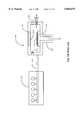
- FIG. 1Bis a cross-section elevation view, mostly diagrammatical, of a conventional CVD processing station as known in the art.
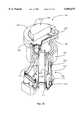
- FIG. 2Ais an isometric view of a multipurpose processing station according to a preferred embodiment of the present invention.
- FIG. 2Bis an exploded view of the multipurpose processing chamber of FIG. 2A.
- FIG. 2Cis an isometric, cutaway elevation view of the multipurpose processing station apparatus of FIG. 2A.
- FIG. 2Dis an elevation section view of the multipurpose processing chamber of FIG. 2A, shown in processing mode.
- FIG. 2Eis an elevation section view of the apparatus of FIG. 2A shown in transfer mode.
- FIG. 3is an elevation section view through a pedestal element, including an electrical feedthrough apparatus, from FIG. 2E.
- FIG. 4Ais an elevation cross-section of the electrical feedthrough apparatus of FIG. 3.
- FIG. 4Bis a section view taken through a body assembly of the feedthrough of FIG. 4A, taken along section line 4B--4B of FIG. 4C.
- FIG. 4Cis a top view of the feedthrough apparatus of FIG. 4A.
- FIG. 5Ais a side elevation view of a ceramic insulator barrier from FIG. 3.
- FIG. 5Bis a plan view of the insulation barrier shown in side view in FIG. 5A.
- FIG. 6Ais an isometric view of a two-zone heater plate in an embodiment of the present invention.
- FIG. 6Bis a plan view of the heater plate of FIG. 6A.
- FIG. 6Cis a side view of the heater plate of FIG. 6A.
- FIG. 7Ais an isometric view a connector post in an embodiment of the present invention.
- FIG. 7Bis an end view of the connector post of FIG. 7A.
- FIG. 7Cis a section view of the connector post of FIG. 7A and FIG. 7B.
- FIG. 1Ais a mostly diagrammatical plan view of a cluster-tool-bases processing system as used both in the prior art and in practicing the present invention.
- the cluster toolitself is a material handling system operating substantially within a vacuum chamber 101.
- a wafer transfer apparatus 103is positioned to operate from the center of the vacuum chamber, and is adapted to place and retrieve, by rotation and extension, substrates, typically semiconductor wafers in IC manufacturing sequences, from and to processing station appended at points around the periphery of substantially circular vacuum transfer chamber 101.
- each of these stationsis adapted to chamber 101 by a mounting flange and slit valve arrangement 102.
- two stations, 5 and 6,are used as airlocks for bringing wafers into and out of chamber 101, which is held under high vacuum by pumping apparatus not shown, and the remaining four stations 1-4 are available for processing.
- Wafersare moved from outside into chamber 101 through load-lock 104, then typically sequentially through the four processing stations, and back to outside through unload lock 105. It is not necessary, however, that the wafers move sequentially through the four processing stations, as transfer apparatus 103 is capable of placing and retrieving in any desired order.
- FIG. 1Bis a cross-section elevation view of station 106 of FIG. 1A, showing some additional typical features of such a processing station.
- Station 106is based on a sealable process chamber interfacing to chamber 101 of FIG. 1A through flanged slit valve apparatus 102. It is through this interface that wafers are brought into chamber 107 for processing, and removed from chamber 107 after processing.
- Chamber 107has a vacuum pumping port 109, through which the chamber is evacuated, and a heatable hearth 110 for supporting a wafer 111 during processing.
- Gases used in processingare introduced from a gas feed and control unit 115 through conduit(s) 114 via ring manifold 113 and showerhead manifold 112.
- chamber 101is pumped by substantial vacuum pumps at all times to keep all of the volume in the chamber under high vacuum.
- the purposeis to avoid contamination by atmospheric gases between processing stations.
- Wafers to be processedare placed in load-lock chamber 104, typically in a carrier, and the load-lock is evacuated to a vacuum level on the order of the vacuum level in chamber 101.
- An inner valveis then opened, and wafers may then be retrieved from the load-lock by transfer apparatus 103 and transferred to any one of processing stations 1-4.
- vacuum pumpingis throttled to control process chamber pressure without using excessive quantities of process gases.
- throttlingmay be accomplished in a number of ways, including valves having controllable openings.
- gasesare valved off in unit 115 (FIG. 1B), and the throttling mechanism is opened to allow maximum pumping speed in the processing chamber.
- the purposeis to reduce the gas pressure in the processing chamber to a value close to that in transfer chamber 107.
- the slit valve in apparatus 102is opened, and transfer apparatus 103 enters the processing chamber and retrieves the processed wafer (111).
- the retrieved waferis typically transferred via apparatus 103 to another processing station, then a wafer from the load-lock or from another processing station is inserted and placed on hearth 111, after which the transfer apparatus withdraws.
- the slit valve associated with apparatus 102is closed again, isolating the process chamber from transfer chamber 101. Then process gases are introduced from unit 115 through conduit(s) 114 and pumping speed is throttled.
- FIG. 2Ais an isometric view of a multipurpose processing station 201 according to a preferred embodiment of the present invention, capable of performing a broad variety of processes
- FIG. 2Bis an exploded view of the multipurpose processing station of FIG. 2A
- FIG. 2Cis an isometric, cutaway elevation view of the multipurpose processing station shown in FIGS. 2A and 2B, seen from a different perspective than that of FIG. 2A
- FIG. 2Dis an elevation section view of the multipurpose processing station of FIG. 2A, shown in processing mode
- FIG. 2Eis an elevation section view of the apparatus of FIG. 2A, shown in transfer mode.
- the multipurpose station in its embodimentsis a relatively complicated apparatus, several views and sections have been provided to better illustrate the features and elements of the station, and the descriptions which follow bearing on the multipurpose processing station are best understood by reference to all of the views provided.
- multipurpose processing station 201is attached to a cluster tool by base chamber 203, which, when assembled with other elements provides vacuum integrity.
- Base chamber 203has a side extending passage 205 ending in a flange 207 which is adapted to mount to a mating flange on a cluster tool transfer apparatus in the manner that station 104 mounts to system 100 (FIG. 1A).
- a slit valveis not shown, and in this embodiment is a part of the cluster tool apparatus to which flange 207 mounts.
- a cylindrical (in this embodiment) processing chamber 204mounts to an upper end of base chamber 203 with vacuum seals providing vacuum integrity at the interface, and a lid assembly 261 seals to the upper end of the process chamber with vacuum seals.
- the lid assembly in this embodimentis hinged to the process chamber and also has apparatus for providing process gases into the process chamber.
- the lid assembly and associated apparatusare described more fully below. For the present portion of the description it is important to note (FIGS. 2C and 2D) that the process chamber with the lid assembly and pedestal provides a closed processing volume.
- a drive assembly 209mounts below to base chamber 203 by a horizontal flange with vacuum seals.
- the horizontal flangeis a part of an upper cylindrical housing 211 which has a side outlet 213 for attachment to a vacuum pumping system not shown.
- Upper housing 211by virtue of being rigidly mounted to base chamber 203, which is in turn rigidly mounted to the vacuum transfer chamber of a cluster tool, is a stationary element providing structural support for other elements, as will be clear from further description below.
- the purpose of the drive assemblyis to raise and lower an internal pedestal apparatus 215 (FIG. 2B).
- the pedestal apparatushas a heated hearth for supporting and providing heat to a wafer to be processed.
- wafersmay be inserted into the base chamber and released to lie upon the hearth, and after the transfer apparatus withdraws through extension 205 and the associated slit valve closes, the pedestal may be raised, moving the supported wafer up into a process chamber in position to be processed.
- Pedestal apparatus 215has an upper portion 217 comprising a heater plate, an electrical insulator plate, and other elements which are described in more detail in sections below.
- the connection of the pedestal apparatus to the drive assemblyis of primary interest.
- FIG. 2Eshows pedestal apparatus 215 in its lowermost position having a wafer 219 supported on upper portion 217 of the pedestal apparatus.
- a transfer apparatus(103 of FIG. 1A) may enter the base chamber through extension 205 and pick and place wafers on the upper portion of the pedestal apparatus.
- wafer 219has been placed on the pedestal apparatus.
- Pedestal apparatus 215has an upper structure 224 and a lower extension 225 ending in a flange 227 to which an outer cylindrical member 223 is also mounted, creating an annular region therebetween.
- Outer cylindrical member 223is lined with a bearing material and is adapted to fit closely around lower housing 221, forming thereby a vertical linear guide for raising and lowering pedestal apparatus 215 reliably with no eccentric loads.
- Vacuum integrityis maintained for the overall assembly while allowing vertical freedom of motion for the pedestal apparatus by a metal bellows 233 which seals between flange 227 at a lower end and a flange 229 affixed by its outer diameter to the lower end of lower cylindrical housing 221.
- Flange 229is stationary, as it is a part of lower housing 221 attached to housing 211 which is mounted to base chamber 203.
- Flange 227by virtue of being attached to lower extension 225 of pedestal apparatus 215, travels up and down with pedestal apparatus 215.
- bellows 233extends, and as pedestal apparatus 215 is raised, bellows 233 retracts.
- the pedestal apparatusis restrained in its vertical path by the inside diameter of flange 229 and primarily by the internal bearing within cylinder 223.
- drive assembly 209includes an electrically actuated and powered linear actuator 235 in this embodiment having an extensible shaft 237 within a guide housing 238, wherein the extensible shaft may be extended and retracted within housing 238 as initiated by control signals received from a control system not shown.
- One end of extensible shaft 237is pivotally attached by a clevis 239 to upper housing 211 of the drive assembly.
- a yoke assembly 241comprising a U-shaped track encircles the body of cylinder 223 (which is fixedly attached to pedestal assembly 215) and is pivotally attached at the ends of the U-shaped track to opposite ends of a clamp bar 243, and the clamp bar clamps on drive housing 238.
- yoke assembly 241engages two bearings 245 which are mounted to opposite sides of cylinder 223.
- one end of an adjustable-length link 247is pivotally fastened by a clevis 249.
- the opposite end of link 247is fastened again to housing 211 by a clevis 251.
- the yoke assemblyis moved as a lever having the attachment at clevis 249 as a fulcrum, such that cylinder 223 is lowered a distance about one-half the length that shaft 237 is extended, causing the entire pedestal assembly be lowered relative to the process chamber and the base chamber.
- the pedestal assemblyis similarly raised relative to the base and process chambers.
- vertical movement of the pedestal assemblywhich provides for a lower position for inserting and retrieving wafers through extension 205, and an upper position wherein a wafer on the pedestal is presented upward into the processing chamber for processing, also provides for a different pumping speed between the upper position and the lower. Also the elements that make this possible also allow for easy alteration of the actual pumping speed in the process position.
- a ring-shaped liner 253is positioned at the point that base chamber 203 joins process chamber 204.
- the inside diameter of liner 253determines area of an annular passage 255 (FIG. 2D) formed between liner 253 and the top edge of pedestal 215 when the pedestal is in the uppermost position.
- Liner 253is also made of a material that has a relatively low coefficient of conductive heat transfer, and thereby provides protection for the parts of the process chamber and the base chamber that are closest to the heated pedestal while the pedestal is in the processing (uppermost) position.
- pedestal 215is provided with an annular shroud 257 which is attached pedestal and forms a shaped pumping annulus.
- a lid assembly 261comprising a lid ring 263, an insulator ring 265 and a gas diff-user assembly 267.
- Gas diffuser assembly 267has ports not shown for introducing process gases, internal passages for conducting the process gases to the process chamber, and diffuser elements within the process region for distributing process gases evenly over a wafer on pedestal 215 in position in the process chamber to be processed. Such ports, passages and distribution elements are well-known in the art.
- Diffuser 267is nested in an insulator ring 265 which provides electrical and thermal insulation for the diffuser assembly, and allows the diffuser assembly to be electrically biased relative to other elements as required in various process recipes. Such bias may be used to, for example, provide for exciting the process gases in the chamber to form a plasma, as known in plasma-enhanced CVD processes.
- Insulator ring 265joins to lid ring 263 and to diffuser 267 in a manner with vacuum seals to provide vacuum integrity and to provide also a rigid lid assembly.
- lid assembly 261is hinged to process chamber 204 with a removable vacuum seal, making access for cleaning and maintenance relatively facile and routine. In other embodiments the lid may be mounted differently and completely removed for access.
- access to the inside of the process chambermay be made by releasing lid assembly 261 and moving it out of the way.
- easy accessis provided to flange 227 where the lower portion 225 is fastened to flange 227.
- With the lid assembly openone may dismount pedestal assembly 215 from flange 227 and remove it from the processing station out the open top.
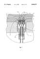
- FIG. 3is a partial cross section through the top region of pedestal 215 at about the position of broken circle 269 in FIG. 2D.
- pedestal 215is an assembly of an upper structure 224 and a lower extension 225.
- Upper structure 224is closed at the top by a closure plate 226, and elements 225, 226, and 224 are assembled with vacuum seals providing an essentially hollow vacuum-tight structure.
- Upper closure plate 226supports heater and electrode elements for supporting a wafer during processing as described more fully below with reference to FIG. 3.
- Closure plate 226 of pedestal assembly 215is the base plate in FIG. 3, and is water-cooled to maintain operating temperature for vacuum seals, such as conventional o-rings and the like, and for other elements that might be damaged by high temperatures.
- closure plate 226is penetrated in this embodiment in two places by a unique electrical feedthrough unit 301.
- a unique electrical feedthrough unit 301is shown in FIG. 3, but in a preferred embodiment there are two such penetrations serving a unique heater plate to be described in detail below.
- Feedthrough unit 301is adapted to closure plate 226 with vacuum seals to preserve vacuum integrity.
- Feedthrough unit 301 in one penetration of closure plate 226provides electrical power to heating elements in a heater plate 303, which is spaced apart from closure plate 226 by in electrical insulator plate 305.
- the function of heater plate 303is to provide heat to a susceptor 307 upon which a wafer rests during processing.
- Susceptor 307is a mostly graphite structure which has a high coefficient of conductive heat transfer, and is spaced apart from heater plate 303 by a small distance D1. Heater plate 303 provides heat to susceptor 307 by convection and radiation across gap D1, helping to provide a relatively constant temperature across its upper surface, hence over the surface of a wafer, and also providing an efficient electrode for high frequency electrical biasing.
- the susceptorforms an electrical entity which, for those processes requiring it, is biased through an RF feedthrough, not shown in FIG. 3.
- Heater power wires connecting to two feedthroughs 301, to a second feedthrough for RF power, and miscellaneous other conduits and connectorsare provided to the region of the lower surface of closure plate 226 by being guided up through the hollow interior of pedestal assembly 215 (See FIGS. 2C, D, and E).
- Such wires and conduits for supplying power and other utilities to pedestal 215 subassemblies and elementsare not shown in these views to promote simplicity, and extend generally from external power and utility supplies as known in the art.
- thermocoupleswith appropriate feedthroughs for sensing temperature of internal elements and at least one optical sensor for monitoring temperature of the susceptor.
- feedthroughsare generally known in the art.
- An air-cylinder -operated mechanism for translating a pattern of typically three ceramic pinsis adapted to the heater/susceptor assembly as well, and is used to raise and lower a wafer from the surface of susceptor 307 to allow a transfer device to extend under a wafer for picking and placing wafers to and from the susceptor plate.
- a pneumatic cylinderis adapted to the underside of closure plate 226 such that the moving shaft of the cylinder may be extended through an opening in the closure plate via a bellows seal.
- the pneumatic cylinderhas a one-half inch stroke and operates a spider positioned below the heater that carries three ceramic pins that extend through small openings in the heater and the susceptor plate.
- a wafer on susceptor 307may be lifted off the upper surface of the susceptor by the ceramic pins referred to above, actuated by the pneumatic cylinder described.
- a transfer arm(see FIG. 1A, item 103) may then extend into the process station beneath the a wafer on the pins but above the susceptor. Retracting the pins then places the wafer on the transfer arm, which may then be withdrawn along with the wafer. The process may be reversed for placing a new wafer to be processed on the susceptor.
- Feedthrough 301 of FIG. 3is shown isolated in FIG. 4A.
- a ceramic body portion 403is joined by intermetallic bonding in this embodiment to a metal body portion 405 which has a seal grove 407 for a vacuum seal such as an o-ring, forming a unitary body sealable through an appropriate opening in closure plate 226 (FIG. 3).
- Solid nickel wires 409are sealed through ceramic body portion 403 also by intermetallic bonding as known in the art, and are joined to conventional power wires 411 such as by soldering, at a distance great enough from the feedthrough that conducted heat will not be a problem.
- sockets 413are constrained in the vertical direction by wires 409, which have considerable stiffness. Openings 415 are somewhat larger in diameter than the diameters of sockets 413, allowing sockets 413 lateral freedom of movement (wires 409 offer little resistance to lateral movement). This freedom of lateral movement allows for some movement and misalignment when assembling a heater plate having posts (as further described below) to a closure plate.
- FIG. 4Cis a top view of feedthrough 301 of FIG. 4A
- FIG. 4Bis a section view taken through the body assembly of feedthrough 301 along section line 4B--4B of FIG. 4C, which is substantially rotated ninety degrees from the section of FIG. 4A
- Section view 4Bis along a groove 417 in ceramic body portion 403 below a circular declavity 419.
- Declavity 419receives a circular portion of heater plate 303 from which connector posts extend, and groove 417 receives a baffle extension 311 of a ceramic insulator barrier 309 which serves to prevent line-of-sight electrical interaction between individual posts of the electrical feedthrough.
- FIG. 5A and Bshow a top view and a side view of ceramic insulator barrier 309, which has an overall diameter great enough to encompass the position of both sockets 413.
- Barrier 309has circular openings 511 and 513 in this embodiment which are adapted to allow posts assembled to heater plate 303 to pass through in a manner that is described in more detail below.
- Baffle extension 311 of barrier 309extends as a barrier wall across the diameter of barrier 309 at substantially ninety degrees to the flat body of the ceramic barrier, and is adapted to engage groove 417 when a heater plate is assembled to a pedestal in the embodiment described.
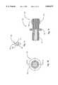
- FIG. 6Ais an isometric view of heater plate 303 of FIG. 3.
- FIG. 6Bis a plan view of the same heater plate
- FIG. 6Cis a side view.
- Heater plate 303 in this embodimentis a unique two-zone heater having an inner region 603 and an outer region 605 separated by a dual channels 607 and 609 which pass through the thickness of the heater plate.
- Inner region 603is adapted to be about the diameter of a wafer to be placed on a susceptor over the heater, and outer region 605 encompasses substantially the remainder of the area of the heater plate.
- Heater plate 303 in this embodimentis a ceramic assembly with thin-film heating elements.
- Two separate connector-post structures 611are constructed on heater plate 303 in this embodiment, one to serve inner region 603 and the other to serve outer region 605.
- the provision of two separate regions capable of being powered independentlyallows tuning heat distribution to combat edge effects in heating a wafer on a susceptor overlying the two-zone heater, which allows a wafer to be heated evenly all the way to the outer diameter, a significant advance over prior art heaters.
- FIGS. 7A, B, and Cillustrate a unique connector post 701 used in the present embodiment in conjunction with the heater plate and socket assembly described above with reference primarily to FIGS. 4A, B, and C.
- FIG. 7Ais an isometric view of connector post 701
- FIG. 7Bis an enlarged end view
- FIG. 7Cis a section view taken along section line 7C--7C of FIG. 7B.
- Connector post 701has a threaded portion 703, a flange 705 and a flexible-finger post extension 707.
- the overall length in the present embodimentis about one-half inch, with about one-quarter inch devoted to each of the threaded portion and the post extension, but larger and smaller posts may be used in other embodiments.
- the thread for the threaded portionis preferably a fine thread, but several different thread sizes may be used.
- connector post extension 707 of connector post 701is divided into 12 equal flexible fingers such as fingers 709 illustrated.
- the connector postis typically made from a chemically-resistant material such as one of several types of stainless steel, and is heat treated in a manner known in the art to provide for appropriate spring tension of the fingers.
- each connector-post structure 611has a raised land 601 with two threaded holes.
- An insulator barrier 309is placed on each raised land, and connector posts 701 are threaded through openings 511 and 513 in the insulator barrier such that flanges 705 capture and hold the insulator barriers against the heater plate.
- Heater plate 303is designed so that the threaded holes allow each heater post to mate with an appropriate heating element in the heater plate. It will be apparent to those with skill in the art that there are many alternative arrangements that might be made in heater design to utilize the unique structure described.
- feedthrough penetrations with feedthroughs 301are provided in closure plate 226 in the pattern required to mate with connector-post structures 611 of a heater plate 303.
- the raised land 601 of each connector-post structureengages circular declavity 419 (see also FIGS. 4A and 4B).
- baffle extension 311 of insulator baffle 309engages groove 417, creating a no-line-of-sight connection.
- sockets 413 on wires 409 of feedthrough 301allow some lateral movement, which, together with the flexible fingers of the posts ensures facile and positive engagement.
- drive assembly 209 described in detail aboveprovides an efficient, smooth and extremely long-life drive for raising and lowering a pedestal assembly in various embodiments of the present invention.
- this driveThere are many variations in this drive that might be used, though, and even completely different drives that might be incorporated in some embodiments while retaining a unique inventive difference over the existing art.
Landscapes
- Chemical & Material Sciences (AREA)
- Engineering & Computer Science (AREA)
- Mechanical Engineering (AREA)
- General Chemical & Material Sciences (AREA)
- Organic Chemistry (AREA)
- Metallurgy (AREA)
- Physics & Mathematics (AREA)
- Materials Engineering (AREA)
- Chemical Kinetics & Catalysis (AREA)
- Power Engineering (AREA)
- Condensed Matter Physics & Semiconductors (AREA)
- General Physics & Mathematics (AREA)
- Microelectronics & Electronic Packaging (AREA)
- Computer Hardware Design (AREA)
- Manufacturing & Machinery (AREA)
- Plasma & Fusion (AREA)
- Analytical Chemistry (AREA)
- Chemical Vapour Deposition (AREA)
- Container, Conveyance, Adherence, Positioning, Of Wafer (AREA)
Abstract
Description
Claims (19)
Priority Applications (8)
| Application Number | Priority Date | Filing Date | Title |
|---|---|---|---|
| US08/810,255US5855675A (en) | 1997-03-03 | 1997-03-03 | Multipurpose processing chamber for chemical vapor deposition processes |
| DE69830310TDE69830310T2 (en) | 1997-03-03 | 1998-03-02 | MULTIFUNCTIONAL PROCESS ROOM FOR CVD PROCESSES |
| EP98908858AEP0972092B1 (en) | 1997-03-03 | 1998-03-02 | Multipurpose processing chamber for chemical vapor deposition processes |
| JP53866898AJP3217798B2 (en) | 1997-03-03 | 1998-03-02 | Versatile process chamber for chemical vapor deposition processes |
| PCT/US1998/004062WO1998039495A1 (en) | 1997-03-03 | 1998-03-02 | Multipurpose processing chamber for chemical vapor deposition processes |
| US09/225,081US6174377B1 (en) | 1997-03-03 | 1999-01-04 | Processing chamber for atomic layer deposition processes |
| US09/764,035US6387185B2 (en) | 1997-03-03 | 2001-01-16 | Processing chamber for atomic layer deposition processes |
| US10/123,293US6818067B2 (en) | 1997-03-03 | 2002-04-15 | Processing chamber for atomic layer deposition processes |
Applications Claiming Priority (1)
| Application Number | Priority Date | Filing Date | Title |
|---|---|---|---|
| US08/810,255US5855675A (en) | 1997-03-03 | 1997-03-03 | Multipurpose processing chamber for chemical vapor deposition processes |
Related Child Applications (3)
| Application Number | Title | Priority Date | Filing Date |
|---|---|---|---|
| US08/920,708Continuation-In-PartUS5879459A (en) | 1997-03-03 | 1997-08-29 | Vertically-stacked process reactor and cluster tool system for atomic layer deposition |
| US09/225,081Continuation-In-PartUS6174377B1 (en) | 1997-03-03 | 1999-01-04 | Processing chamber for atomic layer deposition processes |
| US09/764,035Continuation-In-PartUS6387185B2 (en) | 1997-03-03 | 2001-01-16 | Processing chamber for atomic layer deposition processes |
Publications (1)
| Publication Number | Publication Date |
|---|---|
| US5855675Atrue US5855675A (en) | 1999-01-05 |
Family
ID=25203405
Family Applications (1)
| Application Number | Title | Priority Date | Filing Date |
|---|---|---|---|
| US08/810,255Expired - LifetimeUS5855675A (en) | 1997-03-03 | 1997-03-03 | Multipurpose processing chamber for chemical vapor deposition processes |
Country Status (5)
| Country | Link |
|---|---|
| US (1) | US5855675A (en) |
| EP (1) | EP0972092B1 (en) |
| JP (1) | JP3217798B2 (en) |
| DE (1) | DE69830310T2 (en) |
| WO (1) | WO1998039495A1 (en) |
Cited By (106)
| Publication number | Priority date | Publication date | Assignee | Title |
|---|---|---|---|---|
| WO2000040772A1 (en)* | 1999-01-04 | 2000-07-13 | Genus, Inc. | Processing chamber for atomic layer deposition processes |
| US6144013A (en)* | 1999-07-01 | 2000-11-07 | International Business Machines Corporation | Local humidity control system for low temperature electronic module |
| US6178660B1 (en)* | 1999-08-03 | 2001-01-30 | International Business Machines Corporation | Pass-through semiconductor wafer processing tool and process for gas treating a moving semiconductor wafer |
| US6235656B1 (en) | 2000-07-03 | 2001-05-22 | Andrew Peter Clarke | Dual degas/cool loadlock cluster tool |
| US6364954B2 (en)* | 1998-12-14 | 2002-04-02 | Applied Materials, Inc. | High temperature chemical vapor deposition chamber |
| WO2002033143A1 (en)* | 2000-10-16 | 2002-04-25 | Primaxx, Inc. | Vortex based cvd reactor |
| US20020076508A1 (en)* | 2000-12-15 | 2002-06-20 | Chiang Tony P. | Varying conductance out of a process region to control gas flux in an ALD reactor |
| US20020083897A1 (en)* | 2000-12-29 | 2002-07-04 | Applied Materials, Inc. | Full glass substrate deposition in plasma enhanced chemical vapor deposition |
| US20020108570A1 (en)* | 2000-04-14 | 2002-08-15 | Sven Lindfors | Method and apparatus of growing a thin film onto a substrate |
| US20020114745A1 (en)* | 2001-01-08 | 2002-08-22 | Elliott David J. | Photocatalytic reactor system for treating flue effluents |
| US6472643B1 (en)* | 2000-03-07 | 2002-10-29 | Silicon Valley Group, Inc. | Substrate thermal management system |
| US20020187084A1 (en)* | 1999-07-20 | 2002-12-12 | Sven Lindfors | Method and apparatus for removing substances from gases |
| US6497767B1 (en)* | 1999-05-14 | 2002-12-24 | Tokyo Electron Limited | Thermal processing unit for single substrate |
| US6508197B1 (en) | 1998-09-03 | 2003-01-21 | Cvc Products, Inc. | Apparatus for dispensing gas for fabricating substrates |
| US20030059538A1 (en)* | 2001-09-26 | 2003-03-27 | Applied Materials, Inc. | Integration of barrier layer and seed layer |
| US6547876B2 (en) | 2001-02-07 | 2003-04-15 | Emcore Corporation | Apparatus for growing epitaxial layers on wafers by chemical vapor deposition |
| US6551929B1 (en) | 2000-06-28 | 2003-04-22 | Applied Materials, Inc. | Bifurcated deposition process for depositing refractory metal layers employing atomic layer deposition and chemical vapor deposition techniques |
| US20030079686A1 (en)* | 2001-10-26 | 2003-05-01 | Ling Chen | Gas delivery apparatus and method for atomic layer deposition |
| US6562141B2 (en) | 2000-07-03 | 2003-05-13 | Andrew Peter Clarke | Dual degas/cool loadlock cluster tool |
| US20030121469A1 (en)* | 2000-04-14 | 2003-07-03 | Sven Lindfors | Method and apparatus of growing a thin film |
| US20030127043A1 (en)* | 2001-07-13 | 2003-07-10 | Applied Materials, Inc. | Pulsed nucleation deposition of tungsten layers |
| US20030132213A1 (en)* | 2000-12-29 | 2003-07-17 | Kim Sam H. | Apparatus and method for uniform substrate heating and contaminate collection |
| US20030153181A1 (en)* | 2002-02-11 | 2003-08-14 | Applied Materials, Inc. | Deposition of tungsten films |
| US20030161952A1 (en)* | 2002-02-26 | 2003-08-28 | Applied Materials, Inc. | Cyclical deposition of tungsten nitride for metal oxide gate electrode |
| US6620670B2 (en) | 2002-01-18 | 2003-09-16 | Applied Materials, Inc. | Process conditions and precursors for atomic layer deposition (ALD) of AL2O3 |
| US6620723B1 (en) | 2000-06-27 | 2003-09-16 | Applied Materials, Inc. | Formation of boride barrier layers using chemisorption techniques |
| US20030189232A1 (en)* | 2002-04-09 | 2003-10-09 | Applied Materials, Inc. | Deposition of passivation layers for active matrix liquid crystal display (AMLCD) applications |
| US20030189208A1 (en)* | 2002-04-05 | 2003-10-09 | Kam Law | Deposition of silicon layers for active matrix liquid crystal display (AMLCD) applications |
| US20030190423A1 (en)* | 2002-04-08 | 2003-10-09 | Applied Materials, Inc. | Multiple precursor cyclical deposition system |
| US20030194825A1 (en)* | 2002-04-10 | 2003-10-16 | Kam Law | Deposition of gate metallization for active matrix liquid crystal display (AMLCD) applications |
| US6656330B2 (en)* | 2000-06-22 | 2003-12-02 | Unaxis Balzers Aktiengesellschaft | Coating installation for disk-form workpieces |
| US6660126B2 (en) | 2001-03-02 | 2003-12-09 | Applied Materials, Inc. | Lid assembly for a processing system to facilitate sequential deposition techniques |
| US6692324B2 (en)* | 2000-08-29 | 2004-02-17 | Ut-Battelle, Llc | Single self-aligned carbon containing tips |
| US20040038525A1 (en)* | 2002-08-26 | 2004-02-26 | Shuang Meng | Enhanced atomic layer deposition |
| US6717113B2 (en) | 2000-03-07 | 2004-04-06 | Asml Holding N.V. | Method for substrate thermal management |
| US20040065258A1 (en)* | 2002-10-08 | 2004-04-08 | Sandhu Gurtej S. | Atomic layer deposition methods and atomic layer deposition tools |
| US20040065255A1 (en)* | 2002-10-02 | 2004-04-08 | Applied Materials, Inc. | Cyclical layer deposition system |
| US6720027B2 (en) | 2002-04-08 | 2004-04-13 | Applied Materials, Inc. | Cyclical deposition of a variable content titanium silicon nitride layer |
| US6729824B2 (en) | 2001-12-14 | 2004-05-04 | Applied Materials, Inc. | Dual robot processing system |
| US6734020B2 (en) | 2001-03-07 | 2004-05-11 | Applied Materials, Inc. | Valve control system for atomic layer deposition chamber |
| US20040134427A1 (en)* | 2003-01-09 | 2004-07-15 | Derderian Garo J. | Deposition chamber surface enhancement and resulting deposition chambers |
| US6765178B2 (en) | 2000-12-29 | 2004-07-20 | Applied Materials, Inc. | Chamber for uniform substrate heating |
| US6800173B2 (en) | 2000-12-15 | 2004-10-05 | Novellus Systems, Inc. | Variable gas conductance control for a process chamber |
| US20040209465A1 (en)* | 2000-06-28 | 2004-10-21 | Applied Materials, Inc. | Method and apparatus for depositing refractory metal layers employing sequential deposition techniques to form a nucleation layer |
| US6821563B2 (en) | 2002-10-02 | 2004-11-23 | Applied Materials, Inc. | Gas distribution system for cyclical layer deposition |
| US20050011457A1 (en)* | 2000-12-06 | 2005-01-20 | Chiang Tony P. | Controlling the temperature of a substrate in a film deposition apparatus |
| US20050016471A1 (en)* | 2001-04-05 | 2005-01-27 | Chiang Tony P. | Substrate temperature control in an ALD reactor |
| US6875271B2 (en) | 2002-04-09 | 2005-04-05 | Applied Materials, Inc. | Simultaneous cyclical deposition in different processing regions |
| US6878206B2 (en) | 2001-07-16 | 2005-04-12 | Applied Materials, Inc. | Lid assembly for a processing system to facilitate sequential deposition techniques |
| US20050085102A1 (en)* | 2003-10-16 | 2005-04-21 | Pollock John A. | Coupling and method for producing a hermetic seal |
| US20050136591A1 (en)* | 2001-11-29 | 2005-06-23 | Jae-Hyuck An | Method of and apparatus for performing sequential processes requiring different amounts of time in the manufacturing of semiconductor devices |
| US6911391B2 (en) | 2002-01-26 | 2005-06-28 | Applied Materials, Inc. | Integration of titanium and titanium nitride layers |
| US20050139948A1 (en)* | 2001-09-26 | 2005-06-30 | Applied Materials, Inc. | Integration of barrier layer and seed layer |
| US20050164487A1 (en)* | 2001-02-02 | 2005-07-28 | Applied Materials, Inc. | Formation of a tantalum-nitride layer |
| US20050179097A1 (en)* | 2002-08-22 | 2005-08-18 | Micron Technology, Inc. | Atomic layer deposition of CMOS gates with variable work functions |
| US20050196534A1 (en)* | 2002-11-06 | 2005-09-08 | Tokyo Electron Limited | CVD method using metal carbonyl gas and computer storage medium storing program for controlling same |
| US20060021573A1 (en)* | 2004-06-28 | 2006-02-02 | Cambridge Nanotech Inc. | Vapor deposition systems and methods |
| US6998579B2 (en) | 2000-12-29 | 2006-02-14 | Applied Materials, Inc. | Chamber for uniform substrate heating |
| US6998014B2 (en) | 2002-01-26 | 2006-02-14 | Applied Materials, Inc. | Apparatus and method for plasma assisted deposition |
| US20060060300A1 (en)* | 1997-12-26 | 2006-03-23 | Kazue Takahashi | Plasma treatment method |
| US7049226B2 (en) | 2001-09-26 | 2006-05-23 | Applied Materials, Inc. | Integration of ALD tantalum nitride for copper metallization |
| US7085616B2 (en) | 2001-07-27 | 2006-08-01 | Applied Materials, Inc. | Atomic layer deposition apparatus |
| US20070009658A1 (en)* | 2001-07-13 | 2007-01-11 | Yoo Jong H | Pulse nucleation enhanced nucleation technique for improved step coverage and better gap fill for WCVD process |
| DE102005056323A1 (en)* | 2005-11-25 | 2007-05-31 | Aixtron Ag | Device for simultaneously depositing layers on a number of substrates comprises process chambers arranged in a modular manner in a reactor housing |
| WO2007076195A2 (en) | 2005-11-22 | 2007-07-05 | Genus, Inc. | Small volume symmetric flow single wafer ald apparatus |
| US7262133B2 (en) | 2003-01-07 | 2007-08-28 | Applied Materials, Inc. | Enhancement of copper line reliability using thin ALD tan film to cap the copper line |
| US7270724B2 (en) | 2000-12-13 | 2007-09-18 | Uvtech Systems, Inc. | Scanning plasma reactor |
| US20070240631A1 (en)* | 2006-04-14 | 2007-10-18 | Applied Materials, Inc. | Epitaxial growth of compound nitride semiconductor structures |
| US20070256635A1 (en)* | 2006-05-02 | 2007-11-08 | Applied Materials, Inc. A Delaware Corporation | UV activation of NH3 for III-N deposition |
| KR100797428B1 (en)* | 2000-05-18 | 2008-01-23 | 가부시키가이샤 알박 | Vacuum processing unit and multi-chamber vacuum processing unit |
| US20080131601A1 (en)* | 2003-04-23 | 2008-06-05 | Gi Youl Kim | Transient enhanced atomic layer deposition |
| US7405158B2 (en) | 2000-06-28 | 2008-07-29 | Applied Materials, Inc. | Methods for depositing tungsten layers employing atomic layer deposition techniques |
| US20080206987A1 (en)* | 2007-01-29 | 2008-08-28 | Gelatos Avgerinos V | Process for tungsten nitride deposition by a temperature controlled lid assembly |
| US20090053893A1 (en)* | 2005-01-19 | 2009-02-26 | Amit Khandelwal | Atomic layer deposition of tungsten materials |
| US20090149008A1 (en)* | 2007-10-05 | 2009-06-11 | Applied Materials, Inc. | Method for depositing group iii/v compounds |
| US20090194026A1 (en)* | 2008-01-31 | 2009-08-06 | Burrows Brian H | Processing system for fabricating compound nitride semiconductor devices |
| US7595263B2 (en) | 2003-06-18 | 2009-09-29 | Applied Materials, Inc. | Atomic layer deposition of barrier materials |
| US20090314208A1 (en)* | 2008-06-24 | 2009-12-24 | Applied Materials, Inc. | Pedestal heater for low temperature pecvd application |
| US20100111650A1 (en)* | 2008-01-31 | 2010-05-06 | Applied Materials, Inc. | Automatic substrate loading station |
| US7732327B2 (en) | 2000-06-28 | 2010-06-08 | Applied Materials, Inc. | Vapor deposition of tungsten materials |
| US20100190343A1 (en)* | 2009-01-28 | 2010-07-29 | Asm America, Inc. | Load lock having secondary isolation chamber |
| US20100215854A1 (en)* | 2007-06-24 | 2010-08-26 | Burrows Brian H | Hvpe showerhead design |
| US20100258049A1 (en)* | 2009-04-10 | 2010-10-14 | Applied Materials, Inc. | Hvpe chamber hardware |
| US20100273291A1 (en)* | 2009-04-28 | 2010-10-28 | Applied Materials, Inc. | Decontamination of mocvd chamber using nh3 purge after in-situ cleaning |
| US20100273318A1 (en)* | 2009-04-24 | 2010-10-28 | Applied Materials, Inc. | Substrate pretreatment for subsequent high temperature group iii depositions |
| US20100279020A1 (en)* | 2009-04-29 | 2010-11-04 | Applied Materials, Inc. | METHOD OF FORMING IN-SITU PRE-GaN DEPOSITION LAYER IN HVPE |
| US7867914B2 (en) | 2002-04-16 | 2011-01-11 | Applied Materials, Inc. | System and method for forming an integrated barrier layer |
| US20110070370A1 (en)* | 2008-05-28 | 2011-03-24 | Aixtron Ag | Thermal gradient enhanced chemical vapour deposition (tge-cvd) |
| US20120024479A1 (en)* | 2010-07-30 | 2012-02-02 | Applied Materials, Inc. | Apparatus for controlling the flow of a gas in a process chamber |
| US8183132B2 (en) | 2009-04-10 | 2012-05-22 | Applied Materials, Inc. | Methods for fabricating group III nitride structures with a cluster tool |
| US20120241089A1 (en)* | 2011-03-25 | 2012-09-27 | Applied Materials, Inc. | Method and apparatus for thermocouple installation or replacement in a substrate support |
| US8361892B2 (en) | 2010-04-14 | 2013-01-29 | Applied Materials, Inc. | Multiple precursor showerhead with by-pass ports |
| DE102012103295A1 (en) | 2012-01-09 | 2013-07-11 | Aixtron Se | Device useful for coating semiconductor substrates, comprises processing unit, which is centrally arranged transfer module, loading- or unloading interface, power modules comprising a gas mixing system, pipelines, and a service space |
| US20140072452A1 (en)* | 2012-09-13 | 2014-03-13 | Kla-Tencor Corporation | Apparatus and method for shielding a controlled pressure environment |
| DE102013111790A1 (en) | 2013-10-25 | 2015-04-30 | Aixtron Se | Energy and material consumption optimized CVD reactor |
| DE102013113052A1 (en) | 2013-11-26 | 2015-05-28 | Aixtron Se | Heating device for a CVD reactor |
| US9057128B2 (en) | 2011-03-18 | 2015-06-16 | Applied Materials, Inc. | Multiple level showerhead design |
| US9076827B2 (en) | 2010-09-14 | 2015-07-07 | Applied Materials, Inc. | Transfer chamber metrology for improved device yield |
| US20150293527A1 (en)* | 2014-04-09 | 2015-10-15 | Applied Materials, Inc. | Symmetric chamber body design architecture to address variable process volume with improved flow uniformity/gas conductance |
| US20160020137A1 (en)* | 2014-07-21 | 2016-01-21 | Asm Ip Holding B.V. | Apparatus and method for adjusting a pedestal assembly for a reactor |
| WO2016040547A1 (en)* | 2014-09-11 | 2016-03-17 | Massachusetts Institute Of Technology | Processing system for small substrates |
| US20190032210A1 (en)* | 2017-07-27 | 2019-01-31 | Applied Materials, Inc. | Quick disconnect resistance temperature detector assembly for rotating pedestal |
| US20200291514A1 (en)* | 2019-03-11 | 2020-09-17 | Tokyo Electron Limited | Film Forming Apparatus and Film Forming Method |
| US11066748B2 (en)* | 2014-01-07 | 2021-07-20 | International Business Machines Corporation | Microwave plasma and ultraviolet assisted deposition apparatus and method for material deposition using the same |
| US11270898B2 (en) | 2018-09-16 | 2022-03-08 | Applied Materials, Inc. | Apparatus for enhancing flow uniformity in a process chamber |
| CN115190918A (en)* | 2020-02-14 | 2022-10-14 | 爱思强有限公司 | CVD reactor and method for processing a process chamber cover |
Families Citing this family (4)
| Publication number | Priority date | Publication date | Assignee | Title |
|---|---|---|---|---|
| JP2002343786A (en)* | 2001-05-21 | 2002-11-29 | Tokyo Electron Ltd | Semiconductor treatment equipment |
| JP4820137B2 (en)* | 2005-09-26 | 2011-11-24 | 株式会社日立国際電気 | Heating element holding structure |
| JP5426618B2 (en)* | 2011-07-19 | 2014-02-26 | 株式会社日立国際電気 | Insulating structure, heating apparatus, substrate processing apparatus, and semiconductor device manufacturing method |
| US9412579B2 (en)* | 2012-04-26 | 2016-08-09 | Applied Materials, Inc. | Methods and apparatus for controlling substrate uniformity |
Citations (4)
| Publication number | Priority date | Publication date | Assignee | Title |
|---|---|---|---|---|
| US5078851A (en)* | 1989-07-26 | 1992-01-07 | Kouji Nishihata | Low-temperature plasma processor |
| US5156820A (en)* | 1989-05-15 | 1992-10-20 | Rapro Technology, Inc. | Reaction chamber with controlled radiant energy heating and distributed reactant flow |
| US5294778A (en)* | 1991-09-11 | 1994-03-15 | Lam Research Corporation | CVD platen heater system utilizing concentric electric heating elements |
| US5582866A (en)* | 1993-01-28 | 1996-12-10 | Applied Materials, Inc. | Single substrate vacuum processing apparatus having improved exhaust system |
Family Cites Families (3)
| Publication number | Priority date | Publication date | Assignee | Title |
|---|---|---|---|---|
| JPH06275528A (en)* | 1993-03-18 | 1994-09-30 | Hitachi Ltd | Exhaust part structure of vacuum processor |
| US5772770A (en)* | 1995-01-27 | 1998-06-30 | Kokusai Electric Co, Ltd. | Substrate processing apparatus |
| JPH08260158A (en)* | 1995-01-27 | 1996-10-08 | Kokusai Electric Co Ltd | Substrate processing equipment |
- 1997
- 1997-03-03USUS08/810,255patent/US5855675A/ennot_activeExpired - Lifetime
- 1998
- 1998-03-02WOPCT/US1998/004062patent/WO1998039495A1/enactiveIP Right Grant
- 1998-03-02DEDE69830310Tpatent/DE69830310T2/ennot_activeExpired - Lifetime
- 1998-03-02EPEP98908858Apatent/EP0972092B1/ennot_activeExpired - Lifetime
- 1998-03-02JPJP53866898Apatent/JP3217798B2/ennot_activeExpired - Lifetime
Patent Citations (4)
| Publication number | Priority date | Publication date | Assignee | Title |
|---|---|---|---|---|
| US5156820A (en)* | 1989-05-15 | 1992-10-20 | Rapro Technology, Inc. | Reaction chamber with controlled radiant energy heating and distributed reactant flow |
| US5078851A (en)* | 1989-07-26 | 1992-01-07 | Kouji Nishihata | Low-temperature plasma processor |
| US5294778A (en)* | 1991-09-11 | 1994-03-15 | Lam Research Corporation | CVD platen heater system utilizing concentric electric heating elements |
| US5582866A (en)* | 1993-01-28 | 1996-12-10 | Applied Materials, Inc. | Single substrate vacuum processing apparatus having improved exhaust system |
Cited By (230)
| Publication number | Priority date | Publication date | Assignee | Title |
|---|---|---|---|---|
| US6818067B2 (en)* | 1997-03-03 | 2004-11-16 | Genus, Inc. | Processing chamber for atomic layer deposition processes |
| US6174377B1 (en)* | 1997-03-03 | 2001-01-16 | Genus, Inc. | Processing chamber for atomic layer deposition processes |
| US20020108714A1 (en)* | 1997-03-03 | 2002-08-15 | Kenneth Doering | Processing chamber for atomic layer deposition processes |
| US6387185B2 (en)* | 1997-03-03 | 2002-05-14 | Genus, Inc. | Processing chamber for atomic layer deposition processes |
| US20060060300A1 (en)* | 1997-12-26 | 2006-03-23 | Kazue Takahashi | Plasma treatment method |
| US6692575B1 (en) | 1998-09-03 | 2004-02-17 | Cvc Products Inc. | Apparatus for supporting a substrate in a reaction chamber |
| US6544341B1 (en)* | 1998-09-03 | 2003-04-08 | Cvc Products, Inc. | System for fabricating a device on a substrate with a process gas |
| US6508197B1 (en) | 1998-09-03 | 2003-01-21 | Cvc Products, Inc. | Apparatus for dispensing gas for fabricating substrates |
| US6364954B2 (en)* | 1998-12-14 | 2002-04-02 | Applied Materials, Inc. | High temperature chemical vapor deposition chamber |
| WO2000040772A1 (en)* | 1999-01-04 | 2000-07-13 | Genus, Inc. | Processing chamber for atomic layer deposition processes |
| US6497767B1 (en)* | 1999-05-14 | 2002-12-24 | Tokyo Electron Limited | Thermal processing unit for single substrate |
| US6144013A (en)* | 1999-07-01 | 2000-11-07 | International Business Machines Corporation | Local humidity control system for low temperature electronic module |
| US20020187084A1 (en)* | 1999-07-20 | 2002-12-12 | Sven Lindfors | Method and apparatus for removing substances from gases |
| US7799300B2 (en) | 1999-07-20 | 2010-09-21 | Asm International N.V. | Method and apparatus for removing substances from gases |
| US6178660B1 (en)* | 1999-08-03 | 2001-01-30 | International Business Machines Corporation | Pass-through semiconductor wafer processing tool and process for gas treating a moving semiconductor wafer |
| US6472643B1 (en)* | 2000-03-07 | 2002-10-29 | Silicon Valley Group, Inc. | Substrate thermal management system |
| US6717113B2 (en) | 2000-03-07 | 2004-04-06 | Asml Holding N.V. | Method for substrate thermal management |
| US20030121469A1 (en)* | 2000-04-14 | 2003-07-03 | Sven Lindfors | Method and apparatus of growing a thin film |
| US20020108570A1 (en)* | 2000-04-14 | 2002-08-15 | Sven Lindfors | Method and apparatus of growing a thin film onto a substrate |
| US7060132B2 (en) | 2000-04-14 | 2006-06-13 | Asm International N.V. | Method and apparatus of growing a thin film |
| US7105054B2 (en) | 2000-04-14 | 2006-09-12 | Asm International N.V. | Method and apparatus of growing a thin film onto a substrate |
| KR100797428B1 (en)* | 2000-05-18 | 2008-01-23 | 가부시키가이샤 알박 | Vacuum processing unit and multi-chamber vacuum processing unit |
| US6656330B2 (en)* | 2000-06-22 | 2003-12-02 | Unaxis Balzers Aktiengesellschaft | Coating installation for disk-form workpieces |
| US6620723B1 (en) | 2000-06-27 | 2003-09-16 | Applied Materials, Inc. | Formation of boride barrier layers using chemisorption techniques |
| US7501343B2 (en) | 2000-06-27 | 2009-03-10 | Applied Materials, Inc. | Formation of boride barrier layers using chemisorption techniques |
| US20050118804A1 (en)* | 2000-06-27 | 2005-06-02 | Applied Materials, Inc. | Formation of boride barrier layers using chemisorption techniques |
| US7501344B2 (en) | 2000-06-27 | 2009-03-10 | Applied Materials, Inc. | Formation of boride barrier layers using chemisorption techniques |
| US7208413B2 (en) | 2000-06-27 | 2007-04-24 | Applied Materials, Inc. | Formation of boride barrier layers using chemisorption techniques |
| US7732327B2 (en) | 2000-06-28 | 2010-06-08 | Applied Materials, Inc. | Vapor deposition of tungsten materials |
| US7846840B2 (en) | 2000-06-28 | 2010-12-07 | Applied Materials, Inc. | Method for forming tungsten materials during vapor deposition processes |
| US7115494B2 (en) | 2000-06-28 | 2006-10-03 | Applied Materials, Inc. | Method and system for controlling the presence of fluorine in refractory metal layers |
| US20050059241A1 (en)* | 2000-06-28 | 2005-03-17 | Moris Kori | Method and system for controlling the presence of fluorine in refractory metal layers |
| US7101795B1 (en) | 2000-06-28 | 2006-09-05 | Applied Materials, Inc. | Method and apparatus for depositing refractory metal layers employing sequential deposition techniques to form a nucleation layer |
| US20060128132A1 (en)* | 2000-06-28 | 2006-06-15 | Applied Materials, Inc. | Method and system for controlling the presence of fluorine in refractory metal layers |
| US7745333B2 (en) | 2000-06-28 | 2010-06-29 | Applied Materials, Inc. | Methods for depositing tungsten layers employing atomic layer deposition techniques |
| US6551929B1 (en) | 2000-06-28 | 2003-04-22 | Applied Materials, Inc. | Bifurcated deposition process for depositing refractory metal layers employing atomic layer deposition and chemical vapor deposition techniques |
| US7033922B2 (en) | 2000-06-28 | 2006-04-25 | Applied Materials. Inc. | Method and system for controlling the presence of fluorine in refractory metal layers |
| US20040209465A1 (en)* | 2000-06-28 | 2004-10-21 | Applied Materials, Inc. | Method and apparatus for depositing refractory metal layers employing sequential deposition techniques to form a nucleation layer |
| US7405158B2 (en) | 2000-06-28 | 2008-07-29 | Applied Materials, Inc. | Methods for depositing tungsten layers employing atomic layer deposition techniques |
| US20080280438A1 (en)* | 2000-06-28 | 2008-11-13 | Ken Kaung Lai | Methods for depositing tungsten layers employing atomic layer deposition techniques |
| US7235486B2 (en) | 2000-06-28 | 2007-06-26 | Applied Materials, Inc. | Method for forming tungsten materials during vapor deposition processes |
| US20100093170A1 (en)* | 2000-06-28 | 2010-04-15 | Applied Materials, Inc. | Method for forming tungsten materials during vapor deposition processes |
| US7465666B2 (en) | 2000-06-28 | 2008-12-16 | Applied Materials, Inc. | Method for forming tungsten materials during vapor deposition processes |
| US6855368B1 (en) | 2000-06-28 | 2005-02-15 | Applied Materials, Inc. | Method and system for controlling the presence of fluorine in refractory metal layers |
| US7674715B2 (en) | 2000-06-28 | 2010-03-09 | Applied Materials, Inc. | Method for forming tungsten materials during vapor deposition processes |
| US6235656B1 (en) | 2000-07-03 | 2001-05-22 | Andrew Peter Clarke | Dual degas/cool loadlock cluster tool |
| US6562141B2 (en) | 2000-07-03 | 2003-05-13 | Andrew Peter Clarke | Dual degas/cool loadlock cluster tool |
| US6692324B2 (en)* | 2000-08-29 | 2004-02-17 | Ut-Battelle, Llc | Single self-aligned carbon containing tips |
| WO2002033143A1 (en)* | 2000-10-16 | 2002-04-25 | Primaxx, Inc. | Vortex based cvd reactor |
| US20070184189A1 (en)* | 2000-12-06 | 2007-08-09 | Novellus Systems, Inc. | Controlling the Temperature of a Substrate in a Film Deposition Apparatus |
| US7601393B2 (en) | 2000-12-06 | 2009-10-13 | Novellus Systems, Inc. | Controlling the temperature of a substrate in a film deposition apparatus |
| US20050011457A1 (en)* | 2000-12-06 | 2005-01-20 | Chiang Tony P. | Controlling the temperature of a substrate in a film deposition apparatus |
| US7270724B2 (en) | 2000-12-13 | 2007-09-18 | Uvtech Systems, Inc. | Scanning plasma reactor |
| US6800173B2 (en) | 2000-12-15 | 2004-10-05 | Novellus Systems, Inc. | Variable gas conductance control for a process chamber |
| US20020076508A1 (en)* | 2000-12-15 | 2002-06-20 | Chiang Tony P. | Varying conductance out of a process region to control gas flux in an ALD reactor |
| US7318869B2 (en) | 2000-12-15 | 2008-01-15 | Novellus Systems, Inc. | Variable gas conductance control for a process chamber |
| US20050051100A1 (en)* | 2000-12-15 | 2005-03-10 | Chiang Tony P. | Variable gas conductance control for a process chamber |
| US7189432B2 (en) | 2000-12-15 | 2007-03-13 | Novellus Systems, Inc. | Varying conductance out of a process region to control gas flux in an ALD reactor |
| US7022948B2 (en) | 2000-12-29 | 2006-04-04 | Applied Materials, Inc. | Chamber for uniform substrate heating |
| US20020083897A1 (en)* | 2000-12-29 | 2002-07-04 | Applied Materials, Inc. | Full glass substrate deposition in plasma enhanced chemical vapor deposition |
| US6825447B2 (en) | 2000-12-29 | 2004-11-30 | Applied Materials, Inc. | Apparatus and method for uniform substrate heating and contaminate collection |
| US20050150459A1 (en)* | 2000-12-29 | 2005-07-14 | Quanyuan Shang | Full glass substrate deposition in plasma enhanced chemical vapor deposition |
| US20030132213A1 (en)* | 2000-12-29 | 2003-07-17 | Kim Sam H. | Apparatus and method for uniform substrate heating and contaminate collection |
| US6998579B2 (en) | 2000-12-29 | 2006-02-14 | Applied Materials, Inc. | Chamber for uniform substrate heating |
| US6765178B2 (en) | 2000-12-29 | 2004-07-20 | Applied Materials, Inc. | Chamber for uniform substrate heating |
| US6773683B2 (en) | 2001-01-08 | 2004-08-10 | Uvtech Systems, Inc. | Photocatalytic reactor system for treating flue effluents |
| US20020114745A1 (en)* | 2001-01-08 | 2002-08-22 | Elliott David J. | Photocatalytic reactor system for treating flue effluents |
| US7781326B2 (en) | 2001-02-02 | 2010-08-24 | Applied Materials, Inc. | Formation of a tantalum-nitride layer |
| US8114789B2 (en) | 2001-02-02 | 2012-02-14 | Applied Materials, Inc. | Formation of a tantalum-nitride layer |
| US6951804B2 (en) | 2001-02-02 | 2005-10-04 | Applied Materials, Inc. | Formation of a tantalum-nitride layer |
| US20100311237A1 (en)* | 2001-02-02 | 2010-12-09 | Seutter Sean M | Formation of a tantalum-nitride layer |
| US20060030148A1 (en)* | 2001-02-02 | 2006-02-09 | Applied Materials, Inc. | Formation of a tantalum-nitride layer |
| US7094680B2 (en) | 2001-02-02 | 2006-08-22 | Applied Materials, Inc. | Formation of a tantalum-nitride layer |
| US9012334B2 (en) | 2001-02-02 | 2015-04-21 | Applied Materials, Inc. | Formation of a tantalum-nitride layer |
| US20050164487A1 (en)* | 2001-02-02 | 2005-07-28 | Applied Materials, Inc. | Formation of a tantalum-nitride layer |
| US6547876B2 (en) | 2001-02-07 | 2003-04-15 | Emcore Corporation | Apparatus for growing epitaxial layers on wafers by chemical vapor deposition |
| US6660126B2 (en) | 2001-03-02 | 2003-12-09 | Applied Materials, Inc. | Lid assembly for a processing system to facilitate sequential deposition techniques |
| US9587310B2 (en) | 2001-03-02 | 2017-03-07 | Applied Materials, Inc. | Lid assembly for a processing system to facilitate sequential deposition techniques |
| US7201803B2 (en) | 2001-03-07 | 2007-04-10 | Applied Materials, Inc. | Valve control system for atomic layer deposition chamber |
| US6734020B2 (en) | 2001-03-07 | 2004-05-11 | Applied Materials, Inc. | Valve control system for atomic layer deposition chamber |
| US7806983B2 (en) | 2001-04-05 | 2010-10-05 | Novellus Systems, Inc. | Substrate temperature control in an ALD reactor |
| US20050016471A1 (en)* | 2001-04-05 | 2005-01-27 | Chiang Tony P. | Substrate temperature control in an ALD reactor |
| US6630201B2 (en) | 2001-04-05 | 2003-10-07 | Angstron Systems, Inc. | Adsorption process for atomic layer deposition |
| US7695563B2 (en) | 2001-07-13 | 2010-04-13 | Applied Materials, Inc. | Pulsed deposition process for tungsten nucleation |
| US20070009658A1 (en)* | 2001-07-13 | 2007-01-11 | Yoo Jong H | Pulse nucleation enhanced nucleation technique for improved step coverage and better gap fill for WCVD process |
| US20030127043A1 (en)* | 2001-07-13 | 2003-07-10 | Applied Materials, Inc. | Pulsed nucleation deposition of tungsten layers |
| US20080317954A1 (en)* | 2001-07-13 | 2008-12-25 | Xinliang Lu | Pulsed deposition process for tungsten nucleation |
| US7211144B2 (en) | 2001-07-13 | 2007-05-01 | Applied Materials, Inc. | Pulsed nucleation deposition of tungsten layers |
| US20050115675A1 (en)* | 2001-07-16 | 2005-06-02 | Gwo-Chuan Tzu | Lid assembly for a processing system to facilitate sequential deposition techniques |
| US20110114020A1 (en)* | 2001-07-16 | 2011-05-19 | Gwo-Chuan Tzu | Lid assembly for a processing system to facilitate sequential deposition techniques |
| US6878206B2 (en) | 2001-07-16 | 2005-04-12 | Applied Materials, Inc. | Lid assembly for a processing system to facilitate sequential deposition techniques |
| US10280509B2 (en) | 2001-07-16 | 2019-05-07 | Applied Materials, Inc. | Lid assembly for a processing system to facilitate sequential deposition techniques |
| US7905959B2 (en) | 2001-07-16 | 2011-03-15 | Applied Materials, Inc. | Lid assembly for a processing system to facilitate sequential deposition techniques |
| US7085616B2 (en) | 2001-07-27 | 2006-08-01 | Applied Materials, Inc. | Atomic layer deposition apparatus |
| US7049226B2 (en) | 2001-09-26 | 2006-05-23 | Applied Materials, Inc. | Integration of ALD tantalum nitride for copper metallization |
| US20050139948A1 (en)* | 2001-09-26 | 2005-06-30 | Applied Materials, Inc. | Integration of barrier layer and seed layer |
| US6936906B2 (en) | 2001-09-26 | 2005-08-30 | Applied Materials, Inc. | Integration of barrier layer and seed layer |
| US20060148253A1 (en)* | 2001-09-26 | 2006-07-06 | Applied Materials, Inc. | Integration of ALD tantalum nitride for copper metallization |
| US20070283886A1 (en)* | 2001-09-26 | 2007-12-13 | Hua Chung | Apparatus for integration of barrier layer and seed layer |
| US20030059538A1 (en)* | 2001-09-26 | 2003-03-27 | Applied Materials, Inc. | Integration of barrier layer and seed layer |
| US7494908B2 (en) | 2001-09-26 | 2009-02-24 | Applied Materials, Inc. | Apparatus for integration of barrier layer and seed layer |
| US7352048B2 (en) | 2001-09-26 | 2008-04-01 | Applied Materials, Inc. | Integration of barrier layer and seed layer |
| US6916398B2 (en) | 2001-10-26 | 2005-07-12 | Applied Materials, Inc. | Gas delivery apparatus and method for atomic layer deposition |
| US7780788B2 (en) | 2001-10-26 | 2010-08-24 | Applied Materials, Inc. | Gas delivery apparatus for atomic layer deposition |
| US20100247767A1 (en)* | 2001-10-26 | 2010-09-30 | Ling Chen | Gas delivery apparatus and method for atomic layer deposition |
| US8668776B2 (en) | 2001-10-26 | 2014-03-11 | Applied Materials, Inc. | Gas delivery apparatus and method for atomic layer deposition |
| US20030079686A1 (en)* | 2001-10-26 | 2003-05-01 | Ling Chen | Gas delivery apparatus and method for atomic layer deposition |
| US20050173068A1 (en)* | 2001-10-26 | 2005-08-11 | Ling Chen | Gas delivery apparatus and method for atomic layer deposition |
| US7223702B2 (en) | 2001-11-29 | 2007-05-29 | Samsung Electronics Co., Ltd. | Method of and apparatus for performing sequential processes requiring different amounts of time in the manufacturing of semiconductor devices |
| US20050136591A1 (en)* | 2001-11-29 | 2005-06-23 | Jae-Hyuck An | Method of and apparatus for performing sequential processes requiring different amounts of time in the manufacturing of semiconductor devices |
| US6729824B2 (en) | 2001-12-14 | 2004-05-04 | Applied Materials, Inc. | Dual robot processing system |
| US6620670B2 (en) | 2002-01-18 | 2003-09-16 | Applied Materials, Inc. | Process conditions and precursors for atomic layer deposition (ALD) of AL2O3 |
| US20060075966A1 (en)* | 2002-01-26 | 2006-04-13 | Applied Materials, Inc. | Apparatus and method for plasma assisted deposition |
| US7732325B2 (en) | 2002-01-26 | 2010-06-08 | Applied Materials, Inc. | Plasma-enhanced cyclic layer deposition process for barrier layers |
| US6911391B2 (en) | 2002-01-26 | 2005-06-28 | Applied Materials, Inc. | Integration of titanium and titanium nitride layers |
| US6998014B2 (en) | 2002-01-26 | 2006-02-14 | Applied Materials, Inc. | Apparatus and method for plasma assisted deposition |
| US7473638B2 (en) | 2002-01-26 | 2009-01-06 | Applied Materials, Inc. | Plasma-enhanced cyclic layer deposition process for barrier layers |
| US20060292864A1 (en)* | 2002-01-26 | 2006-12-28 | Yang Michael X | Plasma-enhanced cyclic layer deposition process for barrier layers |
| US7094685B2 (en) | 2002-01-26 | 2006-08-22 | Applied Materials, Inc. | Integration of titanium and titanium nitride layers |
| US7779784B2 (en) | 2002-01-26 | 2010-08-24 | Applied Materials, Inc. | Apparatus and method for plasma assisted deposition |
| US20030153181A1 (en)* | 2002-02-11 | 2003-08-14 | Applied Materials, Inc. | Deposition of tungsten films |
| US6827978B2 (en) | 2002-02-11 | 2004-12-07 | Applied Materials, Inc. | Deposition of tungsten films |
| US6833161B2 (en) | 2002-02-26 | 2004-12-21 | Applied Materials, Inc. | Cyclical deposition of tungsten nitride for metal oxide gate electrode |
| US7115499B2 (en) | 2002-02-26 | 2006-10-03 | Applied Materials, Inc. | Cyclical deposition of tungsten nitride for metal oxide gate electrode |
| US20030161952A1 (en)* | 2002-02-26 | 2003-08-28 | Applied Materials, Inc. | Cyclical deposition of tungsten nitride for metal oxide gate electrode |
| US7745329B2 (en) | 2002-02-26 | 2010-06-29 | Applied Materials, Inc. | Tungsten nitride atomic layer deposition processes |
| US20050176240A1 (en)* | 2002-02-26 | 2005-08-11 | Shulin Wang | Cyclical deposition of tungsten nitride for metal oxide gate electrode |
| US20070020924A1 (en)* | 2002-02-26 | 2007-01-25 | Shulin Wang | Tungsten nitride atomic layer deposition processes |
| US20080305629A1 (en)* | 2002-02-26 | 2008-12-11 | Shulin Wang | Tungsten nitride atomic layer deposition processes |
| US7429516B2 (en) | 2002-02-26 | 2008-09-30 | Applied Materials, Inc. | Tungsten nitride atomic layer deposition processes |
| US7439191B2 (en) | 2002-04-05 | 2008-10-21 | Applied Materials, Inc. | Deposition of silicon layers for active matrix liquid crystal display (AMLCD) applications |
| US20030189208A1 (en)* | 2002-04-05 | 2003-10-09 | Kam Law | Deposition of silicon layers for active matrix liquid crystal display (AMLCD) applications |
| US20030190423A1 (en)* | 2002-04-08 | 2003-10-09 | Applied Materials, Inc. | Multiple precursor cyclical deposition system |
| US6846516B2 (en) | 2002-04-08 | 2005-01-25 | Applied Materials, Inc. | Multiple precursor cyclical deposition system |
| US6720027B2 (en) | 2002-04-08 | 2004-04-13 | Applied Materials, Inc. | Cyclical deposition of a variable content titanium silicon nitride layer |
| US6869838B2 (en) | 2002-04-09 | 2005-03-22 | Applied Materials, Inc. | Deposition of passivation layers for active matrix liquid crystal display (AMLCD) applications |
| US20030189232A1 (en)* | 2002-04-09 | 2003-10-09 | Applied Materials, Inc. | Deposition of passivation layers for active matrix liquid crystal display (AMLCD) applications |
| US6875271B2 (en) | 2002-04-09 | 2005-04-05 | Applied Materials, Inc. | Simultaneous cyclical deposition in different processing regions |
| US20030194825A1 (en)* | 2002-04-10 | 2003-10-16 | Kam Law | Deposition of gate metallization for active matrix liquid crystal display (AMLCD) applications |
| US7867914B2 (en) | 2002-04-16 | 2011-01-11 | Applied Materials, Inc. | System and method for forming an integrated barrier layer |
| US20050179097A1 (en)* | 2002-08-22 | 2005-08-18 | Micron Technology, Inc. | Atomic layer deposition of CMOS gates with variable work functions |
| US7872291B2 (en) | 2002-08-26 | 2011-01-18 | Round Rock Research, Llc | Enhanced atomic layer deposition |
| US8362576B2 (en) | 2002-08-26 | 2013-01-29 | Round Rock Research, Llc | Transistor with reduced depletion field width |
| US6967154B2 (en) | 2002-08-26 | 2005-11-22 | Micron Technology, Inc. | Enhanced atomic layer deposition |
| US20110108929A1 (en)* | 2002-08-26 | 2011-05-12 | Round Rock Research, Llc | Enhanced atomic layer deposition |
| US7279732B2 (en) | 2002-08-26 | 2007-10-09 | Micron Technology, Inc. | Enhanced atomic layer deposition |
| US20040038525A1 (en)* | 2002-08-26 | 2004-02-26 | Shuang Meng | Enhanced atomic layer deposition |
| US8816447B2 (en) | 2002-08-26 | 2014-08-26 | Round Rock Research, Llc | Transistor with reduced depletion field width |
| US20040217410A1 (en)* | 2002-08-26 | 2004-11-04 | Micron Technology, Inc. | Enhanced atomic layer deposition |
| US20080251828A1 (en)* | 2002-08-26 | 2008-10-16 | Micron Technology, Inc. | Enhanced atomic layer deposition |
| US20040065255A1 (en)* | 2002-10-02 | 2004-04-08 | Applied Materials, Inc. | Cyclical layer deposition system |
| US6821563B2 (en) | 2002-10-02 | 2004-11-23 | Applied Materials, Inc. | Gas distribution system for cyclical layer deposition |
| US7279041B2 (en) | 2002-10-08 | 2007-10-09 | Micron Technology, Inc. | Atomic layer deposition methods and atomic layer deposition tools |
| US6916374B2 (en) | 2002-10-08 | 2005-07-12 | Micron Technology, Inc. | Atomic layer deposition methods and atomic layer deposition tools |
| US20050245093A1 (en)* | 2002-10-08 | 2005-11-03 | Sandhu Gurtej S | Atomic layer deposition methods and atomic layer deposition tools |
| US20040065258A1 (en)* | 2002-10-08 | 2004-04-08 | Sandhu Gurtej S. | Atomic layer deposition methods and atomic layer deposition tools |
| US20050196534A1 (en)* | 2002-11-06 | 2005-09-08 | Tokyo Electron Limited | CVD method using metal carbonyl gas and computer storage medium storing program for controlling same |
| US7427426B2 (en)* | 2002-11-06 | 2008-09-23 | Tokyo Electron Limited | CVD method for forming metal film by using metal carbonyl gas |
| US20080311297A1 (en)* | 2002-11-06 | 2008-12-18 | Tokyo Electron Limited | Cvd method using metal carbonyl gas and computer storage medium storing program for controlling same |
| US7879399B2 (en) | 2002-11-06 | 2011-02-01 | Tokyo Electron Limited | CV method using metal carbonyl gas |
| US7262133B2 (en) | 2003-01-07 | 2007-08-28 | Applied Materials, Inc. | Enhancement of copper line reliability using thin ALD tan film to cap the copper line |
| US20040134427A1 (en)* | 2003-01-09 | 2004-07-15 | Derderian Garo J. | Deposition chamber surface enhancement and resulting deposition chambers |
| US20060065635A1 (en)* | 2003-01-09 | 2006-03-30 | Derderian Garo J | Deposition chamber surface enhancement and resulting deposition chambers |
| US20080131601A1 (en)* | 2003-04-23 | 2008-06-05 | Gi Youl Kim | Transient enhanced atomic layer deposition |
| US7981473B2 (en) | 2003-04-23 | 2011-07-19 | Aixtron, Inc. | Transient enhanced atomic layer deposition |
| US7595263B2 (en) | 2003-06-18 | 2009-09-29 | Applied Materials, Inc. | Atomic layer deposition of barrier materials |
| US20050085102A1 (en)* | 2003-10-16 | 2005-04-21 | Pollock John A. | Coupling and method for producing a hermetic seal |
| US6899545B2 (en)* | 2003-10-16 | 2005-05-31 | Special Hermetic Products, Inc. | Coupling and method for producing a hermetic seal |
| US9556519B2 (en) | 2004-06-28 | 2017-01-31 | Ultratech Inc. | Vapor deposition systems and methods |
| US20060021573A1 (en)* | 2004-06-28 | 2006-02-02 | Cambridge Nanotech Inc. | Vapor deposition systems and methods |
| US8202575B2 (en) | 2004-06-28 | 2012-06-19 | Cambridge Nanotech, Inc. | Vapor deposition systems and methods |
| US7964505B2 (en) | 2005-01-19 | 2011-06-21 | Applied Materials, Inc. | Atomic layer deposition of tungsten materials |
| US20090053893A1 (en)* | 2005-01-19 | 2009-02-26 | Amit Khandelwal | Atomic layer deposition of tungsten materials |
| WO2007076195A2 (en) | 2005-11-22 | 2007-07-05 | Genus, Inc. | Small volume symmetric flow single wafer ald apparatus |
| DE102005056323A1 (en)* | 2005-11-25 | 2007-05-31 | Aixtron Ag | Device for simultaneously depositing layers on a number of substrates comprises process chambers arranged in a modular manner in a reactor housing |
| US20070240631A1 (en)* | 2006-04-14 | 2007-10-18 | Applied Materials, Inc. | Epitaxial growth of compound nitride semiconductor structures |
| US20110070721A1 (en)* | 2006-04-14 | 2011-03-24 | Applied Materials, Inc. | Epitaxial growth of compound nitride semiconductor structures |
| US20070256635A1 (en)* | 2006-05-02 | 2007-11-08 | Applied Materials, Inc. A Delaware Corporation | UV activation of NH3 for III-N deposition |
| US20080206987A1 (en)* | 2007-01-29 | 2008-08-28 | Gelatos Avgerinos V | Process for tungsten nitride deposition by a temperature controlled lid assembly |
| US20100215854A1 (en)* | 2007-06-24 | 2010-08-26 | Burrows Brian H | Hvpe showerhead design |
| US20090149008A1 (en)* | 2007-10-05 | 2009-06-11 | Applied Materials, Inc. | Method for depositing group iii/v compounds |
| US20100111650A1 (en)* | 2008-01-31 | 2010-05-06 | Applied Materials, Inc. | Automatic substrate loading station |
| US20090194026A1 (en)* | 2008-01-31 | 2009-08-06 | Burrows Brian H | Processing system for fabricating compound nitride semiconductor devices |
| US20110070370A1 (en)* | 2008-05-28 | 2011-03-24 | Aixtron Ag | Thermal gradient enhanced chemical vapour deposition (tge-cvd) |
| US20090314208A1 (en)* | 2008-06-24 | 2009-12-24 | Applied Materials, Inc. | Pedestal heater for low temperature pecvd application |
| US8927435B2 (en) | 2009-01-28 | 2015-01-06 | Asm America, Inc. | Load lock having secondary isolation chamber |
| US20100190343A1 (en)* | 2009-01-28 | 2010-07-29 | Asm America, Inc. | Load lock having secondary isolation chamber |
| US8440048B2 (en) | 2009-01-28 | 2013-05-14 | Asm America, Inc. | Load lock having secondary isolation chamber |
| US8183132B2 (en) | 2009-04-10 | 2012-05-22 | Applied Materials, Inc. | Methods for fabricating group III nitride structures with a cluster tool |
| US20100258052A1 (en)* | 2009-04-10 | 2010-10-14 | Applied Materials, Inc. | Hvpe precursor source hardware |
| US20100258049A1 (en)* | 2009-04-10 | 2010-10-14 | Applied Materials, Inc. | Hvpe chamber hardware |
| US8491720B2 (en) | 2009-04-10 | 2013-07-23 | Applied Materials, Inc. | HVPE precursor source hardware |
| US8568529B2 (en) | 2009-04-10 | 2013-10-29 | Applied Materials, Inc. | HVPE chamber hardware |
| US8138069B2 (en) | 2009-04-24 | 2012-03-20 | Applied Materials, Inc. | Substrate pretreatment for subsequent high temperature group III depositions |
| US20100273318A1 (en)* | 2009-04-24 | 2010-10-28 | Applied Materials, Inc. | Substrate pretreatment for subsequent high temperature group iii depositions |
| US8110889B2 (en) | 2009-04-28 | 2012-02-07 | Applied Materials, Inc. | MOCVD single chamber split process for LED manufacturing |
| US20100273291A1 (en)* | 2009-04-28 | 2010-10-28 | Applied Materials, Inc. | Decontamination of mocvd chamber using nh3 purge after in-situ cleaning |
| US20100273290A1 (en)* | 2009-04-28 | 2010-10-28 | Applied Materials, Inc. | Mocvd single chamber split process for led manufacturing |
| US20100279020A1 (en)* | 2009-04-29 | 2010-11-04 | Applied Materials, Inc. | METHOD OF FORMING IN-SITU PRE-GaN DEPOSITION LAYER IN HVPE |
| US8361892B2 (en) | 2010-04-14 | 2013-01-29 | Applied Materials, Inc. | Multiple precursor showerhead with by-pass ports |
| US10130958B2 (en) | 2010-04-14 | 2018-11-20 | Applied Materials, Inc. | Showerhead assembly with gas injection distribution devices |
| US9443753B2 (en)* | 2010-07-30 | 2016-09-13 | Applied Materials, Inc. | Apparatus for controlling the flow of a gas in a process chamber |
| US20120024479A1 (en)* | 2010-07-30 | 2012-02-02 | Applied Materials, Inc. | Apparatus for controlling the flow of a gas in a process chamber |
| US9076827B2 (en) | 2010-09-14 | 2015-07-07 | Applied Materials, Inc. | Transfer chamber metrology for improved device yield |
| US10103288B2 (en) | 2010-09-14 | 2018-10-16 | Applied Materials, Inc. | Transfer chamber metrology for improved device yield |
| WO2012069451A2 (en) | 2010-11-25 | 2012-05-31 | Aixtron Se | Thermal gradient enhanced chemical vapour deposition (tge-cvd) |
| US9057128B2 (en) | 2011-03-18 | 2015-06-16 | Applied Materials, Inc. | Multiple level showerhead design |
| US20120241089A1 (en)* | 2011-03-25 | 2012-09-27 | Applied Materials, Inc. | Method and apparatus for thermocouple installation or replacement in a substrate support |
| DE102012103295A1 (en) | 2012-01-09 | 2013-07-11 | Aixtron Se | Device useful for coating semiconductor substrates, comprises processing unit, which is centrally arranged transfer module, loading- or unloading interface, power modules comprising a gas mixing system, pipelines, and a service space |
| US9879684B2 (en)* | 2012-09-13 | 2018-01-30 | Kla-Tencor Corporation | Apparatus and method for shielding a controlled pressure environment |
| TWI614462B (en)* | 2012-09-13 | 2018-02-11 | 克萊譚克公司 | Apparatus and method for shielding a controlled pressure environment |
| US20140072452A1 (en)* | 2012-09-13 | 2014-03-13 | Kla-Tencor Corporation | Apparatus and method for shielding a controlled pressure environment |
| DE102013111790A1 (en) | 2013-10-25 | 2015-04-30 | Aixtron Se | Energy and material consumption optimized CVD reactor |
| DE102013113052A1 (en) | 2013-11-26 | 2015-05-28 | Aixtron Se | Heating device for a CVD reactor |
| US11186911B2 (en) | 2014-01-07 | 2021-11-30 | International Business Machines Corporation | Microwave plasma and ultraviolet assisted deposition apparatus and method for material deposition using the same |
| US11066748B2 (en)* | 2014-01-07 | 2021-07-20 | International Business Machines Corporation | Microwave plasma and ultraviolet assisted deposition apparatus and method for material deposition using the same |
| US10446418B2 (en)* | 2014-04-09 | 2019-10-15 | Applied Materials, Inc. | Symmetric chamber body design architecture to address variable process volume with improved flow uniformity/gas conductance |
| US20150293527A1 (en)* | 2014-04-09 | 2015-10-15 | Applied Materials, Inc. | Symmetric chamber body design architecture to address variable process volume with improved flow uniformity/gas conductance |
| US10727096B2 (en)* | 2014-04-09 | 2020-07-28 | Applied Materials, Inc. | Symmetric chamber body design architecture to address variable process volume with improved flow uniformity/gas conductance |
| US11088015B2 (en) | 2014-07-21 | 2021-08-10 | Asm Ip Holding B.V. | Apparatus for adjusting a pedestal assembly for a reactor |
| US10186450B2 (en)* | 2014-07-21 | 2019-01-22 | Asm Ip Holding B.V. | Apparatus and method for adjusting a pedestal assembly for a reactor |
| US20160020137A1 (en)* | 2014-07-21 | 2016-01-21 | Asm Ip Holding B.V. | Apparatus and method for adjusting a pedestal assembly for a reactor |
| US11417563B2 (en) | 2014-07-21 | 2022-08-16 | Asm America, Inc. | Apparatus and method for adjusting a pedestal assembly for a reactor |
| US10883168B2 (en) | 2014-09-11 | 2021-01-05 | Massachusetts Institute Of Technology | Processing system for small substrates |
| WO2016040547A1 (en)* | 2014-09-11 | 2016-03-17 | Massachusetts Institute Of Technology | Processing system for small substrates |
| US10704142B2 (en)* | 2017-07-27 | 2020-07-07 | Applied Materials, Inc. | Quick disconnect resistance temperature detector assembly for rotating pedestal |
| US20190032210A1 (en)* | 2017-07-27 | 2019-01-31 | Applied Materials, Inc. | Quick disconnect resistance temperature detector assembly for rotating pedestal |
| US11270898B2 (en) | 2018-09-16 | 2022-03-08 | Applied Materials, Inc. | Apparatus for enhancing flow uniformity in a process chamber |
| US20200291514A1 (en)* | 2019-03-11 | 2020-09-17 | Tokyo Electron Limited | Film Forming Apparatus and Film Forming Method |
| CN115190918A (en)* | 2020-02-14 | 2022-10-14 | 爱思强有限公司 | CVD reactor and method for processing a process chamber cover |
Also Published As
| Publication number | Publication date |
|---|---|
| JP2000510652A (en) | 2000-08-15 |
| DE69830310D1 (en) | 2005-06-30 |
| DE69830310T2 (en) | 2006-01-26 |
| EP0972092A1 (en) | 2000-01-19 |
| JP3217798B2 (en) | 2001-10-15 |
| WO1998039495A1 (en) | 1998-09-11 |
| EP0972092A4 (en) | 2002-04-10 |
| EP0972092B1 (en) | 2005-05-25 |
Similar Documents
| Publication | Publication Date | Title |
|---|---|---|
| US5855675A (en) | Multipurpose processing chamber for chemical vapor deposition processes | |
| TWI804537B (en) | Cryogenically cooled rotatable electrostatic chuck | |
| EP1159465B1 (en) | Method of atomic layer deposition | |
| JP3178824B2 (en) | High productivity multi-station type processing equipment for compound single wafer. | |
| US9252037B2 (en) | Vacuum treatment apparatus and a method for manufacturing | |
| US6371712B1 (en) | Support frame for substrates | |
| US20030019428A1 (en) | Chemical vapor deposition chamber | |
| US20090007846A1 (en) | Diffuser gravity support | |
| US11685994B2 (en) | CVD device pumping liner | |
| US20150368830A1 (en) | One-piece injector assembly and one-piece exhaust liner | |
| TWI823158B (en) | Pre-loaded bowl mechanism for providing a symmetric radio frequency return path | |
| US11946140B2 (en) | Hot showerhead | |
| US20240371604A1 (en) | Process module chamber providing symmetric rf return path | |
| KR102864028B1 (en) | Semiconductor processing chamber architecture for higher throughput and faster transfer times | |
| US20250126765A1 (en) | Two-piece rf shield design | |
| US20230095095A1 (en) | Method of isolating the chamber volume to process volume with internal wafer transfer capability | |
| US20240018648A1 (en) | Purge Ring for Reduced Substrate Backside Deposition | |
| KR20230084307A (en) | Dynamic interface to provide a symmetrical radio frequency return path |
Legal Events
| Date | Code | Title | Description |
|---|---|---|---|
| AS | Assignment | Owner name:GENUS, INC., CALIFORNIA Free format text:ASSIGNMENT OF ASSIGNORS INTEREST;ASSIGNORS:DOERING, KENNETH;GALEWSKI, CARL J.;REEL/FRAME:009482/0021 Effective date:19980925 | |
| STCF | Information on status: patent grant | Free format text:PATENTED CASE | |
| AS | Assignment | Owner name:VENTURE BANKING GROUP, CALIFORNIA Free format text:SECURITY INTEREST;ASSIGNOR:GENUS, INC.;REEL/FRAME:010377/0862 Effective date:19991014 | |
| FPAY | Fee payment | Year of fee payment:4 | |
| AS | Assignment | Owner name:SILICON VALLEY BANK, CALIFORNIA Free format text:SECURITY INTEREST;ASSIGNOR:GENUS, INC.;REEL/FRAME:012530/0418 Effective date:20011220 | |
| AS | Assignment | Owner name:GENUS, INC., CALIFORNIA Free format text:RELEASE;ASSIGNOR:SILICON VALLEY BANK;REEL/FRAME:017492/0530 Effective date:20050822 | |
| FPAY | Fee payment | Year of fee payment:8 | |
| FEPP | Fee payment procedure | Free format text:PAT HOLDER NO LONGER CLAIMS SMALL ENTITY STATUS, ENTITY STATUS SET TO UNDISCOUNTED (ORIGINAL EVENT CODE: STOL); ENTITY STATUS OF PATENT OWNER: LARGE ENTITY | |
| FPAY | Fee payment | Year of fee payment:12 | |
| AS | Assignment | Owner name:AIXTRON, INC., CALIFORNIA Free format text:CHANGE OF NAME;ASSIGNOR:GENUS, INC.;REEL/FRAME:042524/0283 Effective date:20060331 |